a new generation of sensors based on extraordinary optical
TRANSCRIPT

A New Generation of Sensors Based onExtraordinary Optical TransmissionREUVEN GORDON,† DAVID SINTON,‡ KAREN L. KAVANAGH,§
AND ALEXANDRE G. BROLO*,⊥†Department of Electrical and Computer Engineering, University of Victoria,
P.O. Box 3055, Victoria, B.C. V8W 3P6, Canada, ‡Department ofMechanical Engineering, University of Victoria, P.O. Box 3055, Victoria,
B.C. V8W 3P6, Canada, §Department of Physics, Simon Fraser University,8888 University Drive, Burnaby, B.C. V5A 1S6, Canada, ⊥ Department of
Chemistry, University of Victoria, P.O. Box 3065, Victoria,B.C. V8W 3V6, Canada
RECEIVED ON MARCH 4, 2008
C O N S P E C T U S
Plasmonic-based chemical sensing technol-ogies play a key role in chemical, biochem-
ical, and biomedical research, but basicresearch in this area is still attracting interest.Researchers would like to develop new typesof plasmonic nanostructures that can improvethe analytical figures of merit, such as detec-tion limits, sensitivity, selectivity, and dynamicrange, relative to the commercial systems.They are also tackling issues such as cost,reproducibility, and multiplexing with the goalof providing the best plasmonic-based plat-form for chemical analysis.
In this Account, we will describe recentadvances in the optical and spectroscopic properties of nanohole arrays in thin gold films and their applications for chem-ical sensing. These nanostructures support the unusual phenomenon of “extraordinary optical transmission” (EOT), that is,they are more transparent at certain wavelengths than expected by the classical aperture theory.
The EOT is a consequence of surface plasmon (SP) excitations; hence, the resonance should respond to the adsorptionof organic molecules. We explored this effect and implemented the integration of the arrays of nanoholes as sensing ele-ments in a microfluidic architecture. We then demonstrated how these devices could be applied in biochemical affinity tests.Arrays of nanoholes offer a small sensing footprint and operate at normal transmission mode, which make them more suit-able for miniaturization. This new approach for SPR sensing is more compatible with the lab-on-chip concept and offersthe possibility of high-throughput analysis from a single sensing chip.
We explored the field localization properties of EOT for surface-enhanced spectroscopy. We could control the enhance-ment factors for SERS and SEFS by adjusting the geometry of the arrays. The shape of the individual nanoholes offers anotherhandle to tune the enhancement factor for surface-enhanced spectroscopy and SPR sensitivity. Apexes in shaped nanostruc-tures function as optical antennas, focusing the light at extremely small regions at the tips. We observed additional sur-face enhancement by tuning the apexes’ properties. The extra enhancement in these cases originated only from the smallnumber of molecules in the apex regions.
The arrays of nanoholes are an exciting new substrate for chemical sensing and enhanced spectroscopy. This class ofnanomaterials has the potential to provide a viable alternative to the commercial SPR-based sensors. Further research couldexploit this platform to develop nanostructures that support high field localization for single-molecule spectroscopy.
Vol. 41, No. 8 August 2008 1049-1057 ACCOUNTS OF CHEMICAL RESEARCH 1049Published on the Web 07/08/2008 www.pubs.acs.org/acr10.1021/ar800074d CCC: $40.75 © 2008 American Chemical Society
1. Introduction
The recent advances in nanofabrication methods1,2 and nano-
particle synthesis3,4 are leading to the advent of a variety of
new nanostructures with unusual physical and chemical prop-
erties. Nanostructured free-electron metals are particularly
interesting, because they can be resonantly excited by visi-
ble light to produce surface plasmon (SP) oscillations.5 SPs are
collective electronic oscillations that lead to surface-bound
electromagnetic fields. They are categorized into two class-
es: propagating surface plasmons or surface plasmons polari-
tons (SPPs)3,5 and localized surface plasmons (LSPs).6 In most
cases, both SPP and LSP resonances are present and contrib-
ute to the optical characteristics of the nanostructure.7 The
manipulation of the properties of SPs by tailoring the geomet-
ric parameters of the nanostructures is the heart of the new
field of plasmonics.5 The plasmonic approach offers an excit-
ing alternative for the manipulation of light in the subwave-
length regime.8 The potential for the development of
plasmonic-based technologies is a major driving force in this
area, and several promising applications have been suggested.
For instance, plasmonic wave-guides could allow the process-
ing of a large amount of information at light speed,3 super-
lensing effects offers a new route to beat diffraction limitations
in imaging systems,9 and the inherent subwavelength con-
finement of the plasmonic field provides a viable alternative
for nanolithography.10 All these examples of application have
the potential to bring revolutionary advancements in informa-
tion processing, device fabrication and imaging technologies.
On the other hand, the plasmonics revolution has already
arrived to the field of chemical sensing, where SP waves are
widely used in important fundamental and practical applica-
tions.2 The capability of SPs to monitor surface-binding events
plays a key role in chemical, biochemical, and biomedical
research.11 The market has responded to the demand for reli-
able plasmonic devices for chemical sensing by providing sev-
eral options for commercial systems that operate based on the
principle of SP excitation.11
There are basically three approaches for SP-based chemi-
cal sensing. The first relies on the dependence of the surface
plasmon resonance (SPR) on the dielectric constant at the
metal-dielectric interface. The SPR is then sensitive to the
changes in refractive indexes provoked by molecular adsorp-
tion, a widely explored property by the bioanalytical commu-
nity to monitor binding events.11 The second approach
explores the red shift in the LSP absorption of metallic nano-
particles (NPs) due to aggregation to devise colorimetric
assays.12 The classical example for the technological applica-
tion of this approach is the Au nanoparticle-based pregnancy
test.13 Finally, the third approach explores the subwavelength
electromagnetic (EM) field localization that accompanies the SP
excitations for enhanced spectroscopy, such as surface-en-
hanced Raman scattering (SERS)14 and surface-enhanced flu-
orescence spectroscopy (SEFS).15 Enhanced spectroscopy
methods allow direct molecular identification and single-mol-
ecule detection limits.14
Plasmonic-based chemical sensing technologies are being
successfully applied and commercialized, and the basic
research in this area is still attracting much interest. The gen-
eral objective is to develop new types of plasmonic nanostruc-
tures that can improve the analytical figures of merit, such as,
detection limits, sensitivity, selectivity, and dynamic range,
provided by the commercial systems. Other issues, such as
cost, reproducibility, and multiplexing, are also tackled, with
the goal of providing the best plasmonic-based platform for
chemical analysis. Following these lines, our group has been
investigating the interesting phenomenon of light transmis-
sion through subwavelength holes (nanoholes) in gold films
and found that this class of substrate may provide a few
advantages over more common chemical sensing platforms.
In this Account, we will discuss our main contributions to this
particular field and propose an outlook for the future direc-
tions of this approach.
2. The Extraordinary Optical Transmission
It is intuitive that the amount of light transmitted through an
aperture in an opaque metal sheet should decrease with the
hole area. The physics behind this phenomenon has been
worked out more than 60 years ago by Bethe,16 who showed
that when the wavelength (λ) of the transmitted light is larger
than the hole diameter (d), the transmittance (T) is given by T
∝ (d/λ)4. A single hole in an infinitely thin slab was consid-
ered in Bethe’s formalism.16 An extension of his approach to
real metals17 and to arrays of holes has been reported.18 The
behavior of nanoholes in real metals with finite thickness was
subsequently explored.19
The idea that the amount of transmitted light decreases
with hole diameter according to Bethe’s law remained unchal-
lenged until 1998, when Ebbesen and co-workers realized a
seminal experiment on the light transmission through arrays
of nanoholes in Ag and Au thin films.20,21 Their result indi-
cated that the amount of transmitted light at certain wave-
lengths was much larger than predicted by the classical
aperture theory. They also demonstrated that there was more
light transmitted than the actual amount that impinged on the
New Generation of Sensors Gordon et al.
1050 ACCOUNTS OF CHEMICAL RESEARCH 1049-1057 August 2008 Vol. 41, No. 8

hole area; that is, the material seemed much more transpar-
ent than it should be. This unexpected phenomenon was
called extraordinary optical transmission (EOT). The effect was
observed for gold and silver films, but its magnitude
decreased when different metals were used. Moreover, the
peaks of maximum transmission were related to the dis-
tance between the nanoholes (periodicity). Considering all
these properties, it was suggested that EOT was due to the
excitation of surface plasmon resonances by a grating cou-
pling.20 Although this interpretation has since been chal-
lenged,22 the evidence from several laboratories seem to
consolidate the excitation of SP as the main contribution to the
EOT effect.23,24
An example of an array of nanoholes on Au that supports
EOT in the visible range is presented in Figure 1A. The array
in Figure 1A was fabricated using focused ion beam (FIB) mill-
ing. The EOT effect is illustrated in Figure 1B where the white
light transmission spectra through arrays of nanoholes of dif-
ferent periodicities are shown. The spectra in Figure 1B were
obtained using a microscope coupled to a miniature spectrom-
eter, as depicted in Figure 1C.25 Peaks in the white light trans-
mission (Figure 1B) correspond to the wavelengths that match
the EOT conditions for each structure. The amount of trans-
mitted light at the peaks far exceeded that expected from the
simple aperture theory.20
For periodic metallic nanostructures, the phase-matching
condition for SPP excitation coincides with the Bragg reso-
nances of the grating. At normal incidence, the wavelength of
SPP resonance (λSP) from an array of nanoholes with square
lattice symmetry can be estimated using20
λSP(i, j) )p� εdεm
εd + εm
√i2 + j2(1)
where p is the lattice constant (periodicity) of the array, i and
j are integers that define the scattering orders of the array, εd
and εm are the real part of the dielectric constants of the adja-
cent medium and the metal, respectively. Equation 1 is for SPs
on a smooth metal-dielectric interface, and it does not
directly apply for meshes. The EOT phenomenon from metal-
lic meshes and its applications have been recently reviewed
elsewhere.27
The zero-order (normal incidence) transmission spectra of
arrays with different periodicities (Figure 1B) shows EOT
slightly red-shifted from that expected from eq 1. Another
interesting feature from the EOT spectra shown in Figure 1B
is the asymmetry around the transmitted peaks. The mini-
mum in the transmission curves, marked with asterisks in Fig-
ure 1B, correspond to a diffraction phenomenon known as
Wood’s anomaly. A Fano analysis has been suggested to
explain the observed red shift of the SP resonance relative to
eq 1 and the line-shape asymmetry in the transmissions.28
The Fano treatment takes into consideration interfering reso-
nant and a nonresonant contributions to the phenomenon. In
the specific case of nanohole arrays, the interference between
the direct transmission through the nanoholes (incoherent
path) and the SP-mediated transmission (coherent path)
accounts for the resonance shift and asymmetry observed
experimentally in EOT.28 On the other hand, recent experi-
ments using two stacked micromeshes, which eliminate the
direct transmission path, still presented asymmetric transmis-
sion peaks.29
EOT was also observed for single holes, and contributions
from LSPs play a key role in these cases.19,30 The light trans-
mission depends strongly on the hole shape. For instance, lon-
gitudinal and transverse LSP modes can be individually
excited in rectangular holes by controlling the electric polar-
ization of the incident light. It has also been found that the cut-
off wavelength for the transmission increases as the width of
the rectangular holes is reduced, which is another counterin-
tuitive result from nanoholes in metals.31 The effect of the
hole shape on the transmission is also observed from arrays
of nanoholes.32,33 Another interesting property related to EOT
from single holes is the “beaming” of the transmitted light,19
which is a preferential direction for the emergent light beam
FIGURE 1. (A) Scanning electron micrograph (SEM) of an array ofnanoholes in a gold film; B) EOT spectra for three arrays withdifferent periodicitiessthe asterisk shows the position of theWood’s anomaly for one of the arrays; (C) experimental setup usedby our group to measure the EOT effect.26 The metal film isdeposited on a glass slide, and the gold side of the array isexposed to solvents and aqueous solutions delivered bymicrofluidics.
New Generation of Sensors Gordon et al.
Vol. 41, No. 8 August 2008 1049-1057 ACCOUNTS OF CHEMICAL RESEARCH 1051

in contrast to the anisotropic distribution expected from sim-
ple diffraction. The beaming phenomenon is more pro-
nounced when a single nanohole is surrounded by a grating
structure.34 In the case of arrays of nanoholes, each hole acts
like a new point source. Therefore, collimated incident light is
recovered as a still collimated output.
3. Exploring EOT for Surface PlasmonResonance SensingThe EOT through arrays of nanoholes depends on the opti-
cal properties of the metal-dielectric interfaces through eq 1.
Therefore, the adsorption of molecules on the gold surface
should shift the transmission peak wavelength, leading to a
SP-mediated chemical sensor. Figure 2 shows a demonstra-
tion of the monolayer sensitivity of the SPR from arrays of
nanoholes reported by our group.25 The white light transmis-
sion spectrum through a clean array of nanoholes (bare Au
surface) presents a distinct resonant peak. The gold surface
was then modified by immersing the array of nanoholes in an
ethanoic solution of mercaptoundecanoic acid (MUA), lead-
ing to a characteristic red shift in the wavelength of maximum
transmission due to the changes in the dielectric properties of
the surface, as predicted by eq 1. Further modification of the
surface by a protein (bovine serum albumin, BSA) provoked an
additional wavelength shift. The spectrum characteristic of a
bare gold surface was recovered after the surface species were
removed by a plasma cleaning treatment.25
The results presented in Figure 2 are reminiscent of the
adsorption-induced shifts in the angle of minimum reflectiv-
ity in typical Kretschmann-configuration surface-plasmon res-
onance (SPR) experiments.11 SPR is one of the most widely
used tools for the study of binding in biochemical systems,
and Figure 2 shows that similar results can be obtained using
arrays of nanoholes.25 In contrast to the commercial SPR sen-
sors, the phase-matching condition for excitation of SPs in
zero-order transmission is given by the periodicity of the holes
(eq 1), and prism coupling is not required. This simplified opti-
cal setup is more suitable for miniaturization.
The combination of all the interesting properties of SP-me-
diated transmission, including the highly localized sensing
area and simple optical setup, render these types of substrates
ideal for the development of integrated biosensors in labora-
tory-on-chip devices. This concept was demonstrated by our
group,26 and the devices investigated are shown in Figure 3A.
Using standard microfluidics fabrication methods, we devel-
oped two configurations of the microfluidic layers, as shown
in Figure 3A. The sensitivity of the integrated arrays of nano-
holes was tested using standard sucrose solutions. The stan-
dard solutions were continuously flowed through the channels
while the whole white light transmission spectra were mea-
sured in real time using the setup shown in Figure 1C. The cal-
ibration curve, presented in Figure 3B, yielded a linear trend
within the range of refractive indexes investigated. The out-
put sensitivity of each array was calculated from the slope of
the calibration curves, averaging ∼333 nm/RIU (RIU ) refrac-
tive index units).26 The sensitivity found in our experiments
agreed well with the values predicted for grating-based SPR
devices35 and are similar to the sensitivities obtained from
sensing schemes based on metallic nanoparticles.36
The devices presented in Figure 3A were also used in affin-
ity tests involving the biotin-streptavidin system.26 Figure 3C
summarized the results of the affinity tests performed using
the arrays of nanoholes as sensor elements in the microflu-
idic device.
The results from Figure 3 demonstrate the potential of
using arrays of nanoholes as sensing elements in laboratory-
on-chip applications. The normal transmission setup allied to
the small footprint of the arrays offers an attractive opportu-
nity for miniaturization. An inexpensive device can be envi-
sioned where the detection of the whole transmission
FIGURE 2. The effects of molecular adsorption on EOT.25
FIGURE 3. (A) Schematic and SEM images illustrating thearchitecture of the microfluidic chips with embedded nanoholearrays; (B) calibration curve using sucrose solutions with differentconcentrations; (C) application of nanoholes for an affinity test.26
New Generation of Sensors Gordon et al.
1052 ACCOUNTS OF CHEMICAL RESEARCH 1049-1057 August 2008 Vol. 41, No. 8

spectrum can be replaced by the measurements of changes in
the amplitude of the transmission from a single laser source,
a concept that has been reported already.37,38
The sensor output sensitivity obtained using the devices
presented in Figure 3A is an order of magnitude smaller than
the values from commercial angle-resolved SPR systems. This
is not a fundamental limitation to the application of arrays of
nanoholes for SPR sensing. It is important to point out that the
sensing area of the arrays of nanoholes is much smaller than
is typical of SPR arrangements; hence, the magnitude of the
wavelength shift from our experiment originates from a
smaller number of molecules. These considerations have been
taken into account by Stark et al.,37 who had demonstrated
better sensitivity and resolution than commercial SPR devices
by measuring the amplitude variations of a laser line through
a short ordered nanohole array. SPR resolution on the order
of commercial devices was also reported by Tetz et al.39 In
that case, they used crossed polarizers to select between the
coherent and the incoherent contributions to the EOT (these
are the contributions that lead to the Fano line shape observed
in Figure 1B). This scheme allows the recovery of a symmet-
rical line shape for the transmission, which provides better
sensitivity.39
4. Nanohole-Enhanced Spectroscopy
The results from Figure 3 show the potential for the applica-
tion of arrays of nanoholes in biomedical sensing and labo-
ratory-on-chip devices. Since the SP fields are tightly confined
to the interface, another powerful approach for chemical sens-
ing is to take advantage of this localization to produce
enhanced molecular spectroscopy. The EM localization is
known as the main contribution to SERS and SEFS.14,15 The
application of SERS and SEFS as a highly sensitive analytical
tool has been described for both random and patterned
substrates.14,40 Nanoholes in noble metals are a promising
platform for enhanced spectroscopy because they not only
confine the EM field but also restrict the analyte to very small
volumes. Moreover, in contrast to colloidal particles dispersed
on glass, the hot spots responsible for the field enhancement
are specifically organized by the nanofabrication of the grat-
ing.41 SERS measurements from a probe molecule, oxazine
720, adsorbed on arrays of nanoholes in gold films were
obtained by our group.42 The experimental geometry (for-
ward scattering) is presented in Figure 4A. The Raman scat-
tering of oxazine 720 was enhanced through the EOT of the
laser excitation. The relationship between the SERS responses
and the periodicity of the arrays was investigated, and it is
shown in Figure 4B.42 The inset in Figure 4B shows the trans-
mission spectra of three arrays with different p-values. The
dashed line corresponds to the laser excitation, fixed at 632.8
nm, and the arrow is to emphasize the position of the SP res-
onance relative to the laser line. It is clear that a strong
enhancement is observed when the laser energy is closer to
the SP excitation (red spectra), and the enhancement
decreases as the separation between the laser energy and the
EOT resonance increases.
The enhancement of the Raman signal was estimated to be
of the order of 105 for oxazine 720 relative to the normal
Raman of liquid benzene. This enhancement factor, however,
includes resonance Raman (RR) contributions, since the laser
excitation at 633 nm is within an electronic absorption of
oxazine 720. Attempts to obtain SERS from other species, such
as rhodamine 6G and pyridine, adsorbed on the nanoholes in
gold were not successful, indicating that the additional RR con-
tribution was essential for the observation of the spectra in Fig-
ure 4B. A quantitative evaluation of the enhancement factor
from nanoholes in silver was realized by Reilly et al.43 An
enhancement factor of 102 due exclusively to the SP excita-
tion through nanoholes was obtained. SERS from randomly
distributed nanoholes in gold films and normal Raman from
single nanoholes in metal were also reported.44,45
Infrared (IR) spectroscopy is another vibrational tool that
provides complementary information to the Raman scatter-
ing. It has been shown that EOT through Ni meshes enhances
the IR absorption from adsorbates.46 A 2 orders of magnitude
enhancement in the IR intensities was observed due to the
increased interaction time provided by the trapped light at the
interface in the form of SP waves.
Although vibrational spectroscopy (Raman and IR) offers
unique spectral characteristics of a chemical species, several
of the current biomedical assays utilize fluorescence probes.
Therefore, there is a great interest in exploring the applicabil-
ity of the arrays of nanoholes as substrates for SEFS,47–51 aim-
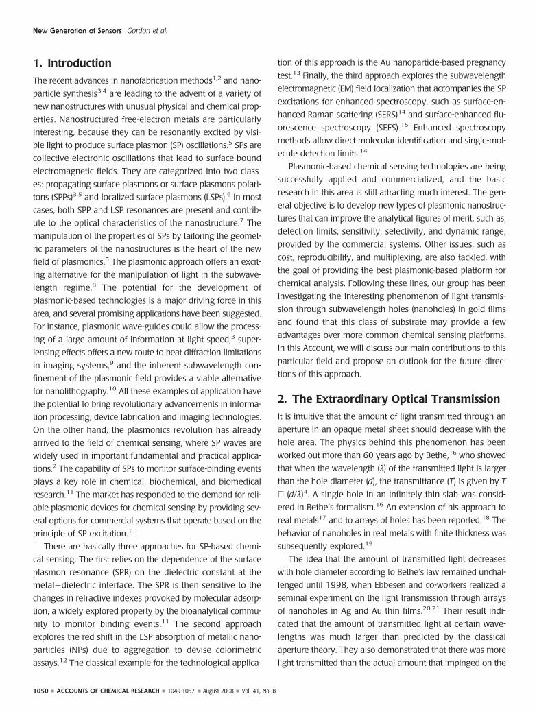
FIGURE 4. (A) Schematic of the forward scattering setup; (B)nanohole-enhanced Raman scattering from oxazine 720 fromnanoholes with different periodicities (p). The inset shows thetransmission spectra of the arrays: (a) p ) 560 nm; (b) p ) 590 nm;(c) p ) 620 nm.42
New Generation of Sensors Gordon et al.
Vol. 41, No. 8 August 2008 1049-1057 ACCOUNTS OF CHEMICAL RESEARCH 1053
ing at further improvement on the sensitivity and limit of
detections of fluorescence-based biomedical tests.
The geometry of our SEFS experiments was similar to the
one presented in Figure 4A, but now the nanoholes were cov-
ered with a polystyrene film doped with the dye.47 The poly-
styrene is necessary because a film thicker than a monolayer
is required for SEFS, due to the well-known fluorescence
quenching experienced by emitters in close proximity to
metallic surfaces. The fluorescence emissions from films of
similar thickness but from arrays of nanoholes with different
periodicities are shown in Figure 5A. The amount of fluores-
cence emissions from the arrays was always larger than
expected from classical aperture theory when the conditions
for SP resonance were achieved.
Another very relevant aspect for chemical analysis that was
noted in our SEFS experiments47 is illustrated in Figure 5B.
The integrated fluorescence from each array was plotted
against the concentration of dye in the film. The slope of these
plots corresponds to the sensitivity from each array. The
results from Figure 5B clearly show that the normalized sen-
sitivity increased by more than three times when the condi-
tions for EOT at the excitation laser frequency were
achieved.47 This is a very important observation because it
demonstrates that not only the detection limit but also the
optical response to concentration changes are optimized by
the plasmonic structure.
5. Enhanced Spectroscopy and Sensingfrom Shaped NanoholesAnother interesting feature that can be explored for chemi-
cal sensing and enhanced spectroscopy is the dependence of
the EOT on the hole shape.7,33,52,53 The anisotropic structures
present selective polarization-dependent transmission. For
instance, we had shown that elliptical holes act as nanopolar-
izers, with preferential transmission when the light field is
polarized perpendicular to the major axis of the ellipse.52 Sim-
ilar effects have been observed for rectangular holes.53 The
line width of the transmission peak was also shown to depend
on the aspect ratio of rectangular apertures;53 therefore, struc-
tures with a sharper transmission band can be devised by geo-
metric optimization to increase sensitivity.
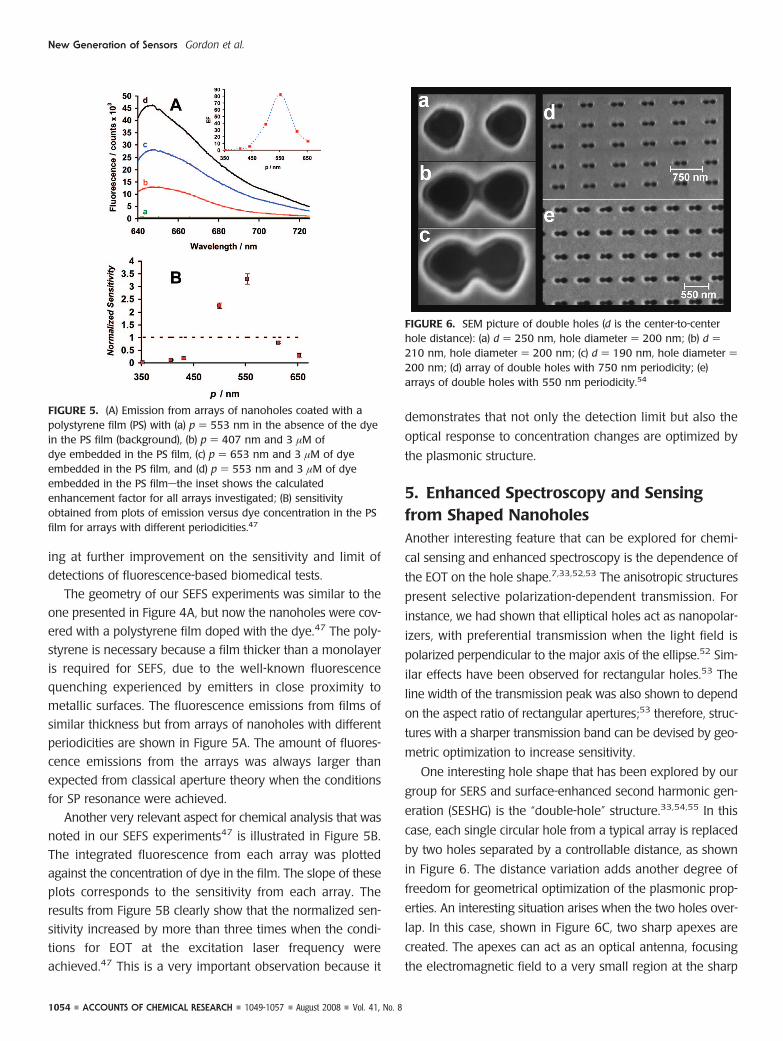
One interesting hole shape that has been explored by our
group for SERS and surface-enhanced second harmonic gen-
eration (SESHG) is the “double-hole” structure.33,54,55 In this
case, each single circular hole from a typical array is replaced
by two holes separated by a controllable distance, as shown
in Figure 6. The distance variation adds another degree of
freedom for geometrical optimization of the plasmonic prop-
erties. An interesting situation arises when the two holes over-
lap. In this case, shown in Figure 6C, two sharp apexes are
created. The apexes can act as an optical antenna, focusing
the electromagnetic field to a very small region at the sharp
FIGURE 5. (A) Emission from arrays of nanoholes coated with apolystyrene film (PS) with (a) p ) 553 nm in the absence of the dyein the PS film (background), (b) p ) 407 nm and 3 µM ofdye embedded in the PS film, (c) p ) 653 nm and 3 µM of dyeembedded in the PS film, and (d) p ) 553 nm and 3 µM of dyeembedded in the PS filmsthe inset shows the calculatedenhancement factor for all arrays investigated; (B) sensitivityobtained from plots of emission versus dye concentration in the PSfilm for arrays with different periodicities.47
FIGURE 6. SEM picture of double holes (d is the center-to-centerhole distance): (a) d ) 250 nm, hole diameter ) 200 nm; (b) d )210 nm, hole diameter ) 200 nm; (c) d ) 190 nm, hole diameter )200 nm; (d) array of double holes with 750 nm periodicity; (e)arrays of double holes with 550 nm periodicity.54
New Generation of Sensors Gordon et al.
1054 ACCOUNTS OF CHEMICAL RESEARCH 1049-1057 August 2008 Vol. 41, No. 8
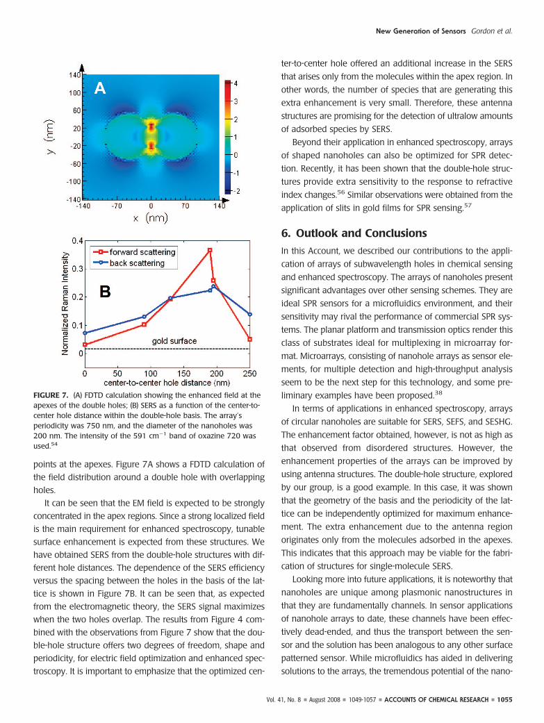
points at the apexes. Figure 7A shows a FDTD calculation of
the field distribution around a double hole with overlapping
holes.
It can be seen that the EM field is expected to be strongly
concentrated in the apex regions. Since a strong localized field
is the main requirement for enhanced spectroscopy, tunable
surface enhancement is expected from these structures. We
have obtained SERS from the double-hole structures with dif-
ferent hole distances. The dependence of the SERS efficiency
versus the spacing between the holes in the basis of the lat-
tice is shown in Figure 7B. It can be seen that, as expected
from the electromagnetic theory, the SERS signal maximizes
when the two holes overlap. The results from Figure 4 com-
bined with the observations from Figure 7 show that the dou-
ble-hole structure offers two degrees of freedom, shape and
periodicity, for electric field optimization and enhanced spec-
troscopy. It is important to emphasize that the optimized cen-
ter-to-center hole offered an additional increase in the SERS
that arises only from the molecules within the apex region. In
other words, the number of species that are generating this
extra enhancement is very small. Therefore, these antenna
structures are promising for the detection of ultralow amounts
of adsorbed species by SERS.
Beyond their application in enhanced spectroscopy, arrays
of shaped nanoholes can also be optimized for SPR detec-
tion. Recently, it has been shown that the double-hole struc-
tures provide extra sensitivity to the response to refractive
index changes.56 Similar observations were obtained from the
application of slits in gold films for SPR sensing.57
6. Outlook and Conclusions
In this Account, we described our contributions to the appli-
cation of arrays of subwavelength holes in chemical sensing
and enhanced spectroscopy. The arrays of nanoholes present
significant advantages over other sensing schemes. They are
ideal SPR sensors for a microfluidics environment, and their
sensitivity may rival the performance of commercial SPR sys-
tems. The planar platform and transmission optics render this
class of substrates ideal for multiplexing in microarray for-
mat. Microarrays, consisting of nanohole arrays as sensor ele-
ments, for multiple detection and high-throughput analysis
seem to be the next step for this technology, and some pre-
liminary examples have been proposed.38
In terms of applications in enhanced spectroscopy, arrays
of circular nanoholes are suitable for SERS, SEFS, and SESHG.
The enhancement factor obtained, however, is not as high as
that observed from disordered structures. However, the
enhancement properties of the arrays can be improved by
using antenna structures. The double-hole structure, explored
by our group, is a good example. In this case, it was shown
that the geometry of the basis and the periodicity of the lat-
tice can be independently optimized for maximum enhance-
ment. The extra enhancement due to the antenna region
originates only from the molecules adsorbed in the apexes.
This indicates that this approach may be viable for the fabri-
cation of structures for single-molecule SERS.
Looking more into future applications, it is noteworthy that
nanoholes are unique among plasmonic nanostructures in
that they are fundamentally channels. In sensor applications
of nanohole arrays to date, these channels have been effec-
tively dead-ended, and thus the transport between the sen-
sor and the solution has been analogous to any other surface
patterned sensor. While microfluidics has aided in delivering
solutions to the arrays, the tremendous potential of the nano-
FIGURE 7. (A) FDTD calculation showing the enhanced field at theapexes of the double holes; (B) SERS as a function of the center-to-center hole distance within the double-hole basis. The array’speriodicity was 750 nm, and the diameter of the nanoholes was200 nm. The intensity of the 591 cm-1 band of oxazine 720 wasused.54
New Generation of Sensors Gordon et al.
Vol. 41, No. 8 August 2008 1049-1057 ACCOUNTS OF CHEMICAL RESEARCH 1055

hole as a conduit has yet to be explored. We feel a flow-
through nanohole array sensing format, as shown in Figure 8,
presents several exciting possibilities: First, analyte transport
via diffusion on the scale of the nanohole is extremely rapid,
and thus flow-through greatly enhances the exposure of the
active area to the solution under test. Likewise, a flow-through
configuration could provide a model platform to study a range
of dynamic processes; analogous electrochemical measure-
ments in nanochannels that harness rapid diffusion on nanos-
cales show much promise.58 Second, flow-through nanohole
arrays, if connected in series with service microfluidics, would
achieve a solution sieving action that is unique among sur-
face-based sensing methods. Just as the nanophotonic struc-
tures enable intense confinement of the electromagnetic field,
flow-through enables sieving and nanoconfinement of an
adsorbed analyte in the same region. Third, while a single
nanohole would present a dominant flow resistance in an oth-
erwise microfluidic system, arrays serve to parallelize the resis-
tance and thus fluid handling and control can be compatible
between the parallel nanochannels and service microfluidics.
Fourthly, flow-through provides access to a previously unex-
ploited portion of the photonic structure and thus potentially
new insight into EOT and new applications. One such appli-
cation would be to immobilize a cell on the surface of a large
array of nanoholes and use access provided by the through-
nanoholes to deliver localized inputs and analyze localized
outputs on the subcellular scale.
One of the glaring limitations to the wide ranging applica-
bility of nanohole arrays in analytical chemistry is the serial
character of the FIB fabrication. However, several methods
for large area patterning have been described in the litera-
ture.24,59 These new lithographic methods offer a promising
avenue to overcome this limitation.
We gratefully acknowledge funding support for this work from
NSERC, CFI, and BCKDF. We also thank current support through
a NSERC SPG with the BC Cancer Agency and Micralyne Inc.
BIOGRAPHICAL INFORMATION
Reuven Gordon is an Associate Professor in Electrical and Com-puter Engineering at the University of Victoria. His recent researchcontributions have been mainly in the area of nanophotonics.
David Sinton is an Assistant Professor in Mechanical Engineer-ing at the University of Victoria. His research area is in micro- andnanofluidics.
Karen L. Kavanagh is a Physics Professor at Simon Fraser Uni-versity. Her main fields of interest are electronic materials sci-ence and nanofabrication.
Alexandre G. Brolo is an Associate Professor of Chemistry at theUniversity of Victoria. His current interests are on the develop-ment of substrates for enhanced spectroscopy and chemicalsensing.
FOOTNOTES
*To whom correspondence should be addressed. Phone: 1 250 721 7167. Fax: 1 250 7217147. E-mail: [email protected].
REFERENCES1 Gates, B. D.; Xu, Q. B.; Stewart, M.; Ryan, D.; Willson, C. G.; Whitesides, G. M. New
approaches to nanofabrication: Molding, printing, and other techniques. Chem. Rev.2005, 105, 1171–1196.
2 Willets, K. A.; Van Duyne, R. P. Localized surface plasmon resonance spectroscopyand sensing. Annu. Rev. Phys. Chem. 2007, 58, 267–297.
3 Lal, S.; Link, S.; Halas, N. J. Nano-optics from sensing to waveguiding. Nat.Photonics 2007, 1, 641–648.
4 Zhang, J. H.; Liu, H. Y.; Wang, Z. L.; Ming, N. B. Shape-selective synthesis of goldnanoparticles with controlled sizes, shapes, and plasmon resonances. Adv. Funct.Mater. 2007, 17, 3295–3303.
5 Barnes, W. L.; Dereux, A.; Ebbesen, T. W. Surface plasmon subwavelength optics.Nature 2003, 424, 824–830.
6 Zhao, J.; Zhang, X. Y.; Yonzon, C. R.; Haes, A. J.; Van Duyne, R. P. Localizedsurface plasmon resonance biosensors. Nanomedicine 2006, 1, 219–228.
7 Degiron, A.; Ebbesen, T. W. The role of localized surface plasmon modes in theenhanced transmission of periodic subwavelength apertures. J. Opt. A: Pure Appl.Opt. 2005, 7, S90-S96.
8 Ozbay, E. Plasmonics: Merging photonics and electronics at nanoscale dimensions.Science 2006, 311, 189–193.
9 Fang, N.; Lee, H.; Sun, C.; Zhang, X. Sub-diffraction-limited optical imaging with asilver superlens. Science 2005, 308, 534–537.
10 Wei, X. Z.; Luo, X. G.; Dong, X. C.; Du, C. L. Localized surface plasmonnanolithography with ultrahigh resolution. Opt. Express 2007, 15, 14177–14183.
11 Homola, J. Surface plasmon resonance sensor for detection of chemical andbiological species. Chem. Rev. 2008, 108, 462–493.
12 Rosi, N. L.; Mirkin, C. A. Nanostructures in biodiagnostics. Chem. Rev. 2005, 105,1547–1562.
13 Bangs, L. B. New developments in particle-based immunoassays: Introduction. PureAppl. Chem. 1996, 68, 1873–1879.
14 Aroca, R. Surface-Enhanced Vibrational Spectroscopy; Wiley: Chichester, U.K.;Hoboken, NJ, 2006.
FIGURE 8. Schematic of flow-through nanohole array sensing asintegrated in a chip-and-reader configuration. Flow to and throughthe nanohole/nanofluidic layer is facilitated by microfluidic servicelayers on top and bottom.
New Generation of Sensors Gordon et al.
1056 ACCOUNTS OF CHEMICAL RESEARCH 1049-1057 August 2008 Vol. 41, No. 8

15 Lakowicz, J. R. Plasmonics in biology and plasmon-controlled fluorescence.Plasmonics 2006, 1, 5–33.
16 Bethe, H. A. Theory of diffraction by small holes. Phys. Rev. 1944, 66, 163–182.17 Wannemacher, R. Plasmon-supported transmission of light through nanometric
holes in metallic thin films. Opt. Commun. 2001, 195, 107–118.18 Gordon, R. Bethe’s aperture theory for arrays. Phys. Rev. A 2007, 76, 053806.19 Degiron, A.; Lezec, H. J.; Yamamoto, N.; Ebbesen, T. W. Optical transmission
properties of a single subwavelength aperture in a real metal. Opt. Commun. 2004,239, 61–66.
20 Ebbesen, T. W.; Lezec, H. J.; Ghaemi, H. F.; Thio, T.; Wolff, P. A. Extraordinaryoptical transmission through sub wavelength hole arrays. Nature 1998, 391, 667–669.
21 Genet, C.; Ebbesen, T. W. Light in tiny holes. Nature 2007, 445, 39–46.22 Lezec, H. J.; Thio, T. Diffracted evanescent wave model for enhanced and
suppressed optical transmission through subwavelength hole arrays. Opt. Express2004, 12, 3629–3651.
23 Huang, C. P.; Wang, Q. J.; Zhu, Y. Y. Dual effect of surface plasmons in lighttransmission through perforated metal films. Phys. Rev. B 2007, 75, 245921.
24 Gao, H. W.; Henzie, J.; Odom, T. W. Direct evidence for surface plasmon-mediatedenhanced light transmission through metallic nanohole arrays. Nano Lett. 2006, 6,2104–2108.
25 Brolo, A. G.; Gordon, R.; Leathem, B.; Kavanagh, K. L. Surface plasmon sensorbased on the enhanced light transmission through arrays of nanoholes in gold films.Langmuir 2004, 20, 4813–4815.
26 De Leebeeck, A.; Kumar, L. K. S.; de Lange, V.; Sinton, D.; Gordon, R.; Brolo, A. G.On-chip surface-based detection with nanohole arrays. Anal. Chem. 2007, 79,4094–4100.
27 Coe, J. V.; Heer, J. M.; Teeters-Kennedy, S.; Tian, H.; Rodriguez, K. R. Extraordinarytransmission of metal films with arrays of subwavelength holes. Annu. Rev. Phys.Chem. 2008, 59, 179–202.
28 Genet, C.; van Exter, M. P.; Woerdman, J. P. Fano-type interpretation of red shiftsand red tails in hole array transmission spectra. Opt. Commun. 2003, 225, 331–336.
29 Teeters-Kennedy, S.; Williams, S. M.; Rodriguez, K. R.; Cilwa, K.; Meleason, D.;Sudnitsyn, A.; Hrovat, F.; Coe, J. V. Extraordinary infrared transmission of a stack oftwo metal micromeshes. J. Phys. Chem. C 2007, 111, 124–130.
30 Rindzevicius, T.; Alaverdyan, Y.; Sepulveda, B.; Pakizeh, T.; Kall, M.; Hillenbrand, R.;Aizpurua, J.; de Abajo, F. J. G. Nanohole plasmons in optically thin gold films. J.Phys. Chem. C 2007, 111, 1207–1212.
31 Gordon, R.; Brolo, A. G. Increased cut-off wavelength for a subwavelength hole in areal metal. Opt. Express 2005, 13, 1933–1938.
32 van der Molen, K. L.; Klein Koerkamp, K. J.; Enoch, S.; Segerink, F. B.; van Hulst,N. F.; Kuipers, L. Role of shape and localized resonances in extraordinarytransmission through periodic arrays of subwavelength holes: Experiment andtheory. Phys. Rev. B 2005, 72, 045421.
33 Gordon, R.; Hughes, M.; Leathem, B.; Kavanagh, K. L.; Brolo, A. G. Basis and latticepolarization mechanisms for light transmission through nanohole arrays in a metalfilm. Nano Lett. 2005, 5, 1243–1246.
34 Lezec, H. J.; Degiron, A.; Devaux, E.; Linke, R. A.; Martin-Moreno, L.; Garcia-Vidal,F. J.; Ebbesen, T. W. Beaming light from a subwavelength aperture. Science 2002,297, 820–822.
35 Moharam, M. G.; Gaylord, T. K. Rigorous Coupled-Wave Analysis of MetallicSurface-Relief Gratings. J. Opt. Soc. Am. A 1986, 3, 1780–1787.
36 Sun, Y. G.; Xia, Y. N. Gold and silver nanoparticles: A class of chromophores withcolors tunable in the range from 400 to 750 nm. Analyst 2003, 128, 686–691.
37 Stark, P. R. H.; Halleck, A. E.; Larson, D. N. Short order nanohole arrays in metalsfor highly sensitive probing of local indices of refraction as the basis for a highlymultiplexed biosensor technology. Methods 2005, 37, 37–47.
38 Lesuffleur, A.; Im, H.; Lindquist, N. C.; Lim, K. S.; Oh, S. H. Laser-illuminatednanohole arrays for multiplex plasmonic microarray sensing. Opt. Express 2008, 16,219–224.
39 Tetz, K. A.; Pang, L.; Fainman, Y. High-resolution surface plasmon resonancesensor based on linewidth-optimized nanohole array transmittance. Opt. Lett. 2006,31, 1528–1530.
40 Andrew, P.; Barnes, W. L. Molecular fluorescence above metallic gratings. Phys.Rev. B 2001, 64, 125405.
41 Krishnan, A.; Thio, T.; Kim, T. J.; Lezec, H. J.; Ebbesen, T. W.; Wolff, P. A.; Pendry,J.; Martin-Moreno, L.; Garcia-Vidal, F. J. Evanescently coupled resonances in SPenhanced transmission. Opt. Commun. 2001, 200, 1–7.
42 Brolo, A. G.; Arctander, E.; Gordon, R.; Leathem, B.; Kavanagh, K. L. Nanohole-enhanced Raman scattering. Nano Lett. 2004, 4, 2015–2018.
43 Reilly, T. H.; Chang, S. H.; Corbman, J. D.; Schatz, G. C.; Rowlen, K. L. Quantitativeevaluation of plasmon enhanced Raman scattering from nanoaperture arrays. J.Phys. Chem. C 2007, 111, 1689–1694.
44 Bahns, J. T.; Yan, F. N.; Qiu, D. L.; Wang, R.; Chen, L. H. Hole-enhanced Ramanscattering. Appl. Spectrosc. 2006, 60, 989–993.
45 Wenger, J.; Dintinger, J.; Bonod, N.; Popov, E.; Lenne, P. F.; Ebbesen, T. W.;Rigneault, H. Raman scattering and fluorescence emission in a singlenanoaperture: Optimizing the local intensity enhancement. Opt. Commun. 2006,267, 224–228.
46 Coe, J. V.; Rodriguez, K. R.; Teeters-Kennedy, S.; Cilwa, K.; Heer, J.; Tian, H.;Williams, S. M. Metal films with Arrays of tiny holes: Spectroscopy with infraredplasmonic scaffolding. J. Phys. Chem. C 2007, 111, 17459–17472.
47 Brolo, A. G.; Kwok, S. C.; Moffitt, M. G.; Gordon, R.; Riordon, J.; Kavanagh, K. L.Enhanced fluorescence from arrays of nanoholes in a gold film. J. Am. Chem. Soc.2005, 127, 14936–14941.
48 Stark, P. R. H.; Halleck, A. E.; Larson, D. N. Breaking the diffraction barrier outsideof the optical near-field with bright, collimated light from nanometric apertures.Proc. Natl. Acad. Sci. U.S.A. 2007, 104, 18902–18906.
49 Brolo, A. G.; Kwok, S. C.; Cooper, M. D.; Moffitt, M. G.; Wang, C. W.; Gordon, R.;Riordon, J.; Kavanagh, K. L. Surface plasmon-quantum dot coupling from arrays ofnanoholes. J. Phys. Chem. B 2006, 110, 8307–8313.
50 Liu, Y.; Bishop, J.; Williams, L.; Blair, S.; Herron, J. Biosensing based uponmolecular confinement in metallic nanocavity arrays. Nanotechnology 2004, 15,1368–1374.
51 Blair, S.; Chen, Y. Resonant-enhanced evanescent-wave fluorescence biosensingwith cylindrical optical cavities. Appl. Opt. 2001, 40, 570–582.
52 Gordon, R.; Brolo, A. G.; McKinnon, A.; Rajora, A.; Leathem, B.; Kavanagh, K. L.Strong polarization in the optical transmission through ellipticall nanohole arrays.Phys. Rev. Lett. 2004, 92, 037401.
53 Koerkamp, K. J. K.; Enoch, S.; Segerink, F. B.; Hulst, N. F. v.; Kuipers, L. StrongInfluence of hole shape on extraordinary transmission through periodic arrays ofnanoholes. Phys. Rev. Lett. 2004, 92, 183901.
54 Lesuffleur, A.; Kumar, L. K. S.; Brolo, A. G.; Kavanagh, K. L.; Gordon, R. Apex-enhanced Raman spectroscopy using double-hole arrays in a gold film. J. Phys.Chem. C 2007, 111, 2347–2350.
55 Lesuffleur, A.; Kumar, L. K. S.; Gordon, R. Apex-enhanced second-harmonicgeneration by using double-hole arrays in a gold film. Phys. Rev. B 2007, 75,045423.
56 Lesuffleur, A.; Im, H.; Lindquist, N. C.; Oh, S. H. Periodic nanohole arrays withshape-enhanced plasmon resonance as real-time biosensors. Appl. Phys. Lett.2007, 90, 261104.
57 Lee, K. L.; Lee, C. W.; Wang, W. S.; Wei, P. K. Sensitive biosensor array usingsurface plasmon resonance on metallic nanoslits. J. Biomed. Opt. 2007, 12,044023.
58 Zevenbergen, M. A. G.; Krapf, D.; Zuiddam, M. R.; Lemay, S. G. Mesoscopicconcentration fluctuations in a fluidic nanocavity detected by redox cycling. NanoLett. 2007, 7, 384–388.
59 Lim, C. S.; Hong, M. H.; Lin, Y.; Xie, Q.; Luk’yanchuk, B. S.; Kumar, A. S.; Rahman,M. Microlens array fabrication by laser interference lithography for super-resolutionsurface nanopatterning. Appl. Phys. Lett. 2006, 89, 191125.
New Generation of Sensors Gordon et al.
Vol. 41, No. 8 August 2008 1049-1057 ACCOUNTS OF CHEMICAL RESEARCH 1057