a multiport medium voltage isolated dc-dc converter · the multiport converter is suited for...
TRANSCRIPT

A Multiport Medium Voltage Isolated DC-DCConverter
Yan-Kim Tran, Drazen DujicEcole Polytechnique Federale de Lausanne - EPFL
Power Electronics Laboratory - PEL
Station 11, CH-1015, Lausanne
[email protected], [email protected]
Abstract—A multiport medium voltage (MV) isolated DC-DCconverter with integrated energy storage, suited for connection oflow voltage (LV) and medium voltage (MV) DC grids is presented.A multi-stage structure, adapted for MV ratings, is composedof multiple identical submodules connected in an Input-Series-Output-Parallel (ISOP) configuration. Each submodule has threefully bidirectional ports, that are galvanically isolated. Thisis achieved by means of a three-winding medium frequencytransformer, where each leakage inductance combined with aresonant capacitor creates a resonant tank, benefiting fromsoft switching operation. Each submodule has two additionalbuck/boost stages, to actively control the power exchange withexternal DC circuits. The inner resonant stage is operated inopen-loop and adapts its mode of operation based on the actualpower flow. The remaining ports, dedicated to the storage, canbe operated independently from the power flow between the MVand LV side, in order to charge or discharge the storage elements.Switched mode simulations are used to verify and demonstratevarious operational modes and performance of the converter.
Index Terms—MVDC, Multiport, DC-DC, Resonant Converter
I. INTRODUCTION
The weakness of the renewable energy sources is their
climate dependency and consequent volatility, which can be
partly compensated by a judicious geographic distribution and
further supported through the integration of storage technolo-
gies. This implies a need for new types of grids, able to
support more interconnections, integrate energy buffers while
providing flexible and reliable operation. To avoid unnecessary
power circulation and save some capacity in the transport
infrastructures, the energy should be stored close to its pro-
duction in order to be consumed by the surrounding loads.
This would limit the grid solicitation only to temporary flow
of the surplus or lack of power. The MVDC grids are seen
as feasible solution to the link between low/medium voltage
generation/distribution and existing high voltage transmission
lines [1]. They can reinforce existing and future power dis-
tribution networks efficiently, considering that renewable and
energy storage technologies are inherently DC and low-voltage
by nature, respectively [2].
To enhance reliability, flexibility and efficiency of the
charge-discharge cycle of the storage elements, the multiport
DC-DC converters offer interesting prospects [3]. Although the
converters based on the connection of multiple ports through
a non-isolated common DC bus offer a certain simplicity of
control, they have a limited range of voltage conversion ratio.
The literature presents some galvanically isolated topologies
based on multi-winding transformers derived from the Dual-
Active-Bridge (DAB) and extended with a third winding [4]
and [5] or even two additional ports [6]. While they have the
advantages of the freedom to set the turn ratio accordingly,
allowing grids of different voltages to be interfaced, their
power flow control is done through phase-shift or PWM that
results in a reduced soft switching operation range. A multiport
resonant converter, having Medium Frequency Transformers
(MFTs) combined with distributed resonant capacitors, is
presented in [7], with one source port and two load ports
operated in open loop. Similarly, [8] presents topology with
two sources and one load where the power flow and the load
sharing are regulated through a phase-shift control. While
these two LLC resonant converters demonstrate some benefits
in terms of soft switching, they are suitable only for low
voltage and low power applications.
The MV insulation constraints can be overcome by the use
of some multi-stacked-stage structures, reducing the voltage
stresses on the semiconductor devices. Such a solution has
many advantages as highlighted in [9]. The overall system
availability/reliability is increased, due to redundancy of the
key elements and due to the distribution of the electrical
and thermal stresses between the stages. In the case of a
large voltage conversion ratios, the ISOP structure has some
advantages due to the split of the voltage on the series side
(high-voltage/low-current) and the current sharing on the par-
allel side (low-voltage/high-current). The ISOP structure has
been demonstrated for a power electronic traction transformer
where multiple LLC resonant circuits are used in a multi-
stage configuration [10] while the IPOS resonant topology is
presented in [11].
The topology of a novel medium voltage multiport converter
is proposed in this paper. It is the ISOP combination of
multiple submodules based on the structure presented in [12].
The multiport converter is suited for bidirectional interfacing
of MVDC and LVDC grids, through the two main ports, while
the third port of each submodule is dedicated to the connection
of low voltage storage elements with reduced ratings (e.g. 0.2
p.u.). Each submodule is composed by a three winding MFT
and additional capacitors creating a distributed LLC resonant
tank. The resonant components are tuned on the three sides
L1
L2
L3
S2
S3 S5
S4
Lm
LB4
S1
MFT+ResonantTank
VDC1
V1
CDC1
CDC2
CDC3 VDC3
VDC2
V3
Cr1
Cr2
Cr3LB5
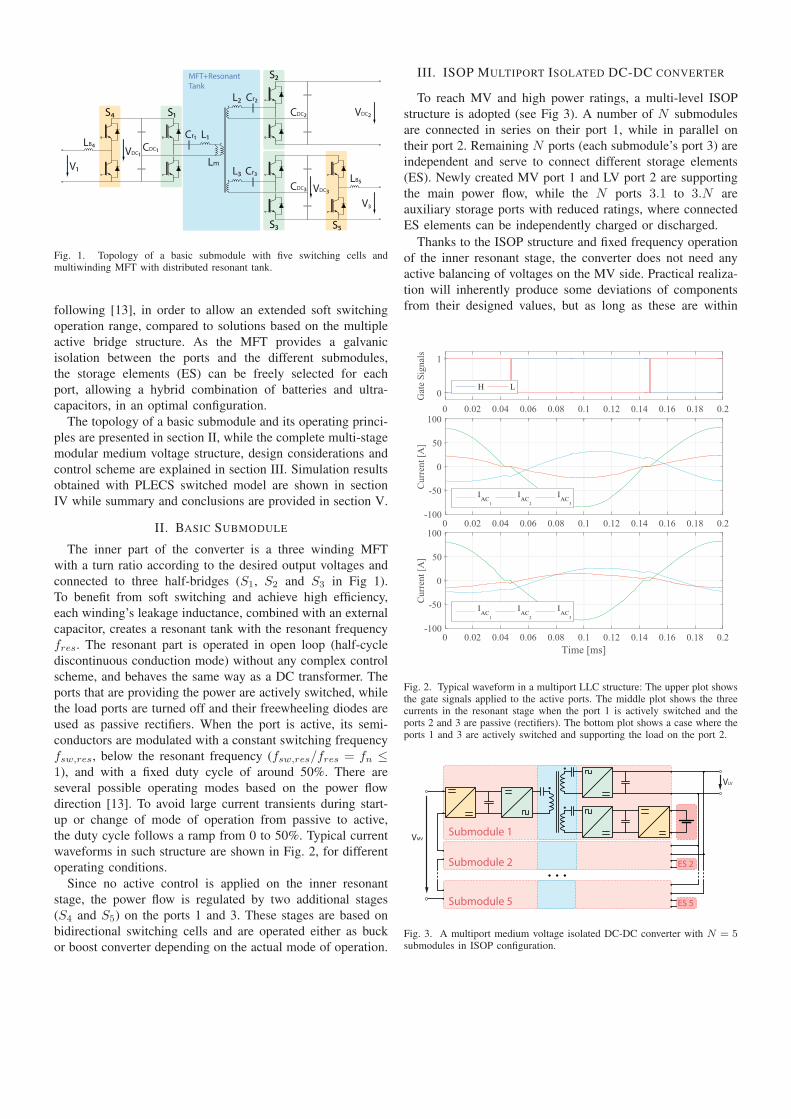
Fig. 1. Topology of a basic submodule with five switching cells andmultiwinding MFT with distributed resonant tank.
following [13], in order to allow an extended soft switching
operation range, compared to solutions based on the multiple
active bridge structure. As the MFT provides a galvanic
isolation between the ports and the different submodules,
the storage elements (ES) can be freely selected for each
port, allowing a hybrid combination of batteries and ultra-
capacitors, in an optimal configuration.
The topology of a basic submodule and its operating princi-
ples are presented in section II, while the complete multi-stage
modular medium voltage structure, design considerations and
control scheme are explained in section III. Simulation results
obtained with PLECS switched model are shown in section
IV while summary and conclusions are provided in section V.
II. BASIC SUBMODULE
The inner part of the converter is a three winding MFT
with a turn ratio according to the desired output voltages and
connected to three half-bridges (S1, S2 and S3 in Fig 1).
To benefit from soft switching and achieve high efficiency,
each winding’s leakage inductance, combined with an external
capacitor, creates a resonant tank with the resonant frequency
fres. The resonant part is operated in open loop (half-cycle
discontinuous conduction mode) without any complex control
scheme, and behaves the same way as a DC transformer. The
ports that are providing the power are actively switched, while
the load ports are turned off and their freewheeling diodes are
used as passive rectifiers. When the port is active, its semi-
conductors are modulated with a constant switching frequency
fsw,res, below the resonant frequency (fsw,res/fres = fn ≤1), and with a fixed duty cycle of around 50%. There are
several possible operating modes based on the power flow
direction [13]. To avoid large current transients during start-
up or change of mode of operation from passive to active,
the duty cycle follows a ramp from 0 to 50%. Typical current
waveforms in such structure are shown in Fig. 2, for different
operating conditions.
Since no active control is applied on the inner resonant
stage, the power flow is regulated by two additional stages
(S4 and S5) on the ports 1 and 3. These stages are based on
bidirectional switching cells and are operated either as buck
or boost converter depending on the actual mode of operation.
III. ISOP MULTIPORT ISOLATED DC-DC CONVERTER
To reach MV and high power ratings, a multi-level ISOP
structure is adopted (see Fig 3). A number of N submodules
are connected in series on their port 1, while in parallel on
their port 2. Remaining N ports (each submodule’s port 3) are
independent and serve to connect different storage elements
(ES). Newly created MV port 1 and LV port 2 are supporting
the main power flow, while the N ports 3.1 to 3.N are
auxiliary storage ports with reduced ratings, where connected
ES elements can be independently charged or discharged.
Thanks to the ISOP structure and fixed frequency operation
of the inner resonant stage, the converter does not need any
active balancing of voltages on the MV side. Practical realiza-
tion will inherently produce some deviations of components
from their designed values, but as long as these are within
0 0.02 0.04 0.06 0.08 0.1 0.12 0.14 0.16 0.18 0.20
1
Gat
e Si
gnal
s
H L
0 0.02 0.04 0.06 0.08 0.1 0.12 0.14 0.16 0.18 0.2-100
-50
0
50
100C
urre
nt [A
]
IAC
1
IAC
2
IAC
3
0 0.02 0.04 0.06 0.08 0.1 0.12 0.14 0.16 0.18 0.2Time [ms]
-100
-50
0
50
100
Cur
rent
[A]
IAC
1
IAC
2
IAC
3
Fig. 2. Typical waveform in a multiport LLC structure: The upper plot showsthe gate signals applied to the active ports. The middle plot shows the threecurrents in the resonant stage when the port 1 is actively switched and theports 2 and 3 are passive (rectifiers). The bottom plot shows a case where theports 1 and 3 are actively switched and supporting the load on the port 2.
ES 2
ES 5
Submodule 1
VLV
VMV
Submodule 2
Submodule 5
Fig. 3. A multiport medium voltage isolated DC-DC converter with N = 5submodules in ISOP configuration.
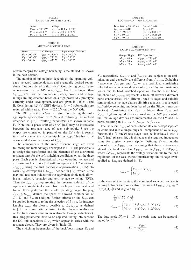
TABLE IRATINGS AT CONVERTER LEVEL
Power VoltagePMV = 500 kW VMV = 10 kV ± 20%PLV = 500 kW VLV = 750 V ± 20%PES = 100 kW VES = 300 V ± 33%
TABLE IIRATINGS AT SUBMODULE LEVEL
Power DC Voltage Input/Output VoltageP1 = 100 kW VDC1
= 2500 V V1 = 2000 VP2 = 100 kW VDC2 = 750 V V2 = 750 VP3 = 20 kW VDC3
= 450 V V3 = 300 V
certain margins the voltage balancing is maintained, as shown
in the next section.
The number of submodules depends on the operating volt-
ages, selected semiconductors and eventually desired redun-
dancy (not considered in this work). Considering boost nature
of operation on the MV side, VDC1has to be bigger than
VMVmax/N . For the simulation studies, power and voltage
ratings are implemented based on a high power MV prototype
currently under development, and are given in Tables I and
II. Considering 4.5 kV IGBT devices, N = 5 submodules are
required with a rated VDC1= 2.5 kV on the MV side.
The DC capacitors CDCiare sized considering the volt-
age ripple specification of 2.5% and following the method
described in [12]. Resulting parameters are shown in table
IV. Note that a phase-shift of 2π/N [rad] may be introduced
between the resonant stage of each submodule. Since the
output are connected in parallel on the LV side, it results
in a reduction of the voltage ripple on VLV . This has to be
considered during the sizing of CDC2 .
The components of the inner resonant stage are sized
following the methodology developed in [13]. The principle is
to design the transformer and the elements of the distributed
resonant tank for the soft switching conditions on all the three
ports. Each port is characterized by an operating voltage and
a maximum load modelled with an equivalent AC resistance
Rac1,2,3 , using the first harmonic approximation (FHA). To
each Rac corresponds a Lrmax , defined in [12], which is the
maximal resonant inductor of the equivalent single tank allow-
ing an inductive behavior and zero voltage switching (ZVS).
Then the Lequ1,2,3, representing the resonant inductor of the
equivalent single tanks seen from each port, are evaluated
for all three ports and the whole operating range. Keeping
Lequ ≤ Lrmax defines the space of allowed combination of
L1, L2 and L3. In addition, further criteria on the Lequ can
be applied in order to refine the selection of L1,2,3, for instance
keeping Lequ the closest possible to Lopt1,2,3 , as defined
in [12], or some criteria linked to the physical realization
of the transformer (minimum realizable leakage inductance).
Resulting parameters have to be adjusted, taking into account
the DC link capacitors CDCiwhich appear in series with the
resonant circuit. They are given in Table III.
The switching frequencies of the buck/boost stages S4 and
TABLE IIILLC RESONANT TANK PARAMETERS
Turn Ratio = 250:75:45 Lm =3.1mHfsw,res = 5kHz fn = 0.95L1 = 41.00 μH Cr1 = 22.81 μFL2 = 3.69 μH Cr2 = 283.21 μFL3 = 7.40 μH Cr3 = 130.00 μF
TABLE IVDC LINK CAPACITORS PER PORT
Voltage Ripple DC CapacitorsΔV1 = 63 V CDC1
= 250 μFΔV2 = 20 V CDC2
= 500 μFΔV3 = 12 V CDC3 = 620 μF
S5, respectively fsw,MV and fsw,ES , are subject to an opti-
mization and generally are different from fsw,res. Switching
frequencies fsw,MV and fsw,ES are optimized considering
selected semiconductor devices of S4 and S5 and switching
losses due to hard switched operation. On the other hand,
the choice of fsw,res represents a trade-off between different
ports characterized with different rated voltages and suitable
semiconductor voltage classes (limiting analysis to a selected
half-bridge switching modules based on the Silicon semicon-
ductors). Considering that VDC1is higher than VDC2
and
VDC3, high-voltage devices are used on the MV ports while
the low-voltage devices are implemented on the LV and ES
ports, resulting in fsw,MV ≤ fsw,res ≤ fsw,ES .
The inductors LB4.iof each submodule can be kept separate
or combined into a single physical component of value LB4.
Further, the N buck/boost stages can be interleaved with a
2π/N [rad] phase shift, which reduces the required inductance
value for a given current ripple. Defining VDCtot as the
sum of all the VDC1.i, and assuming that these voltages are
almost identical, one has VDCtot= N(VDC1
+ ΔVDC1),
where ΔVDC1represents the voltage variation due to the load
regulation. In the case without interleaving, the voltage levels
applied to LB4 are defined in (1).
VLB4=
{VMV − VDCtot
VMV
(1)
In the case of interleaving, the combined switched voltage is
varying between two consecutive fractions of VDCtot(x1, x2 ⊂
[1, 2, 3, 4, 5]) and is given by (3).
x1
N≤ D′
4 ≤ x2
N(2)
VLB4=
{VMV − x1(VDC1
+ΔVDC1)
VMV − x2(VDC1+ΔVDC1
)(3)
The duty cycle D′4 = 1−D4 in steady state can be approxi-
mated by (4)
D′4 =
VMV
VDCtot
(4)
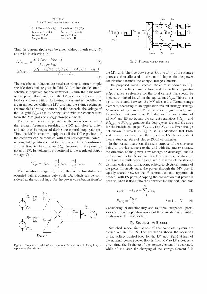
TABLE VBUCK/BOOST STAGES PARAMETERS
Buck/Boost MV (S4) Buck/Boost ES (S5)fsw,MV = 1 kHz fsw,ES = 10 kHzΔIMV = 5 A ΔIES = 2 ALB4
= 10 mH LB5= 5 mH
Thus the current ripple can be given without interleaving (5)
and with interleaving (6).
ΔIMVwo =D′
4(VMV − VDCtot)
fsw,MV LB4
(5)
ΔIMVwi=
(D′4 − x1/N) · (x2(VDC1
+ΔVDC1)− VMV )
fsw,MV LB4
(6)
The buck/boost inductors are sized according to current ripple
specifications and are given in Table V. A rather simple control
scheme is deployed for the converter. Within the bandwidth
of the power flow controller, the LV grid is considered as a
load or a source with a fluctuating power and is modelled as
a current source, while the MV grid and the storage elements
are modeled as voltage sources. In this scenario, the voltage of
the LV grid (VLV ) has to be regulated with the contributions
from the MV grid and energy storage elements.
The resonant stage is operated in the open loop close to
the resonant frequency, resulting in a DC gain close to unity,
and can thus be neglected during the control loop synthesis.
Thus the ISOP structure imply that all the DC capacitors of
the converter can be modeled with their series/parallel combi-
nations, taking into account the turn ratio of the transformer
and resulting in the capacitor C ′equ (reported to the primary)
given by (7). Its voltage is proportional to the regulated output
voltage VLV .
C ′equ = CDC1
+n22
n21
CDC2+
n23
n21
CDC3(7)
The buck/boost stages S4 of all the four submodules are
operated with a common duty cycle D4, which can be con-
sidered as the control input for the power contribution from/to
VMV
V’ES1-5
V’LV
D4
D5.1-5.5
LB4
L’B5
C’equ
I’LV
I’ES1-5
IMV
S4
S5.1-5.4
Fig. 4. Simplified model of the converter for the control. Everything isreported to the primary.
V*LV
VLV
PIPIPI
PI
I*LV P*LV
P*MV
P*ES1
P*ES5
VES1
VMV
I*MV
I*ES1
I*ES5
IES5
IES1
VES5
D4
D5.1
D5.5
+ +
+
+
-
-
-
-
IMV
EMS
SoC1-5
VLV
IMV
IES1
IES5
Fig. 5. Proposed control structure
the MV grid. The five duty cycles D5.1 to D5.5 of the storage
ports are then allocated to the control inputs for the power
contributions from/to the energy storage elements.
The proposed overall control structure is shown in Fig.
5. An outer voltage control loop and the voltage regulator
PIVLVgives a reference for the total current that should be
injected or sinked into/from the equivalent Cequ. This current
has to be shared between the MV side and different storage
elements, according to an application related strategy (Energy
Management System - EMS), in order to give a reference
for each current controller. This defines the contribution of
all MV and ES ports, and the current regulators PIIMVand
PIIES1to PIIES5
generate the duty cycles D4 and D5.1−5.5
for the buck/boost stages S4.1−4.5 and S5.1−5.5. Even though
not shown in details in Fig. 5, it is understood that EMS
system receives data from the respective ES elements about
their status (eg. state of charge (SoC) of batteries).
In the normal operation, the main purpose of the converter
being to provide support to the grid with the energy storage,
the direction of the power flow (charge or discharge) should
be the same for the N submodules. Nevertheless, the structure
can handle simultaneous charge and discharge of the storage
element with some restrictions, related to electrical ratings of
the ports. In steady-state, the power through the MV port is
equally shared between the N submodules and supported (if
needed) with ES ports. Adopting the convention that power is
positive when it flows into the converter (at any port) one has:
PMV = −PLV −N∑i=1
PESi (8)
PMVi=
PMV
Ni = 1, ..., N (9)
Considering bi-directionality and multiple indepedent ports,
various different operating modes of the converter are possible,
as shown in the next section.
IV. SIMULATION RESULTS
Switched mode simulations of the complete system are
carried out in PLECS. The simulation shows the operation
of the voltage control loop for the LV side (VLV ) at half of
the nominal power (power flow is from MV to LV side). At a
given time, the discharge of the storage element 1 is activated,
while 40 ms later, the charging of the storage element 2 is

10
20
30I M
V[A
]
-300
-250
-200
I LV[A
]
-50
0
50
I ES1-
5[A]
2450
2550
VD
C1[V
]
740
760
VD
C2[V
]
10 50 90 130
440
460
Time [ms]
VD
C3[V
]
(a)
-30
-20
-10
I MV
[A]
200
250
300
I LV[A
]
-50
0
50
I ES1-
5[A]
2450
2550
VD
C1[V
]
740
760
VD
C2[V
]
10 50 90 130
440
460
Time [ms]
VD
C3[V
]
(b)
Fig. 6. At t = 10 ms, the storage discharge current IES1is increased from 0 to 60 A, at t = 50 ms, the charge current IES3
is increased from 0 to -40 Aand at t = 90 ms, the load/source current through the LV port is increased from 200 A to 300 A. VDC2
is regulated to 750V while the VDC1.iare adapted
in order to supply the power requested by the low voltage port. In (a) the main power is flowing from the MV port to the LV port while it is reversed in (b).In both cases, cross regulation is visible on the VDC3.i
.
2500
2510
VD
C1[V
]
01020304050
I MV
[A]
2500
2510
VD
C1[V
]
0 1 2 3 4 50
1020304050
Time [ms]
I MV
[A]
Fig. 7. The voltage ripple on the DC capacitors of each port 1 (VDC1.1−5)
and the IMV current ripple with (upper two plots) and without (lower twoplots) interleaving of the buck/boost stages of the MV side. To illustrate bettercurrent ripple improvement, the simulation with interleaving is done with aninductor LB4
= 10 [mH] and the simulation without interleaving with aLB4 = 200 [mH].
-80
0
80
I AC
1[A]
740
750
760
VD
C2[V
]
-80
0
80
I AC
1[A]
0 0.2 0.4 0.6 0.8 1
740
750
760
Time [ms]
VD
C2[V
]
Fig. 8. The resonant current in each port 1 (IAC1.1−5) and the ripple on
the output voltage VDC2 , with (upper two plots) and without (lower twoplots) interleaving of the resonant LLC stages.

10 20 30 40 50 60 70 80Time [ms]
2460
2480
2500
2520
2540V
DC
1 [V]
Fig. 9. Multiple DC link voltages on the MV side are shown, before and afteran artificially introduced deviation of the resonant tank elements from theirdesigned values is introduced. After t = 10 ms, the value of L1 and Cr1 ofthe submodule 2 have been increased by +20% while after t = 30 ms, thevalue of L1 and Cr1 of the submodule 4 have been decreased by -20%. Theresults show a consequent offset of less than 1% on the voltage (and thus thepower), but no instability, and the converter continues to operate normally.
activated, followed by load increase of the LV side. This
scenario is somewhat arbitrarily chosen in order to demonstrate
the independent operation of the storage port of the different
submodules, while the voltage regulation is done through the
boost stage of the MV port. An overview of the complete
sequence is shown in Fig. 6a, while the same sequence but
with a reversed power flow between the MV and the LV port
is shown in Fig. 6b.
The effects of the interleaving of the buck/boost stages on
the MV side and the interleaving the LLC resonant stages
are shown in Fig. 7 and Fig. 8, respectively, with further de-
scription provided in captions. Finally, the effect of deviations
of the resonant tank elements from their designed values, on
the voltage balancing on the MV side is illustrated in Fig. 9.
It is reasonable to expected that deviations of the resonant
tank elements can be maintained with ±20% deviations from
desired values.
V. CONCLUSION
This paper presents the topology of a multiport medium
voltage DC-DC converter. It is based on the ISOP combination
of multiple identical submodules, each comprising an open-
loop operated resonant stage, and closed-loop operated regu-
lation stages on two out of three ports. In this way, conversion
tasks have been clearly separated between voltage adaptation
and galvanic isolation done with inner resonant stage and
control realized with regulation stages. The operating modes of
the converter have been described and a simple control scheme
is proposed, allowing for full bi-directionality and power
flow control. The converter is characterized with multiple
auxiliary ports which are made available for the connection
of LV energy storage elements, that can be freely mixed
in terms of different technologies (e.g. ultra-capacitors and
batteries). Thus, flexible and easily scalable grid supporting
solutions can be realized, both in terms of power and energy.
Furthermore, the presented topology allows further extensions
for higher operating voltages by increasing the number of
submodules connected in series (MFT insulation must be takeninto account and will directly depend on the system operating
voltage) or higher power with paralleling at the submodule or
converter level.
REFERENCES
[1] F. Mura and R. De Doncker, “Design aspects of a medium-voltage directcurrent (mvdc) grid for a university campus,” in Power Electronics andECCE Asia (ICPE ECCE), 2011 IEEE 8th International Conference on,May 2011, pp. 2359–2366.
[2] M. Liserre, T. Sauter, and J. Hung, “Future energy systems: Integratingrenewable energy sources into the smart power grid through industrialelectronics,” Industrial Electronics Magazine, IEEE, vol. 4, no. 1, pp.18–37, March 2010.
[3] H. Tao, A. Kotsopoulos, J. Duarte, and M. Hendrix, “Family of mul-tiport bidirectional dc-dc converters,” Electric Power Applications, IEEProceedings -, vol. 153, no. 3, pp. 451–458, May 2006.
[4] C. Zhao, S. D. Round, and J. W. Kolar, “An isolated three-portbidirectional dc-dc converter with decoupled power flow management,”IEEE Transactions on Power Electronics, vol. 23, no. 5, pp. 2443–2453,Sept 2008.
[5] H. Tao, A. Kotsopoulos, J. Duarte, and M. Hendrix, “Transformer-coupled multiport zvs bidirectional dc-dc converter with wide inputrange,” Power Electronics, IEEE Transactions on, vol. 23, no. 2, pp.771–781, March 2008.
[6] S. Falcones, R. Ayyanar, and X. Mao, “A dc-dc multiport-converter-based solid-state transformer integrating distributed generation and stor-age,” Power Electronics, IEEE Transactions on, vol. 28, no. 5, pp. 2192–2203, May 2013.
[7] Z. Pavlovic, J. A. Oliver, P. Alou, O. Garcia, and J. A. Cobos,“Bidirectional multiple port dc/dc transformer based on a series resonantconverter,” in Applied Power Electronics Conference and Exposition(APEC), 2013 Twenty-Eighth Annual IEEE, March 2013, pp. 1075–1082.
[8] H. Krishnaswami and N. Mohan, “Constant switching frequency seriesresonant three-port bi-directional dc-dc converter,” in Power ElectronicsSpecialists Conference, 2008. PESC 2008. IEEE, June 2008, pp. 1640–1645.
[9] W. Chen, X. Ruan, H. Yan, and C. Tse, “DC-DC conversion systemsconsisting of multiple converter modules: Stability, control, and experi-mental verifications,” Power Electronics, IEEE Transactions on, vol. 24,no. 6, pp. 1463–1474, June 2009.
[10] D. Dujic, C. Zhao, A. Mester, J. Steinke, M. Weiss, S. Lewdeni-Schmid,T. Chaudhuri, and P. Stefanutti, “Power electronic traction transformer-low voltage prototype,” Power Electronics, IEEE Transactions on,vol. 28, no. 12, pp. 5522–5534, Dec 2013.
[11] S. Moury and J. Lam, “Modular isolated high frequency medium voltage(mv) step-up resonant dc/dc converters with high-gain rectifier forwind energy systems,” in 2015 IEEE Energy Conversion Congress andExposition (ECCE), Sept 2015, pp. 4789–4796.
[12] Y. K. Tran and D. Dujic, “A multiport isolated dc-dc converter,” in 2016IEEE Applied Power Electronics Conference and Exposition (APEC),March 2016, pp. 156–162.
[13] Y. K. Tran, D. Dujic, and P. Barrade, “Multiport resonant dc-dcconverter,” in Industrial Electronics Society, IECON 2015 - 41st AnnualConference of the IEEE, Nov 2015, pp. 003 839–003 844.