a mos model for computer-aided design - … bound... · an improved mos model for computer-aided...
TRANSCRIPT
R938 Philips Res. Repts 31,71-83,1976
A MOS MODEL FOR COMPUTER-AIDED DESIGN
by F. M. KLAAS SEN
AbstractAn improved MOS model for computer-aided design techniques hasbeen proposed, which fairly represents some physical effects that arebecoming more manifest in devices manufactured with modern technol-ogy. Arguments for the proposed representation are supported bycomparing experimental and simulated results.
1. Introduetion
The design of large and complicated MOS integrated circuits can best beachieved by means of computer-aided design techniques. At the present timeseveral MOS transistor models are available for the circuit designer. As anexample we mention: Model SPICE 1),which, despite the use of very elementaryequations (ideal square-law behaviour), has proved to be adequate for model-ling simple p-channel MOS circuits; Model FETSIM 2), which takes moreaccurate account of substrate effects on the current, and is therefore moresuitable for non-square-law behaviour as found in n-channel MOS or com-plementary MOS circuits.Although the last model is one of the most accurate models published sofar,
several effects have been modelled unsatisfactorily, in partienlar saturationeffects of the de current and the drain conductance in saturation. Moreover incommon with all published models, the description of the active gate-channelcapacitances is poor. For instance, in contradiction to practice, the gate-draincapacitance does not reduce to zero when the transistor is driven to saturation.In high-tolerance designs this shortcoming will certainly be masked by parasiticand stray capacitances, but is not acceptable in self-aligned densily packedcircuits.
In the model presented here the shortcomings mentioned above have beeneliminated by improved description of several physical effects. This model hasbeen incorporated in a circuit-analysis package for some time and is frequentlyused.
2. D.e. Model
2.1. Basic I-V relationIn a practical MOS structure the total charge per unit area induced in the
substrate consists of a mobile charge in the surface inversion layer and a fixedcharge in the underlying depletion region, due to ionized impurities. Since the
f3ID = - [f(VG, Vs) - f(VG' VD)],
2(1)
72 F. M. KLAASSEN
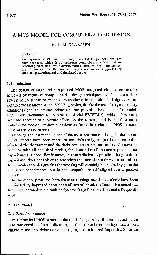
latter quantity is a function of the substrate potential (fig. I), a four-terminalI-Vrelation exists 2.4.5). From all published results we prefer here to reproducethe relations given by Meyer 2), since they illustrate clearly that the MOST maybe considered as a symmetrical device with respect to source and drain.
Bulk contact
Fig. LA MOS structure.
Relating the voltages of source (Vs), gate (VG) and drain (VD) to the substratethe drain current (ID) is given by
where
(2)
VTX is a constant,
# Box Wf3= ,
Lhox(3)
and
(4)
In these equations # is the mobility in the inversion layer, B is the dielectricconstant, N is the substrate doping and (/JF is the bulk Fermi potential. For thegeometry symbols W, Land hox we refer to fig. 1. Equations (1) and (2) are onlyvalid for
(5)
and
(6)
A MOS MODEL FOR COMPUTER-AIDED DESIGN 73
When in an n-channel device VD > VS, VTS is the wellknown threshold voltage,which separates the passive mode (ID = 0) from the active mode. On the otherhand eq. (6) separates the linear active region from the saturation region. LetVSAT be the drain voltage at which saturation occurs, then eq. (6) yields forVG = VTO
[le (le
2 )tJ2VSAT = -2rpF + -2' + """""4 + VG- VTX + 2rpF (7)
For not too short channels eq. (1) may be used in the saturation region(VD;;?; VSAT) by substituting the value of VSAT for the variable VD· WhenVD< Vs the transistor operates in the inverse mode.Equation (1)remains valid;only the meaning of VTS and VTD has to be interchanged.Although from a viewpoint of physics eq. (1) is the more correct 1- V relation,
some models prefer to use a simpler j-function than eq. (2). This approach isjustified by the near-square-law behaviour of ID(Va), which often is found inp-channel transistors in saturation. A link between this approach and eq. (1)and (2) can easily be made by substituting eq. (5) in eq. (6) which determinesVSAT' One then obtains
VG - VTS (VSAT + 2rpF)t - (Vs + 2rpF)t--- = 1+ le ----------VSAT - Vs VSAT - Vs
(8)
In practice the quotient that multiplies le varies between 0.5 (for low values ofVG) and 0.3. Therefore relation (8) suggests a reasonable proportionality be-tween the saturation value VDS. SAT = VSAT - Vs and the effective gate voltageVa - VTS, in particular for low values of le (low substrate doping). This givessome background to the simple semi-empirical current relation used in somemodels 1)
(9)
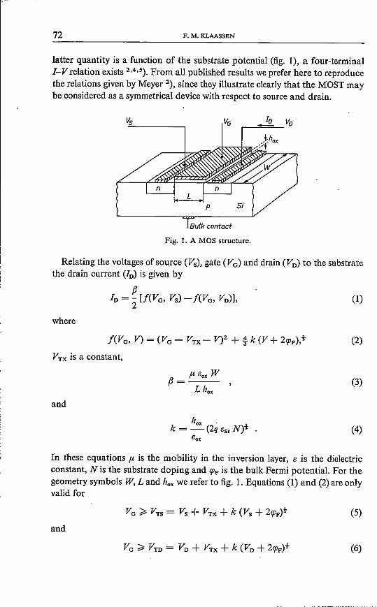
For Vos -4- c5(VG- VTS) eq. (9) gives the correct square-law behaviour. With aparameter-determining method 3) to be described later we have observed that(9) can represent reasonably measured I-V characteristics for le-values notexceeding 1, although the accuracy is less than for eqs (1) and (2). For instance,when the average error between measured characteristics and eq. (1) and eq.(2) is 3% for le = 1 (compare fig. 2), eq. (9) produces already an error of 10%.Generally, for le > 1, the accuracy with eq. (9) is poor and moreover deter-mination of parameters becomes a very time-consuming affair.
2.2. Channel length modulation
As discussed above, the basic I-V relations (1)- (4) will show perfect satura-tion (dIo/dVo = 0) behaviour for VD > VSAT' However, in practice the outputconductance is by no means zero (compare fig. 2). This conductance is generally
(10)
74 F. M. KLAASSEN
2.2
p-MOSTVSB=OVro=-1·60VK =0.63{Jo = 7.5pA/V2.8, =0.010582 =0.00658J =0a./L=0.125
ID(mA) 1.6
t
1.
2.0
1.0
4
°O~-2~~4--~6--~8~~W~----------
-VOS
Fig. 2a Measured and simulated (fully drawn curve) I-V characteristic of p-channel MOST(W= IOO(J.m,L = 5 urn) .
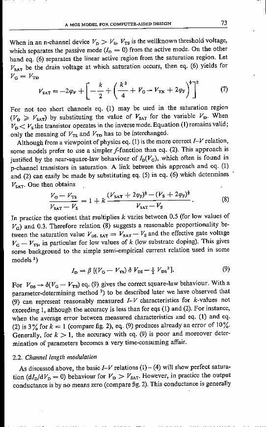
attributed to two feedback mechanisms. The first one 6) is due to a spreading ofthe depletion region near the drain, which results in a reduction of the activechannel length. The second mechanism 7) by which a change in drain voltagecan affect the drain current is by charge induction in the channel from fieldlines emanating from the drain diffusion region. Meyer has suggested modellingthe saturation behaviour by using the approximation
Jos = JDs, SAT (1 + v Vos),
where Jos, SAT is given by eqs (1) and (2).However, the constant output conductance found from this relation dis-
agrees with experimental results 8) and also with numerical results 9) obtainedfrom solving a two-dimensional Poisson equation. Both results indicate thatthe saturated output conductance varies in proportion to (VD - VSAT)-t. Theeasiest way to incorporate this behaviour in the previous equations is to use avoltage-dependent channel length
A MOS MODEL FOR COMPUTER-AIDED DESIGN 75
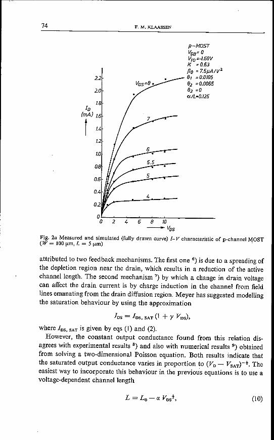
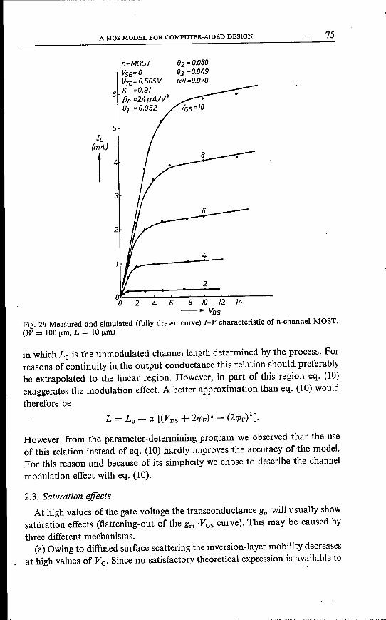
n-MOST (}2 =0.060Vsa=O (}3 =0.049Vro=0.505V a/L=0.070
6 K =0.91/10 =24j1A/V2
(}I =0.052
5ID
(mA)
14
,;
2r,
4I
IlV
2
00 2 4 6 e 10 12 14
-VDS
Fig. 2b Measured and simulated (fully drawn curve) I-V characteristic of n-channel MOST.(W = 100 (.lm, L = 10 (.lm)
in which Lo is the unmodulated channellength determined by the process. Forreasons of continuity in the output conductance this relation should preferablybe extrapolated to the linear region. However, in part of this region eq. (10)exaggerates the modulation effect. A better approximation than eq. (10) wouldtherefore be
However, from the parameter-determining program we observed that the useof this relation instead of eq. (10) hardly improves the accuracy of the model.For this reason and because of its simplicity we chose to describe the channelmodulation effect with eq. (10).
2.3. Saturation effectsAt high values of the gate voltage the transconductance gm will usually show
saturation effects (flattening-out of the gm-VGS curve). This may be caused bythree different mechanisms.
(a) Owing to diffused surface scattering the inversion-layer mobility decreasesat high values of VG. Since no satisfactory theoretical expression is available to
(11)
76 F. M. KLAASSEN
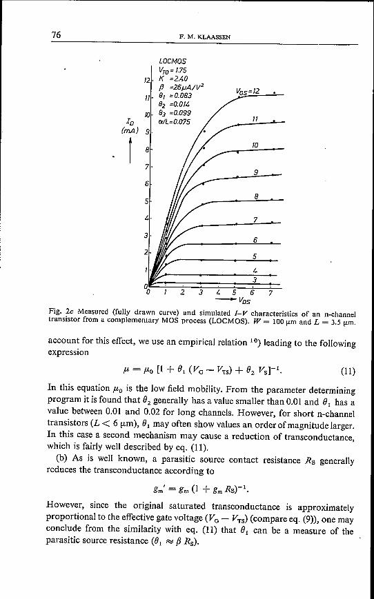
LOCMOSVro= T.75
T2 K =2.40fJ =26j.JA/V2 VGs=T2
11 81 =0.08382 =0.OT4
TO 83 =0.099Io rx/L=0.075
(mA) 9
fTO8
79
6
85
2 3 4 5 6 7-VOS
Fig. 2e Measured (fully drawn curve) and simulated I-V characteristics of an n-channeltransistor from a complementary MOS process (LOCMOS). W = 100 fLmand L = 3.5 urn.
7
6
5
43
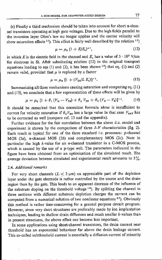
account for this effect, we use an empirical relation 10) leading to the followingexpression
In this equation #0 is the low field mobility. From the parameter determiningprogram it is found that 82 generally has a value smaller than 0.01 and 81 has avalue between 0.01 and 0.02 for long channels. However, for short n-channeltransistors (L < 6 [Lm),81may often show values an orderofmagnitudelarger.In this case a second mechanism may cause a reduction of transconductance,which is fairly well described by eq. (11).
(b) As is well known, a parasitic source contact resistance Rs generallyreduces the transconductance according to
However, since the original saturated transconductance is approximatelyproportional to the effective gate voltage (VG - VTS) (compare eq. (9)), one mayconclude from the similarity with eq. (11) that 81 can be a measure of theparasitic source resistance (81 I':::i fJ Rs).
A MOS MODEL FOR COMPUTER-AIDED DESIGN 77
(c) Finally a third mechanism should be taken into account for short n-chan-nel transistors operating at high gate voltages. Due to the high fields parallel tothe inversion layer Ohm's law no longer applies and the carrier velocity wiIlshow saturation effects 11). This effect is fairly well described by the relation 12) .
(12)
in which E is the electric field in the channel and Ec has a value of 5 . 103V/cmfor electrons in Si. Aftër substituting relation (12) in the original transportequations leading to eqs (1) and (2), it has been shown 13) that eq. (1) and (2)remain valid, provided that # is replaced by a factor
(13)
Summarizing all three mechanisms causing saturation and comparing eq. (11)and (13), we conclude that a fair representation of these effectswill be given by
# = #0 [1 + B1 (Vo - YTS) + B2 VSB + B3 (VD - VS)]-l. (14)
It should be remarked that this correction formula alone is insufficient tocorrect for velocity saturation if B3 VDS has a large value In that case VSAT hasto be corrected as well (compare ref. 13 and the appendix).
Further evidence for the fair correlation between the above d.c. model andexperiment is shown by the comparison of three 1- V characteristics (fig. 2).Each result is typical for one of the three standard i.C. processes: p-channelMOS (2a), n-channel MOS (2b) and complementary MOS (2e). Note inparticular the high k-value for an n-channel transistor in a C-MOS process,which is caused by the use of a p-type well. The parameters indicated in thefigure have been obtained from an optimization of the simulated result. Theaverage deviation between simulated and experimental result amounts to 3%.
2.4. Additional remarksFor very short channels (L <; 3 fLm)an appreciable part of the depletion
layer under the gate electrode is rather controlled by the source and the drainregion than by the gate. This leads to an apparent decrease of the influence ofthe substrate doping on the threshold voltage 14). By splitting the channel inthree sections with different substrate depletion charges the current can becomputed from a numerical solution of two nonlinear equations 15). Obviouslythis method is rather time-consuming for a general purpose circuit program.However, since very short structures are preferably made by ion implantationtechniques, leading to shallow drain diffusions and much smaller k-values thanin present structures, the above effect can become less important.
In some applications using short-channel transistors, the drain current nearthreshold has an exponential behaviour far above the drain leakage current.This so-called subthreshold current is essentially a diffusion current of minority
78 F. M. KLAASSEN
carriers from the source, which are injected by surface band bending. Althoughmodels exist to describe this current 16.17) for reason of simplicity these equa-tions are not included in a general circuit program. Moreover, measures canbe taken (e.g. the application of a fixed source-substrate bias) to reduce theeffects to an acceptably low value.
3. Dynamic model ..3.1. Free-carrier charge
When the gate voltage of a MOS transistor is suddenly increased, it takessome time before an increased drain current is observed. An extra charge ofmajority carriers therefore has to be built up in the channel region. A represen-tation of this and other time dependent effects in MOS transistors is given infig. 3 by the inclusion of capacitances or their corresponding charges. All
BFig. 3. A dynamic MOS model.
elements are related to the physical structure of the device and will be discussedin this section.To include the active channel charge in the scheme of fig. 3 nearly all models
use two lumped capacitors Coo and Cas, which are derived by differentiatingthe total free carrier charge Qr with respect to Vas and Voo 2). For reasons ofsimplicity the charge Qr of an ideal MOS has always been taken, i.e. a devicein which the substrate depletion charge is neglected. Denoting
the expressions for Qr and the capacitances can be written in a form
A MOS MODEL FOR COMPUTER-AIDED DESIGN 79
(15)
( V12
)C =J.-C 1-----GO , 3 ox (V
l+ V
2)2 .
In these equations Cox is the gate-channel capacitance. The weakness of thisapproach becomes manifest in the saturation mode. In contradiction toexperimental results, CGSand eGO according to eq. (16) do not drawnearvaluesof 2/3 and 0, respectively, when VD -+ VSAT• In many conventional circuits,where parasitics dominate, this shortcoming does not introduce large deviationsof delay time. However, in more modern structures, in which parasitics arereduced by ion implantation techniques, LOCOS oxydation and use of siliconon saphire, eqs (15) and (16) are no longer acceptable.
Unfortunately when the substrate charge is taken into account the expressionfor the free channel charge Qc becomes very complicated 18). This leads toexpressions for the capacitances which are not acceptable for a general circuitanalysis program. A simpler modelling of Qc is therefore needed. Surprisinglyeq. (15) can be used for this purpose, provided that the definition of the symbolV2 is changed, Using the definitions
(16)
VI = (VG- Vs- VTS)
V2 = (Vo - VD - VTD),(17)
where VTD is given in eq. (6), the expression (15) for Qc is very close to theexact result. This has been illustrated in fig. 4 in a case of rather high substratedoping. Since V2 becomes °when VD approaches VSAT, Qc in agreement withpractice becomes independent of VD. Also, when eq. (17) is substituted in thecapacitance expressions, eqs (16) are close to experimental behaviour.
Although, as appears from the above, a dynamic model with capacitanceexpressions that satisfy both accuracy and simplicity, can be made, it isadvantageous for some general purpose programs to operate with chargesinstead of capacitances. The reason for this is that charges are more smoothfunctions of time than capacitances, which leads to minor problems in numer-ical procedures.
In order to meet this need, the charge Qc has to be split in a part Qcs control-led by the source-gate voltage, and a part QfD controlled by the gate-drainvoltage. Unfortunately this split cannot be made by strict computation fromphysics; only the total free charge can be computed. However, arguing thatQrs and Qro should exactly correspond to the capacitances eGS and COD'respectively, the following simple expressions can be given:

80 F. M. KLAASSEN
1.0 k = 1- exact--- modelled
Ïjj
...t 0.75o~~
f ::5°o~--~~~~--~~~~-----0.25 0.5 0.75 1.0
-VD/VSAT
Fig. 4. The total free-carrier charge as a function of Vos and Vos.
(18)
[VI V2 ]QfD f>.:::i i Cox V2 - •
VI + V2
When VD approaches VSAT' these expressions satisfy the practical result thatQrs and QfD approach a value of t Cox (VGS - YTS) and 0, respectively, andno longer change in saturation. However, comparing eqs (18) and (19) with eq.(15) one will observe that for low values of VDS the sum of Qrs and QfD is lowerthan the charge Qr. Although this difference is incorrect from the physical pointof view, we did not observe any appreciable effect on the delay time of aninverter, when the above intrinsic dynamic MOS model was used or a modelwith capacitances according to eqs (16) and (17).
(19)
3.2. Bulk charge
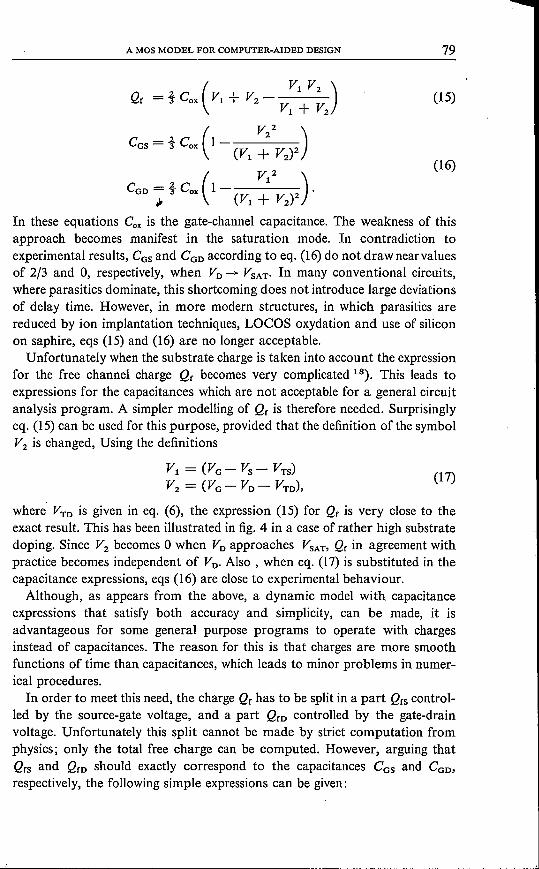
In the same way as for the free-carrier charge, the charge in the substratedepletion layer may be computed 18). Again the expressions are very com-plicated. Generally the bulk charge changes little because of the screeningaction ofthe channel. However, in the subthreshold region, where the inversionlayer disappears, this changes drastically, as can be observed from a familiarC-V plot. Again, an exact description of the dependence of the gate-substratecapacitance (CGB) on the gate voltage VG is extremely complicated 19). Propermodelling of this behaviour is therefore essential. We have done this along thelines sketched in fig. 5, where an exact C-V plot is given together with the model-ling result. In this way we use the expression (for VFB ~ VG ~ VTO)
[VG- VFB VTO- VG]
CGB = Cox W L 0.15 + ----VTO - VFB VTO - VFB
(20)
A MOS MODEL FOR COMPUTER-AIDED DESIGN 81
)(
(JO
"Cl]cJ 0.8
t0.6
0.1,
0.2 ::VFBOL---~~----~~--------
-exact- --- modelled
-VGB
Fig. 5. The exact and modelled gate-bulk capacitance.
which corresponds to an approximation of the gate-bulk charge
[(VG - VFB)2 (VG - VTO)2 - (VTQ- VFB)2]
QOB = Cox WL 0.075 --------VTO - VFB 2 (VTO - VFB)
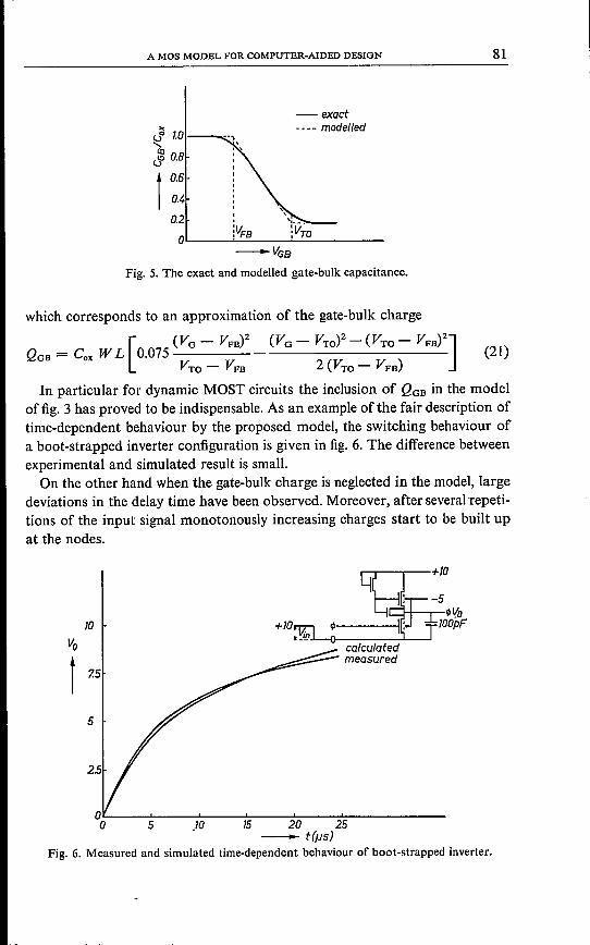
In particular for dynamic MOST circuits the inclusion of QOB in the modelof fig. 3 has proved to be indispensable. As an example of the fair description oftime-dependent behaviour by the proposed model, the switching behaviour ofa boot-strapped inverter configuration is given in fig. 6. The difference betweenexperimental and simulated result is small.On the other hand when the gate-bulk charge is neglected in the model, large
deviations in the delay time have been observed. Moreover, after severalrepeti-tions of the input signal monotonously increasing charges start to be built upat the nodes.
(21)
+TO
-5~lIa
TO TOOpF
Va
t 7.5
5
)0 15 20 25-- ttus)
5
Fig. 6. Measured and simulated time-dependent behaviour of boot-strapped inverter.

82 F. M. KLAASSEN
3.3. Parasitic charges
In many integrated MOS circuits the switching speed is limited by the timetaken to charge the many stray capacitors rather than to charge the intrinsicchannel. These parasitic capacitors include wiring capacitance between inter-connections and the substrate, gate-to-source and drain-overlap capacitance,and the voltage-dependent capacitor of the source and drain areas. All thesecapacitors or their corresponding charges also have been included in thescheme of fig. 3, which represents a dynamic MOS model. We will not discussthe modelling of these para sitics here, since this has been done before.
Conclusion
To meet the need for a simple, sufficiently accurate transistor model forcomputer-aided circuit simulation of MOS integrated circuits, an improvedmodel as shown in fig. 3 has been proposed. These improvements are necessaryfor devices which, due to technological progress, require a better description ofeffects such as drain conductance or velocity saturation, and also a betterrepresentation of the intrinsic free-carrier charge.
The essential relations describing all parts of the model except the parasiticcomponents are given by eqs (1), (2), (3), (4), (10), (14), (17), (18), (19) and (21).
Support for optimal representation of some physical effects as given by theabove equations has been obtained from direct comparison of measuredcharacteristics and simulated results. The final result is shown in fig. 2.
dID I- =0.dVo VD=V'SAT
(22)
Acknowledgements
The.author wishes to express his gratitude to Dr. F. Berz, Dr. P. A. Hart andMr. E. Kleihorst for many helpful discussions, to Mr. L. Nederlof for providingthe results of the bootstrapped inverter and to Dr. G. Roman for his contri-bution to correct the saturation voltage.
Eindhoven, December 1975
Appendix
When eq. (14) is substituted in the current eq. (1) a corrected value for thesaturation voltage V/SAT may be obtained from the condition 13)
Unfortunately this condition leads to a quartic equation in VD. Therefore wetry a first-order approximation. Defining
A MOS MODEL FOR COMPUTER-AIDED DESIGN 83
where the original VSAT satisfies the conditionf'(VsAT) = 0 (compare eq. (2»,the condition (22) leads to
03 [f(V/SAT) - j(Vs)] +f' (V/SAT) = O. (23)1+ 01 (Va - VT) + {)z Vs + 03 (V/SAT- Vs)
When 6. may be considered as only a correction to VSAT>thej-functions in (23)may be expanded and we obtain
(24)
in which
[ k (kZ )-!J-1j"(V)=-2-k -2+ 4+ Vo-V.rx+2CPF . (25)
Now the corrected saturation voltage V/SATis given by eqs (7) and (24).
REFERENCE1) D. A. Hodges and H. Schichman, IEEE J. solid-state Circ. SC-3, 285, 1968.2) J. E. Meyer, RCA Rev. 32, 42, 1971.3) F. M. Klaassen, W. de Groot and F. L. v, d. Markt, next paper.4) C. T. Sah and H. C. Pao, IEEE Trans. EI. Dev. EO-13, 393, 1966.5) J. A. v, Nielen and O. W. Memelink, Philips Res. Repts 22,35,1967.6) C. T. Sah and V. K. G. Reddi, IEEE Trans. EI. Dev. EO-12, 139, 1965.7) S. R. Hofstein and G. Warfield, IEEE Trans. EI. Dev. EO-l2, 129, 1965.8) O. Frohman-Bentchkovski, IEEE Trans. EI. Dev, EO-I6, 108, 1969.9) J. E. Schroeder and R. S. Muller, IEEE Trans. EI. Dev. EO-IS, 954,1968.
10) N. Murphy, F. Berz and 1. Flinn, Solid St. Electr. 12, 775, 1969.11) E. J. Ryder, Phys. Rev. 90, 766, 1953.12) F. N. Trofimenkoff, Proc. IEEE 53,1765,1965.13) F. M. Klaassen, IEEE Trans. EI. Dev. ED-I7, 858, 1970.14) V. L. Rideout a.o., IBM J. Res. Dev. 19, 10, 1975.15) L. O. Yau, EI. Letts 11, 450, 1975.16) M. B. Barron, Sol. St. Electr. 15, 293, 1972.17) R. R. Troutman, IEEE J. solid-state Circ. SC-9, 55, 1974.18) R. S. C. Cobbold, Theory and application of field effect transistors, WHey,NewYork,
1970, p. 274.19) S. M. Sze, Physics of semiconductor devices,WHey,New York, 1969,p. 432.20) L. Nederlof, private communication.