a mobile data acquisition system
TRANSCRIPT

A mobile data acquisition system
Article (Published Version)
http://sro.sussex.ac.uk
Anderson, K, Arabidze, G, Blumenschein, U, Da Silva, P, Dotti, A, Schlager, G, Schlereth, J, Solov'yanov, O, Teuscher, R and Vivarelli, I (2007) A mobile data acquisition system. Journal of Instrumentation, 2. P07002. ISSN 1748-0221
This version is available from Sussex Research Online: http://sro.sussex.ac.uk/id/eprint/49405/
This document is made available in accordance with publisher policies and may differ from the published version or from the version of record. If you wish to cite this item you are advised to consult the publisher’s version. Please see the URL above for details on accessing the published version.
Copyright and reuse: Sussex Research Online is a digital repository of the research output of the University.
Copyright and all moral rights to the version of the paper presented here belong to the individual author(s) and/or other copyright owners. To the extent reasonable and practicable, the material made available in SRO has been checked for eligibility before being made available.
Copies of full text items generally can be reproduced, displayed or performed and given to third parties in any format or medium for personal research or study, educational, or not-for-profit purposes without prior permission or charge, provided that the authors, title and full bibliographic details are credited, a hyperlink and/or URL is given for the original metadata page and the content is not changed in any way.

This content has been downloaded from IOPscience. Please scroll down to see the full text.
Download details:
IP Address: 130.88.99.231This content was downloaded on 26/07/2014 at 08:59
Please note that terms and conditions apply.
A mobile data acquisition system
View the table of contents for this issue, or go to the journal homepage for more
Home Search Collections Journals About Contact us My IOPscience

2007 JINST 2 P07002
PUBLISHED BY INSTITUTE OF PHYSICS PUBLISHING AND SISSARECEIVED: May 23, 2007REVISED: June 29,2007ACCEPTED: July 5, 2007
PUBLISHED: July 11, 2007
A mobile data acquisition system
K. Anderson,a G. Arabidze,b U. Blumenschein,c P. Da Silva,d A. Dotti,e G. Schlager, fJ. Schlereth,g O. Solov’yanov,h R. Teuscheri and I. Vivarellie∗aUniversity of Chicago,5640 South Ellis Avenue, Chicago, Illinois 60627-1433, U.S.A.bUniversity of Athens,Panepistimiopouli, Zografou, 15771 Athens, GreececInstituto de Fisica de Altas Energias (IFAE), Universidad Autonoma de Barcelona,Facultat de Ciencies-Edifici Cn, 08193 Bellaterra (Barcelona), Spain
dUniversidade Federal do Rio de Janeiro (UFRJ),Ilha Do Fundao, 21945-970 Rio de Janeiro, BrazileIstituto Nazionale di Fisica Nucleare (INFN), Università degli Studi di Pisa,Edificio C - Polo Fibonacci Largo B. Pontecorvo, 3, 56127 Pisa, Italyf CERN, 1211 Genève 23, Switzerland, andTechnical University of Vienna,Atominstitut der österreichischen Universitäten Stadionallee 2, 1020 Vienna, AustriagArgonne National Laboratory (ANL),9700 South Cass Avenue, Argonne, IL 60439, U.S.A.hState Research Center of Russian Federation, Institute for High Energy Physics (IHEP)st. Pobedy 1, Protvino, 142281 RussiaiCanadian Institute of Particle Physics (IPP), University of Toronto,60 Saint George St., Toronto, ON, CanadaE-mail: [email protected]
ABSTRACT: A mobile data aquisition (MobiDAQ) was developed for the ATLAS central hadroniccalorimeter (TileCal). MobiDAQ has been designed in order to test the functionalities of the TileCalfront-end electronics and to acquire calibration data before the final back-end electronics were builtand tested. MobiDAQ was also used to record the first cosmic ray events acquired by an ATLASsubdetector in the underground experimental area.
KEYWORDS: Front-end electronics for detector readout; Control and monitor systems online.
∗Corresponding author.
c© 2007 IOP Publishing Ltd and SISSA http://www.iop.org/EJ/jinst/

2007 JINST 2 P07002
Contents
1. Introduction 1
2. The tile calorimeter 2
3. Requirements 2
4. System setup 34.1 MobiDAQ hardware components 4
4.1.1 Digital readout 54.1.2 Analog readout 64.1.3 Communication 64.1.4 The trigger system 6
4.2 External components 6
5. MobiDAQ software 85.1 Diagnostic tests 85.2 Automation of the test procedure 135.3 Performance of the diagnostic tests 14
6. Data taking with MobiDAQ 146.1 Performance 146.2 Data taking with cosmic rays 15
7. Conclusions 16
1. Introduction
In March 2004 the first eight of sixty-four modules of the TileCal barrel cylinder were loweredinto the experimental cavern and barrel modules were added on a regular base. At that time, boththe final back-end TileCal electronics and the TileCal Low Voltage Power Supplies (LVPS) werenot ready to be used. Thus there was a long time span with electronically fully-equipped TileCalmodules in the ATLAS cavern without adequate readout and power systems installed.
The TileCal collaboration decided to exploit this time period by building a temporary dataacquisition system which could check the integrity of the electronics and verify the functionalitiesof many TileCal modules together.
A very important issue for the commissioning of the detector was to test modules in a config-uration as similar as possible to the final configuration in ATLAS. In this way problems could befound and solved at an early stage of the commissioning.
– 1 –

2007 JINST 2 P07002
2. The tile calorimeter
The central part of the ATLAS hadronic calorimeter system [1] uses scintillating tiles as activematerial. The tiles are arranged in an iron structure, perpendicular to the beam axis. They are readout by two wave length shifting fibers (WLS), on either side of the tile. TheWLS fibers are groupedtogether in order to reach the desired granularity and their signal is read by HAMAMATSU R7877PMTs (an 8-stage version of the R5900 [2]) located on the front-end electronics.
The front-end electronics of each TileCal module are located on its external edge. Each modulecontains two so-called superdrawers. Each houses up to 48 PMT’s and the associated analog anddigital electronics. A sketch of the electronics can be found in figure 1. The signal from the PMTis collected on a 3-in-1 card [3], which shapes the pulse and then sends it to:
- The trigger summation cards (the adders), where the signals from a calorimeter tower arecollected and summed up. The signal is then used for the trigger decision.
- The integrator. Each TileCal superdrawer is equipped with an integrator, which is used forcalibration purposes and for minimum bias monitoring.
- Two different amplifiers whose relative gain is 64. The output of the amplifiers is then sentto the digitizer boards for digitization. In each superdrawer there are 8 digitizer boards. Eachdigitizer board provides a double sampling (one for each of the two gains) using two separate10-bit fast ADCs. The sampled signal is then stored in the pipelines, waiting for the triggerdecision.
The 3-in-1 card can also inject a known amount of charge in the TileCal electronics chain. This isthe so-called CIS (Charge Injection System), and it has been designed for calibration purposes.
Once the trigger signal is received, the corresponding data are sent to the back-end electronicsfor further processing.
Two systems are used to communicate with TileCal: the Timing, Trigger and Control(TTC [4]) system and the CANbus [5]. The TTC is an optical signal transmission system usedto distribute timing, trigger and control information (accepted triggers, event count, resets, config-uration, test commands, etc.) to the front-end electronics. This information is sent by the LHCmachine, the Level-1 Central Trigger Processor, the Data Acquisition System and the DetectorControl System. There is a wide span of components that build the TTC system starting from theTTC-VMEbus interface module (TTCvi) and going via encoders (TTCex), transmitters and opticalcouplers (TTCoc) to receivers (TTCrx [6]). A similar optical system is used to read out the datafrom the pipelines once the trigger is received by the front-end electronics. The CANbus system isused for the communication with the integrator and with the High Voltage system. One CANbusdaisy chain spans 16 superdrawers.
The total number of TileCal readout channel is about 104. At present, TileCal is under com-missioning in the ATLAS experimental cavern.
3. Requirements
Addressing all of the constraints presented above, a new test-bench was developed and namedMobiDAQ [7] (Mobile Data Acquisition system). The two main tasks of MobiDAQ were:
– 2 –

2007 JINST 2 P07002
Figure 1. Sketch of the TileCal electronics (one superdrawer). In the figure, ROD (ReadOut Driver) indi-cates the back-end electronics system responsible for the data reading from the superdrawers.
• Running diagnostic tools for testing the TileCal electronics, cabling and connections.
• Performing real data acquisition (calibration, cosmic ray muons, etc.).
The system is designed to be an independent, mobile DAQ system for the simultaneous readoutof up to eight superdrawers (∼ 6% of the TileCal barrel). The commissioning strategy of TileCaland the environment in the ATLAS cavern defined the main requirements of MobiDAQ.
• Mobility is essential for a temporary system which has no fixed place inside the cavern. Ithas to be possible to move it to different places without interfering with ongoing work.
• It has to be an independent DAQ system, parallel to the TileCal back-end. In this way we arenot only able to start commissioning TileCal modules independently of other timescales butwe also develop a system that can later cross-check the results from the TileCal back-end.
• The full readout chain has to be checked. The electronics has to be certified with cables offinal length. The MobiDAQ system has to be able to test final services like cables, opticalfibers, low voltage supplies, etc. as soon as they are available.
• The software developed for the new test-bench has to be based on the ATLASDAQ software,allowing an easy integration in the final TileCal DAQ.
4. System setup
The main components of MobiDAQ are installed in a mobile rack, shown in figure 2. It houses aVME crate with different electronic boards (five single board PCs, one TTCvi, one TTCex, four
– 3 –

2007 JINST 2 P07002
Figure 2. The MobiDAQ system. The mobile rack houses most of the components. The lowest crate inthe rack is the NIM crate, which provides the trigger logic for the data acquisition. In the middle the VMEcrate is installed and in the upper part the custom trigger conversion boards are placed. The laptop, which isstanding on the top of the rack, is used as the interface to the system.
Charge to Digital converter boards), a NIM crate, which provides the trigger for the data acquisitionand custom trigger conversion boards. Other components like power supplies for the CANbus orfor the TileCal superdrawers are either located close to the rack or close to the TileCal modules.
The schematic MobiDAQ layout is shown in figure 3. The data flow is indicated with thearrows. The G-Link and the Trigger cables are used for readout whereas the TTC fibers areused to send commands to the superdrawers. The CANbus is a special case because it worksbi-directionally. Power supplies and the external interface are not included in the scheme.
4.1 MobiDAQ hardware components
MobiDAQ is based on VP110 [8] boards from the company Concurrent Technologies. They areVME processor boards, supporting a 800 MHz processor and a variety of interfaces including anoption for an on-board hard disk drive. In total five VP110 boards are used, one equipped with ahard disk and used to control the other four boards and to store the processed data. The function
– 4 –

2007 JINST 2 P07002
Figure 3. The layout of the MobiDAQ system. The schematic view shows how the system was intercon-nected with the TileCal superdrawers.
of the other four boards is to gather and process the digitized data from the superdrawers. All fiveVP110 boards are installed inside a VME crate and connected via Ethernet cables to a networkHUB for communication.
4.1.1 Digital readout
The digitized data from the superdrawer are sent via the G-LINK optical fibers to to the VP110board, which is equipped with two ODIN cards (Optical Dual G-Link S-LINK interface) each inorder to receive the information.
The S-LINK is a simple data link which is based on the S-LINK specifications defined atCERN [9]. It is used to connect the front-end electronics to the next layer of readout electronics. Inaddition it also includes error detection, self-test functionality and a return channel for flow controland for return line signals.
The ODIN card [10] is a standard S-LINK implementation. It uses optical transceivers withduplex LC connectors for the optical transmission. The SSP card is a PCI mezzanine card which isused as an interface between S-LINK Destination Cards (in the MobiDAQ case ODIN cards) anda PMC environment (in the MobiDAQ case the VP110 boards).
The firmware of the ODIN card has been modified to include CRC checking. An overflowprotection is implemented to allow high rate triggering of the drawer (see section 5.1). Eventsare randomly sampled at a lower rate consistent with the processing speed available. This allowstesting of the drawer at the ATLAS maximum trigger rate of about 100 kHz.
– 5 –

2007 JINST 2 P07002
The data coming from the front-end electronics via S-LINK are then processed on the VP110board and finally stored on the hard disk.
4.1.2 Analog readout
Four analog-to-digital charge converters1 (QDC) are used for the readout of the analog signals fromthe adders. A trigger conversion card was developed to adapt the differential signal from the addersto the format and dynamic range of the QDCs.
4.1.3 Communication
As in the final TileCal setup, two systems are used to communicate with the superdrawer: the TTCand the CANbus systems.
In the VME crate a TTCvi and a TTCex module are installed. The TTCvi, configurablethrough VP110, sends signals to the TTCex, which converts the electrical signals into laser pulses.One of the ten optical outputs of the TTCex is used and connected via an optical fiber to an opticalsplitter (TTCoc in the following). Eight optical duplex fibers (TTC fibers) fan out from the TTCocand distribute the signals to the eight connected superdrawers.
To perform the readout and control the integrator ADC of many superdrawers connected viaseveral CANbus daisy chains, MobiDAQ was equipped with a Quadruple VME CANbus con-troller [11], the Readout Buffer. It is controlled by the VP110 boards. The Readout Buffer isspecially developed for the readout of TileCal. Its use in MobiDAQ made it possible to evaluate itin a real working environment and to give suggestions for improvements.
In addition to the readout of the integrator ADC, the ADC CANbus-Readout-Buffer chain isused as an alternate path to send commands to the 3in1 cards and provides the only path to readback settings from the 3in1 cards. As opposed to ATLAS, in MobiDAQ two of the four ReadoutBuffer ports are used to control the HV CANbus (sending commands to the HV micro cards andreading settings and values of the HV micro cards).
4.1.4 The trigger system
The trigger system of MobiDAQ is built with several NIM electronic modules (1). The modules aresituated in the NIM crate below the VME crate. The purpose of the logic is to provide the triggersignal (analogous to the ATLAS level 1 acceptance trigger signal) to the readout and issue “busy”signals, in order to disable the trigger while reading out the VME modules.
4.2 External components
Aside from the mobile rack there are several external components of the MobiDAQ system:
• User interface: although the VP110 boards can be used as an autonomous computer, a laptopor a PC is used as a user interface. It is connected to the network HUB via an Ethernet cableand the user can log in to all five VP110 boards if necessary. Nevertheless the processing ofthe data is all done on the boards themselves. By connecting the network HUB to an externalnetwork it is also possible to control MobiDAQ from any other computer terminal.
1Reference: CAEN QDC, Model V792
– 6 –

2007 JINST 2 P07002
Figure 4. One of the temporary low voltage power supplies which power the electronics of the TileCalmodule.
• CANbus power supply: close to the mobile rack there is a standard power supply to powerthe CANbus. It provides the 12 V for both CANbus lines.
• High voltage power supply: one of the final TileCal HV power supplies is used to power thesuperdrawers.
• Temporary low voltage power supplies (LVPS): commercial LVPS 2 are used to power thefront-end electronics. Their small size (20 × 25 × 7 cm) permits mounting them directly onthe TileCal fingers with specially designed aluminum plates as shown in figure 4. This min-imizes the impact of the MobiDAQ tests on the working environment close to the detector.
• Temporary cabling: eight full sets of temporary cables are routed from MobiDAQ to theTileCal modules. They are chosen to match the real ATLAS cable length, both on A and Cside. A set of cables includes the following parts:
– TTC fiber– G-Link fiber– Trigger cable– Laser fiber– HV cable– CANbus cable
Only one CANbus cable is needed for the eight superdrawers since they are connected toeach other via a CANbus daisy chain.
2Reference: Power-One Model ESP6C212265-00
– 7 –

2007 JINST 2 P07002
• Cooling: to ensure stable running conditions the front-end electronics have to be cooled. Thisis done with demineralized water at 18◦C. Two TileCal prototype cooling units are used; bothof them work with a ’Leak-less Cooling System’ [12].
The MobiDAQ rack, the laptop, the CANbus power supply and the HV power supply are alllocated inside the cavern, USA15. This cavern is separated by a 2 m concrete wall from the maincavern, UX15, where the ATLAS detector is installed. USA15 is equipped with many rows of racksto provide space for all the back-end electronics of the ATLAS subdetectors.
The temporary LVPS are located in UX15, attached to the fingers of the TileCal modules. Alsothe prototype cooling units are located in UX15, close to the detector.
5. MobiDAQ software
The software for MobiDAQ is based on several sources:
• The environment and libraries provided by the ATLAS Trigger and DAQ group [13].
• Readout libraries and test software developed in former test-beams.
• Test software used during the construction phase of the calorimeter.
In order to achieve the goals of MobiDAQ, not only significant changes and upgrades of theexisting software were necessary but also new code had to be developed. Libraries to access theVME modules, tests to perform detailed checks of the electronics, and the control of the paralleltests to prevent conflicts during data acquisition were the most significant pieces of code developed.
5.1 Diagnostic tests
The task of the diagnostic tests is to check very specific functionalities of a component or a set ofcomponents of the front-end electronics. The tests can be run in command-line mode or via theautomation system (see section 5.2).
At the end of a test the result is displayed, which is either “success” or “failure”. Additionalerror messages give hints about the type of problem that occurred. In the more sophisticated testsraw data or plots are saved into files for further analysis.
The tests are described in detail below.
ADC CANbus. The communication with the integrator ADC via CANbus is tested by retriev-ing the version number of its firmware. When the version number is received successfully theconnection is considered to be working.
TTC connection. This test checks the communication with the 3-in-1 cards via the optical TTCfibers. The bits of the 3-in-1 card are flipped in a distinct order and read back to verify the connec-tion and the functionality of the cards.
BCID (Bunch Crossing Identifier) test. The analog signal from the 48 channels of one TileCalsuperdrawer is digitized in 8 digitizer boards, which house the 10-bit fast ADC. Each digitizerboard contains two custom chips (TileDMU) that collect the information from 3 channels. EachTileDMU sends a BCID number with every event. The consistency of the BCID numbers all alongthe superdrawer is checked: they have to be identical for all TileDMUs.
– 8 –

2007 JINST 2 P07002
CRC (Cyclic Redundancy Check) test. The electronics in the superdrawer calculate a checksum using a specified formula and the measured data. The same procedure is performed outsidethe superdrawer with the received data and the two numbers are compared. If they are identical thetransmission of the data was successful.
Test of the Integrator readout chain. This test checks the functionality of the Integrator ADCand its communication with the back-end electronics. For each PMT channel, it additionally checksthe level of the pedestal and its RMS, the switching between the six integrator gains and the linearityof the signal. For this purpose the test is separated into two parts:
- The Integrator ADC test verifies the basic functionalities of the integrator ADC and the con-nection with the back-end via CANbus. A successful result in this test is essential to be ableto continue with the second test. In several steps the following points are verified:
– The initialization procedure.
– The configuration of subtracted pedestal and delay.
– The configuration of the 3-in-1 cards via CANbus.
– The configuration and performance of the automated scan (calibration and gain test).
– The performance of the fast ADC conversion for the minimum bias readout.
- The Integrator gains test checks the calibration of the six integrator gains. For this purposea DAC ramp is performed for each gain in its appropriate range and the ADC counts aremeasured. For each measurement the average ratio between DAC value and measured ADCcounts of 100 events is computed. The gains are calculated by a linear fit of the ratio. Theresulting gain and the linearity of the fit are required to correspond to the range measuredwith a set of well-performing reference superdrawers.
Additional tests, based on a data sample with 100 events, measure the pedestal and thepedestal noise for each channel and each gain. The pedestal noise is required to be lowenough to allow a minimum bias monitoring in all cells. In order to ensure the selection ofthe correct card, an additional test injects different charges for even and odd channels andmeasures the response of each channel.
The results of the integrator gains test for gain-5 are shown in figure 5 for one representativesuperdrawer. For each channel the fitted gain, the !2 of the fit, the pedestal and the pedestalnoise are plotted. The red lines indicate acceptable values for a standard TileCal superdrawer.
Register test. In the superdrawer a number of registers can be changed via TTC commands. Thistest verifies the ability to modify their settings.
The following registers are verified by the test:
- Motherboard time: One register exists per motherboard. It controls the time of the chargeinjection with respect to the arrival of the TTC command.
- DSkew time: One of the two fine DSkew registers of the TTCrx on the digitizer controls thephase between the ADC sampling and the 25 ns clock.
– 9 –

2007 JINST 2 P07002
Figure 5. An example of the result display for the integrator gains test.
- Pipeline length: a register controls the pipeline length, which is the time between the physicssignal and the arrival of the trigger signal to the front-end electronics.
- Pedestal level: One register per digitizer controls the pedestal level.
- Capacitor and DAC level for the 3-in-1 cards: It controls which one of the two capacitorsand which charge is used for the charge injection.
The test is started on one superdrawer at a time. After reading the test settings from theconfiguration database, five charge injection events are acquired. The average time and amplitudeof the signal are computed. Then the motherboard times are changed by 30 ns, and five more eventsare acquired. The new averaged value for the time is compared to the old one, channel by channel.The test fails if the time difference for any channel deviates from the expected result. The sametechnique is used for the DSkew time and for the pipeline length.
For the pedestal level, five pedestal events are read out and the samples are integrated. Thepedestal is subsequently increased and another five events are read out. The difference between theaverage results of the integrals is then verified.
The last step is to inject predefined charges and to verify the resulting amplitude of the readoutsignal.
If any of the changes fails for any of the channels, the whole test fails.
Noise test. The electronic noise is one of the most important parameters of the detector. It canbe different for every channel, depending on the electronic cards and their activity and it can evenvary in time.
– 10 –

2007 JINST 2 P07002
Channel Number0 10 20 30 40 50
Channel Number0 10 20 30 40 50
Noi
se (R
MS)
0.4
0.45
0.5
0.55
0.6
0.65
0.7
Low Gain Noise
Channel Number0 10 20 30 40 50
Channel Number0 10 20 30 40 50
Noi
se (R
MS)
0.4
0.6
0.8
1
1.2
1.4
1.6
High Gain Noise
Figure 6. A typical result from the noise test. The RMS pedestal noise (in ADC counts) of all channels ofsuperdrawer LBA47 in the low and the high gain readout is shown.
Significant effort was invested into keeping the noise level in TileCal close to the design ex-pectations.
For the noise test, 1000 pedestal events are taken. Seven digitized samples are read out in bothgains from each channel. The noise is then calculated as the RMS of the seven samples and theaverage RMS over many events is computed. A typical result can be seen in figure 6. The pedestalnoise of all channels in one representative superdrawer for the low and the high gain is shown. Thevalues are consistent with what expected for a standard TileCal superdrawer. The channels 32, 33and 44 are not instrumented with PMTs and therefore show lower values.
The noise test can be performed also at a 100 kHz rate in combination with the BCID andCRC tests. This allows the cross check of the data taking stability at high frequency.
Charge injection test. The charge injection test makes use of the CIS (Charge Injection System).Two capacitors on the 3-in-1 card are used to inject well defined charges into all the readout chan-nels. This charge simulates a signal from the photomultiplier and is digitized and read out by theelectronics through the same chain as a particle signal.
For the test two different charges are injected, 5 pC for the high gain and 600 pC for the lowgain. A Gaussian is fitted to the measured pulse and the amplitude is evaluated. Then this amplitudeis compared with values from reference superdrawers.
– 11 –

2007 JINST 2 P07002
Time (ns)0 20 40 60 80 100 120 140 160
ADC
cou
nts
0
100
200
300
400
500
600
Time (ns)0 20 40 60 80 100 120 140 160
ADC
cou
nts
0
100
200
300
400
500
600
Time (ns)0 20 40 60 80 100 120 140 160
ADC
cou
nts
0
100
200
300
400
500
600
Time (ns)0 20 40 60 80 100 120 140 160
ADC
cou
nts
0
100
200
300
400
500
600
Figure 7. A typical output of the charge injection test. The pulse in four channels is shown. A Gaussian isfitted to the seven digitized samples.
A typical output from a successful test can be seen in figure 7. The CIS pulse in four channelsis shown. The plot shows the value of the ADC reading as a function of time (ns). The gaussian fitto the pulse shape is also shown. The amplitude, the mean value, the sigma and the !2 of the fit areconsistent with what expected for a standard TileCal superdrawer.
High Voltage system. A high voltage control program was developed based on the ReadoutBuffer and the CANbus connection to the superdrawer. The readout via the Readout Buffer is aMobiDAQ-specific feature. In ATLAS a dedicated CANbus controller currently being developedwill be used. The HV control program provides all of the basic functionalities to control and readout the high voltage parameters:
- to set and read the voltages applied on the PMTs,
- to read the temperature probes located inside the superdrawer,
- to read the input voltages from the low voltage power supply,
- to set the CANbus node numbers for the superdrawers (used for identification inside a CAN-bus branch).
In addition, the test provides a continuous monitoring of the voltages by periodically savingthe values to files for further analysis.
Trigger. There are two separate trigger outputs: the hadron trigger and the muon trigger. Theformer provides the analog sum of the analog signals coming from the TileCal pseudo-projectivetowers, the latter the signal from the cells of the outer longitudinal TileCal sampling. The objectiveof this test is to check that the LVL1 trigger chain is working properly. This chain is composed of
– 12 –

2007 JINST 2 P07002
Figure 8. The user interface of the Diagnostic Verification System of MobiDAQ.
the 3-in-1 cards, the adders, and cables (internal and external). The signal is integrated and readout by the QDCs.
- The hadron output test checks the output of all adders present in the superdrawer. First it ischecked if it is possible to enable and disable the trigger output of the 3-in-1 card. After thatthree different charges (70, 140, and 210 pC) are injected into each readout channel. A linearfit is applied to the measured ADC counts. If the fit is within a tolerance of 3%, the output isaccepted as being linear.
- The muon output test ensures that the muon output of the adders is working correctly. This isaccomplished by injecting a fixed charge of 7 pC and verifying that the output signal equalsthe value from a reference superdrawer within a 5% tolerance.
5.2 Automation of the test procedure
In order to be able to perform the diagnostic tests in a fast and user-friendly manner, we madeuse of a graphical user interface based on Java, the Diagnostic Verification System (DVS) [14].Developed for the TDAQ [15] certification, it is capable of starting, synchronizing and controllingdifferent processes. A few modifications permitted the use of DVS as a framework to control theTileCal diagnostic tests.
DVS uses the TDAQ configuration database, which stores all the necessary information aboutsubdetector components needed for the configuration and data acquisition. For MobiDAQ the data
– 13 –

2007 JINST 2 P07002
base additionally defines if a test can be performed in parallel on several superdrawers or only onone at a time.
The diagnostic tests are arranged in hierarchical order. Therefore the simple tests, e.g. theverification of the communication with the superdrawers, are performed first and eventually, incase all the previous tests are successful, the more sophisticated tests are started. DVS controls thissequence and provides information about the test result to the user. In case of failure an additionalerror output is displayed. An example of the user interface is shown in figure 8. On the left sidea list of connected superdrawers can be seen. Some of them were tested successfully, which isindicated by the green square in front of the superdrawer name. The right side shows the log file ofthe last performed test with detailed information about the test status.
It is not mandatory to run the full chain of tests on all superdrawers. A test of interest can bechosen and started for a specific superdrawer, an essential feature in case of errors and during thedetailed investigation of problems.
The implementation of the diagnostic tests into DVS is an essential step since this facilitatesthe integration into the final DAQ system of TileCal.
5.3 Performance of the diagnostic tests
The diagnostic tests implemented in MobiDAQ are meant to provide a fast response about thesuperdrawer functionalities. They have been developed for the commissioning, but they will bemaintained also for ATLAS as a fast (and reliable) tool to verify the front-end electronics.
The time needed to perform a complete check of 8 TileCal superdrawers is about 5 minutes.Tests involving the CANbus system (which is intrinsically slower than the TTC system and whichallow the test of only one channel at a time) are typically much longer than the tests of the digitalreadout (noise, charge injection, registers). The complete test of the digital readout alone takes lessthan 1 minute.
6. Data taking with MobiDAQ
With the TDAQ software installed on MobiDAQ it is possible to take calibration runs, i.e., dataacquisition runs using the ATLAS official data acquisition software infrastructure. They closelyimitate real ATLAS runs, although they contain pedestals, signals coming from the TileCal chargeinjection system, or signals coming from light injected on the PMTs surface using a LED system.
While the tests described above are meant to be used as a fast debugging tool for the calorime-ter, these runs are used both to monitor its long term stability and to compute the calibration con-stants for the electronics. The data are stored in raw data files and have to be reconstructed andanalyzed offline.
6.1 Performance
The MobiDAQ data taking is usually done with a trigger rate of 1 kHz. The typical size of oneevent in one superdrawer is about 1 kB. This means that the typical amount of data written on thedisk is 8 MByte/s. One calibration run usually consist of 10000 events.
The total amount of data stored during the commissioning phase with MobiDAQ is about200 GB.
– 14 –

2007 JINST 2 P07002
Figure 9. A view of a cosmic muon (yellow) crossing the TileCalorimeter (red).
6.2 Data taking with cosmic rays
In June 2005 a milestone for TileCal (and ATLAS) was reached: cosmic muons were recorded inthe ATLAS cavern using TileCal and the MobiDAQ readout. This was the first time that a LHCsubdetector, in its final position, recorded a particle [16].
The trigger was obtained asking the coincidence of a signal above threshold in a back-to-back pair of TileCal towers. A specific programmable board which receives the signals from thecalorimeter and checks the coincidence of the towers has been designed and built.
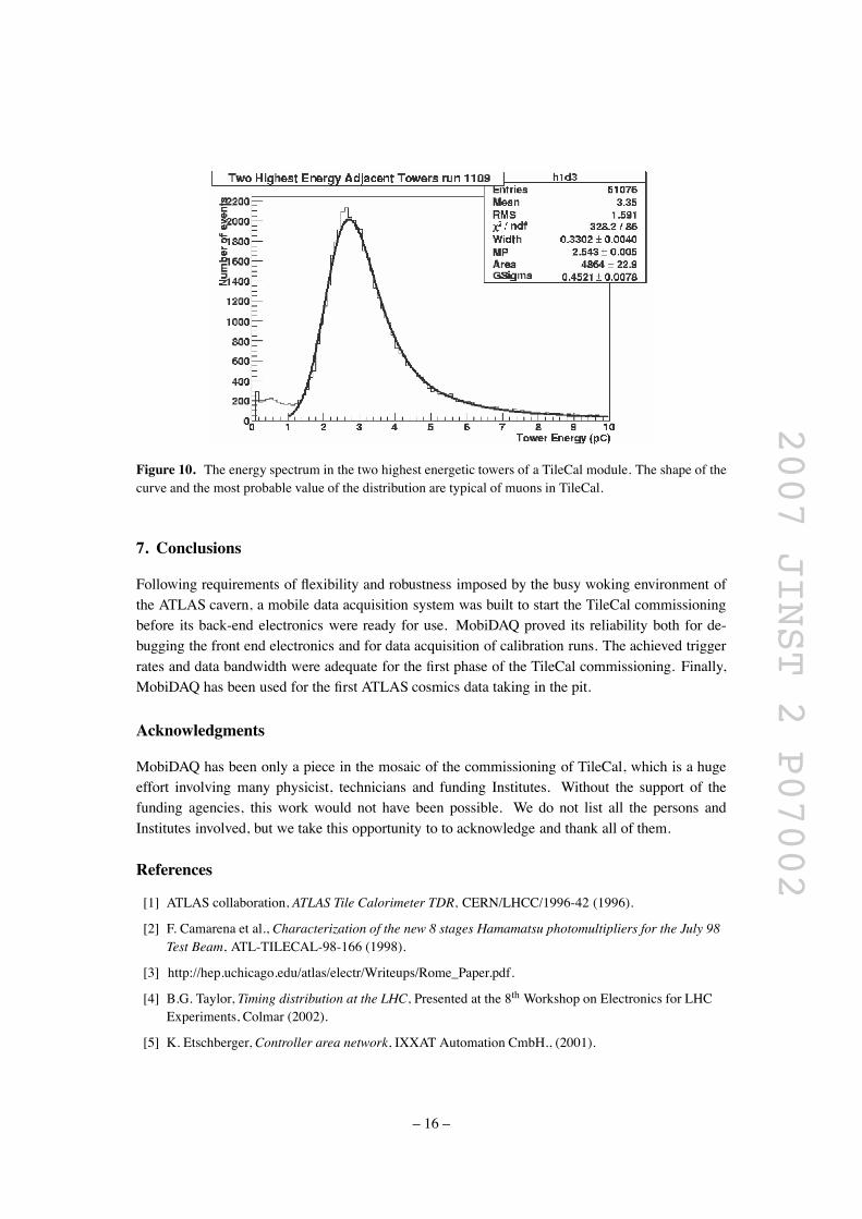
Figure 9 shows a view of one of the few thousands cosmic muons recorded. The yellowregions indicate a high energy deposit. The most probable value of the energy released in a TileCalmodule by a projective muon (with respect to the interaction point) is about 2.5GeV. That has to becompared with an average noise RMS per tower of about 50-60MeV. Figure 10 shows the energyspectrum in the two most energetic adjacent towers in a TileCal module. The histogram has beenfitted with a convolution of a Landau with a Gaussian function. The choice of the fitting functionhas been driven by studies done with test beams of muons. The most probable value is in a roughagreement with what is expected for muons.
– 15 –
2007 JINST 2 P07002
Figure 10. The energy spectrum in the two highest energetic towers of a TileCal module. The shape of thecurve and the most probable value of the distribution are typical of muons in TileCal.
7. Conclusions
Following requirements of flexibility and robustness imposed by the busy woking environment ofthe ATLAS cavern, a mobile data acquisition system was built to start the TileCal commissioningbefore its back-end electronics were ready for use. MobiDAQ proved its reliability both for de-bugging the front end electronics and for data acquisition of calibration runs. The achieved triggerrates and data bandwidth were adequate for the first phase of the TileCal commissioning. Finally,MobiDAQ has been used for the first ATLAS cosmics data taking in the pit.
Acknowledgments
MobiDAQ has been only a piece in the mosaic of the commissioning of TileCal, which is a hugeeffort involving many physicist, technicians and funding Institutes. Without the support of thefunding agencies, this work would not have been possible. We do not list all the persons andInstitutes involved, but we take this opportunity to to acknowledge and thank all of them.
References
[1] ATLAS collaboration, ATLAS Tile Calorimeter TDR, CERN/LHCC/1996-42 (1996).
[2] F. Camarena et al., Characterization of the new 8 stages Hamamatsu photomultipliers for the July 98Test Beam, ATL-TILECAL-98-166 (1998).
[3] http://hep.uchicago.edu/atlas/electr/Writeups/Rome_Paper.pdf.
[4] B.G. Taylor, Timing distribution at the LHC, Presented at the 8th Workshop on Electronics for LHCExperiments, Colmar (2002).
[5] K. Etschberger, Controller area network, IXXAT Automation CmbH., (2001).
– 16 –

2007 JINST 2 P07002
[6] J. Christiansen et al., TTCrx reference manual, Tech. Rep., RD12 project collaboration,CERN-EP/MIC (2003).
[7] G. Schlager, Energy response of the ATLAS calorimeter system, Ph.D. thesis, Technical University ofVienna (2006).
[8] Concurrent technologies webpage: http://www.gocct.com.
[9] H.V. der Bij et al., S-LINK, a data link interface specification for the LHC era, IEEE Nucl. Sci. Symp.Conf. Rec. 1 (1996) 465.
[10] http://www94.web.cern.ch/hsi/s-link/devices/odin/.
[11] http://www.ifae.es/Tilecal%5FElectronics/rb.htm.
[12] P. Bonneau et al., Cooling system for the TILECAL hadron calorimeter of the ATLAS detector,ATL-TILECAL-98-139 (1998).
[13] http://atlas.web.cern.ch/Atlas/GROUPS/DAQTRIG/Newdaqtrig_legacy.php.
[14] M. Barczyk, et al., Verification and diagnostics framework in ATLAS trigger, ATL-DAQ-2003-033(2003).
[15] ATLAS collaboration, ATLAS high-level trigger, data-acquisition and controls: Technical DesignReport, CERN-LHCC-2003-022 (2003).
[16] A. Wright, First “data” from LHC, Nature Physics, advanced online publication, 14 July 2005.
– 17 –