a method for charging and discharging capacitors in ... · a method for charging and discharging...
TRANSCRIPT

Fig. 1: Modular Multilevel Converter
Fig. 2: One cell of Modular Multilevel Converter
A Method for Charging and Discharging Capacitors in Modular Multilevel Converter
Anandarup Das, Hamed Nademi and Lars Norum
All the authors are with Department of Electric Power Engineering, NTNU, Trondheim, Norway. E-mails: [email protected], [email protected] and [email protected]
Abstract-In this paper, a method for charging and discharging capacitors in Modular Multilevel Converter (MMC) is explained. The proposed method helps to start the converter from a de-energized condition and does not require any auxiliary voltage source. An additional resistance is inserted in the MMC arm and by appropriately switching this resistance, both charging and discharging of the MMC cells can be accomplished. A theoretical background is presented for drives applications and design examples are included. Simulation and experimental results are included at the end to validate the proposed concept.
I. INTRODUCTION
The Modular Multilevel Converter (MMC) is one of the most attractive and promising multilevel converter topologies proposed in recent times [1-4]. There are many advantages of this converter over conventional ones [5-8]. The modular structure, low device ratings, easy scalability and a possibility of using redundant cells for fault tolerant applications are some of the key features of this converter. As such, the converter has found a commercial application within few years of its first proposal [9].
The MMC consists of a number of cells in series (Fig. 1). Each cell consists of two switches and a capacitor (Fig. 2) and acts as a two port device. When switch S1 is turned on, the capacitor is bypassed and the output voltage of the cell is zero. When S2 is turned on, the capacitor voltage is obtained at the output. With many cells connected in series, the output voltage of the converter is very smooth and requires no or very minimal filters to improve the output voltage quality.
In the present work, a method for charging the capacitors is proposed. The MMC consists of many capacitors in all the three phases, thus it is important to have a simple and reliable procedure to charge all of them. Some methods have already been proposed in literature for charging the series capacitors [1, 10, 11]. However, all of them rely on an external voltage source to do so. In this paper, the charging of the capacitors is done from the main voltage source. For this, an additional resistance is connected in series to the arms of each cell (Fig. 3). This resistance is controlled by a switch and is explained in details in the next section. The switch can be a mechanical or electronic one. But, since the switching frequency of this additional switch is very low and the switch is used only during charging and discharging process, a mechanical contactor can be used for this purpose. By appropriately
inserting or bypassing the resistance the capacitors in the cells can be charged to the desired voltage level. The resistance is also used if the capacitors need to be discharged, e.g. during the removal of the cell from the circuit. At steady state operation, the resistance is bypassed from the circuit.
In the following section the basic idea behind the circuit operation is presented. This is followed by the development of the theory needed for designing the resistance values. Some simulation results are presented that shows the charging procedure for one leg of the converter. A small laboratory setup has been built and one experimental result has been included to show the effectiveness of the proposed method.
978-1-61284-971-3/11/$26.00 ©2011 IEEE 999

(a) (b)
Fig. 3: Simultaneous charging of four capacitors in one phase; (a) top arm (b) bottom arm.
(a) (b)
Fig. 4: Charging circuit for top two cells in one arm.
II. CIRCUIT OPERATION
In the present concept, the capacitors in the cells of MMC are charged from the main voltage source. For drives application, the main voltage source consists of the dc bus formed by the rectifier system. Fig. 3(a) shows one phase of the converter connected to the dc bus. Assume in Fig. 3(a) that the top and bottom arms of the phase have four cells each. For normal operation of the converter, it is required that all the capacitors are pre-charged to a voltage of Vdc/4 [1]. It is assumed that initially all the capacitors are discharged and the load is disconnected. Switches SC1 and SC2 are open; hence the resistances RC1 and RC2 are present in the circuit. In the following discussion, Smn denotes the name of a switch in a cell where 'm' stands for the cell number (m=1 to 8) and 'n' denotes the switch in each cell (n=1 or 2).
In order to charge all the capacitors in the upper arm, Si1 (i=1 to 4) are turned on. The complementary switches Si2 (i=1 to 4) are turned off. Simultaneously, the switches Si2 (i=5 to 8) in the lower arm are turned on. This forms a series RLC circuit fed from a dc source. As such, the capacitors in the top arm all charge to Vdc/4, where Vdc is the dc bus voltage. The charging current dies down to negligibly small amount once the charging process is over. After this, the switches Si1 (i=1 to 4) are turned off and Si1 (i=5 to 8) in the lower arm are
turned on (Fig. 3(b)). This forms another series RLC circuit similar to the previous one, since all the resistance and capacitance values in the circuit are equal. Hence all the lower capacitors are also charged to Vdc/4 with the same time constant. The switches SC1 and SC2 are now closed. Other capacitors in the remaining phases follow the same process.
It is also possible to charge the capacitors individually in each cell, if it is desired. For this, attention is paid to Fig. 4(a). In order to charge the topmost capacitor, S11 in cell 1 is turned on and S12 is turned off. In all other cells, only Si2 (i=2 to 7) is turned on. This forms a series RLC circuit, and the capacitor charges to Vdc, where Vdc is the dc bus voltage. However, in this case, the capacitor needs to be charged only to Vdc/4. When this voltage is attained (which is measured by a voltage sensor), S11 is turned off and S12 is turned on (Fig. 4(b)). Simultaneously, S21 is turned on and S22 is turned off. The process then repeats.
Depending on the values of R, L and C, the series circuit can have an under-damped response. This may cause oscillating currents from the dc bus, which is generally undesirable. As such, only over-damped case will be considered here, and the required theoretical recapitulation is presented in the next section.
Note that the resistances can also help to discharge the
1000
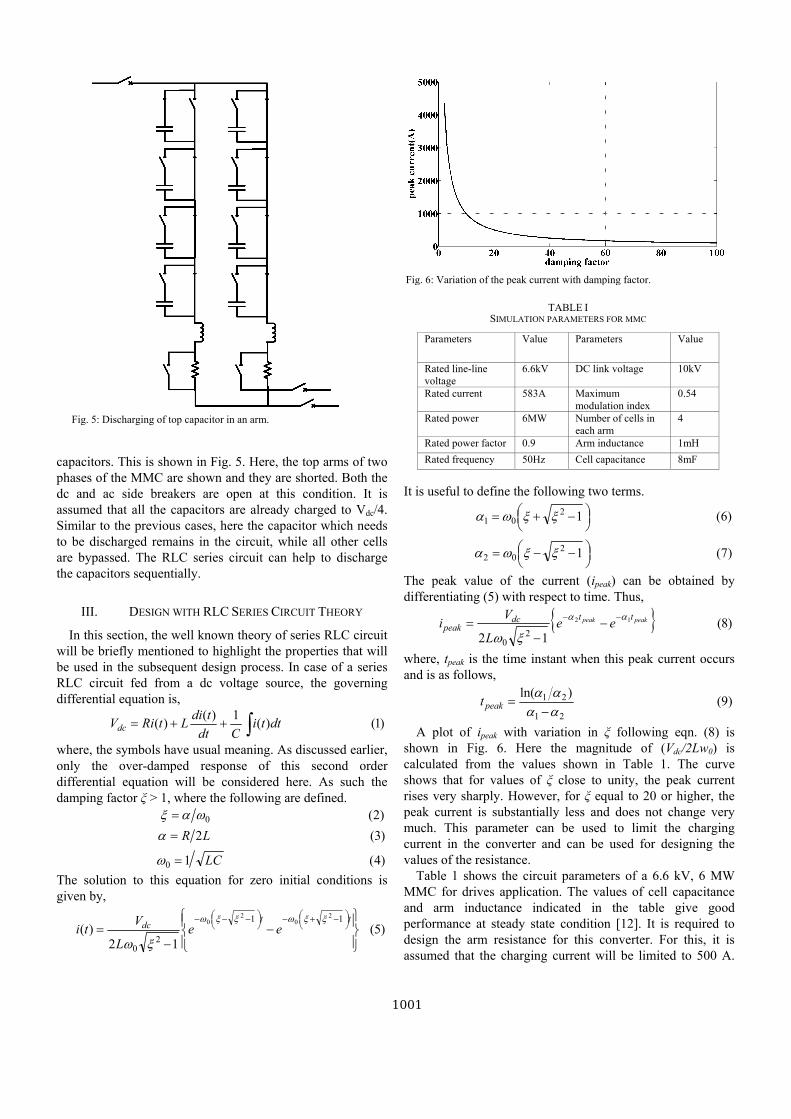
Fig. 5: Discharging of top capacitor in an arm.
Fig. 6: Variation of the peak current with damping factor.
capacitors. This is shown in Fig. 5. Here, the top arms of two phases of the MMC are shown and they are shorted. Both the dc and ac side breakers are open at this condition. It is assumed that all the capacitors are already charged to Vdc/4. Similar to the previous cases, here the capacitor which needs to be discharged remains in the circuit, while all other cells are bypassed. The RLC series circuit can help to discharge the capacitors sequentially.
III. DESIGN WITH RLC SERIES CIRCUIT THEORY
In this section, the well known theory of series RLC circuit will be briefly mentioned to highlight the properties that will be used in the subsequent design process. In case of a series RLC circuit fed from a dc voltage source, the governing differential equation is,
)1()(1)(
)( dttiCdt
tdiLtRiVdc
where, the symbols have usual meaning. As discussed earlier, only the over-damped response of this second order differential equation will be considered here. As such the damping factor ξ > 1, where the following are defined.
)2(0
)3(2LR
)4(10 LC
The solution to this equation for zero initial conditions is given by,
)5(12
)(11
20
20
20
tt
dc eeL
Vti
It is useful to define the following two terms.
)6(1201
)7(1202
The peak value of the current (ipeak) can be obtained by differentiating (5) with respect to time. Thus,
)8(12
12
20
peakpeak ttdcpeak ee
L
Vi
where, tpeak is the time instant when this peak current occurs and is as follows,
)9()ln(
21
21
peakt
A plot of ipeak with variation in ξ following eqn. (8) is shown in Fig. 6. Here the magnitude of (Vdc/2Lw0) is calculated from the values shown in Table 1. The curve shows that for values of ξ close to unity, the peak current rises very sharply. However, for ξ equal to 20 or higher, the peak current is substantially less and does not change very much. This parameter can be used to limit the charging current in the converter and can be used for designing the values of the resistance.
Table 1 shows the circuit parameters of a 6.6 kV, 6 MW MMC for drives application. The values of cell capacitance and arm inductance indicated in the table give good performance at steady state condition [12]. It is required to design the arm resistance for this converter. For this, it is assumed that the charging current will be limited to 500 A.
TABLE I SIMULATION PARAMETERS FOR MMC
Parameters Value Parameters Value
Rated line-line voltage
6.6kV DC link voltage 10kV
Rated current 583A Maximum modulation index
0.54
Rated power 6MW Number of cells in each arm
4
Rated power factor 0.9 Arm inductance 1mH
Rated frequency 50Hz Cell capacitance 8mF
1001
From Fig. 6, this will require a damping factor of 20. From eqns. (2), (3) and (4), the value of the arm resistance comes out be 10 ohms. During discharge of the cell as per Fig. 5, the peak discharge current is limited to Vdc/(8R) which is equal to 125 A and is an acceptable value.
IV. SIMULATION RESULTS
Some simulation results are shown in this section to validate the proposed concept.
In the first set, the circuit of Fig. 3 is followed where all the cells in the top arm are charged simultaneously. In Fig. 7, the dc side breaker is closed at t=0.1s. Since the dc bus is maintained at 10 kV, all the four capacitors are charged to 2.5 kV. The charging current during this time is shown in Fig. 8. The peak charging current is limited to 500 A, as expected from the design process. The current dies down to negligibly small values in less than a second.
The circuit of Fig. 4 is followed in case the cells are charged sequentially. Fig. 9 shows the charging process. At t=0.1s, the dc side breaker is closed and the top capacitor charges towards Vdc. Once the voltage on the top capacitor reaches 2.5 kV, it is disconnected and the second capacitor is inserted in the circuit. Subsequently all other capacitors in the arm are charged sequentially (Fig. 9). Once all the four capacitors in the top arm are charged, Si1 (i=1 to 4) are closed and the complementary switches opened. This will immediately bring the current in the circuit to zero (Fig. 10). The process is then followed for the bottom arm.
V. EXPERIMENTAL RESULTS
A small scale laboratory setup has been built for experimental validation of the proposed concept. As part of the process, each MMC cell is fabricated on a PCB, as shown in Fig. 11. The switches shown in Fig. 2 are realized using 100V, 10A MOSFETs (IRF520N). The gate drive circuit is also present on the board. It is only required to provide the gate pulses from the controller.
The parameters of the components used in the experimental setup have been listed in Table 2. Here, only 3 cells are inserted in each arm. All of them are simultaneously charged from a dc source of magnitude 75V. Based on eqn. (8) and the parameters from table 2, the charging current is limited to 1.7A.
One experimental result is shown in Fig. 12. The top three traces show the voltage build up in the three cells, while the bottom trace shows the charging current during this process. All the values obtained are as expected from the design process.
VI. CONCLUSION
In this paper, a method for charging and discharging the capacitors of an MMC has been discussed. The benefit of the charging circuit is that, it does not require any auxiliary voltage source. In case of drives application, the dc bus can be used to charge the capacitors easily. For this, an additional resistance is inserted in each arm of the MMC. This forms a series RLC circuit in each arm. By adjusting the resistance
Fig. 7: Simultaneous charging of 4 capacitors in an arm of MMC.
Fig. 8: Starting current variation during simultaneous charging of 4 cells in an arm of MMC.
Fig. 10: Starting current variation during sequential charging of 4 cells in an arm of MMC.
Fig. 9: Sequential charging of 4 capacitors in an arm of MMC.
1002

Fig. 11: Picture of one cell of the converter fabricated on a PCB.
Fig. 12: Charging process of 3 cells. Top three traces represent the charging process of the three capacitors in upper 3 cells. The bottom trace shows the charging current. Scales are embedded in the diagram.
value, as shown by the design process, the charging current can be controlled within acceptable values. Some simulation and experimental results are included to validate the concept.
ACKNOWLEDGMENT
The authors would like to thank Siemens Oil and Gas Divisions, Norway in providing financial support for this project.
REFERENCES
[1] A. Lesnicar and R. Marquardt, “An innovative modular multilevel converter topology suitable for a wide power range”, in Proc. of IEEE Power Tech Conf. 2003, pp. 1-6.
[2] M. Glinka and R. Marquardt, “A new AC/AC multilevel converter family,” IEEE Trans. Ind. Electron., Vol. 52, No. 3, June 2005, pp. 662-669.
[3] A. Lesnicar and R. Marquardt, “A new modular voltage source inverter topology,” in Proc. of EPE 2003, pp. 1-6.
[4] R. Marquardt, "Modular Multilevel Converter: An universal concept for HVDC-Networks and extended DC-Bus-applications", in Proc. of IPEC 2010, pp. 502-507.
[5] Antonopoulos, L. Angquist, and H.-P. Nee, “On dynamics and voltage control of the modular multilevel converter,” in Proc. of EPE 2009, pp. 1-10.
[6] S. Rohner, S. Bernet, M. Hiller and R. Sommer, "Modulation, Losses and Semiconductor Requirements of Modular Multilevel Converters", IEEE Trans. Ind. Electron., Vol. 57, No. 8, Aug. 2010, pp. 2633 – 2642.
[7] M. Hagiwara and H. Akagi, “Control and experiment of pulse-width modulated modular multilevel converters,” IEEE Trans. Power Electron, Vol. 24, No. 7, Jul 2009, pp. 1737-1746.
[8] Philipp Münch, Daniel Görges, Michal Izák and Steven Liu, "Integrated Current Control, Energy Control and Energy Balancing of Modular Multilevel Converters", in Proc. of IECON 2010, pp. 150-155.
[9] HVDC Plus- Siemens AG, available online at http://www.energy.siemens.com/hq/en/power-transmission/hvdc/hvdc-plus/
[10] Ke Li and Chengyong Zhao, "New Technologies of Modular Multilevel Converter for VSC-HVDC Application", in Proc. of APPEEC 2010, pp. 1-4.
[11] Jianzhong Xu, Chengyong Zhao, Baoshun Zhang and Li Lu, "New Precharge and Submodule Capacitor Voltage Balancing Topologies of Modular Multilevel Converter for VSC-HVDC Application", in Proc. of APPEEC 2011, pp. 1 – 4.
[12] A. Das, H. Nademi, and L. Norum, "A Pulse Width Modulation technique for reducing switching frequency for modular multilevel converter", in Proc. of IICPE 2010, pp. 1-6.
TABLE II EXPERIMENTAL PARAMETERS FOR MMC
Parameters Value Parameters Value
DC link voltage 75V Arm resistance 22 ohm
Arm inductance 1.5 mH Cell capacitance 6.8 mF Number of cells in
each arm 3
1003