a low-power, lightweight, wireless neural recording and … · a low-power, lightweight, wireless...
TRANSCRIPT
A Low-Power, Lightweight, Wireless Neural Recordingand Stimulating Headstage for Brain Machine Interfaces
Jaclyn Leverett
Electrical Engineering and Computer SciencesUniversity of California at Berkeley
Technical Report No. UCB/EECS-2014-206http://www.eecs.berkeley.edu/Pubs/TechRpts/2014/EECS-2014-206.html
December 1, 2014

Copyright © 2014, by the author(s).All rights reserved.
Permission to make digital or hard copies of all or part of this work forpersonal or classroom use is granted without fee provided that copies arenot made or distributed for profit or commercial advantage and thatcopies bear this notice and the full citation on the first page. To copyotherwise, to republish, to post on servers or to redistribute to lists,requires prior specific permission.
A Low-Power, Lightweight, Wireless Neural Recording andStimulating Headstage for Brain Machine Interfaces
by Jaclyn Leverett
Research Project
Submitted to the Department of Electrical Engineering and Computer Sciences, Universityof California at Berkeley, in partial satisfaction of the requirements for the degree of Masterof Science, Plan II.
Approval for the Report and Comprehensive Examination:
Committee:
Jan RabaeyResearch Advisor
Date
* * * * * *
Jose CarmenaSecond Reader
Date
1
Abstract
A Low-Power, Lightweight, Wireless Neural Recording and Stimulating Headstage forBrain Machine Interfaces
by
Jaclyn Leverett
Master of Science in Electrical Engineering and Computer Science
University of California, Berkeley
Professor Jan Rabaey, Chair
Brain Machine Interfaces have shown increasing promise to restore motor function topatients suffering from amputation or paralysis. However, for such systems to be clinicallyviable, both the implant and the external headstage must be wireless, ultra low power,compact, and inconspicuous. A lightweight, wireless headstage with a long battery life isalso necessary to perform meaningful experiments on small animals, such as rats and mice,while they are awake, untethered, and behaving naturally. The elimination of wires allowsfor a greater number of recording channels as well as interaction between multiple animalsin the same environment without the risk of tangling wires, a common problem that inhibitsproductivity as well as potentially harms the animals.
The focus of this work is on an external wireless neuromodulation system capable ofreal-time neural recording, on-chip data compression, and dual stimulation on 8 selectablechannels, hence offering substantially enhanced functionality over current state of the art(e.g. [7, 17, 3]). Weighing only 4.6 grams and dimensioned at 16mm x 29mm (the samearea as a quarter), this wireless headstage achieves a battery life of 10 hours when constantlytransmitting data at ranges up to 14 meters.
To achieve such a small form-factor with superior battery life, this headstage has in-tegrated ultra-low power components, including a 65nm CMOS 4.78mm2 neuromodulationApplication Specific Integrated Circuit (ASIC) that consumes 417uW from a 1.2V supplywhile operating 64 acquisition channels with epoch compression at an average firing rate of50Hz and engaging two stimulators with a pulse width of 250us/phase, differential currentof 150uA, and a pulse frequency of 100Hz.

i
Contents
Contents i
List of Figures iii
List of Tables v
1 Introduction 1
2 Fully-Integrated Neuromodulation System-On-Chip 42.1 Integrated System Level Overview . . . . . . . . . . . . . . . . . . . . . . . . 42.2 Neural Signal Acquisition . . . . . . . . . . . . . . . . . . . . . . . . . . . . 52.3 Digital Back-End . . . . . . . . . . . . . . . . . . . . . . . . . . . . . . . . . 62.4 Differential Stimulation . . . . . . . . . . . . . . . . . . . . . . . . . . . . . . 82.5 ASIC Summary and Comparison to State of the Art . . . . . . . . . . . . . . 9
3 First Steps: A Wired Neuromodulation System 113.1 Wired System Overview . . . . . . . . . . . . . . . . . . . . . . . . . . . . . 123.2 Wired 16ch Recording, 8ch Stimulating Headstage . . . . . . . . . . . . . . . 133.3 Wired System Base Station . . . . . . . . . . . . . . . . . . . . . . . . . . . 153.4 Wired System GUI . . . . . . . . . . . . . . . . . . . . . . . . . . . . . . . . 16
4 A Wireless Neuromodulation System 184.1 Wireless System Overview . . . . . . . . . . . . . . . . . . . . . . . . . . . . 184.2 Wireless Headstage Radio Considerations . . . . . . . . . . . . . . . . . . . . 214.3 Wireless Headstage Firmware . . . . . . . . . . . . . . . . . . . . . . . . . . 274.4 Wireless Headstage Power Regulation, Current Consumption, and Battery Life 36
5 Experimental Results 435.1 In Vivo Rat Testing . . . . . . . . . . . . . . . . . . . . . . . . . . . . . . . 435.2 Artificial Rat Testing . . . . . . . . . . . . . . . . . . . . . . . . . . . . . . . 46
6 Conclusion and Future Work 48

ii
Bibliography 50

iii
List of Figures
2.1 64 recording channels, 2 stimulators, digital compression and power conditioningare all integrated on a single 4.78mm2 IC. . . . . . . . . . . . . . . . . . . . . . 5
2.2 (Bottom) Block diagram of the signal acquisition chain. (Top) Performance sum-mary and noise spectral density. . . . . . . . . . . . . . . . . . . . . . . . . . . . 6
2.3 (Left) The digital block diagram. (Right) Power, data rate and compression ratiosunder the 3 different modes of operation. . . . . . . . . . . . . . . . . . . . . . . 7
2.4 Schematics for the differential stimulator and on-chip SC DC-DC. . . . . . . . . 82.5 Typical stimulation waveform recorded on benchtop depicting dynamic supply
switching and the measured stimulator current consumption over one cycle. . . . 92.6 System-on-chip summary and comparison to state of the art. . . . . . . . . . . . 10
3.1 Wired neuromodulation system that has allowed for the verification of our customintegrated system-on-chip (SoC) . . . . . . . . . . . . . . . . . . . . . . . . . . . 11
3.2 Three primary components of the wired system: The headstage, base station,and computer Graphical User Interface (GUI). . . . . . . . . . . . . . . . . . . . 13
3.3 (Top) Wired Headstage PCBs: AmpPCB (Left), which includes the amplifyingSoC, and IglooPCB (Right), which contains a low-power flash IGLOO AGL250V2FPGA. (Bottom) Mated PCBs form the headstage. . . . . . . . . . . . . . . . . 14
3.4 Circuit diagram of Low-Voltage Differential Signaling used to communicate be-tween the wired headstage and base station. . . . . . . . . . . . . . . . . . . . . 15
3.5 Highlevel diagram of the wired base station. . . . . . . . . . . . . . . . . . . . . 163.6 WibiGUI Spike Viewer showing epochs on one channel and Main Window dis-
playing real-time streamed neural data. . . . . . . . . . . . . . . . . . . . . . . . 17
4.1 High-level view of wireless neuromodulation system consisting of the headstage,base station, and computer Graphical User Interface. . . . . . . . . . . . . . . . 19
4.2 Close-up view of the wireless headstage, which measures 1.6cm x 2.9cm andweighs 4.6grams. . . . . . . . . . . . . . . . . . . . . . . . . . . . . . . . . . . . 20
4.3 Components of an auto-packetized nRF51822 radio packet. . . . . . . . . . . . . 234.4 The use of END/START shortcuts on the nRF51822 allows for the transmission
of multiple packets without disabling and re-enabling the radio. . . . . . . . . . 244.5 High level overview of ARM Cortex M0 firmware controlling the radio and ASIC. 28

iv
4.6 (Top) Traditional Serial Peripheral Interface (SPI) Mode 0 Communication. (Bot-tom) ASIC’s Communication Protocol. . . . . . . . . . . . . . . . . . . . . . . . 30
4.7 Solution: Using SPI Mode 0 allows for accurate latching of scan commands sentto the ASIC. . . . . . . . . . . . . . . . . . . . . . . . . . . . . . . . . . . . . . 31
4.8 Hardware connections used to achieve an SPI Slave Pseudo Master. . . . . . . . 334.9 Buck Converter Conversion Factors . . . . . . . . . . . . . . . . . . . . . . . . . 374.10 Discharge curve showing output voltage over time for a Lithium Polymer recharge-
able battery under various loads . . . . . . . . . . . . . . . . . . . . . . . . . . . 394.11 (Bottom)Power supply efficiencies of the 3.6V LDO and the nRF51822’s on-chip
Buck DC/DC converter over the range of Vbatt for a constant 15mA internalcurrent load. (Top) Estimated current pulled from the LiPo battery over itslifetime. . . . . . . . . . . . . . . . . . . . . . . . . . . . . . . . . . . . . . . . . 40
4.12 Base Station Block Diagram . . . . . . . . . . . . . . . . . . . . . . . . . . . . . 41
5.1 Raw streamed neural data (Top) and action potential epochs (Bottom) acquiredby our wired neuromodulation system . . . . . . . . . . . . . . . . . . . . . . . 44
5.2 Raw streams, epochs, and firing rates of in vivo recorded data. . . . . . . . . . . 455.3 In vivo stimulation artifact measured by neighboring amplifier channels. . . . . 465.4 Example “Artificial Rat” that feeds signals to a connector that mates with a
headstage. . . . . . . . . . . . . . . . . . . . . . . . . . . . . . . . . . . . . . . . 47

v
List of Tables
1.1 Comparison between this wireless neuromodulation headstage and other state-of-the-art systems. . . . . . . . . . . . . . . . . . . . . . . . . . . . . . . . . . . . . 3
4.1 Experimental effective data rates found for 64 and 128 Byte payloads. . . . . . . 254.2 Average Number of Unmatched CRCs over 10 tests of 10,000 received packets. . 254.3 Experimental transmission distances at which 0.1% of 10,000 received 64-Byte
data packets contained errors using a receiver with -85 dBm sensitivity and 0.1%BER . . . . . . . . . . . . . . . . . . . . . . . . . . . . . . . . . . . . . . . . . . 27
4.4 Breakdown of current required when transmitting 32 channels of action potentialepochs. Each channel is assumed to record neurons firing at an average rate of50 Hz. . . . . . . . . . . . . . . . . . . . . . . . . . . . . . . . . . . . . . . . . . 38

vi
Acknowledgments
There are truly so many people that have helped make this thesis possible. First, andforemost, I would like to thank my advisor, Professor Jan Rabaey, for his support andguidance throughout my graduate career. He has been an amazing mentor since I startedat Berkeley, making a significant effort to understand my interests and helping to shape mycareer plans. In addition, I would like to thank my other reader, Professor Jose Carmena,for his counsel during the design of this project.
Furthermore, this work would not have been possible without Dan Yeager, Will Bie-derman, and Nathan Narevsky, whose integrated circuit design enables an ultra-low powerwireless headstage and whose guidance and friendship I highly value. I would also like toexpress my gratitude toward Ryan Neely in Professor Carmena’s lab, whose work performinganimal surgeries and conducting in vivo experiments was truly invaluable.
Finally, I am so grateful for my husband, Zach Wasson, who has been an endless sourceof support during this great season of change in our lives, and for my mother, Carol, andmy father, Whit, for always encouraging me to pursue my dreams and to persist in the faceof adversity.

1
Chapter 1
Introduction
Brain Machine Interfaces have shown great potential to assist patients with neurological
damage, motor diseases, and limb amputation. The use of closed-loop stimulation in brain
machine interface research has become an area of increased interest in an effort to understand
the neuroplastic nature of the brain. For instance, electrical stimulation in response to neural
activity has been used as a more effective form of Deep Brain Stimulation for patients with
Parkinson’s Disease [4].
In addition to therapeutic applications, closed-loop BMI’s have the capability of revo-
lutionizing state-of-the-art prosthetic limbs. If an artificial limb has any hope of being a
suitable bio-replacement, a patient must be able to feel the location of the limb via proprio-
ception and receive sensory information about a grasped object. It has been shown in [14]
that sensory stimuli can be mimicked using cortical microstimulation, where rats integrated
stimulation sensations with their own knowledge of whisker orientation in order to identify
an artificial target. Making this type of neuromodulation clinically viable for humans, how-
ever, is dependent on the availability of a compact, wireless, battery-powered device that
can stimulate as well as record neural signals in real time.
Traditionally, neural signals have been recorded by wiring each implanted electrode to a
biopotential amplifier, and due to most recording systems’ power, weight, and size require-
ments, signal processing must be offloaded to a distant device, which necessitates a wired
tether to the test animal. This tether imposes physical and behavioral restrictions on the

CHAPTER 1. INTRODUCTION 2
animal, which must be either constrained to a small cage or anesthetized to prevent tangling
of wires and harming the animal. Furthermore, the movement of suspended cables as well
as the mechanical stress imparted on headstage connectors are significant sources of noise.
A commutator is often necessary to minimize tangling of wires, but since this is in the direct
signal path, it can also introduce undesirable noise. As greater numbers of neural recording
channels are desired, the required quantity of wires also increases, which does not scale well.
The use of a wireless system would enable not only more recording sites, but also more ex-
periments focused on social relationships between multiple free-roaming animals in the same
space.
Several wireless headstages have been designed in an attempt to solve the previously men-
tioned problems with varying levels of success. Across these wireless designs, it is universally
accepted that an optimal headstage should be: lightweight enough to sit on a small animal’s
head, small enough such that the animal does not notice the device, ultra-low power to pro-
vide maximum battery life for long experiments, and capable of communicating at distances
that allow for large cages to enable the animal to roam freely.
Compared to the state of the art listed in Table1.1, this headstage achieves the highest
level of integration, on-line programmability, and battery life with one of the lowest weights
and sizes. This wireless system also has the unique capability of three levels of digital
compression that can each be enabled on a per-channel basis, which allows for a greater
number of possible recording channels and a reduction in the required system power and
bandwidth. Additionally, the neuromodulation ASIC’s stimulation block enables spatiotem-
poral stimulation using two stimulators on eight available electrodes, and due to the high
voltage tolerance of the stimulators, the ASIC can drive LEDs for optogenetic stimulation
in addition to electrodes for electrical stimulation.
This thesis will first give an overview of the capabilities of the neuromodulation SoC
(designed by [16]) that make this wireless headstage possible. In the next chapter, we will
describe our custom wired neuromodulation system, which has allowed for the verification of
the custom integrated system-on-chip (SoC) and is critical to the testing and understanding
CHAPTER 1. INTRODUCTION 3
of the SoC’s abilities. The design of the wireless neuromodulation system will then be
thoroughly detailed, and finally, we will discuss in vivo as well as benchtop experimental
results.
This WorkBall et al.2014 [3]
TBSIW32-Series2014
Fanet al.2012 [7]
Szutset al.2011 [13]
Zhang et al.2012 [17]
NumberRecordingChannels
32 14 31 16 54 1
Number Stim-ulation Chan-nels
2 (8 Stim Sites) 0 0 0 0 3 (3 PresetStim Sites)
CompressionOptions
Action PotentialEpochs, FiringRates, Full DataStreaming
None None None None None
Per-ChannelOnline Con-figuration
Compressionlevels, chan-nel enabling,stimulation pa-rameters, gain,filter cutoffs
Gain, filtercutoffs, ref-erence selec-tion, inputgrounding
None None Gain,filteringcommonto allchannels
Stimulationparameters
Mass
4.6g includingseparate 8-chelectrical stimu-lation connector
22g 4.5g 4.5g 52g 10g
Battery Life 10hours 1.5hours 3.5 to4.2hours
6hours 6hours 1hour
Size 2.7cm3 4.3cm3 6.35cm3 2.2cm3 100cm3 3.7cm3
Range14m (0.1%transmissionlosses)
10m (0.1%transmis-sion losses)
4m 4m 60m 200m
Table 1.1: Comparison between this wireless neuromodulation headstage and other state-of-the-art systems.

4
Chapter 2
Fully-Integrated NeuromodulationSystem-On-Chip
Due to the complex nature of BMI systems, achieving low power, weight, and size would
not be feasible without custom integrated circuitry. Therefore, a highly integrated neu-
romodulation system-on-chip (SoC) was designed by [16] to operate 64 analog acquisition
channels, digitize and compress action potential data, and engage two stimulators on 8 se-
lectable channels without any off-chip components. Compared to the state of the art, this
substantially enhanced functionality system represents the lowest area and power for the
highest integration complexity achieved to date. The following paragraphs will discuss the
details of this SoC, which are key to making a wireless Brain Machine Interface possible.
2.1 Integrated System Level Overview
This 4.78mm2 SoC in 65nm CMOS consumes 417µW from a 1.2 Volt supply while oper-
ating 64 acquisition channels with epoch compression at an average firing rate of 50Hz and
engaging two stimulators with a pulse width of 250µs/phase, differential current of 150µA,
and a pulse frequency of 100Hz. This SoC is composed of 3 major functional blocks: Neural
Signal Acquisition, Differential Stimulation, and the Digital Back-End (Figure 2.1).

CHAPTER 2. FULLY-INTEGRATED NEUROMODULATION SYSTEM-ON-CHIP 5
Slide 1
ADC VGA LNA BPF
8x Amp Rows
BUF
CAC
8x
64 Recording Site
s
2x DifferenBal SBmulators
Power Train 1:7 DC-‐DC
Bias Gen, Ref & Regulators
8 Differen
Bal
SBmulaB
on Site
s
MUX 8x AMPLIFIERS
4x
Spike Detector
PackeBzer
Data Types
Raw Streams
Epochs
Firing Rates
Digital Back-‐End
Config Readout
FSM MUX
4x
MUX
Supply Sensor & Mux
Supply Sensor & Mux
SCAN
FIFO
+
-‐
Figure 2.1: 64 recording channels, 2 stimulators, digital compression and power conditioning areall integrated on a single 4.78mm2 IC.
2.2 Neural Signal Acquisition
In order to record action potentials that have low SNR, recording channels must provide
adequate noise performance while consuming minimal power and area. This SoC achieves
the lowest area per channel (0.0258mm2 with biasing and digitization) for an AC-coupled
design by 3x [10], allowing for integration with compression and stimulation in one integrated
circuit. The block diagram of the signal acquisition chain as well as the performance summary
and noise spectral density are detailed in (Figure 2.2). Every 8 amplifiers share an input
buffer (BUF) and digitizing circuits (ADC).
The SoC can accommodate up to 64 recording electrodes, and each group of 16 elec-
trodes shares 1 reference, which in practice is typically a nearby larger electrode with lower
input capacitance. Due to the differential LNA, large common mode signals such as those
from LFPs should be reduced. Several techniques were utilized to minimize overall power
consumption of the acquisition circuitry. Each VGA drives a separate sampling capacitor
to allow maximum settling time. A time-multiplexed SC amplifier (BUF) drives the 260fF
ADC input capacitance. To minimize power consumption of this buffer, the ADC sampling

CHAPTER 2. FULLY-INTEGRATED NEUROMODULATION SYSTEM-ON-CHIP 6
!"#$%&'()&*&+!)&*&,-.& /0&*&01/2&*&3/&4,&
56789%&'()&*&+!)&*&,-.& 3:/&*&;:<&*&3:0&=>&
'()%&?@(&*&(A.&*&5A.& 2:B&=+9CD&*&E:0&*&3/:F&)GH%&I,#JD&*&H6$K:&@"J8& 3;&L&*&30;&MDND&)GH%&G('&*&?('&*&A(O,& ;:P<&*&3:B&*&P:/&'Q,&
)GH%&56789&*&)98"& ;:/&=>&*&F/;;&=C/&
,#"D&!8$%&56789&*&)98"& /:3P&=>&*&;:;E&CC/&
HR"$$8S%&56789&*&)98"& 3:P<&=>&*&;:;/BP&CC/&
!"#$ %&#$'()*$$
+((,*$
'-.)*$
/0123/,*$ %45$
$67*$8((,*$ '((,*$
%45$
PT&
%45$
'(9$#:4$
?@(U2:B&=+9CD&$
,5.U;:B<1P:EMVW$
Figure 2.2: (Bottom) Block diagram of the signal acquisition chain. (Top) Performance summaryand noise spectral density.
window utilizes 22/32 of each conversion period, while successive approximation consumes
the remaining 10/32 cycles. The BUF requires 1.2µA to settle at 8*20kHz. Bottom plate
sampling is used in the ADCs. To avoid charge pumps and swings beyond the rails or a
power-hungry VDD/2 reference, half of the top plates are charged to VDD and the other
half are charged to GND during the sampling phase, effectively creating a VDD/2 refer-
ence. The split array has 6 binary and 4 thermometer bits to reduce DNL to less than 1bit.
Custom 260aF MOM unit capacitors allow for a compact low power ADC.
2.3 Digital Back-End
While high-density implantable recording systems are increasingly called for, the data rate
required is typically unsuitable for a data-rate constrained wireless link. In response to this
issue, programmable digital compression has been incorporated into this SoC, allowing for
customized data rate reduction on a per channel basis. Prior state-of-the-art multichannel

CHAPTER 2. FULLY-INTEGRATED NEUROMODULATION SYSTEM-ON-CHIP 7
neural signal compression implementations [2, 12, 6, 9] have not addressed the level of
integration and area-efficiency necessary for a long-term implantable system. A diagram
of the digital back-end (Figure 2.3) shows the entire interface to the block, with direct
connections to the ADCs and a 4-wire serial interface.
!"#$%&
'#&()&*+,&
-./01&+2134%&
-./01&(5634%&
7!8&9:;014&<=<,&
-;:3&&
(>5;0&?/%4"&
-4@1:$&&
+.5;)&&
9:;01AB1@&
</@/3C&D:41&
-;:3&+;)5&&
E?(&,FG&
?,FG&
H?EGE&
H-I-&
?=*&
'#&()&J/%45@K&L6M1@& !"#"$$%&'()$
&
'#&()&95N1@&'#&()&?:4:&D:41&
(5$.@1%%/53&D:A5&
D:N&-4@1:$&
!O8PQ&7O"'ROST.%&
7U&
+.5;)%&RVJBW()&
77O"'PQ&7"'O8#ST.%&
8"OU&
</@/3C&D:41%&
XX"'OPQ&!V0.T%&XVVU&
Figure 2.3: (Left) The digital block diagram. (Right) Power, data rate and compression ratiosunder the 3 different modes of operation.
A nonlinear energy operator [9] based spike detector extracts spike events, enabling data
reduction by only sending the 2.1ms spike window around an event (epochs), and/or spike
counts in a 2.4-50ms programmable window. Sending epochs, spike rates, and uncompressed
data (streams) can be enabled on a per channel basis. All packets are put into a clock
domain crossing FIFO, which allows the system clock to operate at a different frequency than
the output data rate, resulting in further power savings. (Figure 2.3) presents annotated
power consumption, data rates, and compression ratios with an average firing rate of 50
Hz on each channel. Firing rates, which are sufficient for BMI control [15], provide the
highest compression ratio of 700x. The 64 channel digital back-end occupies a total area
of 0.675mm2, a 2.95X reduction compared to previous state of the art [9] normalized to a
65nm technology, and is lower power than [2] which implements a simpler algorithm.

CHAPTER 2. FULLY-INTEGRATED NEUROMODULATION SYSTEM-ON-CHIP 8
2.4 Differential Stimulation
Two independent, differential, bi-phasic current stimulators can be adaptively multi-
plexed onto four electrode pairs for a total of 8 unique stimulation sites, allowing for spa-
tiotemporal stimulation patterns necessary for more realistic sensory input. Each stimulator
utilizes a single current source for both positive and negative stimulation phases, which miti-
gates the effects of current mismatch between phases and eliminates the need for calibration.
The stimulators have configurable pulse length and current amplitude of >500µA (differ-
ential) with a 7µA LSB. The INL and DNL were measured to be 0.082 and 0.039 LSB
respectively. The electrode pairs can also be used to drive LEDs for optogenetic stimulation.
The stimulator output common mode is set at mid-rail from a single fully-integrated
switched-capacitor DC-DC converter. The DC-DC is implemented using a Dickson ladder
topology with a maximum tunable input voltage of 1.3V and a conversion ratio of 1:7 as
shown in Figure 2.4. A maximum output voltage of 8.7V was measured and is limited by
the NWELL/PSUB breakdown voltage of the process.
VREF
High Voltage Detector φ1
φ1
φ2 φ2
Low Voltage Detector VHIGH
VLOW
cfg
VELEC
S>m#1 +Electrode S>m#1 –Electrode
MUX θ+ φ2
θ-‐
θ-‐ θ+ ctl
VHIG
H
6x 5x 4x 3x 2x
7x MUX
+
VLO
W
4x 3x 2x 1x
5x
0x
MUX
+
+
+
+ +
+
+
+
_
_
_
_
VIN
VIN
VIN
2xVIN
3xVIN
4xVIN
5xVIN
6xVIN
7xVIN
ϕ1
ϕ1 ϕ2 ϕ1 ϕ2 ϕ1 ϕ2
ϕ1
ϕ2
ϕ1
ϕ2
ϕ1
ϕ2
ϕ2
ϕ1
ϕ2
Figure 2.4: Schematics for the differential stimulator and on-chip SC DC-DC.

CHAPTER 2. FULLY-INTEGRATED NEUROMODULATION SYSTEM-ON-CHIP 9
The stimulator implements an adiabatic, charge-recycling architecture without off-chip
components, enabling a fully integrated system as opposed to state of the art [1]. A supply
sensor dynamically tracks the changing electrode voltage and selects one of 7 supply voltages
from the DC-DC in order to minimize power consumption over a stimulation cycle. A typical
stimulation pattern of 300µA differential current with 150µs per phase was performed on
bench-top with a 1kOhm/10nF RC electrode model; the measured electrode voltages and
stimulator supplies are shown in Figure 2.5. The measured input referred current supplied
by the DC-DC over one cycle of operation is also shown in Figure 2.5.
0 2 4 6
0
500
1000
Electrode Spread (V)
Stim
. Sup
ply
Cur
rent
(uA)
Pos. Phase
Neg. Phase
Elect. Current
Average
-‐300μA Diff.
Phase Transi=on
0 200 4000
2
4
6
8
Normalized Time (us)
Volta
ge (V
)
VHIGH +
VHIGH -‐
VLOW -‐
VLOW +
VELECT +
VELECT -‐
Pos. Phase Neg. Phase
Figure 2.5: Typical stimulation waveform recorded on benchtop depicting dynamic supply switch-ing and the measured stimulator current consumption over one cycle.
2.5 ASIC Summary and Comparison to State of the
Art
The final specifications of this SoC are summarized in Figure 2.6 and compared with
the state of the art. The SoC was tested in vivo using custom designed wired and wireless
systems. The rest of this thesis will focus on these systems that take advantage of the

CHAPTER 2. FULLY-INTEGRATED NEUROMODULATION SYSTEM-ON-CHIP 10
many beneficial features of this SoC and realize a compact, low-power, fully-integrated,
high-density wireless Brain Machine Interface.
System Specs. This Work [2] [10] [5]
Technology / VDD 65nm / 1.0V, 0.8V (Ana, Dig) 0.35um / 1.5V 180nm / 1.8V 0.35um / 5.0V
Off Chip Req? None 1uF Capacitor DC-‐DC 16-‐Ch. Recording IC
# Amp / SSm Ch. 64 / 8 8 / 8 4 / 8 16 (Off-‐Chip) / 8
Amp & ADC Power / Area per Ch.
1.81μW / 0.0258mm2 25.8 μW / 0.3122mm2
61.25μW / 0.354mm2
N/A
Gain / LP / HP
45-‐65dB / 10-‐1k / 3k-‐8k 51-‐65.6dB / 1-‐525Hz / 5-‐12kHz
54dB / 700hz / 6khz N/A
Noise / NEF/ PEF
7.5μVrms / 3.6 / 12.9 3.12μVrms / 2.9 (5.1kHz) / 12.6
Not Reported
N/A
SSm Imax / Area per Ch.
>500μA / 0.0675 mm2
94.5μA / 0.038mm2 4.2mA, 116μA / 0.05mm2
6.25mA / 0.7mm2
Compression or DSP Type
Raw Data, Epoch, Firing Rate (any combinaSon, per-‐ch.)
8 Spike Detector Outputs or 1 Ch. Raw
Log-‐DSP for LFP Energy, Output Mode: 4Ch Raw
Spike DetecSons, ClassificaSon, PCA
Digital Power / Area per Ch.
1.21μW (FR) & 1.775μW (Epoch) / 0.0105mm2
3.28μW / 0.0676mm2 34.5μW / 0.8mm2 256.875μW / 0.191mm2
*Area es(mated from die photo *
*
*
Figure 2.6: System-on-chip summary and comparison to state of the art.

11
Chapter 3
First Steps: A WiredNeuromodulation System
In this chapter, we present a wired neuromodulation system (Figure 3.1) that has allowed
for the verification of the custom integrated system-on-chip (SoC). This system was critical
to the testing and understanding of the SoC’s capabilities and thus will be described briefly
in the following paragraphs.
Figure 3.1: Wired neuromodulation system that has allowed for the verification of our customintegrated system-on-chip (SoC)

CHAPTER 3. FIRST STEPS: A WIRED NEUROMODULATION SYSTEM 12
3.1 Wired System Overview
The wired system is composed of three primary components: The headstage, base station,
and computer Graphical User Interface (GUI). The headstage contains our fully-integrated
neuromodulation System-on-Chip, an Omnetics neural nano-strip connector for 16 channels
of recording, an Omnetics neural nano-strip connector for 8 channels of differential stimu-
lation, an IGLOO AGL250V2 FPGA, and supporting circuitry. Information is transferred
between the headstage and the base station via a µHDMI cable. The base station serves as
an intermediary between the headstage and the computer’s GUI, which the user controls. A
diagram of this system is shown in Figure 3.2.

CHAPTER 3. FIRST STEPS: A WIRED NEUROMODULATION SYSTEM 13
!"#$
%&'$!()*&+,$-."/0,$
12)234$%&(*,$567!$$89:%9$
567!$$%9:89$
;<=$
%&($>2(0$=+.?&3(*@$A2/)"'2)*$B))&C$
!D+E?&D"3$#"++&3@,$
F&,*$!(&D"3$
G*&@,(&4*$HG7A=$#&I?*$
G*&@,(&4*$
Figure 3.2: Three primary components of the wired system: The headstage, base station, andcomputer Graphical User Interface (GUI).
3.2 Wired 16ch Recording, 8ch Stimulating
Headstage
The wired headstage is composed of two PCBs mated together through 1mm pitch 15-pin
headers. We will call the two boards IglooPCB and AmpPCB, shown in Figure 3.3. The
IglooPCB contains a low-power flash IGLOO AGL250V2 FPGA, which relays information to
the headstage from the Base Station and vice versa. The AmpPCB includes the amplifying

CHAPTER 3. FIRST STEPS: A WIRED NEUROMODULATION SYSTEM 14
SoC and supporting circuitry. Together, these PCBs form a small 16.5mm x 20.5mm x
5.5mm package. Even though the SoC can support up to 64 neural recording channels,
this headstage included connections for only 16 channels to be compatible with existing 16
channel implants in our partnered rat testing lab. However, the width of this headstage
was chosen such that the PCB could be easily adapted to include two-32 channel Omnetics
neural nano-strip connectors instead of a 16 channel connector once 32 channel implants for
rats were acquired.
The IGLOO FPGA was chosen for its size, low power requirements, versatile I/O power
supplies, and Low Voltage Differential Signaling capabilities. The AGL250V2 also has several
configurable I/O banks, making it ideal for communication between the SoC via 1.2V single-
ended I/O’s and the base station via LVDS drivers at 2.5V. The core of the AGL250V2 can
be set to as low as 1.2V, and it can consume as little as 5µW of power during Flash*Freeze
Mode. This IGLOO FPGA was programmed via JTAG using Microsemi’s Libero IDE.
Figure 3.3: (Top) Wired Headstage PCBs: AmpPCB (Left), which includes the amplifying SoC,and IglooPCB (Right), which contains a low-power flash IGLOO AGL250V2 FPGA. (Bottom)Mated PCBs form the headstage.

CHAPTER 3. FIRST STEPS: A WIRED NEUROMODULATION SYSTEM 15
LVDS Communication Through A µHDMI Cable
Communication between the headstage and base station is conducted using Low-Voltage
Differential Signaling (LVDS) through a µHDMI cable. LVDS is a high-speed, differential I/O
standard that requires a pair of I/O pins to carry one bit. External termination resistors are
also required. Figure 3.4 shows a full implementation of an LVDS transmitter and receiver,
including one resistor on the receiver end and three resistors on the transmitter end.
Figure 3.4: Circuit diagram of Low-Voltage Differential Signaling used to communicate betweenthe wired headstage and base station.
This I/O standard makes communication lines less susceptible to noise, particularly when
used with twisted pairs of wires. However, each LVDS pair consumes about 25mW of power
from a 2.5V supply, so it is only suitable for a wired system. A µHDMI cable was chosen
because it contains 4 twisted pairs, a power and ground line, and 3 single-ended lines.
This corresponds well to our SoC’s four main communication signals (DataOut, ScanIn,
SystemClock, and FifoClock) and reset signal.
3.3 Wired System Base Station
The wired base station is composed of four total PCBs: the Opal Kelly FPGA Integra-
tion Module, an IglooPCB, the RiserPCB, and the OKAdapter PCB. The IglooPCB mates
with the µHDMI cable, so it controls the LVDS drivers for communication with the wired
headstage’s IglooPCB. The IglooPCBs on the headstage and the base station are the same
design, just with slightly different LVDS resistor configurations, as explained in Section 3.2.
Figure 3.5 shows a block diagram of how the PCBs on the base station work together.

CHAPTER 3. FIRST STEPS: A WIRED NEUROMODULATION SYSTEM 16
RiserPCB!Opal Kelly XEM6310 FPGA
Module!
OKAdapter PCB!
Sends Scan Commands and Reset Signal to
IglooPCB
Receives Data Packets from IglooPCB
Receives Scan and Reset Commands
from GUI
Sends Data Packets to GUI
GUI
USB 3.0
Wired Base Sta2on
Provides Power to IglooPCB (3.3V)
IglooPCB!
Generates 20MHz Clock for IglooPCB
ScanIn
System Clock
FifoClock
DataOut
Reset
System Clock
DataOut
ScanIn
Reset
3.3V 3.3V Forwards Power to Headstage
(3.3V)
Converts Single Ended Signals to LVDS Signals
uHDMI!Cable!
(To Headstage IglooPCB)
Forwards Reset Signal to Headstage
Figure 3.5: Highlevel diagram of the wired base station.
The Base Station IglooPCB communicates with the Headstage IglooPCB via 4 LVDS
pairs and 1 single ended Reset signal, and it relays these signals to and from the Base
Station’s RiserPCB via a single-ended 3.3V I/O bank. The RiserPCB transmits signals
to/from the IglooPCB to the Base Station’s OKAdapterPCB, generates a 20MHz clock
signal to be used as the SoC’s SystemClock, and can supply 3.3V from a wall plug power
supply. The Base Station OKAdapterPCB was designed to allow the RiserPCB to interface
with two different Opal Kelly FPGA modules, the XEM6001 or the XEM6310. We have
chosen to use the XEM6310 for this application because it has more RAM to buffer our
incoming data stream, and it utilizes USB 3.0. The Opal Kelly XEM6310 sends and receives
signals from the OKAdapterPCB to the computer through its high speed USB 3.0 interface.
3.4 Wired System GUI
The Graphical User Interface (GUI) is the primary way the user interacts with the neu-
romodulation system. The GUI allows the user to select which channels of data he/she
CHAPTER 3. FIRST STEPS: A WIRED NEUROMODULATION SYSTEM 17
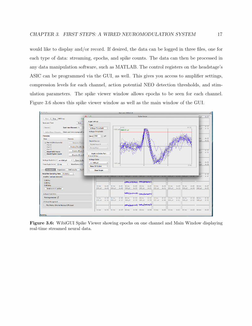
would like to display and/or record. If desired, the data can be logged in three files, one for
each type of data: streaming, epochs, and spike counts. The data can then be processed in
any data manipulation software, such as MATLAB. The control registers on the headstage’s
ASIC can be programmed via the GUI, as well. This gives you access to amplifier settings,
compression levels for each channel, action potential NEO detection thresholds, and stim-
ulation parameters. The spike viewer window allows epochs to be seen for each channel.
Figure 3.6 shows this spike viewer window as well as the main window of the GUI.
Figure 3.6: WibiGUI Spike Viewer showing epochs on one channel and Main Window displayingreal-time streamed neural data.

18
Chapter 4
A Wireless Neuromodulation System
In this chapter, we present a wireless, lightweight, low power, and compact head-mounted
neural modulation system. We will discuss design considerations, optimizations, and prin-
ciples of all the major components of this system, from the headstage itself to the wireless
base station and computer Graphical User Interface. By minimizing power and area, this
headstage serves as yet another important stepping stone on the way to restoring motor
function to patients suffering from amputation or paralysis.
4.1 Wireless System Overview
This wireless Brain Machine Interface system is composed of three main components: the
wireless headstage, the base station, and the Graphical User Interface (GUI) on a computer
(Figure 4.1).

CHAPTER 4. A WIRELESS NEUROMODULATION SYSTEM 19
!"#$
%&'$!()*&+,$-."/0,$
12)234$%&(*,$5")62/$%&62"7$8#9$
:9;$
%&($<2(0$;+.=&3(*6$82/)"'2)*$>))&?$
!@+A=&@"3$B$C)"4)&+$#"++&36,$
D&,*$!(&@"3$E*&6,(&4*$
5")62/$%&62"7$8#9$
F.&=$G*==?$1C:>$
HIJ:EK$<2)*=*,,$#"++I$
Figure 4.1: High-level view of wireless neuromodulation system consisting of the headstage, basestation, and computer Graphical User Interface.
The headstage forms a direct connection to a 32 channel microwire recording array that is
implanted within an animal’s cortex. At 1.6cm x 2.9cm, the area of this headstage (4.64cm2)
is equivalent to the area of a quarter (Figure 4.2), and it weighs 4.6grams. This headstage’s
size and weight was optimized for a mouse or rat, which can hold only 10% of their body
mass on their head; however, the headstage can easily be used on a monkey, and since the
headstages are so small, multiple could be used on a monkey to acquire recordings in several
different regions of the brain.

CHAPTER 4. A WIRELESS NEUROMODULATION SYSTEM 20
Figure 4.2: Close-up view of the wireless headstage, which measures 1.6cm x 2.9cm and weighs4.6grams.
The ASIC on the headstage digitizes and compresses action potential data, and the
headstage’s microcontroller/radio relays that information to the base station. The ASIC can
be programmed to acquire only certain channels, and the level of compression is selectable
on a per channel basis, so you can send raw streams of data, epoch spike windows, and/or
firing rates.
The base station forms a communication link between the headstage and the computer,
which displays data via a custom GUI. The GUI is used to visualize incoming neural data
on all 32 channels as well as send commands to the ASIC, such as channel and compression
selection and stimulation initiation.

CHAPTER 4. A WIRELESS NEUROMODULATION SYSTEM 21
4.2 Wireless Headstage Radio Considerations
4.2.1 Radio Selection
The two primary considerations for radio selection were power consumption and data
rate. Any combination of compression levels is possible; however, care should be taken to
select the combination that is within the data rate limits of the wireless headstage’s radio.
For a 32 channel system, if raw streaming, epochs, and firing rates were all enabled for
every channel where action potentials were firing at an average of 50 Hz, this would require
around 7.67 Mbps effective transmission data rate. Wifi could achieve this specification,
but unfortunately, it is at a very high power cost. For instance, TI’s CC3200 Wifi/MCU
System On-Chip can transmit at 9 Mbps, but it draws 225mA from a 3.6V supply [8]. With
our target size lithium ion battery (110mAh), that would equate to roughly 30 minutes of
battery life, which is unacceptable. Alternatively, Bluetooth Low Energy (BLE) would be
significantly lower power, but it suffers from poor data rates due to the significant protocol
overhead, radio limitations, and artificial software restrictions. Even though the modulation
rate of a BLE radio is 1Mbps, this theoretical maximum is never achieved. For instance, a
Nordic BLE SoC can transmit up to six 20 Byte packets of data per connection interval. If
the minimum connection interval dictated by the BLE specification is 7.5ms, this results in
a maximum effective data rate of 127kbps, which is much too low for our application.
The option with the most promise is a Nordic radio with a proprietary 2.4GHz protocol.
The modulation rate here is 2Mbps, and the required protocol overhead is significantly less
than that of Bluetooth Low Energy. However, because this is still a relatively low data
rate, it is pivotal to understand the compression levels of each of the 32 channels so we can
transmit data effectively.
Every channel of raw streamed data requires 213.3 kbps, regardless of the frequency of
action potentials, and firing rates require a constant data rate whether one or 32 channels
are selected. However, that data rate is dependent on a programmable firing rate window of
time. The window over which the number of spike events per channel is calculated can range

CHAPTER 4. A WIRELESS NEUROMODULATION SYSTEM 22
from 2.4ms to 50ms, and a 512bit data packet is sent after every window. Thus, the required
data rate for firing rates can range from 10.24 kbps to 213.33 kbps, but it is constant for
each selected time window.
Unlike the other levels of compression, the necessary epoch data rate is dependent on
frequency of neural activity. Every epoch data packet is 512 bits, so if one amplifying
channel detects action potentials fired by neurons at an average rate of 50 Hz, then 25.6
kbps is required per channel to send this data. For 32 channels, this is 819.2 kbps. Epoch
and firing rate level compression are highly recommended for the wireless headstage since
firing rates have been shown to be sufficient for Brain Machine Interface control algorithms
([5],[15]). Enabling raw streamed data is possible on the wireless headstage, but due to
the relatively large bandwidth required, it is most useful for initial setup and debugging
purposes.
The Nordic nRF51822 is particularly interesting since it is a system-on-chip with an
integrated ARM Cortex M0 32bit processor. The nRF51822 is a compact, low power solution
(3.5 x 3.8mm WL CSP) that requires 10.5mA peak TX at 0dBm at 2Mbps, 1Mbps, or
250kbps and 13.4mA peak RX at 2Mbps (-85 dBm sensitivity). Additionally, the use of
Serial Wire Debug (SWD) minimizes wires needed to program the microcontroller’s 256
kB embedded flash program memory. Direct Memory Access (DMA) is another extremely
valuable feature that allows a SPI block to write directly to memory, whose pointer can be
passed to the on-chip radio and transmitted seamlessly. The nRF51822 can also be powered
from supplies ranging from 1.8 to 3.6V. At supplies over 2V, the on-chip Buck converter
can be enabled to achieve further power savings during high current loads, such as when the
radio is on.
4.2.2 Effective Data Rates
The nRF51822’s automatic packet assembly and CRC generation/verification saves valu-
able CPU cycles, and with a packet payload of up to 255 bytes, the effective data rate can
be improved. For instance, using the 2Mbps data rate, due to some transmission bits needed

CHAPTER 4. A WIRELESS NEUROMODULATION SYSTEM 23
for a header and CRC footer as well as the time in between packets needed for the radio
to transmit the next packet, the 2Mbps is not the resultant data rate. If we can increase
the amount of data you send per packet, however, we can improve the ratio of data bits to
protocol bits. Each data packet received from the FIFO is 64 bytes long, so we could fit 3
full data packets in each transmission.
To find an estimate of the effective transmission data rate, the headstage was programmed
to constantly send radio payloads of either 64 bytes or 128 bytes, which corresponds to
sending 1 or 2 data packets.
The contents of the radio’s transmission packet can be seen in Figure 4.3. It consists of
a Preamble, Address, S0, Length, S1, Payload, and CRC. The preamble is always 1 Byte
while the address, payload, and CRC lengths are configurable. However, the sum of S0,
Length, S1, and Payload cannot exceed 255 Bytes (though S0, Length, and S1 can all be set
to 0 to achieve maximum payload length). To further improve data rate, the nRF51822’s
shortcuts can be used. A shortcut is a direct connection between an event and a task within
the same peripheral. If a shortcut is enabled, a specific task is automatically triggered when
its associated event is generated. Thus, we can use the END event generated after a data
packet is transmitted to trigger a radio START task, which will start transmitting the next
data packet. This significantly improves the effective data rate because the radio is able to
send multiple packets one after the other without having to disable and re-enable the radio
between packets (shown in Figure 4.4).
Figure 4.3: Components of an auto-packetized nRF51822 radio packet.
Theoretically, with the parameters used in our throughput test, the effective data rate
can be calculated as follows:

CHAPTER 4. A WIRELESS NEUROMODULATION SYSTEM 24
Figure 4.4: The use of END/START shortcuts on the nRF51822 allows for the transmission ofmultiple packets without disabling and re-enabling the radio.
Feffective = Ftrans ∗Bneural
Btotal
Where:
Feffective = Effective data rate
Ftrans = Frequency of Transmission (2Mbps)
Bneural = Neural Data Transmitted (64 Bytes)
Btotal = Total Bytes Transmitted ( Preamble [1 Byte] + Base Address [5 Bytes] + Payload
[1 to 255 Bytes] + CRC [2 Bytes] )
Using this equation, the effective data rate should be 1.78 Mbps using a 64 Byte payload
and 1.88 Mbps using a 128 Byte payload, which is similar to our experimental results detailed
in the following Table 4.1. In this experiment, we separated the wireless headstage from the
base station by 1 ft since we are just looking for an accurate estimate of the effective data
rate, barring the influence of transmission range.
To ensure that a significant percentage of transmitted packets were not being dropped due
to mismatched CRCs and therefore skewing effective data rates, the number of mismatched
CRCs in 10,000 incoming packets containing either a 64 or 128 Byte payload was counted.

CHAPTER 4. A WIRELESS NEUROMODULATION SYSTEM 25
Number of Packets ReceivedAverage Data Rate (Mbps)
64BytePayload 128BytePayload1,000 1.76 1.87500 1.77 1.88
Table 4.1: Experimental effective data rates found for 64 and 128 Byte payloads.
Based on observation of 10 of these tests, less than 10 packets with unmatched CRC’s were
identified per 10,000 radio packets (see Table 4.2).
Payload Size (Bytes) Average Number of Unmatched CRCs Percentage of CRCs Unmatched64 3 0.03%128 9 0.09%
Table 4.2: Average Number of Unmatched CRCs over 10 tests of 10,000 received packets.
4.2.3 Antenna Design
A variety of antenna options exist for 2.4GHz radios, so it was necessary to find the best
fit for our application. Size is a significant constraint in our wireless headstage because if the
device is too large, it may be not only too heavy for a small animal like a rat, but also too
noticeable to the animal, which may cause the animal to act unnaturally. In addition, the
range of wireless communication must not be too short since we want to allow for experiments
with larger cages that let the animals roam freely. Finally, we require an efficient antenna
to achieve our targeted range using as little power as possible.
The two main categories we explored were chip antennas and PCB antennas. A PCB
antenna is a cost-effective solution that is also low profile and lightweight since it is incor-
porated onto the PCB. However, the area required for a PCB antenna is typically quite
large. For instance, a quarterwave monopole 2.4GHz antenna would require a 23mm trace
(1.5mm wide trace on standard 1.6mm FR4) whereas the ceramic chip antenna we have
chosen for this application is only 6.5mm x 2.2mm. The use of meandering monopoles can
reduce PCB antenna area, but it is still larger than a ceramic chip antenna. Smaller chip
antennas than our chosen 6.5mm x 2.2mm component do exist, but as these get smaller,

CHAPTER 4. A WIRELESS NEUROMODULATION SYSTEM 26
the antenna gain is reduced, so this 6.5mm version represents a good compromise between
gain and area. Chip antennas can be smaller because they are made of a ceramic material
with a high dielectric constant. Furthermore, PCB trace antennas are more susceptible to
environmental effects, such as proximity to metal or batteries, housing material, and animal
contact, as well as ground plane size/shape because the PCB material typically has a low
dielectric constant (Ex: εr FR4 = 4). Chip antennas also tend to be more omni-directional
than PCB quarterwave monopoles. It is for these reasons that we proceeded with a ceramic
chip antenna.
4.2.4 Transmission Distances
The theoretical line of sight range of a link can be found using the Friis Transmission
Formula, which relates the free space path loss, antenna gains and wavelength to the received
and transmit powers of two antennas.
Pr
Pt
= GrGt ∗ (λ
4πR)2
Where:
Pr = Rx power of the wireless device receiving data
Pt = Tx power of the wireless device transmitting data
Gr = Rx antenna gain
Gt = TX antenna gain
λ = Wavelength of 2.4GHz wireless signal
R = Transmission distance in km
Using a Tx power of 0dBm and a Rx sensitivity of -85dBm at 2Mbps and assuming
antenna gains of 0.5dBi on each side, this yields a theoretical line of sight distance of about
86 meters. Of course, this is assuming ideal conditions and neglecting real-world variables
such as electronic noise, mismatched impedance, and interference from other 2.4GHz sources.
Experimental results have shown that our wireless headstage easily meets our 4-meter
target goal with 0dBm output power. However, extremely long ranges may not be necessary

CHAPTER 4. A WIRELESS NEUROMODULATION SYSTEM 27
in all applications. Therefore, if a shorter range is acceptable, we may reduce the headstage
radio’s output power to improve battery life at the cost of shorter transmission distances.
Table 4.3 shows the experimental transmission ranges found using various Tx output powers.
In this test, the wireless headstage was the transmitter, and the base station was the receiver.
Finding the ranges for this direction of communication is most relevant for a few reasons.
First, only the Tx powers of the nRF51822 can be adjusted, so Rx will always require the
same power. Second, the base station is not power constrained, so if necessary, it can operate
at the highest Tx output power. Finally, the communication link is heavily biased towards
the headstage transmitting and the base station receiving, so minimizing headstage Tx power
will greatly improve battery life.
At each TX output power, the range was determined to be the distance at which 0.1% of
10,000 64-Byte data packets contained errors, resulting in received packets with unmatched
CRCs. For this experiment, the headstage and base station PCBs were oriented parallel
to each other, which would correspond to the base station being attached to the top of a
cage/room with rats wearing headstages resting below.
Tx Power (dBm) Transmission Distance (m)+4 210 14-4 5.8-8 3.9-12 3
Table 4.3: Experimental transmission distances at which 0.1% of 10,000 received 64-Byte datapackets contained errors using a receiver with -85 dBm sensitivity and 0.1% BER
4.3 Wireless Headstage Firmware
4.3.1 High Level Overview
The ARM Cortex M0 processor on the nRF51822 serves as an intermediary between the
2.4GHz radio and the ASIC. A high level overview of the firmware controlling the wireless

CHAPTER 4. A WIRELESS NEUROMODULATION SYSTEM 28
headstage system is displayed in Figure 4.5 and contains two main components: The Radio
and SPI blocks. The Radio receives Scan commands from the base station and writes them to
the ScanIn Fifo. The Serial Peripheral Interface (SPI) block of the nRF51822 then transmits
the commands to the ASIC. Once the ASIC has a valid data packet to send back to the
microcontroller, the SPI block writes the packet into the DataOut Fifo, where the Radio
reads and transmits it to the base station.
Neuro-Modulation!
ASIC!DataOut Fifo!
ScanIn Fifo!Enable Ch.1 & Ch.2 Epochs!
Enable Ch.16 Firing Rates!
Enable Ch.2 Streaming!
2.4GHz Radio!
Success: Ch.1-2 Epochs Enabled!
Ch.1!
Ch.2!
SPI Block!(Serial Peripheral
Interface)!
nRF51822 SoC!
write!
write!
read!
read!
!"#"$%"&'(#)*'+,--)*.&'/0,-'1)&"'(2)3,*'
("*.&'4)2)'5)#6"2&'2,'1)&"'
(2)3,*'
("*.&'(#)*'+,--)*.&'2,'
7(8+'
!"#"$%"&'4)2)'5)#6"2&'/0,-'7(8+'
Figure 4.5: High level overview of ARM Cortex M0 firmware controlling the radio and ASIC.
4.3.2 ASIC Communication Intricacies
Interfacing off-the-shelf components with custom integrated circuits, such as this ASIC,
is challenging and often requires clever communication strategies, which will be detailed in
the following paragraphs.

CHAPTER 4. A WIRELESS NEUROMODULATION SYSTEM 29
4.3.3 Resetting and Aligning the ASIC
The ASIC uses 4 wires for communication: FifoClock, DataOut, ScanIn, and Reset.
There is also a SystemClock line, where the microcontroller could provide a system clock to
the ASIC, but simply enabling the ASIC’s on-chip crystal oscillator supplies the ASIC with
its own 20MHz clock, reducing the microcontroller’s CPU overhead.
Reset is an asynchronous, active-high signal, which resets the ASIC to its initial state.
Since there is no flash memory on the ASIC, all configuration parameters are cleared upon
reset, and the 20MHz crystal oscillator providing the system clock is disabled. Before any
instructions can be relayed to the ASIC, the FifoClock line must send 511 rising edges. This
is due to a minor initialization bug on the ASIC, but after these 511 bits have been clocked
out, normal 512 bit data packets can be removed from the ASIC without difficulty.
4.3.4 Serial Communication
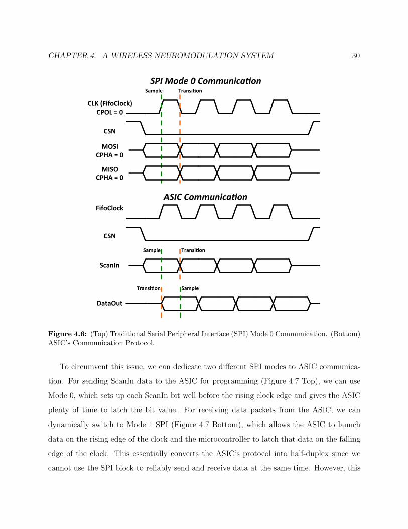
The ASIC implements a synchronous serial communication protocol that is not standard.
The ARM Cortex M0 on the nRF51822 has dedicated SPI and I2C blocks, so to efficiently
transfer data, is it wise to take advantage of this hardware. While the ASIC’s communication
is not standard, it is most similar to SPI. However, while SPI has two data lines whose data
are in phase with one another, the ASIC’s two data lines are offset from one another. An
example of traditional SPI Mode 0 communication is shown in Figure 4.6 on the top, and
the ASIC’s communication protocol is shown in on the bottom.
SPI is a full-duplex protocol, meaning that for every active clock edge, one bit of data is
sent and one bit of data is received. The ASIC’s communication protocol is also full-duplex,
but its scan and data lines do not have the same phase. For that reason, if we were to use the
SPI Mode 0 protocol to send and receive data, we would run into timing issues. For example,
on every rising edge of FifoClock on the ASIC, a ScanIn bit is latched and a DataOut bit is
transitioned. If the microcontroller tried to latch this DataOut bit on the rising FifoClock
edge, then it would be latching a transitioning value.
CHAPTER 4. A WIRELESS NEUROMODULATION SYSTEM 30
CLK (FifoClock) CPOL = 0
CSN
MOSI CPHA = 0
Sample Transi@on
FifoClock
CSN
ScanIn
Sample Transi@on
DataOut
Transi@on Sample
ASIC Communica-on
SPI Mode 0 Communica-on
MISO CPHA = 0
Figure 4.6: (Top) Traditional Serial Peripheral Interface (SPI) Mode 0 Communication. (Bottom)ASIC’s Communication Protocol.
To circumvent this issue, we can dedicate two different SPI modes to ASIC communica-
tion. For sending ScanIn data to the ASIC for programming (Figure 4.7 Top), we can use
Mode 0, which sets up each ScanIn bit well before the rising clock edge and gives the ASIC
plenty of time to latch the bit value. For receiving data packets from the ASIC, we can
dynamically switch to Mode 1 SPI (Figure 4.7 Bottom), which allows the ASIC to launch
data on the rising edge of the clock and the microcontroller to latch that data on the falling
edge of the clock. This essentially converts the ASIC’s protocol into half-duplex since we
cannot use the SPI block to reliably send and receive data at the same time. However, this
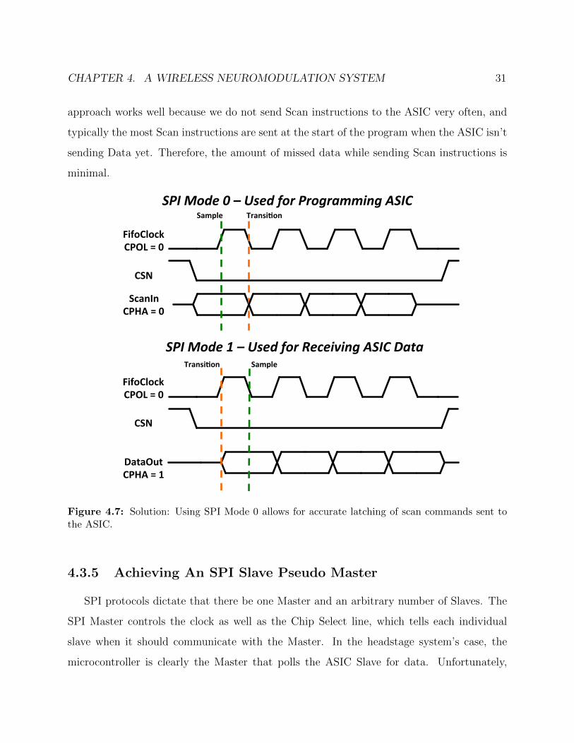
CHAPTER 4. A WIRELESS NEUROMODULATION SYSTEM 31
approach works well because we do not send Scan instructions to the ASIC very often, and
typically the most Scan instructions are sent at the start of the program when the ASIC isn’t
sending Data yet. Therefore, the amount of missed data while sending Scan instructions is
minimal.
FifoClock CPOL = 0
CSN
ScanIn CPHA = 0
Sample Transi<on SPI Mode 0 – Used for Programming ASIC
FifoClock CPOL = 0
CSN
SPI Mode 1 – Used for Receiving ASIC Data
DataOut CPHA = 1
Transi<on Sample
Figure 4.7: Solution: Using SPI Mode 0 allows for accurate latching of scan commands sent tothe ASIC.
4.3.5 Achieving An SPI Slave Pseudo Master
SPI protocols dictate that there be one Master and an arbitrary number of Slaves. The
SPI Master controls the clock as well as the Chip Select line, which tells each individual
slave when it should communicate with the Master. In the headstage system’s case, the
microcontroller is clearly the Master that polls the ASIC Slave for data. Unfortunately,

CHAPTER 4. A WIRELESS NEUROMODULATION SYSTEM 32
while there are Master and Slave dedicated hardware blocks on the microcontroller, only
the Slave is granted Direct Memory Access (DMA), which is absolutely essential for our
application. DMA allows the SPI Slave block to receive data and write it directly to a
memory address. For instance, we know the ASIC sends data packets in 512 bit blocks,
so the microcontroller’s CPU simply needs to kick off the SPI transfer, after which it can
go to sleep. Once all 512 bits have been written to memory, a flag is set and an interrupt
is triggered. A pointer to this block of data can then be handed over to the radio, which
seamlessly transmits the block.
In comparison, when the SPI Master receives data, it can only fill a 1 Byte buffer each
time. Once the 1 Byte has been filled, it sets a flag that the CPU must acknowledge and
clear before acquiring the next Byte. The CPU is also responsible for copying this Byte to a
dedicated memory address. Since we must acquire data in 512 bit packets, this corresponds
to 64 interrupts called, 64 bytes copied, and 64 flags cleared. While the SPI Master can use
a faster clock of up to 8 MHz versus the Slave’s maximum clock of 2 MHz, the Master still
requires greater CPU overhead.
Now that we have made the case for using the SPI Slave block, we will explain how
this can be achieved. As mentioned previously, the Slave requires an input clock and a
Chip Select signal to trigger the acquisition of data. The clock can be generated using two
timers in addition to the nRF51822’s convenient timer shortcuts, Programmable Peripheral
Interconnect (PPI), and GPIO Task Event blocks (GPIOTE). Because a GPIO cannot be
assigned to both the GPIOTE and SPI Slave blocks, two pins are required and must be
shorted together. This SPI clock is generated on SPISClockOutput (assigned to the GPIOTE
block) and received as an input on SPISClockInput (assigned to the SPI Slave block). Each
SPI transmission consists of 512 x 2MHz clock cycles as well as an active-low Chip Select line
(CSN). Since we are using the SPI Slave block, we must generate our own CSN by tying two
pins together. The hardware connections necessary for this communication trick are drawn
in Figure 4.8.

CHAPTER 4. A WIRELESS NEUROMODULATION SYSTEM 33
FifoClock
ScanIn
DataOut
SCLK
CSN
MISO
MOSI
Generated 2MHz Clock
Generated CSN Neuromodula*on ASIC Communica*on
Pins SPI Slave Block Pins
SPI Slave Pseudo Master
Figure 4.8: Hardware connections used to achieve an SPI Slave Pseudo Master.
4.3.6 Programming the ASIC
The ASIC can be programmed using Scan chain commands. Each command is 100 bits
long, with a 20 bit header and an 80 bit payload. Due to the fact that with every rising
clock edge the ASIC sees, it sends out one bit of a 512 bit data packet on the DataOut line,
we must take care to keep the packets aligned.
Thus, regardless of whether a command is being sent or not, every SPI transaction must
be in multiples of 512 bits. For instance, a 100 bit scan command can be sent to the ASIC,
but it must be followed by 412 zeros. Even though multiple scan commands could fit within
one 512 bit packet, only one command should be sent at a time. This is due to a complication
involving crossing of the two clock domains, one controlling the Fifo frequency and the other
at the system clock frequency of 20 MHz. Once a scan command has been received, the ASIC
generates and places in the Fifo an associated Config packet that echoes the scan command.
This serves as a verification that the ASIC has successfully received the command. Once the
Config packet has been placed in the Fifo, a flag is cleared. This flag can only be cleared
within a 2.4ms time window. If the flag is not cleared, the same Config packet will be placed
in the Fifo indefinitely, which can only be stopped with a system reset.

CHAPTER 4. A WIRELESS NEUROMODULATION SYSTEM 34
To overcome this issue, we must toggle the FifoClock line until we have received the
Config packet on the DataOut line. This is achieved by sending multiple scan commands
containing 512bits of zeros, so it takes effectively 3ms to commit a scan command and receive
a config packet safely. The need to send extra clock edges to clear the Fifo flag is inefficient;
however, the primary time that we will send a large number of scan commands is when the
ASIC has been reset. If we assume that there are 70 scan commands to be sent (One digital
and one analog command for each of the 32 channels, one analog command for each of the
4 amplifier rows, one global analog command, and one global digital command), then even
with this added delay, we should be able to program the ASIC in about 0.2 seconds, which
is a reasonable start up sequence. After this initialization, scan commands can be sent over
the air via the computer’s GUI, where only one command needs to be sent at a time.
4.3.6.1 Headstage Modes of Operation
Due to the fact that the Nordic 2.4GHz radios are half-duplex, meaning data can be sent
through only one direction of the link at a time, a strategy must be developed to efficiently
communicate given various goals. Because the wireless headstage typically has more data to
transmit than to receive, we can set the headstage as the wireless link Master. The Master
will spend the majority of its time transmitting neural data packets to the base station
(Slave) and will periodically check to see if the base station has anything it would like to
transmit. The period of this cycle is determined by the mode of the system, which can be
selected from the following: Programming Mode, Data Streaming Mode, and Stimulation
Mode. The base station sets which mode the system should be in since mode selection comes
from the computer’s GUI.
4.3.6.1.1 Programming Mode Programming Mode is the default state of the head-
stage once it has been turned on. During this mode, the base station sends a 512 bit packet
containing one scan command, which is received by the headstage and sent to the ASIC.
The ASIC returns a config packet, which needs to be returned to the base station so that the

CHAPTER 4. A WIRELESS NEUROMODULATION SYSTEM 35
base station acknowledges a successful programming command. The headstage will trans-
mit 1 packet before sending another polling packet to the base station. If the base station
successfully receives a Config packet, it can send a response packet indicating whether the
headstage should remain in Programming Mode or switch to another state.
4.3.6.1.2 Data Streaming Mode During Data Streaming Mode, the emphasis of band-
width is on transmitting neural data from the headstage to the base station. Therefore, the
headstage is set to transmit 1800 packets of data and then send a polling packet to ask the
base station if it should continue in Data Streaming Mode or switch to another state. The
headstage waits for a response from the Base Station, but if a time-out is met and a re-
sponse packet has not been received, then the headstage continues in Data Streaming Mode.
1800 packets was chosen to try to maximize neural data transfer while minimizing latency
between when the user sends a scan command and when the command actually reaches the
ASIC. If our experimental effective data rate when transmitting 128 Bytes of neural data
from the headstage was 1.87 Mbps, if we stop transmitting every 1800 packets, wait for a
polling packet (taking 0.54ms or meeting a 1ms timeout), and continue transmitting neural
data, then our effective data rate becomes 1.866 Mbps. Furthermore, sending 1800 packets
would take about 0.5 seconds, which is an acceptable worst case latency for sending a scan
command.
4.3.6.1.3 Stimulation Mode This wireless headstage is capable of not only recording
32 channels of neural data, but also driving two independent, differential, bi-phasic current
stimulators that can each be multiplexed onto four electrode pairs for a total of 8 unique
stimulation sites. Stimulation is achieved using scan commands, which can adjust the pulse
length and the current amplitude to greater than 500µA (differential) with a 7µA LSB. The
electrode pairs can also be used to drive LEDs for optogenetic stimulation.
The operator of the GUI can choose whether to send Stimulation Commands during Data
Streaming or Stimulation Mode. The primary difference between the two is that Stimulation

CHAPTER 4. A WIRELESS NEUROMODULATION SYSTEM 36
Mode allows the headstage to transmit only 200 neural data packets before it can receive a
stimulation scan command. If only one stimulation command needs to be sent every minute,
then there is no need to switch to Stimulation Mode. However, if the operator expects to
send many stimulation commands one after the other, he/she should enter Stimulation Mode
to minimize the latency from when the researcher tells the GUI to stimulate to when the
stimulation command is send to the ASIC, which would be a maximum of 55ms.
4.4 Wireless Headstage Power Regulation, Current
Consumption, and Battery Life
In order to be clinically viable, the battery life of wireless brain machine interfaces must
be as long as possible. The need to replace batteries throughout the day is cumbersome and
prevents patients from living full lives. In the realm of neuroscience, battery life of wireless
headstages should be long enough to conduct significant experiments without replacing bat-
teries and, consequently, losing data. Current state-of-the-art wireless headstages suitable
for small rodents have a battery life of only 4 hours ([7]). We have targeted a goal of 10
hours of battery life while constantly transmitting neural data packets. Ultra-low power
component selection is key to achieving our targeted battery life, and the ASIC is essential
to this application because it has been optimized for low power amplification, digitization,
and stimulation.
Furthermore, a Buck DC/DC converter was used to efficiently lower the Lithium ion bat-
tery’s 3.7V nominal voltage down to a usable range for the nRF51822. This Buck converter
can be enabled or disabled on the nRF51822, so it is important to know when it should be
used. The Buck converter is most efficient when it is supplying large currents and when it is
dropping down a high supply voltage. The figure below helps to make the decision of when
to enable the Buck converter.
The current supplied by the Buck converter is calculated using the following equation:
IDD,DC/DC = FDC/DC ∗ IDD

CHAPTER 4. A WIRELESS NEUROMODULATION SYSTEM 37
Where:
IDD,DC/DC = Current drawn from the external power supply when the DC/DC is enabled
FDC/DC = Current conversion factor based on DC/DC converter efficiency found in
Figure 4.9
IDD = Internal current drawn from the device power regulators
If FDC/DC < 1, then IDD,DC/DC < IDD, resulting in a decrease in power consumption.
However, if FDC/DC > 1, then IDD < IDD,DC/DC , which results in an increase in power
consumption. This is due to the base run current of the DC/DC converter being the dominant
factor.
Figure 4.9: Buck Converter Conversion Factors
The mode of operation in which the headstage is likely to spend the most time is the Data

CHAPTER 4. A WIRELESS NEUROMODULATION SYSTEM 38
Streaming Mode, where the headstage is, for the most part, constantly transmitting data
packets to the base station. Therefore, we will use this mode to determine the battery life
of the headstage. Since this system is better suited for sending primarily epochs and action
potential counts, we will enable both of these data types for all 32 channels. However, because
the data rate required to send epochs is dependent on the firing rate of each channel, we will
assume an average firing rate of 50 Hz per channel. In this situation, the ASIC consumes
approximately 114.7µW, which is negligible in comparison to the radio’s power consumption.
If transmitting at 0dBm, the radio consumes 10.5mA, and the 16MHz clock requires 470µA.
The running current consumption of the Cortex M0 processor is 275µA/MHz, which equates
to 4.4mA at 16MHz. Without the buck converted enabled, the entire system consumes about
15mA while constantly transmmitting, and when the buck converter is enabled, the amount
of current pulled from the battery drops to about 11mA.
Component Typical Current RequiredASIC 114.7µW
nRF51822 Radio 10.5mAnRF51822 ARM Cortex M0 4.4mA
Power Reg Quiescent Current 50µ[email protected] + [email protected]
Table 4.4: Breakdown of current required when transmitting 32 channels of action potentialepochs. Each channel is assumed to record neurons firing at an average rate of 50 Hz.
4.4.1 Lithium Polymer Battery
A 110mAh Lithium Polymer rechargeable battery was chosen for the wireless headstage
due to its size, capacity, peak current, and operating voltage. Since the PCB and attached
electronics weigh only 1.6 grams, the battery dominates the headstage weight with a mass of
3 grams. At 5.7 x 12 x 28mm, the battery is approximately the same size as the PCB of the
headstage. Since there are a wide variety of Lithium Polymer batteries in different charge
capacities, the user can optimize the headstage for either weight or battery life. The 110mAh
battery chosen was a compromise between weight and charge capacity. However, if testing on
larger animals that can accommodate heavier headestages, then a 150mAh Lithium Polymer

CHAPTER 4. A WIRELESS NEUROMODULATION SYSTEM 39
battery weighing 4.65 grams at 3.8 x 19.75 x 26.02mm or a 400mAh Lithium Polymer battery
weighing 9 grams at 5 x 25 x 35mm can be used.
The operating characteristics of Lithium Polymer batteries were well suited to our ap-
plication, as well. Based on preliminary calculations, we estimated that our system would
require about 15mA of current, which can easily be supplied by our 110mAh Lithium Poly-
mer battery, which has a 2C peak current (220mA). The voltage of Lithium Polymer cells
is a nominal 3.7V, which is around the nRF51822’s recommended operating voltage range
of 1.8 to 3.6V. The nRF51822 is rated to 3.9V, and since the output voltage of a Lithium
Polymer battery can begin at up to 4.2V, a Low Drop-Out regulator (LDO) is used to drop
the supply voltage to a constant 3.6V to prevent damaging the nRF51822. The voltage
curve of a typical Lithium Polymer battery is shown in Figure 4.10 [11]. The majority of
the battery’s lifetime is spent around 3.7V, giving the LDO high efficiency.
Figure 4.10: Discharge curve showing output voltage over time for a Lithium Polymer rechargeablebattery under various loads
The efficiency of a LDO is given in the following equation:
%LDO Efficiency =Iout ∗ Vout
(Iout + Iquiescent) ∗ Vbatt
∗ 100
CHAPTER 4. A WIRELESS NEUROMODULATION SYSTEM 40
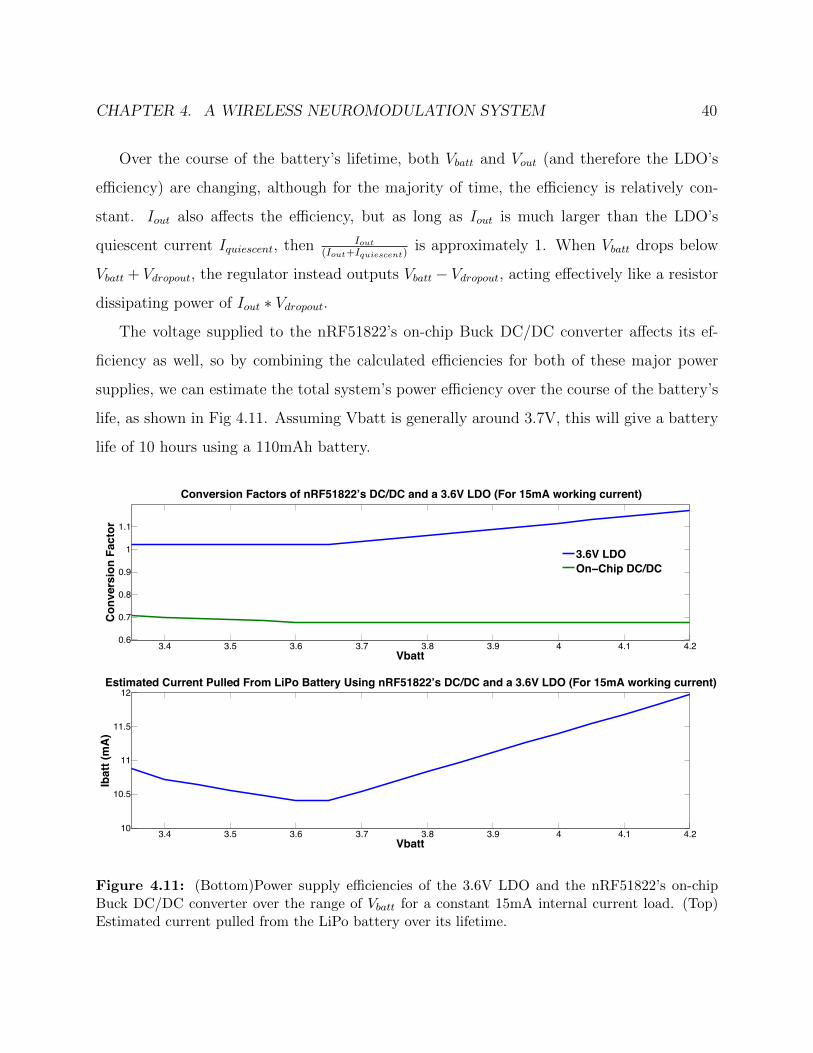
Over the course of the battery’s lifetime, both Vbatt and Vout (and therefore the LDO’s
efficiency) are changing, although for the majority of time, the efficiency is relatively con-
stant. Iout also affects the efficiency, but as long as Iout is much larger than the LDO’s
quiescent current Iquiescent, then Iout(Iout+Iquiescent)
is approximately 1. When Vbatt drops below
Vbatt + Vdropout, the regulator instead outputs Vbatt − Vdropout, acting effectively like a resistor
dissipating power of Iout ∗ Vdropout.
The voltage supplied to the nRF51822’s on-chip Buck DC/DC converter affects its ef-
ficiency as well, so by combining the calculated efficiencies for both of these major power
supplies, we can estimate the total system’s power efficiency over the course of the battery’s
life, as shown in Fig 4.11. Assuming Vbatt is generally around 3.7V, this will give a battery
life of 10 hours using a 110mAh battery.
3.4 3.5 3.6 3.7 3.8 3.9 4 4.1 4.210
10.5
11
11.5
12
Vbatt
Ibat
t (m
A)
Estimated Current Pulled From LiPo Battery Using nRF51822’s DC/DC and a 3.6V LDO (For 15mA working current)
3.4 3.5 3.6 3.7 3.8 3.9 4 4.1 4.20.6
0.7
0.8
0.9
1
1.1
Vbatt
Con
vers
ion
Fact
or
Conversion Factors of nRF51822’s DC/DC and a 3.6V LDO (For 15mA working current)
3.6V LDOOn−Chip DC/DC
Figure 4.11: (Bottom)Power supply efficiencies of the 3.6V LDO and the nRF51822’s on-chipBuck DC/DC converter over the range of Vbatt for a constant 15mA internal current load. (Top)Estimated current pulled from the LiPo battery over its lifetime.
CHAPTER 4. A WIRELESS NEUROMODULATION SYSTEM 41
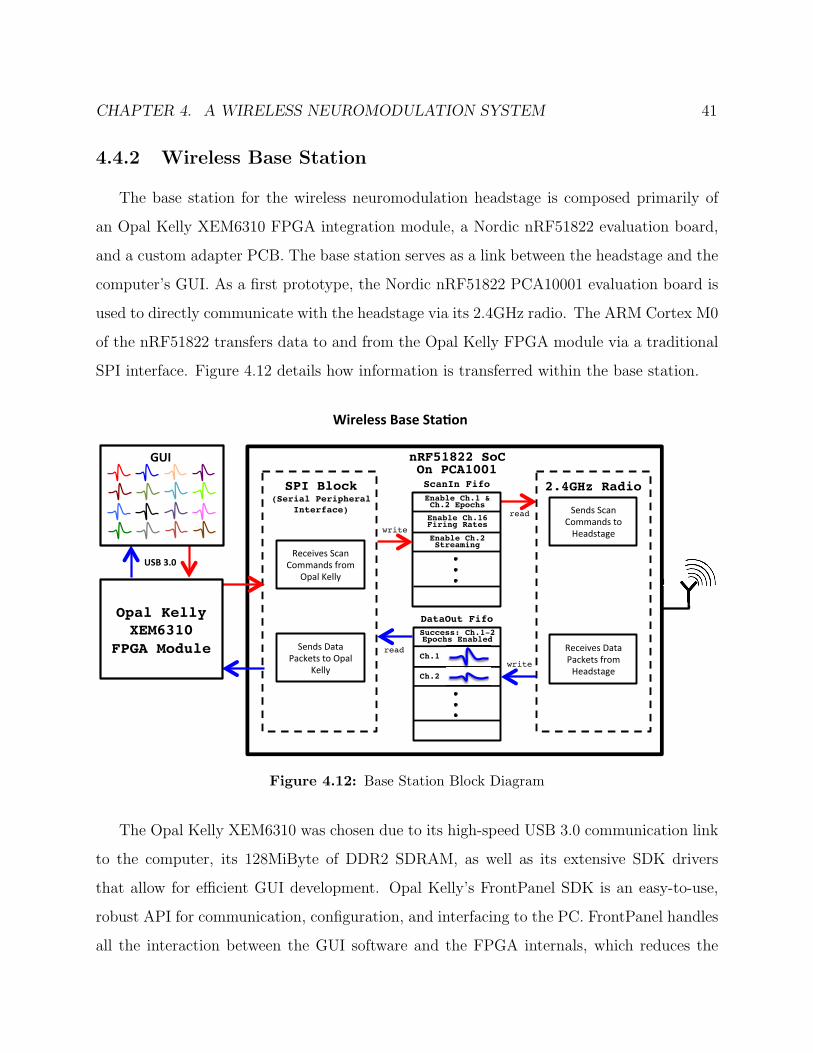
4.4.2 Wireless Base Station
The base station for the wireless neuromodulation headstage is composed primarily of
an Opal Kelly XEM6310 FPGA integration module, a Nordic nRF51822 evaluation board,
and a custom adapter PCB. The base station serves as a link between the headstage and the
computer’s GUI. As a first prototype, the Nordic nRF51822 PCA10001 evaluation board is
used to directly communicate with the headstage via its 2.4GHz radio. The ARM Cortex M0
of the nRF51822 transfers data to and from the Opal Kelly FPGA module via a traditional
SPI interface. Figure 4.12 details how information is transferred within the base station.
DataOut Fifo!
ScanIn Fifo!Enable Ch.1 & Ch.2 Epochs!
Enable Ch.16 Firing Rates!
Enable Ch.2 Streaming!
2.4GHz Radio!
Success: Ch.1-2 Epochs Enabled!
Ch.1!
Ch.2!
SPI Block!(Serial Peripheral
Interface)!
nRF51822 SoC!On PCA1001!
write!
write!
read!
read!
!"#$%&!'(#&)*++(#$%&,*&-"($%,(."&
/"'"01"%&2(,(&3('4",%&56*+&-"($%,(."&
/"'"01"%&!'(#&)*++(#$%&56*+&
78(9&:"99;&
!"#$%&2(,(&3('4",%&,*&78(9&
:"99;&
Opal Kelly!XEM6310!
FPGA Module!
!"#$
"%&$'()$
*+,-.-//$&0/-$%10234$
Figure 4.12: Base Station Block Diagram
The Opal Kelly XEM6310 was chosen due to its high-speed USB 3.0 communication link
to the computer, its 128MiByte of DDR2 SDRAM, as well as its extensive SDK drivers
that allow for efficient GUI development. Opal Kelly’s FrontPanel SDK is an easy-to-use,
robust API for communication, configuration, and interfacing to the PC. FrontPanel handles
all the interaction between the GUI software and the FPGA internals, which reduces the

CHAPTER 4. A WIRELESS NEUROMODULATION SYSTEM 42
time and effort required to interface to a design. The XEM6310 includes a Xilinx Spartan-6
XC6SLX45-2FGG FPGA, and Verilog code was designed in the Xilinx ISE Design Suite.
4.4.3 Computer Graphical User Interface for the WirelessSystem
The user will interact with the wireless headstage through a custom Wireless Biology
Graphical User Interface (WiBi GUI) designed using the Qt Creator Integrated Development
Environment with C++. The Wibi GUI allows the user to program the ASIC wirelessly,
send stimulation commands, and view up to 64 channels each of raw neural data streams,
epochs, and firing rates.

43
Chapter 5
Experimental Results
5.1 In Vivo Rat Testing
To validate the wired headstage system in vivo, extracellular recordings were performed
using a 16-channel microwire array implanted in the visual cortex of an adult Long-Evans
rat. Arrays consisted of teflon-coated tungsten microwires (35µm diameter, 250µm electrode
spacing, 250µm row spacing; Innovative Neurophysiology, Inc., Durham, NC, USA). All
animal procedures were conducted by Ryan Neely in Professor Jose Carmena’s lab and were
approved by the UC Berkeley Animal Care and Use Committee. Extracellular recordings
were performed for several consecutive days, more than one month after the surgery. Clearly
identified waveforms with a high signal-to-noise ratio were chosen for further investigation
as single unit responses. Putative single units were validated based on waveform shape,
reproducibility, amplitude, and duration.
A typical subset of recorded in vivo data is shown in Figure 5.1, which displays time-
aligned epochs recorded from one channel. In order to verify in vivo compression accuracy,
all three forms of the SoC’s outputs were aligned in time, as displayed in Figure 5.2. Each
epoch data packet includes a time stamp, which allows for spike detection confirmation
when superimposed onto the raw data stream. In addition, accurate firing rate calculations
were verified by ensuring that the firing rate counter incremented with each spike event. As
described previously, the SoC computes firing rates over a specified window of time, which
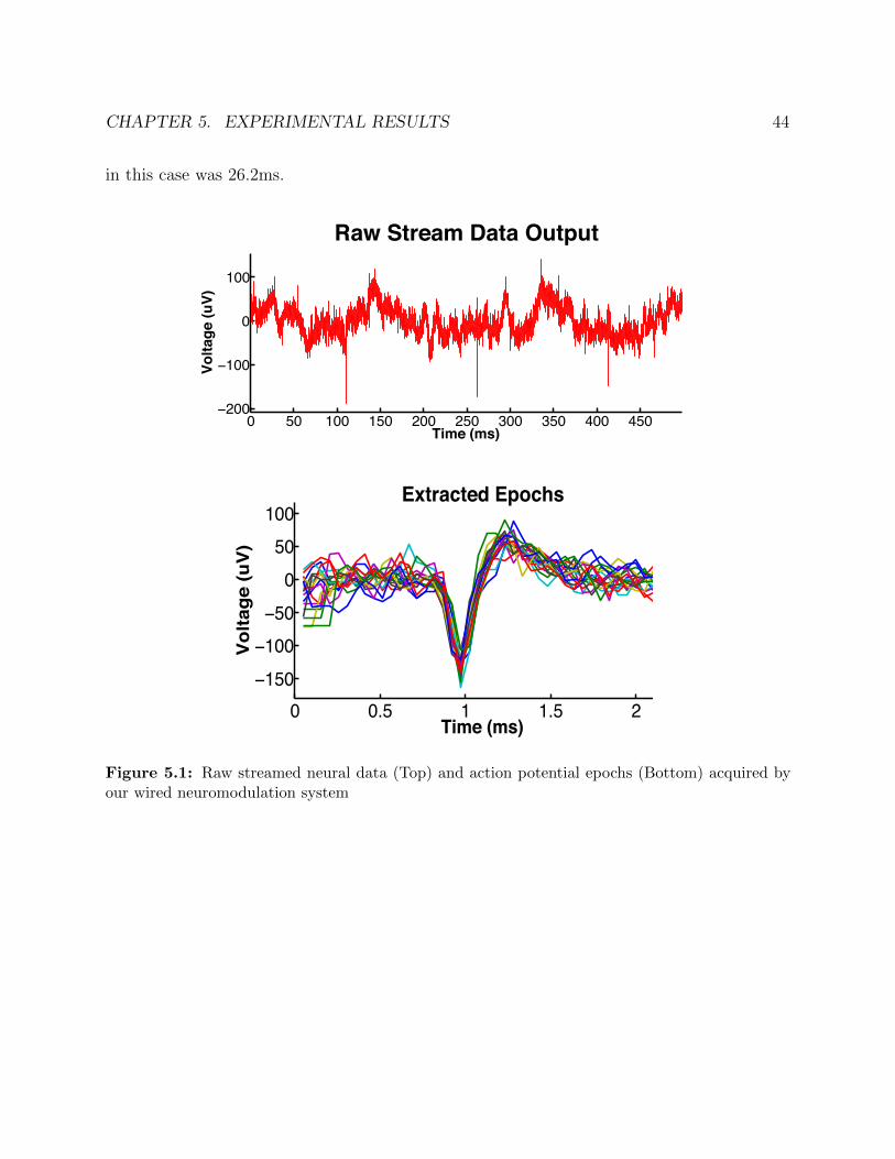
CHAPTER 5. EXPERIMENTAL RESULTS 44
in this case was 26.2ms.
0 50 100 150 200 250 300 350 400 450−200
−100
0
100
Time (ms)
Volta
ge (u
V)
Raw Stream Data Output
0 0.5 1 1.5 2−150−100−50050100
Time (ms)
Vol
tage
(uV
)
Extracted Epochs
Figure 5.1: Raw streamed neural data (Top) and action potential epochs (Bottom) acquired byour wired neuromodulation system

CHAPTER 5. EXPERIMENTAL RESULTS 45
−!""
"
!"" #$%$&'(%)(%*
−!""
"
!""
+,-%$./&0(+1
" 2"" 3"" 4"""
2
3
5)67/
8,(9%*
:6;/&0;*1!"#$%&#'(%
)*+,-
.$%&/
)(%
)*+,-
.$%&/
)(%
0"1"2
.%3-
,$%
&456
786#
'(%
3-9%:-,-%;<,=<,%
>=*?@%;<,=<,%
A="B$%:$,$?,*1%;<,=<,%
&6786#'%C"2D*9'(%
−!""
−#$"
−#""
−$"
"
$"
#""
#$"
!""
!$"
%&'()*+,-.%/
EFF% 6FF% GFF%
Figure 5.2: Raw streams, epochs, and firing rates of in vivo recorded data.
In vivo stimulation was performed in the rat’s visual cortex with a 210µA differential
current for 125µs per phase using the wired system. Stimulation artifacts are shown across
multiple channels in Figure 5.3, and the relative amplitude correlates with proximity to
the stimulation site. It is important to note that the recorded artifact was a differential
measurement referenced to the labeled Ref electrode. In this orientation, the electrodes
closest to the stimulation sites (CH1, CH2, and CH11) should exhibit the highest amplitude
artifact while the furthest channels (CH3, CH4, and CH12) exhibit minimal artifact due
to the localized nature of the differential stimulation. Figure 5.3 also indicates that the
amplifier recovery time is <1ms after stimulation.
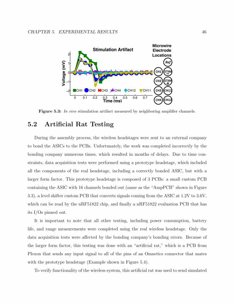
CHAPTER 5. EXPERIMENTAL RESULTS 46
Microwire Electrode Locations"
0 0.1 0.2 0.3 0.4 0.5 0.6 0.7 0.8
−2
−1
0
1
2
Time (ms)
Volta
ge (m
V)
Stimulation Artifact
CH1 CH2 CH3 CH4 CH12 CH11
CH4
CH3
CH2
CH1
CH11
CH12 CH12
STIM
STIM
Ref
Figure 5.3: In vivo stimulation artifact measured by neighboring amplifier channels.
5.2 Artificial Rat Testing
During the assembly process, the wireless headstages were sent to an external company
to bond the ASICs to the PCBs. Unfortunately, the work was completed incorrectly by the
bonding company numerous times, which resulted in months of delays. Due to time con-
straints, data acquisition tests were performed using a prototype headstage, which included
all the components of the real headstage, including a correctly bonded ASIC, but with a
larger form factor. This prototype headstage is composed of 3 PCBs: a small custom PCB
containing the ASIC with 16 channels bonded out (same as the “AmpPCB” shown in Figure
3.3), a level shifter custom PCB that converts signals coming from the ASIC at 1.2V to 3.6V,
which can be read by the nRF51822 chip, and finally a nRF51822 evaluation PCB that has
its I/Os pinned out.
It is important to note that all other testing, including power consumption, battery
life, and range measurements were completed using the real wireless headstage. Only the
data acquisition tests were affected by the bonding company’s bonding errors. Because of
the larger form factor, this testing was done with an “artificial rat,” which is a PCB from
Plexon that sends any input signal to all of the pins of an Omnetics connector that mates
with the prototype headstage (Example shown in Figure 5.4).
To verify functionality of the wireless system, this artificial rat was used to send simulated
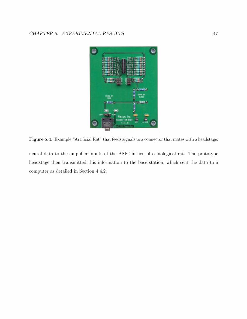
CHAPTER 5. EXPERIMENTAL RESULTS 47
Figure 5.4: Example “Artificial Rat” that feeds signals to a connector that mates with a headstage.
neural data to the amplifier inputs of the ASIC in lieu of a biological rat. The prototype
headstage then transmitted this information to the base station, which sent the data to a
computer as detailed in Section 4.4.2.

48
Chapter 6
Conclusion and Future Work
In this thesis, we have explored the development of a wireless neuromodulation system
capable of 32 channels of real-time neural recording, on-chip data compression, and dual
electrical or optical stimulation on 8 selectable channels, hence offering substantially en-
hanced functionality over current state of the art (e.g. [7, 17, 3]). This wireless headstage
has achieved an effective communication range of 14 meters with a packet error rate of 0.1%
as well as a battery life of 10 hours while constantly transmitting data. Weighing only 4.8
grams and dimensioned at 9mm x 16mm x 29mm, this headstage offers the most features
for its size. Since the bulk of the wireless headstage’s weight is a 110mAh battery, its total
weight can be easily optimized based on the weight and battery life requirements of the
application.
While the current consumption, battery life, and range measurements were performed on
the actual headstage, the data acquisition tests were completed with a prototype headstage
since the bonding company did not correctly bond the ASIC’s amplifier pins on the real
headstage. Once more ASICs are taped out, the real headstage should be sent to another
company for bonding. Because this would not require changing the firmware, software, or
PCB design, the full system using the real headstage will be operational once bonding has
been completed successfully.
The next step in optimizing the design of this wireless headstage is to further reduce its
size. Primarily, we can reduce the area occupied by the chip antenna. In this first prototype,

CHAPTER 6. CONCLUSION AND FUTURE WORK 49
a larger chip antenna with high gain as well as a conservative antenna layout was chosen
to ensure that target range specifications were met. However, since we have confirmed this
design exceeds our requirements, we can move towards a smaller chip antenna, and since the
antenna occupies 30% of the board area, we can significantly reduce overall dimensions.
Another improvement of this headstage will be increasing the number of available record-
ing channels to 64, which is the maximum number that the ASIC can support. 64 channels
is better suited for larger animals, such as monkeys, since there are fewer size and weight
restrictions for head-mounted devices. This thesis’ target application was rat and mouse
research, so 32 channels was a suitable choice, but another 32 channels can be easily added
to the printed circuit board at the cost of area and weight.
In addition to improving hardware, the firmware can be adjusted to read from more than
one headstage. The Base Station’s Nordic 2.4GHz radio currently communicates with just
one headstage, but it is capable of communicating with up to 8 connected devices, and only
the firmware needs to be changed to do this. This would enable unique experiments ana-
lyzing interactions between multiple animals without tangling wires. Furthermore, multiple
headstages could be used on a single animal in order to record or stimulate in unique areas
of the brain while the animal is untethered and free-roaming.
By designing this wireless neuromodulation headstage to be lightweight, ultra low power,
compact, and inconspicuous, we are another step closer to the goal of a clinically viable
wireless Brain Machine Interface that has the potential to restore motor function to patients
suffering from amputation or paralysis and to ultimately free them from the shackles of their
diseases.

50
Bibliography
[1] S.K. Arfin and R. Sarpeshkar. “An Energy-Efficient, Adiabatic Electrode StimulatorWith Inductive Energy Recycling and Feedback Current Regulation”. In: BiomedicalCircuits and Systems, IEEE Transactions on 6.1 (Feb. 2012), pp. 1–14. issn: 1932-4545. doi: 10.1109/TBCAS.2011.2166072.
[2] M. Azin et al. “A Battery-Powered Activity-Dependent Intracortical MicrostimulationIC for Brain-Machine-Brain Interface”. In: Solid-State Circuits, IEEE Journal of 46.4(Apr. 2011), pp. 731–745. issn: 0018-9200. doi: 10.1109/JSSC.2011.2108770.
[3] David Ball et al. “Rodent Scope: A User-Configurable Digital Wireless TelemetrySystem for Freely Behaving Animals”. In: PLoS ONE 9.2 (Feb. 2014), e89949. doi:10.1371/journal.pone.0089949. url: http://dx.doi.org/10.1371/journal.pone.0089949.
[4] Frederic D. Broccard et al. “Closed-Loop Brain-Machine-Body Interfaces for Nonin-vasive Rehabilitation of Movement Disorders”. English. In: Annals of Biomedical En-gineering 42.8 (2014), pp. 1573–1593. issn: 0090-6964. doi: 10.1007/s10439-014-1032-6. url: http://dx.doi.org/10.1007/s10439-014-1032-6.
[5] Jose M Carmena et al. “Learning to Control a Brain-Machine Interface for Reach-ing and Grasping by Primates”. In: PLoS Biol 1.2 (Oct. 2003), e42. doi: 10.1371/journal.pbio.0000042. url: http://dx.doi.org/10.1371/journal.pbio.
0000042.
[6] Tung-Chien Chen et al. “A biomedical multiprocessor SoC for closed-loop neuropros-thetic applications”. In: Solid-State Circuits Conference - Digest of Technical Papers,2009. ISSCC 2009. IEEE International. Feb. 2009, 434–435, 435a. doi: 10.1109/
ISSCC.2009.4977494.
[7] David Fan et al. “A wireless multi-channel recording system for freely behaving miceand rats”. In: PloS one 6.7 (2011), e22033.
[8] Texas Instruments. CC3200 SimpleLink Wi-Fi and Internet-of-Things Solution, a Sin-gle Chip Wireless MCU. 2014. url: http://www.ti.com/product/CC3200/datasheet(visited on 10/20/2014).

BIBLIOGRAPHY 51
[9] V. Karkare, S. Gibson, and D. Markovic. “A 130uW, 64-channel spike-sorting DSPchip”. In: Solid-State Circuits Conference, 2009. A-SSCC 2009. IEEE Asian. Nov.2009, pp. 289–292. doi: 10.1109/ASSCC.2009.5357255.
[10] Wen-Sin Liew, Xiaodan Zou, and Yong Lian. “A 0.5V 1.13uW/channel neural recordinginterface with digital multiplexing scheme”. In: ESSCIRC (ESSCIRC), 2011 Proceed-ings of the. Sept. 2011, pp. 219–222. doi: 10.1109/ESSCIRC.2011.6044946.
[11] Adafruit LLC. Li-Ion and LiPoly Batteries Voltages. 2012. url: https://learn.
adafruit.com/li-ion-and-lipoly-batteries/voltages (visited on 09/01/2014).
[12] Hyo-Gyuem Rhew et al. “A wirelessly powered log-based closed-loop deep brain stim-ulation SoC with two-way wireless telemetry for treatment of neurological disorders”.In: VLSI Circuits (VLSIC), 2012 Symposium on. June 2012, pp. 70–71. doi: 10.1109/VLSIC.2012.6243794.
[13] Tobi A. - Szuts et al. “A wireless multi-channel neural amplifier for freely movinganimals”. In: Nature Neuroscience 14.2 (Feb. 2011), pp. 263–269.
[14] S. Venkatraman and J.M. Carmena. “Active Sensing of Target Location Encoded byCortical Microstimulation”. In: Neural Systems and Rehabilitation Engineering, IEEETransactions on 19.3 (June 2011), pp. 317–324. issn: 1534-4320. doi: 10.1109/TNSRE.2011.2117441.
[15] Johan Wessberg et al. “Real-time prediction of hand trajectory by ensembles of corticalneurons in primates”. In: Nature 408.6810 (2000), pp. 361–365.
[16] D Yeager et al. “A 4.78 mm2 fully-integrated neuromodulation SoC combining 64acquisition channels with digital compression and simultaneous dual stimulation”. In:VLSI Circuits Digest of Technical Papers, 2014 Symposium on. IEEE. 2014, pp. 1–2.
[17] Dian Zhang et al. “A Radio-Telemetry System for Navigation and Recording NeuronalActivity in Free-Roaming Rats”. In: Journal of Bionic Engineering 9.4 (2012), pp. 402–410. issn: 1672-6529. doi: http://dx.doi.org/10.1016/S1672-6529(11)60137-6.url: http://www.sciencedirect.com/science/article/pii/S1672652911601376.