a high-speed & high-capacity single-chip copper ... - ncsu
TRANSCRIPT

A High-Speed & High-CapacitySingle-Chip Copper Crossbar
-Phase Two Report, SRC Copper Design Challenge-
Team members: John DamianoBruce DuewerAlan GlaserToby SchafferJohn Wilson
Lead Faculty: Dr. Paul Franzon
Affiliation: North Carolina State University
Contact: John DamianoRm. 438, EGRC, 1010 Main Campus Dr.North Carolina State UniversityRaleigh, NC 27695-7914(919) 513-2016
Summary
Our UMC Copper Challenge parts did not contain any functional die.Extensive electrical and physical characterization revealed the source ofour non-functioning die. It was found that our diffusion (active) layer datawas omitted from the P20 reticle during mask prep at UMC. Althoughthis omission precludes our team from having functional parts, the failureanalysis performed on the Copper Challenge die yielded important infor-mation about the UMC 0.18m process, and this work is described in theattached report.
Note: This report is available on the Web at http://www.ece.ncsu.edu/erl/copper

Damiano et al.: A High-Speed & High-Capacity Single-Chip Copper Crossbar - Phase Two Report
Background
In our Copper Challenge Phase One report [1], we described the advantages of cop-
per interconnect for a custom crossbar circuit. Using a novel design and a series of
HSPICE simulations, we demonstrated that the use of copper interconnect not only
provides performance enhancements in a state-of-the-art circuit, but that design
trade-offs make copper technology attractive for embedded applications. Compared
to conventional aluminum interconnect technology, our crossbar design with copper
interconnect is 30% faster and displays 15% less latency. We also demonstrated that
the use of copper interconnect provides additional design advantages. Copper inter-
connect allows use of a 40% smaller crossbar cell, offering higher performance with a
substantially smaller die size. Features such as high performance and smaller die
size make copper technology particularly attractive for future design solutions. A
summary of our Phase One Results is shown below in Table I.
Table I. Summary of Phase One Simulation Results for Copper Crossbar
Our design was fabricated by UMC and the initial set of die were delivered to NCSU
on June 27, 2000. The following report is a discussion of our physical and electrical
characterization of the Copper Crossbar circuit since that date.
Parameter Copper Aluminum Improvement
Maximum Data Rate 5.3 GHz 4.0 GHz 30%
Latency 370 ps 425 ps 15%
Cell area 110.8 µm2 181.3 µm2 40%
Input Line Capacitance 705 fF 1478 fF 52%
Output Line Capacitance, final stage 77 fF 112 fF 34%
2

Damiano et al.: A High-Speed & High-Capacity Single-Chip Copper Crossbar - Phase Two Report
Characterization of the Copper Crossbar
The specific goals of our Phase II efforts were to demonstrate three things: the high
frequency performance of our design, the functionality of the small crossbar cell, and
the various novel features of the circuit. The most important of these goals was the
high-frequency characterization since this is directly impacted by the choice of inter-
connect material. Our electrical and physical characterization was directed with
these goals in mind, and our results are detailed below.
Electrical Characterization
Our first effort was to screen the parts for opens and shorts. UMC provided the parts
in two shipments, presumably from different lots. The first set of parts displayed a
substantial number of opens/shorts failures, while the second set of parts was much
better. These results are summarized in Table 2 below.
Table 2. Screening results for Copper Crossbar die
Parts passing the open/shorts tests were deemed "potential yield" while the failing
parts were omitted from further testing. Die passing "opens/shorts" testing were
tested for functionality, and die were deemed functional if input signals were received
at the proper output pins. Unfortunately, zero parts were found to be functional
from either shipment. No output was observed on any output pins for any input sig-
nal. In fact, the only semblance of a signal seen at the output pins was clearly the
Bin First UMC shipment Second UMC shipment
SHORTS 21/39 (54%) 6/45 (13%)
OPENS 1/39 (2%) 0/45 (0%)
PASSING 17/39 (44%) 39/45 (87%)
3
Damiano et al.: A High-Speed & High-Capacity Single-Chip Copper Crossbar - Phase Two Report
result of inductive/capacitive coupling, as shown in Figure 1. Other electrical results
were equally confounding. All on-chip VDD and VSS pins were connected correctly
(i.e. VDD pins were shorted together and VSS pins were shorted together, and NOT
shorted to each other), but the anticipated diode action was not present when the n-
well / p-substrate junction was forward-biased. These results are displayed in Figure
2. Moreover, powered parts displayed a low total current draw compared to simula-
tions (<1mA measured vs. several mA simulated).
In summary, although no obvious failure mode was noted, ALL parts were non-func-
tional and several unusual electrical signatures were observed. These results
directed the second phase of our characterization efforts - the physical characteriza-
tion and failure analysis of our die.
Physical Characterization and Failure Analysis
The physical characterization of our parts was guided by our desire to explain the
poor results seen during electrical characterization. Several die were cleaved in the
X- and Y-direction, stained with BOE (buffered oxide etch) to highlight the various pro-
cess layers, and inspected using a scanning electron microscope. The results of this
inspection are shown in Figures 3 and 4. In each figure, the SEM cross-section is
shown beside the relevant layout data, with the cleave line indicated.
From the SEM results, it can be seen that the metal5 and metal6 layers are approxi-
mately 50% thinner than anticipated [2]. UMC later revealed that their integration
team had chosen to use thinner metal5 and metal6 to enable yield of under-sized vias
on the via4 and via5 levels. The thinner metals, however, are unlikely to cause our
electrical yield signature (the expected performance degradation for our design
resulting from thinner metal5 / metal6 is discussed in Appendix A). Although the use
of three via sizes (0.28x0.28µm and 0.40x0.40µm in the pads, and 0.56x0.56µm else-
4

Damiano et al.: A High-Speed & High-Capacity Single-Chip Copper Crossbar - Phase Two Report
where) on a single level is generally NOT recommended, the redundant vias in the
pads and the lithographic advantages of thinner M5/M6 enabled yield on these levels.
This yield was confirmed electrically on our die, since the connections observed
between the common VDD (and VSS) pads would not be possible without functional
vias on the via4 / via5 levels. The other layers visible in Figures 3 and 4 appear to
have the correct thickness, and the various metal lines have the correct dimensions.
The gate and diffusion layers were obscured in the cleave. No obvious failure modes
are visible in the SEM cross-sections.
As a follow-up to the SEM cross-sections, we also de-processed several die down to
the substrate using concentrated hydrofluoric acid. The results are shown in Figures
5 - 9. Each photo of the substrate is shown with a plot of the associated layout data,
as described in the captions. A serious problem with our chips is readily visible in the
photos - the diffusion pattern (P20) is missing! The diffusion fill layer, consisting of
an array of rectangular diffusion shapes surrounding the missing layout data, is visi-
ble across the circuit area, but the actual diffusion shapes required to form active
devices are not present. We believe that this error occurred during the mask prep
process, specifically during the generation of fill shapes for the P20 reticle. The fill
shape generation process for the P20 reticle is illustrated in Figure 10. Unfortunately,
it appears that the final step in the process was ignored for our die, and that the diffu-
sion data was NOT added back to the reticle data following fill shape generation.
Data provided by team #16 indicates that this error may be limited to our (Team #38)
die. Figure 9 shows a similar pad area located within each team’s design. It can be
seen that while diffusion shapes are visible in Team #16’s layout, the same area
within our die is missing the active. Additional SEMs are shown in Figures 11-12.
Our design cannot work without transistors, and transistors cannot work without a dif-
fusion layer. It appears that our diffusion layer was compromised during the mask
prep process. UMC has agreed to re-order the P20 reticle to include the correct diffu-
5

Damiano et al.: A High-Speed & High-Capacity Single-Chip Copper Crossbar - Phase Two Report
sion pattern for our design. This new reticle will enable us to have working transistors
in our design and yield functional die. We salute UMC for acknowledging the prob-
lem, responding to our request for a new reticle, and choosing to fabricate a follow-up
Copper Challenge wafer start incorporating several process and design adjustments.
While our team was NOT pleased to discover the missing diffusion layer, we were sat-
isfied that our methodical electrical and physical characterization did reveal the
source of our dysfunctional chips. We are confident that the new P20 reticle will
enable production of functional copper crossbar circuits, and we look forward to dem-
onstrating the advantages of copper interconnect using our design.
Summary
Our UMC Copper Challenge parts did not contain any functional die. Extensive elec-
trical and physical characterization revealed the source of our non-functioning die. It
was found that our diffusion (active) layer data was omitted from the P20 reticle dur-
ing mask prep. Although this omission precludes our team from having functional
parts, the failure analysis performed on the Copper Challenge die yielded important
information about the UMC 0.18m process.
Acknowledgments
The authors would like to thank John Phillips of the NCSU SEM Lab for his assis-
tance with sample inspection, and David Nackashi for collaborations during the phys-
ical characterization of samples.
References
[1] “A High-Speed & High-Capacity Single-Chip Copper Crossbar”, J. Damiano, et al.,
submission to SRC Copper Challenge, Dec. 1999. The report is available at
http://www.ece.ncsu.edu/erl/copper .
[2] “SPEC No:G-04-LOGIC18-1P6M-COPPER/LK-INTERCAP”, UMC Group, Rev. 0.1,
1999.
6

Damiano et al.: A High-Speed & High-Capacity Single-Chip Copper Crossbar - Phase Two Report
Appendix “A” - The Impact of Thin Metal5on the Copper Crossbar Design
As mentioned above, the choice was made to use thin metal5 and metal6 layers to com-
pensate for sub-nominal via4 and via5 shapes found in the pad cell layout. Specifically,
0.28x0.28µm and 0.40x0.40µm were found in the Artisan pad cells, while the design
rules specified 0.56x0.56µm vias exclusively. The process issue was “solved” by choos-
ing thin metal5 / metal6 layers (0.45µm vs. 1.0µm in the spec sheet) to mitigate via level
lithography, but it’s worth noting that this choice can degrade the performance of the cir-
cuit, especially if long interconnects are used on the impacted layers.
In our design, the long input lines are routed on metal5 to take advantage of its low sheet
resistance. Therefore, thinning this layer would roughly double the resistance of the
crossbar input lines. Although our performance was chiefly limited by the performance of
the output OR-tree [1], doubling the resistance will degrade our overall circuit perfor-
mance. A simulation was performed to compare a circuit with the original metal5 specs
to one with 2x higher resistance - the results are shown in Figure 13. It can be seen that
the increasing the resistance of the input line increases the load on the driver, and rise
time increases 65% from 89ps to 147ps. The maximum data rate also suffers when thin-
ner metal is used. It can be seen that while the original circuit functioned for input signal
frequencies up to 2.65GHz, the circuit with thin metal fails at 2.5GHz.
While modifying the thickness of process layers can ease integration and improve yield, it
is worth understanding the impact of this choice on the design. For the Copper Crossbar
design, thinner metal5 degrades performance, and the integration team should consider
this trade-off when choosing a final process.
7

Damiano et al.: A High-Speed & High-Capacity Single-Chip Copper Crossbar - Phase Two Report
8
Figure 1. Top: Sample waveform at input pins. Bottom: Measurement at output pinsfor input waveform shown above. Voltage spikes occur at each input transition, mostlikely the capacitive and/or inductive coupling between the input and output leads.

Damiano et al.: A High-Speed & High-Capacity Single-Chip Copper Crossbar - Phase Two Report
9
Figure 2. Top: I-V plot confirming electrical shorts within each set of VDD and VSS
pins, as anticipated (compliance set at 100mA) Bottom: I-V plot displaying theabsence of diode action or voltage protection between VDD and VSS pins. It can
be seen that the current is very low despite the forward-biased n-well/p-substratediode when VDD is <-1V.

Damiano et al.: A High-Speed & High-Capacity Single-Chip Copper Crossbar - Phase Two Report
Figure 3. Top - SEM micrograph of Crossbar Chip from a horizontal cleave throughthe Crossbar Cell array. Bottom - approximate location of SEM cleave on theCrossbar Cell layout. The contacts in the SEM photo are a row of substrate ties.
10

Damiano et al.: A High-Speed & High-Capacity Single-Chip Copper Crossbar - Phase Two Report
Figure 4. Top - SEM micrograph of Crossbar Chip from a vertical cleave through theCrossbar Cell array. Wide input lines on metal 5 are easily seen. Bottom -approximate location of SEM cleave on the Crossbar Cell layout.
11

Damiano et al.: A High-Speed & High-Capacity Single-Chip Copper Crossbar - Phase Two Report
Figure 5. Top - Photo of Crossbar Chip substrate in pad ring illustrating P20 fillshapes and missing diffusion pattern. Bottom - Cadence layout data for padring. P20 diffusion pattern is colored green in the layout.
12

Damiano et al.: A High-Speed & High-Capacity Single-Chip Copper Crossbar - Phase Two Report
Figure 6. Top - Photo of Crossbar Chip substrate in pad circuitry illustrating P20 fillshapes and missing diffusion pattern. Bottom - Cadence layout data for pad cir-cuit. P20 diffusion pattern is colored green and poly is colored red in the layout.
13

Damiano et al.: A High-Speed & High-Capacity Single-Chip Copper Crossbar - Phase Two Report
Figure 7. Top - Photo of Crossbar Chip substrate in array corner illustrating P20 fillshapes and missing diffusion pattern. Bottom - Cadence layout data for arraycorner. P20 diffusion pattern is colored green in the layout.
14

Damiano et al.: A High-Speed & High-Capacity Single-Chip Copper Crossbar - Phase Two Report
Figure 8. Top - Photo of Crossbar Chip substrate in pad circuit illustrating P20 fillshapes and missing diffusion pattern. Bottom - Cadence layout data for pad.P20 diffusion pattern is colored green in the layout.
15

Damiano et al.: A High-Speed & High-Capacity Single-Chip Copper Crossbar - Phase Two Report
Figure 9. Photo of Crossbar Chip substrate from our die (top) and from NCSU Team#16 (bottom). The photos are of an Artisan pad circuit found in both designs. Itcan be seen that while P20 for team #16 consists of both diffusion layout AND fillshapes, all layout data for our die is missing. Only fill shapes were included on theP20 reticle for our die.
16

Damiano et al.: A High-Speed & High-Capacity Single-Chip Copper Crossbar - Phase Two Report
Figure 10. Illustration of boolean operations for sample fill-shape generation process,from layout data through reticle generation. The authors believe that the layoutdiffusion data (D) was NOT returned to the reticle after the fill shapes were cre-ated (i.e. step 3 was omitted inadvertently, and only fill shapes were placed on theP20 reticle)
Poly (P) and Diffusion (D) layout data
P
D
Array of Fill Shapes (F)
F
1
2
3
upsized (P+D)
F - (upsized (P+D))
P20 reticle data =(F - upsized (P+D) )+ D
17
Damiano et al.: A High-Speed & High-Capacity Single-Chip Copper Crossbar - Phase Two Report
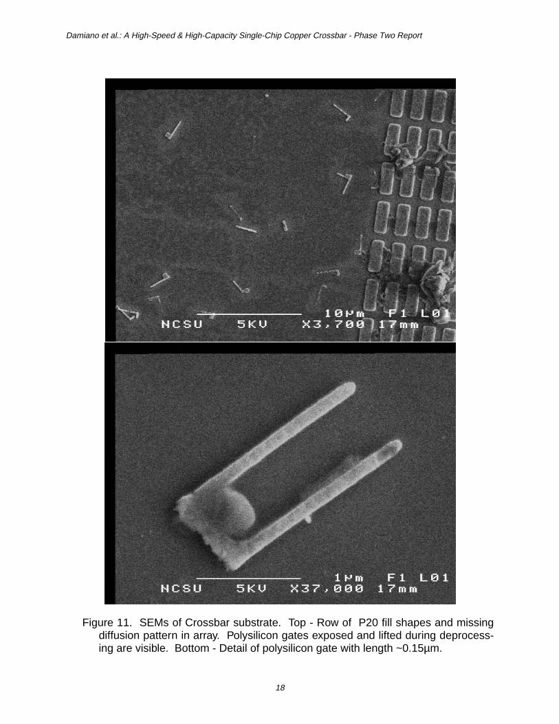
Figure 11. SEMs of Crossbar substrate. Top - Row of P20 fill shapes and missingdiffusion pattern in array. Polysilicon gates exposed and lifted during deprocess-ing are visible. Bottom - Detail of polysilicon gate with length ~0.15µm.
18

Damiano et al.: A High-Speed & High-Capacity Single-Chip Copper Crossbar - Phase Two Report
Figure 12. SEMs of Crossbar substrate. Top - Detail of pad - P20 fill shapes andmissing diffusion pattern are visible. Bottom - Polysilicon gate adjacent to singlediffusion fill feature.
19

Damiano et al.: A High-Speed & High-Capacity Single-Chip Copper Crossbar - Phase Two Report
Figure 13. Simulation data for crossbar circuits with thin and thick metal5. Top: Risetime for input signals increases from 89ps to 147ps when thinner metal5 is used.Bottom: Maximum input signal frequency degrades from 2.65GHz to less than2.5GHz when thinner metal5 is used.
Thickmetal5
Thinmetal5
tr=89ps tr=147ps
20