a high precision, high sample rate digitizer -...
TRANSCRIPT

A high precision, high sample rate digitizer
A. Hidvegi, D. Eriksson, S. Silverstein, B. Cederwall and C. Bohm
Stockholm University and the Royal Institute of Technology (KTH)
Nuclear and Reactor Physics
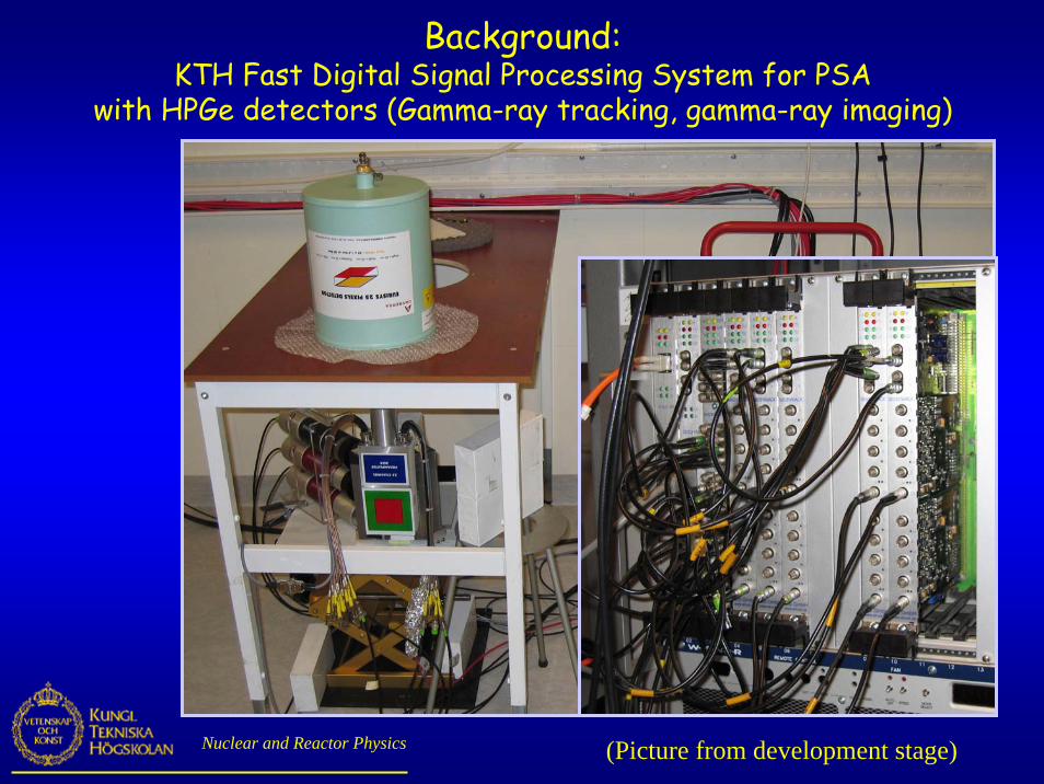
Background:KTH Fast Digital Signal Processing System for PSA
with HPGe detectors (Gamma-ray tracking, gamma-ray imaging)
(Picture from development stage)

Active crystal volume: 50x50x20 mmNuclear and Reactor Physics
25-fold segmented planar pixeldetector @ KTH Stockholm
Manufactured by Canberra EM
Nuclear and Reactor Physics
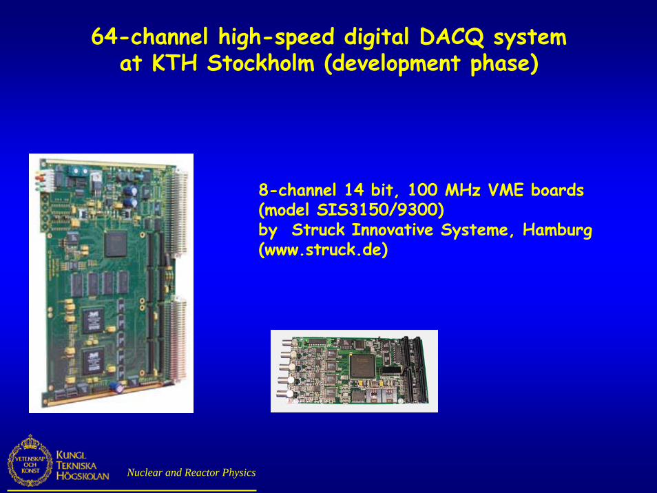
8-channel 14 bit, 100 MHz VME boards(model SIS3150/9300)by Struck Innovative Systeme, Hamburg(www.struck.de)
64-channel high-speed digital DACQ systemat KTH Stockholm (development phase)

Nuclear and Reactor Physics
DACQ architechture
www.struck.de

3D Position Sensitivity
Nuclear and Reactor Physics
depth scan (z)depth scan (z)
lateral scan (y)lateral scan (y)
First, simplified (obvious) Pulse Shape Analysis:Relative amplitudes and timing of both “net charge”and “mirror charge signals
Nuclear and Reactor Physics

Digital n-gamma discrimination in the GHz range
Why digital?
• ” It is possible to take out the maximum amount of information from a detector.
• It is possible to apply any method for signal processing and data evaluation. The choice is limited only by the imagination of the experimentalist, and the useful information in the signal
• It is possible to increase count rate providing successful discrimination and full determination of events separated by a few tens of nanoseconds. ”
• The fast development of processing power and fast sampling ADCs

Digital n-gamma discrimination vs analog
A Kornilov, ... A.J.M. Plompen et al., NIM A497, 467 (03)
B Kaschuk & Y. Esposito, NIM A551, 420 (05)
fast slow

B Kaschuk & Y. Esposito, NIM A551, 420 (05)
Aim : To produce a digitizer with overkill capacity for most applications so that you can be sure that you are well within the
limits with respect to speed, precision and processing power
We have chosen to combine the Atmel AT84AS004 10-bit 2 GHz ADC with 1:2/4 DMUX and a Xilinx Virtex 4 FPGA for readout, signal processing and control
To avoid compromising the performance of the ADC the critical points are:• the design of the analog part• the separation of the analog and digital part• precision and stability of the clock solution
The 500 MHz clock rate between the ADCs and the Xilinx require a careful digital design.We aim to try the 1:2 demultiplexing mode, running at 1 GHz, with 1:4 demultiplexing as a back-up, running at 500 MHz.

We intend to build an 8 channel digitizer, with multi FPGA solution, and gigabit Ethernet communication link with an embedded processor as a controller
To reach this goal we start with exploring the solutions with available evaluation boards while gradually building our own PCB
The evaluation board (AT84AS004-EB) is used to study the ADC in several steps:1) reading the data via a Tektronix logic analyzer2) using a XILINX evaluation board3) using our own FPGA board
We will also design our own ADC board to be studied in a similar way
When the design problems are solved we will merge our ADC design with our FPGA design on one board at first populating only one ADC position (the AT84AS004 are expensive)
Current status: We in the process of studying the the ADC evaluation board with the logic analyzerand we are close to sending away the first FPGA board design for manufacture
We are using Mentor Expedition software for PCB design and simulations

The Atmel AT84AS004evaluation board

Prototype 1
• The FPGA receives data from the AT84AS004-EB through a dedicated port, either with 1:4 demultiplexing @ 500 MHz or 1:2 demultiplexing @ 1 GHz.
• Processed data are sent out through the Gigabit-Ethernet.
• External RAM is available for an embedded system.
Virtex-IV
SX
DRAM
Gb-Ethernet

Prototype 2
• The FPGA receives data directly from two onboard ADCs.
• The aim is to use 1:2 demultiplexing @ 1 GHz, to save pins and routing area. (2 x 20diff = 80 traces)
• Processed data are sent out through the Gigabit-Ethernet.
• External RAM is available for an embedded system.
ADC2 Gsps @ 10-bit
ADC2 Gsps @ 10-bit
Virtex-IV
SX
DRAM
Gb-Ethernet

Prototype 3
• Similar to prototype 2, but here we intend to use up to 8 ADCs.
• Each SX FPGA is handling two ADCs.
• Processed data are sent to the FX FPGA.
• The FX FPGA contains the embedded system, which handles the Gigabit-Ethernet and external memory.
• The embedded system oversees and handles the entire data flow
ADC2 Gsps @ 10-bit
ADC2 Gsps @ 10-bit
Virtex-IV
SX
ADC2 Gsps @ 10-bit
ADC2 Gsps @ 10-bit
Virtex-IV
SX
Virtex-IV
FX
DRAM
Gb-Ethernet