a hidden fingerprint device on an opaque display panel
TRANSCRIPT

applied sciences
Article
A Hidden Fingerprint Device on an OpaqueDisplay Panel
Jhe-Syuan Lin and Wen-Shing Sun *
Department of Optics and Photonics, National Central University, Taoyuan 32001, Taiwan;[email protected]* Correspondence: [email protected]; Tel.: +886-3-4227151 (ext. 65259)
Received: 28 February 2020; Accepted: 16 March 2020; Published: 23 March 2020�����������������
Abstract: In recent years, fingerprint recognition has become more and more widely used in mobilephones. A fingerprint recognition device hidden under an opaque display panel designed based ona waveguide and frustrated total internal reflection (FTIR) is proposed and demonstrated herein.In order to meet the demand for a high screen ratio for mobile phone displays, we use a symmetricalzoom-in and zoom-out coupler design. With this comprehensive coupler and waveguide design,not only can fingerprint recognition be achieved using an opaque display panel, but it also meetsthe appearance requirements for a mobile phone with a high screen ratio.
Keywords: fingerprint recognition; optical waveguide; opaque display panel
1. Introduction
There are several biometric recognition systems that have been developed for applications in mobilephones, such as iris, facial and fingerprint recognition [1,2]. Among them, fingerprint identification isvery important method because of its permanence, uniqueness and reproducibility. It can be achieved byultrasonic [3], capacitive and optical methods [4]. Optical fingerprint recognition (OFR) is the most widelyused in access control systems because of its high image resolution and anti-spoofing capabilities [4–7].However, OFR cannot be used on mobile phones with opaque type displays (such as liquid crystaldisplays, LCDs) due to the following three main reasons. First, the device is hard to integrate into a mobilephone due to its bulkiness [1]. For example, optical coherence tomography (OCT) OFR technology [8] canobtain good quality 3D fingerprint images and information, but complex and large optical architecturesmake it impossible to integrate into mobile phones. Secondly, the backlight module of the LCD panel isopaque, so OFR has difficulty penetrating the LCD panel directly. So far, optical fingerprints can only beused on mobile phones equipped with OLED displays. A wide angle, 3-plastic aspherical lens (totalthickness <4 mm) is placed under the OLED display directly, and then the fingerprint on the screenis taken through this camera. Since the fingerprint image quality is affected by screen obscuration,the fingerprint image must be enhanced by special image processing. Thus, an LCD display phone canonly use capacitive fingerprint unlocking solutions for now.
The last issue is the appearance requirements for a mobile phone with a high screen ratio. Althoughthere are some optical methods to overcome opaque display panels, they cannot meet the requirementsof high screen ratios. Due to the reasons above, capacitive fingerprint methods are only available onopaque display phones [9,10].
In this paper, we have developed a method to overcome these challenges. The integration ofa waveguide into the cover glass of the mobile phone can solve the problem of it not directly beingable to penetrate the opaque display, and the concept of FTIR is applied to the cover glass to enhancethe contrast of the fingerprint image. The concept of combining cover glass and FTIR has been appliedto the design of touch panels [11]. Cameras are used to capture light scattered by the ridge of the finger,
Appl. Sci. 2020, 10, 2188; doi:10.3390/app10062188 www.mdpi.com/journal/applsci

Appl. Sci. 2020, 10, 2188 2 of 8
and image processing techniques are used to detect the position of finger pressing. However, we usethe unscattered light in the cover glass to form the image of finger ridges and valleys. Furthermore,using the concept of optical projection magnification, the light beam diameter can reach the minimumdiameter when entering and exiting the cover glass. This optical design concept can be applied used tomeet the need for a high screen ratio.
2. Theory
A prototype of the proposed OFR that can be integrated into a display is presented in Figure 1a.Light from the collimated light source system [12] is reflected into the cover glass by the reflectivesurface above it, as shown in Figure 1b. The light area is projected onto the reflecting surfaceand changed from A to A′. The formulation is shown in Equation (1). The light is then again projectedby the reflecting surface onto the surface of the cover glass, as shown in Figure 1c, and the relationshipis formulated as in Equation (2). For example, if the width of A is 1 mm and the angle of the reflectivesurface is 38 degrees, the length of A” is about 4.13 mm. This means that we can inject a narrowlight width (A) and get a larger light width (A”) after reflection. Based on this concept we can obtainan effective high screen ratio design. After the light is reflected by the reflecting surface, it is transmittedinto the cover glass with total internal reflection (TIR). When the finger is pressed on the surface ofthe cover glass, the placement of the ridges will destroy the total internal reflection due to changes inthe refractive index. This principle is usually called frustrated total internal reflection (FTIR). In orderto allow the light to have total internal reflection in the cover glass and be partially destroyed whena fingerprint is placed on the cover glass, the angle of the reflective surface must satisfy the conditionin Equation (3), where nskin, ncover glass and nair are the refractive indices of fingerprint skin, cover glassand air, set to 1.5, 1.517 and 1 respectively. Thus, we get the design value of the angle of the reflectionsurface between 20.6 degrees and 40.7 degrees. The remaining total internally reflected light willcontinue to be reflected to the end of the cover glass where there is a reflective surface with the sameangle, which will change the width of A′ back to the width of A. After this, a third reflective surface willbe placed under the cover glass; the function of this reflecting surface is to enlarge the beam to the widthof A′ and project it onto the Complementary Metal Oxide Semiconductor (CMOS) sensor. It is throughthe inclusion of this third reflective surface that we can obtain fingerprints on the CMOS sensor withthe same area as on the cover glass. Through this design, we can create a fingerprint recognition devicethat can be used in opaque displays while meeting the requirement of high screen ratios.
Appl. Sci. 2020, 10, x FOR PEER REVIEW 3 of 9
(a)
(b) (c)
Figure 1. (a) The design concept which combines with the display panel. (b) Light area enlarges from
A to A’ due to θ angle. (c) Light area enlarges from A’ to A’’ due to θ angle.
𝐴′ =𝐴
cos(𝜃) (1)
𝐴′′ = 𝐴 + 𝐴′ ∙ sin(𝜃) ∙ tan(2𝜃) (2)
𝑛𝑠𝑘𝑖𝑛 > 𝑛𝑐𝑜𝑣𝑒𝑟 𝑔𝑙𝑎𝑠𝑠 ∙ sin 2𝜃𝑐𝑜𝑣𝑒𝑟 𝑔𝑙𝑎𝑠𝑠 > 𝑛𝑎𝑖𝑟 (3)
3. Simulation
The CMOS specifications selected for use in this paper are shown in Table 1. The shortest side
of the CMOS is 4 mm, so A’’ must be designed at least larger than this value. From Equation 2, the
width of A’’ is related to the angle of the reflective surface. This relationship is illustrated in Figure 2.
The angle of reflective surface needs to be at least 37.8 degrees from the derivation of Figure 2. For
instance, A 6.5-inch display with a resolution of 1920 1080 has a length of 143.89 cm on the long
side. Therefore, the length of the cover glass must be greater than this value (143.89 cm).
Table 1. Specifications of Complementary Metal Oxide Semiconductor (CMOS).
Item Specification
Sensing Area 4 mm 6 mm
Pixel Size 50 m
Resolution 80 120
Display Panel
Light SourceCMOS
Mirror
Cover Glass
θ
A
A’
θ
H
Light
Source
A’
A’’
θθ
2θA’
θ
θ 2θ
Light
Source
Figure 1. (a) The design concept which combines with the display panel. (b) Light area enlarges fromA to A′ due to θ angle. (c) Light area enlarges from A′ to A” due to θ angle.

Appl. Sci. 2020, 10, 2188 3 of 8
A′ =A
cos(θ)(1)
A′′ = A + A′· sin(θ)· tan(2θ) (2)
nskin > ncover glass· sin 2θcover glass > nair (3)
3. Simulation
The CMOS specifications selected for use in this paper are shown in Table 1. The shortest sideof the CMOS is 4 mm, so A” must be designed at least larger than this value. From Equation (2),the width of A” is related to the angle of the reflective surface. This relationship is illustrated inFigure 2. The angle of reflective surface needs to be at least 37.8 degrees from the derivation of Figure 2.For instance, A 6.5-inch display with a resolution of 1920 × 1080 has a length of 143.89 cm on the longside. Therefore, the length of the cover glass must be greater than this value (143.89 cm).
Table 1. Specifications of Complementary Metal Oxide Semiconductor (CMOS).
Item Specification
Sensing Area 4 mm × 6 mmPixel Size 50 µm
Resolution 80 × 120
Appl. Sci. 2020, 10, x FOR PEER REVIEW 3 of 8
(b) (c)
Figure 1. (a) The design concept which combines with the display panel. (b) Light area enlarges from
A to A’ due to θ angle. (c) Light area enlarges from A’ to A’’ due to θ angle.
𝐴′ =𝐴
cos(𝜃) (1)
𝐴′′ = 𝐴 + 𝐴′ ∙ sin(𝜃) ∙ tan(2𝜃) (2)
𝑛𝑠𝑘𝑖𝑛 > 𝑛𝑐𝑜𝑣𝑒𝑟 𝑔𝑙𝑎𝑠𝑠 ∙ sin 2𝜃𝑐𝑜𝑣𝑒𝑟 𝑔𝑙𝑎𝑠𝑠 > 𝑛𝑎𝑖𝑟 (3)
3. Simulation
The CMOS specifications selected for use in this paper are shown in Table 1. The shortest side
of the CMOS is 4 mm, so A’’ must be designed at least larger than this value. From Equation 2, the
width of A’’ is related to the angle of the reflective surface. This relationship is illustrated in Figure 2.
The angle of reflective surface needs to be at least 37.8 degrees from the derivation of Figure 2. For
instance, A 6.5-inch display with a resolution of 1920 1080 has a length of 143.89 cm on the long
side. Therefore, the length of the cover glass must be greater than this value (143.89 cm).
Table 1. Specifications of Complementary Metal Oxide Semiconductor (CMOS).
Item Specification
Sensing Area 4 mm 6 mm
Pixel Size 50 m
Resolution 80 120
Figure 2. The blue line shows the enlarged relationship between A’’ and the angle of the reflecting
surface. The red line shows the limitation of CMOS.
Considering the above conditions, we chose a suitable design specification, shown in Table 2.
Table 2. Geometric specifications of cover glass.
CG angle CG Thickness CG Length A A’ A’’
39 1 mm 147 mm 1 mm 1.29 mm 4.81 mm
Applying the design value from Table 2, the transmission of light meeting the TIR condition in
the cover glass is shown in Figure 3. The light was reflected 31 times from the top to the end of the
cover glass. Since the light does not meet the TIR conditions on the edge reflective surface, a reflective
coating is needed. The screen ratio is an important value in the appearance standard of mobile
phones. At present, the screen ratio of high-end mobile phones on the market needs to be more than
90%. The definition of screen ratio is shown in Equation 4. Using the cover glass length value given
0
1
2
3
4
5
6
7
8
30 31 32 33 34 35 36 37 38 39 40 41
Wid
th (
mm
)
Angle ()
The Relationship between A'' width and angle
Figure 2. The blue line shows the enlarged relationship between A” and the angle of the reflectingsurface. The red line shows the limitation of CMOS.
Considering the above conditions, we chose a suitable design specification, shown in Table 2.
Table 2. Geometric specifications of cover glass.
CG Angle CG Thickness CG Length A A′ A”
39◦ 1 mm 147 mm 1 mm 1.29 mm 4.81 mm
Applying the design value from Table 2, the transmission of light meeting the TIR condition inthe cover glass is shown in Figure 3. The light was reflected 31 times from the top to the end of the coverglass. Since the light does not meet the TIR conditions on the edge reflective surface, a reflectivecoating is needed. The screen ratio is an important value in the appearance standard of mobile phones.At present, the screen ratio of high-end mobile phones on the market needs to be more than 90%.The definition of screen ratio is shown in Equation (4). Using the cover glass length value given in
Appl. Sci. 2020, 10, 2188 4 of 8
Table 2, for a 6.5-inch display, the screen ratio value obtained with our design can satisfy the demandfor a ratio of more than 90%.
Screen Ratio =Area o f Display
Area o f Cover Glass(4)
Appl. Sci. 2020, 10, x FOR PEER REVIEW 4 of 8
in Table 2, for a 6.5-inch display, the screen ratio value obtained with our design can satisfy the
demand for a ratio of more than 90%.
Screen Ratio = 𝐴𝑟𝑒𝑎 𝑜𝑓 𝐷𝑖𝑠𝑝𝑙𝑎𝑦
𝐴𝑟𝑒𝑎 𝑜𝑓 𝐶𝑜𝑣𝑒𝑟 𝐺𝑙𝑎𝑠𝑠 (4)
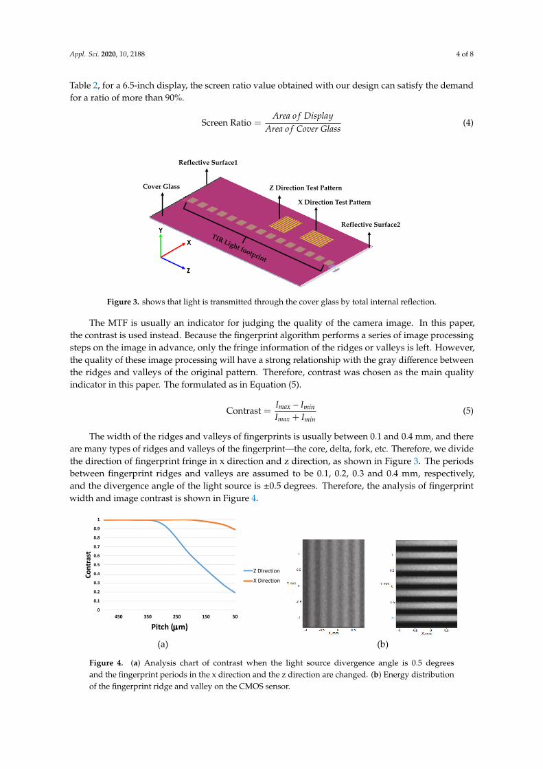
Figure 3. shows that light is transmitted through the cover glass by total internal reflection.
The MTF is usually an indicator for judging the quality of the camera image. In this paper, the
contrast is used instead. Because the fingerprint algorithm performs a series of image processing
steps on the image in advance, only the fringe information of the ridges or valleys is left. However,
the quality of these image processing will have a strong relationship with the gray difference between
the ridges and valleys of the original pattern. Therefore, contrast was chosen as the main quality
indicator in this paper. The formulated as in Equation 5.
Contrast = 𝐼𝑚𝑎𝑥−𝐼𝑚𝑖𝑛
𝐼𝑚𝑎𝑥+𝐼𝑚𝑖𝑛 (5)
The width of the ridges and valleys of fingerprints is usually between 0.1 and 0.4 mm, and there
are many types of ridges and valleys of the fingerprint—the core, delta, fork, etc. Therefore, we divide
the direction of fingerprint fringe in x direction and z direction, as shown in Figure 3. The periods
between fingerprint ridges and valleys are assumed to be 0.1, 0.2, 0.3 and 0.4 mm, respectively, and
the divergence angle of the light source is 0.5 degrees. Therefore, the analysis of fingerprint width
and image contrast is shown in Figure 4.
(a) (b)
Figure 4. (a) Analysis chart of contrast when the light source divergence angle is 0.5 degrees and the
fingerprint periods in the x direction and the z direction are changed. (b) Energy distribution of the
fingerprint ridge and valley on the CMOS sensor.
As can be seen in Figure 4, the contrast in the X direction is higher than the Z direction in the
same fingerprint width, because the X component of the light source angle cannot be incident on the
CMOS sensor, as the transmission distance is longer, as shown in Figure 5 (a). For example, the
divergence angle of the light source is 1 degree, but the angle that can actually be received by the
CMOS sensor is only 0.5 degrees. However, the X component of the light source angle will be incident
Reflective Surface1
Reflective Surface2
Cover Glass
Y
X
Z
Z Direction Test Pattern
X Direction Test Pattern
0
0.1
0.2
0.3
0.4
0.5
0.6
0.7
0.8
0.9
1
50150250350450
Co
ntr
ast
Pitch (m)
Z DIrection
X Direction
Figure 3. shows that light is transmitted through the cover glass by total internal reflection.
The MTF is usually an indicator for judging the quality of the camera image. In this paper,the contrast is used instead. Because the fingerprint algorithm performs a series of image processingsteps on the image in advance, only the fringe information of the ridges or valleys is left. However,the quality of these image processing will have a strong relationship with the gray difference betweenthe ridges and valleys of the original pattern. Therefore, contrast was chosen as the main qualityindicator in this paper. The formulated as in Equation (5).
Contrast =Imax − IminImax + Imin
(5)
The width of the ridges and valleys of fingerprints is usually between 0.1 and 0.4 mm, and thereare many types of ridges and valleys of the fingerprint—the core, delta, fork, etc. Therefore, we dividethe direction of fingerprint fringe in x direction and z direction, as shown in Figure 3. The periodsbetween fingerprint ridges and valleys are assumed to be 0.1, 0.2, 0.3 and 0.4 mm, respectively,and the divergence angle of the light source is ±0.5 degrees. Therefore, the analysis of fingerprintwidth and image contrast is shown in Figure 4.
Appl. Sci. 2020, 10, x FOR PEER REVIEW 4 of 8
in Table 2, for a 6.5-inch display, the screen ratio value obtained with our design can satisfy the
demand for a ratio of more than 90%.
Screen Ratio = 𝐴𝑟𝑒𝑎 𝑜𝑓 𝐷𝑖𝑠𝑝𝑙𝑎𝑦
𝐴𝑟𝑒𝑎 𝑜𝑓 𝐶𝑜𝑣𝑒𝑟 𝐺𝑙𝑎𝑠𝑠 (4)
Figure 3. shows that light is transmitted through the cover glass by total internal reflection.
The MTF is usually an indicator for judging the quality of the camera image. In this paper, the
contrast is used instead. Because the fingerprint algorithm performs a series of image processing
steps on the image in advance, only the fringe information of the ridges or valleys is left. However,
the quality of these image processing will have a strong relationship with the gray difference between
the ridges and valleys of the original pattern. Therefore, contrast was chosen as the main quality
indicator in this paper. The formulated as in Equation 5.
Contrast = 𝐼𝑚𝑎𝑥−𝐼𝑚𝑖𝑛
𝐼𝑚𝑎𝑥+𝐼𝑚𝑖𝑛 (5)
The width of the ridges and valleys of fingerprints is usually between 0.1 and 0.4 mm, and there
are many types of ridges and valleys of the fingerprint—the core, delta, fork, etc. Therefore, we divide
the direction of fingerprint fringe in x direction and z direction, as shown in Figure 3. The periods
between fingerprint ridges and valleys are assumed to be 0.1, 0.2, 0.3 and 0.4 mm, respectively, and
the divergence angle of the light source is 0.5 degrees. Therefore, the analysis of fingerprint width
and image contrast is shown in Figure 4.
(a) (b)
Figure 4. (a) Analysis chart of contrast when the light source divergence angle is 0.5 degrees and the
fingerprint periods in the x direction and the z direction are changed. (b) Energy distribution of the
fingerprint ridge and valley on the CMOS sensor.
As can be seen in Figure 4, the contrast in the X direction is higher than the Z direction in the
same fingerprint width, because the X component of the light source angle cannot be incident on the
CMOS sensor, as the transmission distance is longer, as shown in Figure 5 (a). For example, the
divergence angle of the light source is 1 degree, but the angle that can actually be received by the
CMOS sensor is only 0.5 degrees. However, the X component of the light source angle will be incident
Reflective Surface1
Reflective Surface2
Cover Glass
Y
X
Z
Z Direction Test Pattern
X Direction Test Pattern
0
0.1
0.2
0.3
0.4
0.5
0.6
0.7
0.8
0.9
1
50150250350450
Co
ntr
ast
Pitch (m)
Z DIrection
X Direction
Figure 4. (a) Analysis chart of contrast when the light source divergence angle is 0.5 degreesand the fingerprint periods in the x direction and the z direction are changed. (b) Energy distributionof the fingerprint ridge and valley on the CMOS sensor.
Appl. Sci. 2020, 10, 2188 5 of 8
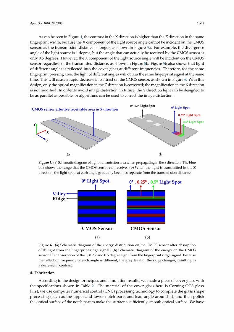
As can be seen in Figure 4, the contrast in the X direction is higher than the Z direction in the samefingerprint width, because the X component of the light source angle cannot be incident on the CMOSsensor, as the transmission distance is longer, as shown in Figure 5a. For example, the divergenceangle of the light source is 1 degree, but the angle that can actually be received by the CMOS sensor isonly 0.5 degrees. However, the X component of the light source angle will be incident on the CMOSsensor regardless of the transmitted distance, as shown in Figure 5b. Figure 5b also shows that lightof different angles is reflected into the cover glass at different frequencies. Therefore, for the samefingerprint pressing area, the light of different angles will obtain the same fingerprint signal at the sametime. This will cause a rapid decrease in contrast on the CMOS sensor, as shown in Figure 6. With thisdesign, only the optical magnification in the Z direction is corrected; the magnification in the X directionis not modified. In order to avoid image distortion, in future, the Y direction light can be designed tobe as parallel as possible, or algorithms can be used to correct the image distortion.
Appl. Sci. 2020, 10, x FOR PEER REVIEW 5 of 8
on the CMOS sensor regardless of the transmitted distance, as shown in Figure 5 (b). Figure 5 (b) also
shows that light of different angles is reflected into the cover glass at different frequencies. Therefore,
for the same fingerprint pressing area, the light of different angles will obtain the same fingerprint
signal at the same time. This will cause a rapid decrease in contrast on the CMOS sensor, as shown
in Figure 6. With this design, only the optical magnification in the Z direction is corrected; the
magnification in the X direction is not modified. In order to avoid image distortion, in future, the Y
direction light can be designed to be as parallel as possible, or algorithms can be used to correct the
image distortion.
(a) (b)
Figure 5. (a) Schematic diagram of light transmission area when propagating in the z direction. The
blue box shows the range that the CMOS sensor can receive. (b) When the light is transmitted in the
Z direction, the light spots at each angle gradually becomes separate from the transmission distance.
(a) (b)
Figure 6. (a) Schematic diagram of the energy distribution on the CMOS sensor after absorption of 0
light from the fingerprint ridge signal. (b) Schematic diagram of the energy on the CMOS sensor after
absorption of the 0, 0.25, and 0.5 degree light from the fingerprint ridge signal. Because the reflection
frequency of each angle is different, the gray level of the ridge changes, resulting in a decrease in
contrast.
4. Fabrication
According to the design principles and simulation results, we made a piece of cover glass with
the specifications shown in Table 2. The material of the cover glass here is Corning GG3 glass. First,
we use computer numerical control (CNC) processing technology to complete the glass shape
processing (such as the upper and lower notch parts and lead angle around it), and then polish the
optical surface of the notch part to make the surface a sufficiently smooth optical surface. We have
optimized the appearance of the reflective surface 1 and the reflective surface 2. Using the notch
design method, the screen utilization can be maximized, as shown in Figure 7. The silver part is
coated with aluminum metal, and a lead angle is added around the cover glass to avoid cracking
during process.
CMOS sensor effective receivable area in X direction
Y
X
Z
0~0.5 Light Spot0 Light Spot
0.25 Light Spot
0.5 Light Spot
0 Light Spot
ValleyRidge
0 , 0.25 , 0.5 Light Spot
CMOS Sensor CMOS Sensor
Figure 5. (a) Schematic diagram of light transmission area when propagating in the z direction. The bluebox shows the range that the CMOS sensor can receive. (b) When the light is transmitted in the Zdirection, the light spots at each angle gradually becomes separate from the transmission distance.
Appl. Sci. 2020, 10, x FOR PEER REVIEW 5 of 8
on the CMOS sensor regardless of the transmitted distance, as shown in Figure 5 (b). Figure 5 (b) also
shows that light of different angles is reflected into the cover glass at different frequencies. Therefore,
for the same fingerprint pressing area, the light of different angles will obtain the same fingerprint
signal at the same time. This will cause a rapid decrease in contrast on the CMOS sensor, as shown
in Figure 6. With this design, only the optical magnification in the Z direction is corrected; the
magnification in the X direction is not modified. In order to avoid image distortion, in future, the Y
direction light can be designed to be as parallel as possible, or algorithms can be used to correct the
image distortion.
(a) (b)
Figure 5. (a) Schematic diagram of light transmission area when propagating in the z direction. The
blue box shows the range that the CMOS sensor can receive. (b) When the light is transmitted in the
Z direction, the light spots at each angle gradually becomes separate from the transmission distance.
(a) (b)
Figure 6. (a) Schematic diagram of the energy distribution on the CMOS sensor after absorption of 0
light from the fingerprint ridge signal. (b) Schematic diagram of the energy on the CMOS sensor after
absorption of the 0, 0.25, and 0.5 degree light from the fingerprint ridge signal. Because the reflection
frequency of each angle is different, the gray level of the ridge changes, resulting in a decrease in
contrast.
4. Fabrication
According to the design principles and simulation results, we made a piece of cover glass with
the specifications shown in Table 2. The material of the cover glass here is Corning GG3 glass. First,
we use computer numerical control (CNC) processing technology to complete the glass shape
processing (such as the upper and lower notch parts and lead angle around it), and then polish the
optical surface of the notch part to make the surface a sufficiently smooth optical surface. We have
optimized the appearance of the reflective surface 1 and the reflective surface 2. Using the notch
design method, the screen utilization can be maximized, as shown in Figure 7. The silver part is
coated with aluminum metal, and a lead angle is added around the cover glass to avoid cracking
during process.
CMOS sensor effective receivable area in X direction
Y
X
Z
0~0.5 Light Spot0 Light Spot
0.25 Light Spot
0.5 Light Spot
0 Light Spot
ValleyRidge
0 , 0.25 , 0.5 Light Spot
CMOS Sensor CMOS Sensor
Figure 6. (a) Schematic diagram of the energy distribution on the CMOS sensor after absorptionof 0◦ light from the fingerprint ridge signal. (b) Schematic diagram of the energy on the CMOSsensor after absorption of the 0, 0.25, and 0.5 degree light from the fingerprint ridge signal. Becausethe reflection frequency of each angle is different, the gray level of the ridge changes, resulting ina decrease in contrast.
4. Fabrication
According to the design principles and simulation results, we made a piece of cover glass withthe specifications shown in Table 2. The material of the cover glass here is Corning GG3 glass.First, we use computer numerical control (CNC) processing technology to complete the glass shapeprocessing (such as the upper and lower notch parts and lead angle around it), and then polishthe optical surface of the notch part to make the surface a sufficiently smooth optical surface. We have

Appl. Sci. 2020, 10, 2188 6 of 8
optimized the appearance of the reflective surface 1 and the reflective surface 2. Using the notch designmethod, the screen utilization can be maximized, as shown in Figure 7. The silver part is coated withaluminum metal, and a lead angle is added around the cover glass to avoid cracking during process.Appl. Sci. 2020, 10, x FOR PEER REVIEW 6 of 8
Figure 7. Cover glass processed according to Table 2 specifications, with lead angles added around
the sides to avoid cracking.
Figure 8 (a) is a cross-sectional view of reflective surface 1. We used Panasonic's Ultrahigh
Accurate 3-D Profilometer (UA3P) to measure the surface condition and angle of the inclined surface.
The result is shown in Figure 8 (b). The angle of the reflecting surface 1 is 39.09 degrees. From the
cross-sectional view of Figure 8 (a), we can see the design of the lead angle on the upper and lower
sides of the bevel. This lead angle design is necessary; otherwise the bevel will be easily broken
during processing. The cross-sectional view of the reflecting surface 2 is shown in Figure 9 (a). In the
design, the angles of the two reflecting surfaces are the same. The actual measured angle using UA3P
is 39.01 degrees. The UA3P cannot measure the lead angle extending inward, so the bottom part of
the measurement chart and the actual section view are different.
(a) (b)
Figure 8. (a) Cross-sectional view of reflection surface 1 of the cover glass. (B) Using UA3P
measurement results, the angle of reflection surface 1 is 39.09 degrees.
(a) (b)
Figure 9. (a) Cross-sectional view of reflection surface 2 of the cover glass. (B) Using UA3P
measurement results, the angle of reflection surface 2 is 39.09 degrees.
Reflective Surface 1
Reflective Surface 2
Y-D
irec
tion
(mm
)
-1
-0.8
-0.6
-0.4
-0.2
0
0.2
-2 -1.5 -1 -0.5 0
Z-Direction (mm)
-1
-0.8
-0.6
-0.4
-0.2
0
0.2
-2.1-1.6-1.1-0.6-0.1
Z-Direction (mm)
Y-D
ire
ctio
n (
mm
)
Figure 7. Cover glass processed according to Table 2 specifications, with lead angles added aroundthe sides to avoid cracking.
Figure 8a is a cross-sectional view of reflective surface 1. We used Panasonic’s Ultrahigh Accurate3-D Profilometer (UA3P) to measure the surface condition and angle of the inclined surface. The resultis shown in Figure 8b. The angle of the reflecting surface 1 is 39.09 degrees. From the cross-sectionalview of Figure 8a, we can see the design of the lead angle on the upper and lower sides of the bevel.This lead angle design is necessary; otherwise the bevel will be easily broken during processing.The cross-sectional view of the reflecting surface 2 is shown in Figure 9a. In the design, the anglesof the two reflecting surfaces are the same. The actual measured angle using UA3P is 39.01 degrees.The UA3P cannot measure the lead angle extending inward, so the bottom part of the measurementchart and the actual section view are different.
Appl. Sci. 2020, 10, x FOR PEER REVIEW 6 of 8
Figure 7. Cover glass processed according to Table 2 specifications, with lead angles added around
the sides to avoid cracking.
Figure 8 (a) is a cross-sectional view of reflective surface 1. We used Panasonic's Ultrahigh
Accurate 3-D Profilometer (UA3P) to measure the surface condition and angle of the inclined surface.
The result is shown in Figure 8 (b). The angle of the reflecting surface 1 is 39.09 degrees. From the
cross-sectional view of Figure 8 (a), we can see the design of the lead angle on the upper and lower
sides of the bevel. This lead angle design is necessary; otherwise the bevel will be easily broken
during processing. The cross-sectional view of the reflecting surface 2 is shown in Figure 9 (a). In the
design, the angles of the two reflecting surfaces are the same. The actual measured angle using UA3P
is 39.01 degrees. The UA3P cannot measure the lead angle extending inward, so the bottom part of
the measurement chart and the actual section view are different.
(a) (b)
Figure 8. (a) Cross-sectional view of reflection surface 1 of the cover glass. (B) Using UA3P
measurement results, the angle of reflection surface 1 is 39.09 degrees.
(a) (b)
Figure 9. (a) Cross-sectional view of reflection surface 2 of the cover glass. (B) Using UA3P
measurement results, the angle of reflection surface 2 is 39.09 degrees.
Reflective Surface 1
Reflective Surface 2
Y-D
irec
tion
(mm
)
-1
-0.8
-0.6
-0.4
-0.2
0
0.2
-2 -1.5 -1 -0.5 0
Z-Direction (mm)
-1
-0.8
-0.6
-0.4
-0.2
0
0.2
-2.1-1.6-1.1-0.6-0.1
Z-Direction (mm)
Y-D
ire
ctio
n (
mm
)
Figure 8. (a) Cross-sectional view of reflection surface 1 of the cover glass. (b) Using UA3P measurementresults, the angle of reflection surface 1 is 39.09 degrees.
An HeNe laser is used to enter the cover glass after expanding and collimating. The characteristicsof total reflection of light in the glass are shown in Figure 10a. From the observations, the beam doesnot diffuse significantly in the X direction due to the HeNe laser being collimated, and both anglecomponents of the light have collimation characteristics. Figure 10b shows the actual pressure ofthe finger. Since the FTIR concept is applied in the design, the finger pressure contrast between ridgesand valleys is clear and easy to recognize. In Figure 10b, the black parts are ridges and the white partsare valleys. In addition, we use infrared LED as the light source. The smaller size of the LED is easier
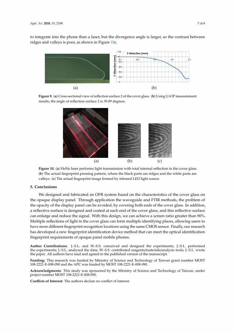
Appl. Sci. 2020, 10, 2188 7 of 8
to integrate into the phone than a laser, but the divergence angle is larger, so the contrast betweenridges and valleys is poor, as shown in Figure 10c.
Appl. Sci. 2020, 10, x FOR PEER REVIEW 6 of 8
Figure 7. Cover glass processed according to Table 2 specifications, with lead angles added around
the sides to avoid cracking.
Figure 8 (a) is a cross-sectional view of reflective surface 1. We used Panasonic's Ultrahigh
Accurate 3-D Profilometer (UA3P) to measure the surface condition and angle of the inclined surface.
The result is shown in Figure 8 (b). The angle of the reflecting surface 1 is 39.09 degrees. From the
cross-sectional view of Figure 8 (a), we can see the design of the lead angle on the upper and lower
sides of the bevel. This lead angle design is necessary; otherwise the bevel will be easily broken
during processing. The cross-sectional view of the reflecting surface 2 is shown in Figure 9 (a). In the
design, the angles of the two reflecting surfaces are the same. The actual measured angle using UA3P
is 39.01 degrees. The UA3P cannot measure the lead angle extending inward, so the bottom part of
the measurement chart and the actual section view are different.
(a) (b)
Figure 8. (a) Cross-sectional view of reflection surface 1 of the cover glass. (B) Using UA3P
measurement results, the angle of reflection surface 1 is 39.09 degrees.
(a) (b)
Figure 9. (a) Cross-sectional view of reflection surface 2 of the cover glass. (B) Using UA3P
measurement results, the angle of reflection surface 2 is 39.09 degrees.
Reflective Surface 1
Reflective Surface 2
Y-D
irec
tion
(mm
)
-1
-0.8
-0.6
-0.4
-0.2
0
0.2
-2 -1.5 -1 -0.5 0
Z-Direction (mm)
-1
-0.8
-0.6
-0.4
-0.2
0
0.2
-2.1-1.6-1.1-0.6-0.1
Z-Direction (mm)
Y-D
ire
ctio
n (
mm
)
Figure 9. (a) Cross-sectional view of reflection surface 2 of the cover glass. (b) Using UA3P measurementresults, the angle of reflection surface 2 is 39.09 degrees.
Appl. Sci. 2020, 10, x FOR PEER REVIEW 7 of 8
An HeNe laser is used to enter the cover glass after expanding and collimating. The
characteristics of total reflection of light in the glass are shown in Figure 10 (a). From the observations,
the beam does not diffuse significantly in the X direction due to the HeNe laser being collimated, and
both angle components of the light have collimation characteristics. Figure 10 (b) shows the actual
pressure of the finger. Since the FTIR concept is applied in the design, the finger pressure contrast
between ridges and valleys is clear and easy to recognize. In Figure 10 (b), the black parts are ridges
and the white parts are valleys. In addition, we use infrared LED as the light source. The smaller size
of the LED is easier to integrate into the phone than a laser, but the divergence angle is larger, so the
contrast between ridges and valleys is poor, as shown in Figure 10 (c).
(a) (b) (c)
Figure 10. (a) HeNe laser performs light transmission with total internal reflection in the cover glass.
(b) The actual fingerprint pressing pattern, where the black parts are ridges and the white parts are
valleys. (c) The actual fingerprint image formed by infrared LED light source.
5. Conclusions
We designed and fabricated an OFR system based on the characteristics of the cover glass on the
opaque display panel. Through application the waveguide and FTIR methods, the problem of the
opacity of the display panel can be avoided, by covering both ends of the cover glass. In addition, a
reflective surface is designed and coated at each end of the cover glass, and this reflective surface can
enlarge and reduce the signal. With this design, we can achieve a screen ratio greater than 90%.
Multiple reflections of light in the cover glass can form multiple identifying places, allowing users to
have more different fingerprint recognition locations using the same CMOS sensor. Finally, our
research has developed a new fingerprint identification device method that can meet the optical
identification fingerprint requirements of opaque panel mobile phones.
Author Contributions:
Jhe-Syuan Lin and Wen-Shing Sun conceived and designed the experiments; Jhe-Syuan Lin performed the
experiments; Jhe-Syuan Lin analyzed the data; Wen-Shing Sun contributed reagents/materials/analysis tools;
Jhe-Syuan Lin wrote the paper. All authors have read and agreed to the published version of the manuscript.
Acknowledgments: This study was sponsored by the Ministry of Science and Technology of Taiwan, under
project number MOST 108-2221-E-008-090.
Funding:
This research was funded by Ministry of Science and Technology of Taiwan grant number MOST 108-2221-E-
008-090 and the APC was funded by MOST 108-2221-E-008-090.
Conflicts of Interest:
The authors declare no conflict of interest.
References
Figure 10. (a) HeNe laser performs light transmission with total internal reflection in the cover glass.(b) The actual fingerprint pressing pattern, where the black parts are ridges and the white parts arevalleys. (c) The actual fingerprint image formed by infrared LED light source.
5. Conclusions
We designed and fabricated an OFR system based on the characteristics of the cover glass onthe opaque display panel. Through application the waveguide and FTIR methods, the problem ofthe opacity of the display panel can be avoided, by covering both ends of the cover glass. In addition,a reflective surface is designed and coated at each end of the cover glass, and this reflective surfacecan enlarge and reduce the signal. With this design, we can achieve a screen ratio greater than 90%.Multiple reflections of light in the cover glass can form multiple identifying places, allowing users tohave more different fingerprint recognition locations using the same CMOS sensor. Finally, our researchhas developed a new fingerprint identification device method that can meet the optical identificationfingerprint requirements of opaque panel mobile phones.
Author Contributions: J.-S.L. and W.-S.S. conceived and designed the experiments; J.-S.L. performedthe experiments; J.-S.L. analyzed the data; W.-S.S. contributed reagents/materials/analysis tools; J.-S.L. wrotethe paper. All authors have read and agreed to the published version of the manuscript.
Funding: This research was funded by Ministry of Science and Technology of Taiwan grant number MOST108-2221-E-008-090 and the APC was funded by MOST 108-2221-E-008-090.
Acknowledgments: This study was sponsored by the Ministry of Science and Technology of Taiwan, underproject number MOST 108-2221-E-008-090.
Conflicts of Interest: The authors declare no conflict of interest.

Appl. Sci. 2020, 10, 2188 8 of 8
References
1. Xia:, X.; O’Gorman, L. Innovations in fingerprint capture devices. Pattern Recognit. 2003, 36, 361–369.[CrossRef]
2. Alam, M.S.; Karim, M.A. Biometric recognition systems: Introduction. Appl. Opt. 2005, 44, 635–636.[CrossRef]
3. Maev, R.G.; Bakulin, E.Y.; Maeva, E.Y.; Severin, F.M. High resolution ultrasonic method for 3D fingerprintrepresentation in biometrics. In Acoustical Imaging; Akiyama, I., Ed.; Springer: Dordrecht, The Netherlands,2008; pp. 279–285.
4. Memon, S.; Sepasian, M.; Balachandran, W. Review of fingerprint sensing technologies. In Proceedings ofthe IEEE Conference on Multitopic Conference, Karachi, Pakistan, 23–24 December 2008; pp. 226–231.
5. Maltoni, D.; Maio, D.; Jain, A.K.; Prabhakar, S. Handbook of Fingerprint; Springer: Berlin/Heidelberg, Germany,2009; Chapter 2.
6. Jie, Y.; Jihong, Z. Fingerprint sensor using a polymer dispersed liquid crystal holographic lens. Appl. Opt.2010, 49, 4763–4766. [CrossRef] [PubMed]
7. Rowe, R.K.; Nixon, K.A.; Butler, P.W. Multispectral fingerprint image acquisition. In Advances in Biometrics;Ratha, N.K., Govindaraju, V., Eds.; Springer: London, UK, 2008.
8. Auksorius, E.; Boccara, A.C. Fingerprint imaging from the inside of a finger with full-field optical coherencetomography. Biomed. Opt. Express 2015, 6, 4465–4471. [CrossRef] [PubMed]
9. Bhagavatula, R.; Ur, B.; Iacovino, K.; Kywe, S.M.; Cranor, L.F.; Savvides, M. Biometric authentication oniphone and android: Usability, perceptions, and influences on adoption. In Proceedings of the USEC,San Diego, CA, USA, 8 February 2015; pp. 1–2.
10. Ganji, B.A.; Nateri, M.S. A high sensitive MEMS capacitive fingerprint sensor using slotted membrane.Microsyst. Technol. 2013, 19, 121–129. [CrossRef]
11. Han, J.Y. Low-cost multi-touch sensing through frustrated total internal reflection. In Proceedings of the 18thAnnual ACM Symposium on User Interface Software and Technology, Seattle, WA, USA, 23–26 October2005; pp. 115–118.
12. Joo, J.-Y.; Woo, D.-K.; Park, S.S.; Lee, S.-K. Design and fabrication of a fingerprint imager with compact LEDillumination compact imaging optics. Opt. Express 2010, 18, 18932–18944. [CrossRef] [PubMed]
© 2020 by the authors. Licensee MDPI, Basel, Switzerland. This article is an open accessarticle distributed under the terms and conditions of the Creative Commons Attribution(CC BY) license (http://creativecommons.org/licenses/by/4.0/).