a guided wave approach to plane-to-plane optical interconnects for multistage networks and...
TRANSCRIPT

A guided wave approach to plane-to-plane optical interconnects for multistage networks and
multiprocessor computers
Alvaro Cassinelli*, Makoto Naruse*,** and Masatoshi Ishikawa*
Univ. of Tokyo*, CRL**
input output
Fiber module
Multistage hypercube computer
Processor arrays
2D folded perfect shuffle permutation
(2)

I. Multistage architecture for optical parallel computers
Reconfigurable multi-stage architecture
Hypercube and omega network examples.
II. Optical fiber-based interconnection module.
Why guided optics?
Module decomposition
III. Prototype fabrication and test
4x4 exchange prototype..
Transmittance, alignment tolerances
IV. Conclusion.
Present and future research directions
Plan of the presentation

I. Multistage architectures for optical parallel computers
Interconnection module
Interconnection module
Interconnection module
…
Elementary Processor Array
VCSEL arrayPhoto-detector array
Data flow
Interconnection/switch module
Interconnection/switch module
Interconnection/switch module
Data flow …
All optical
Hybrid optoelectronic
I.1 Reconfigurable multi-stage architecture: principleA C :
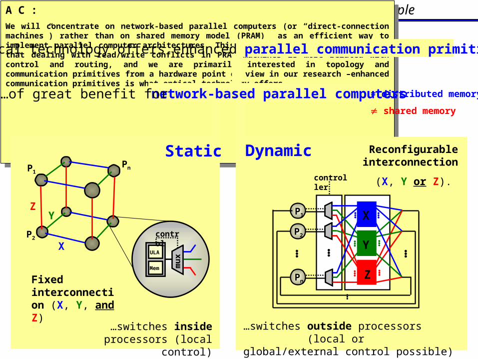
We will concentrate on network-based parallel computers (or “direct-connection machines”) rather than on shared memory model (PRAM) as an efficient way to implement parallel computer architectures. This choice is dictated by the fact that dealing with read/write conflicts in PRAM machines is more related with control and routing, and we are primarily interested in topology and communication primitives from a hardware point of view in our research –enhanced communication primitives is what optical technology offers.
A C :
We will concentrate on network-based parallel computers (or “direct-connection machines”) rather than on shared memory model (PRAM) as an efficient way to implement parallel computer architectures. This choice is dictated by the fact that dealing with read/write conflicts in PRAM machines is more related with control and routing, and we are primarily interested in topology and communication primitives from a hardware point of view in our research –enhanced communication primitives is what optical technology offers.
network-based parallel computers
Optical technology offers enhanced parallel communication primitives
Static Dynamic Reconfigurable interconnection
(X, Y or Z).
…switches inside processors (local control)
…switches outside processors (local or global/external control possible)
P1
P2
Pn
YZ
X
Fixed interconnection (X, Y, and Z)
mu
xULA
Mem
control
P1
P2
Pn
…
……
…
…
X
Y
Z
………
…
controller
…
…of great benefit for = distributed memory
shared memory

Static networks can be redesigned as single-stage dynamic networks…
I.2 Dynamic architecture vs. static
In an n-degree static topology, each processor
should have n distinct optoelectronic I/O ports…
Technologically challenging
Non reusable architecture
Bad scalability
P1
P2
Pn
…processors, switches and interconnections located in
distinct modules
Optimal use of electronic, optoelectronic and optics
Scalability, hardware reusability in other topologies
possible introduction of multiple stages…
switches interconnectionsprocessors
P1
P2
Pn
…
……
…
… ………
…
Feed-back loop
…
A C :
Actually, in our former research, we studied single-stage dynamic interconnections with global control of the switch, using spatial light modulators (OCULAR II).
A C :
Actually, in our former research, we studied single-stage dynamic interconnections with global control of the switch, using spatial light modulators (OCULAR II).

Multi-StagesSingle-Stage
S &
I -
m
…
S &
I -
2
…
S &
I -
1
P1
P2
Pn
… …
I.3 The multi-stage paradigm
architecture can be “spanned” into
The cost of multiplying the
processors is paid back as
Simplicity (switches can be elemental 2x2 cross-bars)
Scalability / Reconfigurability for different topologies
Possibility of pipelining
Theoretical background: Multi-stage architectures have been studied for decades in networking applications
Hypercube
Mesh
Cube Cycle
Shuffle/exchange
DeltaBenes
De Bruijn[computing] [computing & networking]Tree
Pyramid
Omega
Clos
Banyan
Sw
itch
&P1
P2
Pn
…
Inte
rco
nn
ect
ion
Stage mStage 1
P1
P2
Pn
P1
P2
Pn
Stage 2

connection module
…connection
module
I.2 The theoretically best optical architecture (connectivity)
MOAn(X) = A(n).I(n)… A(k).I(k)… A(1).I(1) (X)
Computation made on PE array
Optical shuffle of data between PE arrays
Optical (2D) Data flow
Processor Elements (PE)
Array
VCSEL array
Photo-detector (PD) array
PD and VCSEL flip-chip bonded
to processor array
Matrix representation of computations on
the Multistage Optical
Architecture
X
A C :
The linear architecture may be “sub-optimal” (Ozatkas) when addressing thermal dissipation issues, but offers much easier “scalability”. Also, the “flat” optimal architecture, will work well with reflective holograms, but would be much difficult to build using fiber arrays.
A C :
The linear architecture may be “sub-optimal” (Ozatkas) when addressing thermal dissipation issues, but offers much easier “scalability”. Also, the “flat” optimal architecture, will work well with reflective holograms, but would be much difficult to build using fiber arrays.

reconfigurable interconnection
module
…reconfigurable interconnection
module
reconfigurable interconnection
module
Elementary Processor Array
VCSEL arrayPhoto-detector array
SLM-based reconfigurable interconnection
Optoelectronic processing module
a) Free-Space reconfigurable interconnections
OCULAR-II
Space-invariant interconnections – good/bad?
Free-space – alignment issues?
Multi-level CGH – good diffraction efficiency
Reconfiguration (“switch”) freq. – 100 Hz…

Fixed interconnection modules...
Processor array in charge of the switching function…
OCULAR – III
Interconnection module
Interconnection module
Interconnection module
…
Elementary Processor Array
VCSEL array
Photo-detector array
Data flow
Some examples: shuffle/exchange networks, Clos and Benes crossbars, etc…
No lost of interconnection capacity if things are designed properly
b) Fixed interconnections (hybrid opto-electronic)
Indirect Binary Cube (“multistage hypercube”)
Binary Hypercube…
XY
W
Z
I.3 Two well known examples:
Self routing: “switches” are set locally by packet address (destination – input)
(Omega) network
It is full access, but not full connection.
Also useful on computing (FFT)…
0000000100100011010001010110
011110001001101010111100110111101111
Inp
ut
Ou
tpu
t
E(1) E(1) E(1) E(1)
0000000100100011010001010110
011110001001101010111100110111101111
(4)(4) (4)(4)
feed-back
(2) (3) (4) E(1)E(1)E(1)E(1)
-1(4)P0
=
A C :
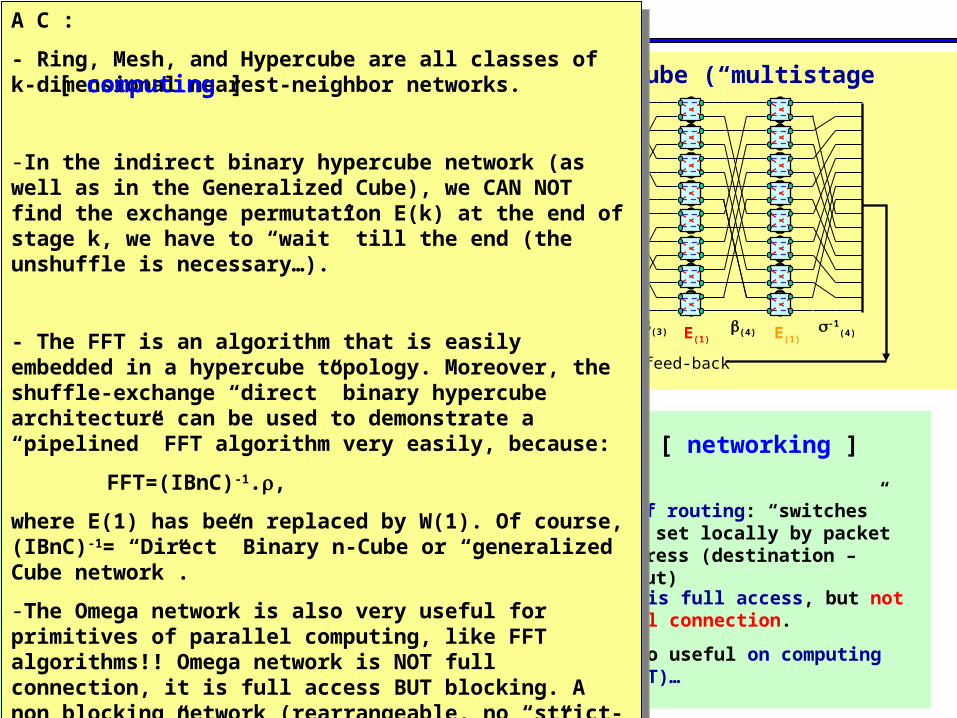
- Ring, Mesh, and Hypercube are all classes of k-dimensional nearest-neighbor networks.
-In the indirect binary hypercube network (as well as in the Generalized Cube), we CAN NOT find the exchange permutation E(k) at the end of stage k, we have to “wait” till the end (the unshuffle is necessary…).
- The FFT is an algorithm that is easily embedded in a hypercube topology. Moreover, the shuffle-exchange “direct” binary hypercube architecture can be used to demonstrate a “pipelined” FFT algorithm very easily, because:
FFT=(IBnC)-1.,
where E(1) has been replaced by W(1). Of course, (IBnC)-1= “Direct” Binary n-Cube or “generalized Cube network”.
-The Omega network is also very useful for primitives of parallel computing, like FFT algorithms!! Omega network is NOT full connection, it is full access BUT blocking. A non blocking network (rearrangeable, no “strict-non blocking” nor “wide sense non-blocking”) is the BENES network. CLOS is another which is strict-non blocking (but the network is not constructed using 2x2 cross-bar switches).
-Other interesting architecture would be the Batcher-Banyan, which is “wide-sense” non-blocking… In fact, the OMEGA and IBnC demonstrated here are EQUIVALENT networks (so here the examples are not the best ones)
REM: for OC2002, build the hypercube using the exchange, so that pipelining the quad-three compression becomes possible. Then, build other multi-stages.
A C :
- Ring, Mesh, and Hypercube are all classes of k-dimensional nearest-neighbor networks.
-In the indirect binary hypercube network (as well as in the Generalized Cube), we CAN NOT find the exchange permutation E(k) at the end of stage k, we have to “wait” till the end (the unshuffle is necessary…).
- The FFT is an algorithm that is easily embedded in a hypercube topology. Moreover, the shuffle-exchange “direct” binary hypercube architecture can be used to demonstrate a “pipelined” FFT algorithm very easily, because:
FFT=(IBnC)-1.,
where E(1) has been replaced by W(1). Of course, (IBnC)-1= “Direct” Binary n-Cube or “generalized Cube network”.
-The Omega network is also very useful for primitives of parallel computing, like FFT algorithms!! Omega network is NOT full connection, it is full access BUT blocking. A non blocking network (rearrangeable, no “strict-non blocking” nor “wide sense non-blocking”) is the BENES network. CLOS is another which is strict-non blocking (but the network is not constructed using 2x2 cross-bar switches).
-Other interesting architecture would be the Batcher-Banyan, which is “wide-sense” non-blocking… In fact, the OMEGA and IBnC demonstrated here are EQUIVALENT networks (so here the examples are not the best ones)
REM: for OC2002, build the hypercube using the exchange, so that pipelining the quad-three compression becomes possible. Then, build other multi-stages.
[ computing ]
[ networking ]

…an optical “3D optical wiring” module between 2D VLSI arrays.
II. Optical fiber-based plane-to-plane interconnection modules
input output
Fiber module
(2)

II.1 Fiber-based interconnection blocks for multistage architectures.
• Inter-stage connection fixed and point-to-point: channels can be fibers.
• Fibers have better efficiency and just like free-space optics, no cross-talk in 3D.
• No space-invariance required.
• Precise and robust alignment possible.
• Theoretically more volume efficient than free-space equivalent!
• Maybe “hard” to build? Boring, but not a fundamentally difficult - can be automated…
• Alignment of both output and input needed…
• Power dissipation may be a fundamental limitation, but we are far from these limits…
input output
Prototype Fiber module (fibers and holders)
“integrated” 2D folded
perfect shuffle permutation
module
(2)
…wave-guide arrays for fixed, point-to-point and space variant interconnections are an interesting alternative to free-space optics
“Volume-consumption comparisons of free-space and guided-wave optical interconnections”, Y.Li and J. Popelek, p.1815-1825, Appl.Opt. Vol 39, n.11, april 2000.

II.2 “Decomposition” of the interconnect into modules
Many multistage networks use simple, regular interconnections…
[ Problem ]
A C :
In group-theoretic-based construction of MINs (giving symmetric networks), the most useful permutations are the exchange, the shuffle, the butterfly, the bit reversal and the shift permutation.
The nature of the decomposition of the interconnect into EITHER the column, row or the diagonal dimensions may also reintroduce the use of light-efficient one dimensional, non pixilated, rapid reconfigurable diffractive elements (such as acousto optics).
However, when folded in a plane, these may materialize as non-regular, non-scalable and non-reusable interconnection modules!
0
1
2
3
4
5
6
7
8
9
10
11
12
13
14
15
0
1
4
5
2
3
6
7
8
9
12
13
10
11
14
15
columns
row
s
Scan map Fractal map

Permutations are decomposed “ad-hoc” into their “row” and “column” exclusive permutations
parts, plus some simple-to-fold “link” permutation…
Because it may be possible to cascade fiber-based modules without too much loss of light power, let’s “break” these into simple to fold modules.
[Solution ]
“simple to fold” means:
1) Simple to implement by stacking planer wave-guide structures
2) Or simple to implement using previously built modules (scalability)
Permutations are decomposed “recursively”
vertical horizontal diagonal

The idea is to define permutation “constructors” that correspond to basic building steps using PLC circuits (stacking, grouping modules).
This decomposition methodology also applies to the switching stages (no other thing that a set of possible permutations)
Z Pn
“zoom” constructor
Q Pn
“quadrant” constructor
Ln/2 Pn/2 Rn/2 Pn/2
Permutation layer Pn/2
Permutation module Pn
Vertical replicator
Horizontal replicator

Let’s try that on the previous examples:
Indirect Binary n-Cube Network
(Omega) network
…uses the butterfly (k)
and perfect shuffle (k) permutations
…uses only the perfect shuffle (k) permutation
feed-back
(2)(3) (4) E(1)E(1)E(1)E(1)
-1(4)P0=
0000000100100011010001010110011110001001101010111100110111101111
Inp
ut
Ou
tpu
t
E(1) E(1) E(1) E(1)
0000000100100011010001010110011110001001101010111100110111101111
(4)(4) (4)(4)

Example: shuffle and butterfly decomposition
…It is easy to see that the ad-hoc folding of a “regular” permutation
needs a maximum of three concatenated “stacked” modules
{bn, … bk+1, bk, bk-1, … b2, b1}
shuffle n(k)
{bn, … bk+1, bk-1, bk-2, … b1, bk}
butterfly n(k)
n(k)
n(k)
{bn, … bk+1, bk, bk-1, … b2, b1}
{bn, … bk+1, b1, bk-1, … b2,bk}
n(k) = Ln/2 n/2; Rn/2 n/2 ; L
Decomposition using constructors:
= ; ;= ; ;
n(k) = Rn/2 n Ln/2 n/2; n/2 ; L
“ad-hoc”
“ad-hoc”
“recursive”
2p(2p) = Qp-1 T2 (1,2)

(k)= row(k)
Folding the shuffle permutation
(k) = row(n/2) .col(k-n/2).L
- and L is the “link” permutation.
col(2)
If k n/2, the shuffle “acts” over rows :
- where col is a column shuffle,
row(k)
If k > n/2, the shuffle can be written as:
Link0
1=001
2
3
4=100812
input plane
0
1
2
3
4
5
6
8
0
1
2
3
4
5
6
8
0
1
2
3
0
1
2
3
4
5
6
8
output plane
Can be built by stacking “slices”

(2) = row(2)
Folding a butterfly into a 4x4 array
(k)= col (k-n/2).L.col(k-n/2)
- and L exchanges row and column LSB
Link0
1=001
2
3
4=100812
col(2)
If k n/2, the butterfly (k) “acts” over rows :
- where col is a column butterfly,
row(2)
If k > n/2, the butterfly (k) can be written as:
A C :
REM: the modules can be built by stacking layers, to that planar-optics technology used. In particular, we can think again about fan-in and fan-out channels… (cf. NHK company.
A C :
REM: the modules can be built by stacking layers, to that planar-optics technology used. In particular, we can think again about fan-in and fan-out channels… (cf. NHK company.
input plane
0
1
2
3
4
5
6
8
output plane
input plane
0
1
2
3
4
5
6
8
0
1
2
3
4
5
6
8
0
1
2
3
0
1
2
3
4
5
6
8
output plane

…back to examples: network
shuffle shuffle shuffleshuffle
Processor arrays
(exchange switches and more)
row(2
L
90º
col(2
pair of PE implement elemental exchange switch

I.3 Indirect Binary 4-Cube
(2) (3)
PE array 1(exchange)
PE array 2(exchange)
PE array 3(exchange)
(4)
PE array 4(exchange)
-1(4)
Processor arrays
(exchange switches and more)

III. 4x4 prototype fiber module. Preliminary tests
Two holder prototypes: Zirconium, SiO2
Pitch: 250±5 mMultimode graded index fibers: NA=0,21
(core 50m, cladding 126m)Transmission loss: 3dB/km
Length: 30 cm

Input (VCSEL
854±4nm)Output (CCD)
III.1 Preliminary tests on a 4x4 prototype module
[ Interconnection pattern ] [ Transmittance (one channel) ]
Max. transmittance 38,45% for I=9,5 mA
0
5
10
15
20
25
30
35
40
45
6 7 8 9 10 11 12 13
VCSEL driving current (mA)
Tra
nsm
itta
nce
(%
)
38,45
9,5
LED regime
LASER regime
(2)
A C :
REM: the light coming from the non-addressed channels is mainly due to some default functioning of the neighboring VCSELs which emits LED light though they are OFF!
A C :
REM: the light coming from the non-addressed channels is mainly due to some default functioning of the neighboring VCSELs which emits LED light though they are OFF!

(2)input output
No relay optics between
VCSEL array and fiber
module input
III.2 Alignment tolerances (test performed on a single channel)
x 50 m
VCSEL array
X,Y, and Z translation stage
Power meter
VCSEL ON
Horizontal excursion
0
0.05
0.1
0.15
0.2
0.25
-105 -90 -75 -60 -45 -30 -15 0 15 30 45 60 75
X (microns)
exit
po
wer
(m
W)
x
Alignment tolerances
(half peak power)
y 70 m
A C :
The differences on alignment tolerances are probably due to the non-circular shape of the VCSEL mode.
A C :
The differences on alignment tolerances are probably due to the non-circular shape of the VCSEL mode.

IV. Conclusion
Input/output alignment of modules
• Microlenses, Fibers with round ends.
• Modules built from fiber bundles.
• Active alignment.
Demonstrator architectures using smart pixel arrays (2x2 or 4x4 electronic switches)
[ Present research ]
A C :
Multi-function modules: the use of optical fiber modules fits well with the all optical approach; for instance, one can imagine a module with several different interconnection patterns, but also other “optical-functions” like optical delay lines:
However, in all-optical networks the “switches” may be very fast (electro optical devices, not MEMS), because the delay time for avoiding the drop of ATM cells is ?? for a typical Gigabit network!!!
0
1
2
3
Optical interconnection

[ Future research directions ]
Multi-interconnection modules
• “Mixed” interconnections, and other optical functions
• Circuit switching for all optical networks
• Packet switching in a buffered architecture with globally controlled stages
Integrated plane-to-plane multistage paradigm
• using permutation “slices” for intra-chip massive, regular interconnections.
Guided-wave interconnects can be “modulated” and integrated !
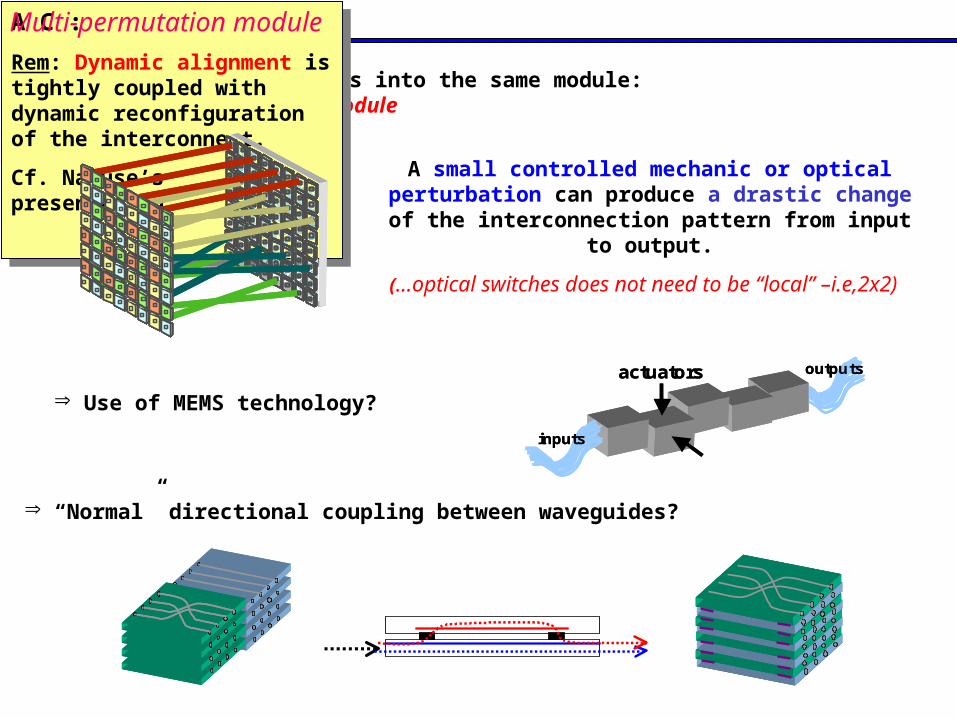
Interleaved permutations into the same module: multi-permutation/switch module
A C :
Rem: Dynamic alignment is tightly coupled with dynamic reconfiguration of the interconnect.
Cf. Naruse’s presentation.
A C :
Rem: Dynamic alignment is tightly coupled with dynamic reconfiguration of the interconnect.
Cf. Naruse’s presentation.
“Normal” directional coupling between waveguides?
Multi-permutation module
A small controlled mechanic or optical perturbation can produce a drastic change of the interconnection
pattern from input to output.
(…optical switches does not need to be “local” –i.e,2x2)
actuators
inputs
outputsactuators
inputs
outputs
Use of MEMS technology?

Transparent circuit switching by TDM interconnections
We are now building a demonstrator using mechanical displacement of modules containing a by-pass interconnection and cube interconnections
control
{ (1) , i}
bi-module
{ (2), i}
bi-module
{ (3), i}
bi-modulePE
arr
ay
control
{ (1) , i}
bi-module
{ (2), i}
bi-module
{ (3), i}
bi-modulePE
arr
ay
{ (1) , i}
bi-module
{ (1) , i}
bi-module
{ (2), i}
bi-module
{ (2), i}
bi-module
{ (3), i}
bi-module
{ (3), i}
bi-modulePE
arr
ay
“spanned” hypercube with weak-communication
“all-optical” multistage architecture
…optical switches does not need to be “local” (2x2)

…globally controlled exchange stages + Intermediate buffers
A new paradigm for packet switching in multistage networks
{(1) , i}
bi-module
{(2), i}
bi-module
{(3), i}
bi-module
module control module control module control
PE
arr
ay
PE
arr
ay
PE
arr
ay
inp
ut
out
put
{(1) , i}
bi-module
{(1) , i}
bi-module
{(2), i}
bi-module
{(3), i}
bi-module
{(3), i}
bi-module
module control module control module control
PE
arr
ay
PE
arr
ay
PE
arr
ay
inp
ut
out
put
0 0.1 0.2 0.3 0.4 0.5 0.6 0.7 0.8 0.9 10
0.1
0.2
0.3
0.4
0.5
0.6
0.7
0.8
0.9
1Selection method: alternate / Backpressure: on / mode: disablehop
Input request probability (per unit time)
No
rma
lize
d T
hro
ug
hp
ut (
ba
nd
wid
th)
0
0
1
Length of buffers1
Length of buffers
2
Length of buffers
2
Length of buffers
3
Length of buffers
3
Length of buffers
4
Length of buffers
4
Length of buffers
64x64 Crossbar64x64 MIN64x64 GS-MIN
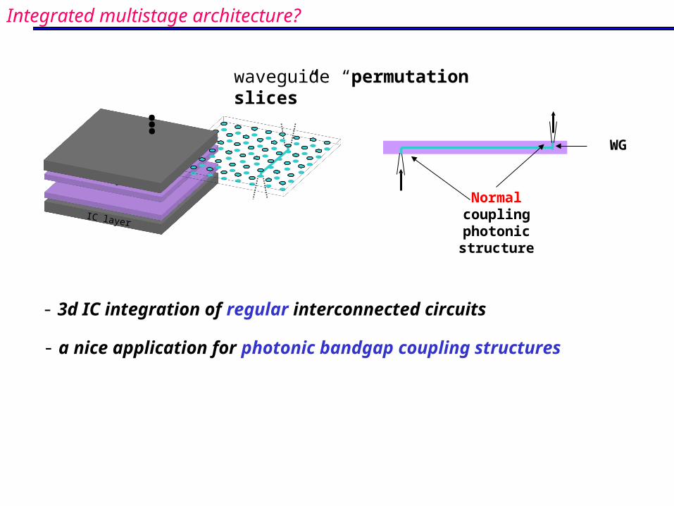
waveguide “permutation slices”
IC layer
IC layer
…
- a nice application for photonic bandgap coupling structures
- 3d IC integration of regular interconnected circuits
Integrated multistage architecture?
WG
Normal coupling photonic structure