a dpll-based per core variable frequency clock...
TRANSCRIPT
Symposia on VLSI Technology and Circuits
A DPLL-based per Core Variable
Frequency Clock Generator for an
Eight-Core POWER7™ Microprocessor
José Tierno1, A. Rylyakov1, D. Friedman1, A. Chen2, A. Ciesla2, T. Diemoz2, G. English2, D. Hui2, K. Jenkins1, P. Muench2, G. Rao2, G. Smith2, M. Sperling2, K. Stawiasz1
1 IBM Thomas J. Watson Research Center2 IBM Systems and Technology

Slide 1
Outline
• POWER7 Architecture
• DPLL Design
• DPLL Measurements
• Conclusions / Acknowledgements
Slide 1
Slide 2
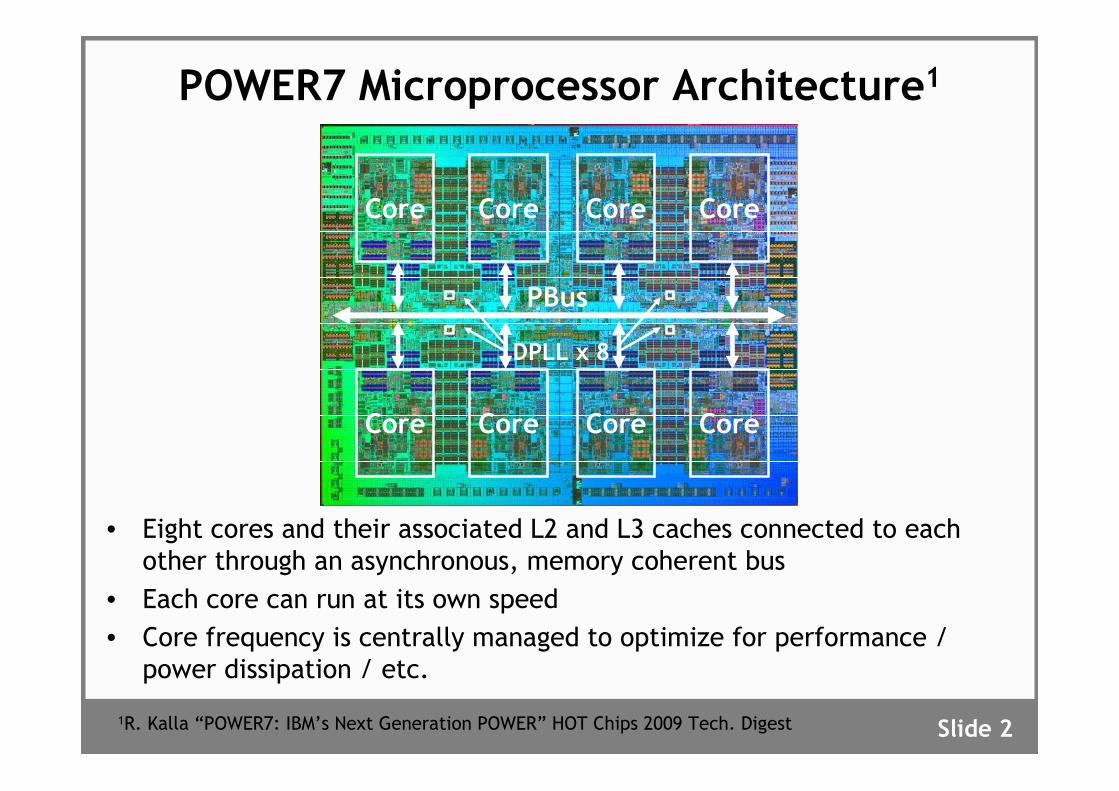
POWER7 Microprocessor Architecture1
• Eight cores and their associated L2 and L3 caches connected to each other through an asynchronous, memory coherent bus
• Each core can run at its own speed
• Core frequency is centrally managed to optimize for performance / power dissipation / etc.
Core Core Core Core
Core Core Core Core
DPLL x 8
PBus
Core Core Core Core
Core Core Core Core
DPLL x 8
PBus
1R. Kalla “POWER7: IBM’s Next Generation POWER” HOT Chips 2009 Tech. Digest

Slide 3
Detail of POWER7 Micrograph: One Core
DPLL
Core
L2 C
ache
L3 Cache + Interconnect
5.5
mm
10 mm
350 µm x 200 µm

Slide 4
Microprocessor Frequency Control
• The power manager takes input from environmental sensors, performance counters, and software requests, and continuously adjusts the frequencies of each core
• All is done transparently with respect to code execution
Power Manager
Environmental Sensors
Performance Counters
OS/Software Requests
DPLLDPLLDPLLDPLL
Freq1
Freq2
Freq3
FreqN
Clocks to
Cores

Slide 5
Microprocessor Frequency Management
• Effective power / frequency management requires frequency changes without interrupting code execution
– Large, uninterrupted frequency range (100’s of MHz to multiple GHz) necessary to go from low frequency idling modes to high frequency turbo modes
– Smooth frequency transitions without any missing clock cycles to avoid power supply drops caused by di/dt and other transients in the clock distribution network
– No undershoots in cycle time, under any circumstances
– Support for frequency spreading

Slide 6
DPLL Fits the Bill Nicely
• Lower area than an APLL: We want at least one PLL per core, for independent frequency control
• Overall push to reduce the amount of analog contents in the processor
• DPLL uses same digital methodology (verification, timing analysis, manufacturing test) as the rest of the microprocessor

Slide 7
DPLL Architecture2
PFD PI Loop Filter Feed-
Forward∆Σ
DCO Control
DCO
Programmable Voltage Regulator
Frac-N ∆Σ
Multiplier Filter
2/4/8 Pre-
scaler
Multi-modulus Feed-back
Divider
1/2/4 Output Divider
Row
Col
24
16
3
Dither
Integer Control
8
Fract. Control
9
Early/Late
Fast/Slow2
2
Proportional Bypass
Fractional Multiplier
10
Integer Multiplier
6
Clock-gating signals3
Feedback clock, to all digital logic
Output Clock
Reference Clock
Slew-rate
Multiplier
8
8
2J.A. Tierno et al “A Wide Power Supply Range, Wide Tuning Range, All Static CMOS All Digital PLL in 65 nm SOI” IEEE JSSC, Vol. 43, Issue 1, pp. 42-51, Jan. 2008
New Components

Slide 8
Three-stage Digitally Controlled Ring
Oscillator: Wide Dynamic Range
• Output frequency a function of the fraction of enabled inverters
• Dynamic range: From 800 MHz to 15 GHz
• Voltage regulator guarantees good jitter performance
0 1 2
0 1 2
0 1 2
0 1 2
0 1 2
Some inverters are turned on
Some inverters are turned off
Phase 0Phase 1Phase 2

Slide 9
DCO Voltage Regulator
• The DCO uses an on-chip programmable voltage regulator
– Insulates the ring oscillator from the noisy power supply, greatly reducing the jitter of the RO
– Allows centering the range of the ring oscillator across process corners
• The DCO voltage regulator is the only analog component in the DPLL

Slide 10
Bang-bang Self-timed PFD
Ref Clk
FB Clk
Mutex
C
Reset
FB Early
Ref Early
Ref Edge
Ref First
FB First
FB Clk
Ref Faster
FB Faster
FB Edge
R
R
Ref Clk
A
B
A first
B first
W

Slide 11
Frequency-proportional Output of the PFD
• A pulse is generated in Ref Faster every time that Ref Clk gains one full cycle w.r.t. FB Clk
• The pulse rate in Ref Faster is the difference in frequencies between Ref Clk and FB Clk
• This pulse is used by the loop filter to quickly sweep in frequency while the PLL is out of lock
• When the PLL is in lock, neither Ref Faster nor FB Faster generate any pulses
Ref Clk
FB Clk
Ref Edge
Ref Faster

Slide 12
Loop Filter with Frequency Ramp Tracking
• During frequency acquisition, Ref Faster and FB Faster are active, and quickly drive DCO Control close to its final value (k_freq >> k_int)
• During phase acquisition, Ref Faster and FB Faster are inactive,and the loop filter dynamics are set by k_int and k_prop
x k_int
x k_freq
x k_freq
++ -
+
x k_prop
Ref Early
Ref Faster
FB FasterFB Clk
DCO Control

Slide 13
Slew-rate Controlled Frequency Ramp
• This DPLL is part of the power management infrastructure in POWER7, and can be used to change the frequency of operation of each core independently, and without stopping code execution
– While changing frequency, no short cycles should be generated
– No overshoot in frequency (undershoot in cycle time) can ever happen
– Constant df/dt insures constant di/dt on the power supply

Slide 14
Frequency Filter / Ramp Generator
• Frequency filter generates a ramp of multipliers by incrementing / decrementing the multiplier at a steady rate
• Multiplier slew-rate is controlled by changing the rate of a divided clock
Mult_acc
14Mult_in
Mult_slew
%N
DPLL Clk
Mult_outto Frac-N ∆Σ
14
8
Clock Divider
Shift and Pad
14
0
1
Filter Bypass
10
14
a
b
a>b
a<bComp
dec
inc

Slide 15
POWER7 DPLL Testing
• Test fixture used for electrical characterization of POWER7 DPLL. The aluminum cooling plunger and blue cooling lines supply refrigerated water to cool the chip package

Slide 16
140 MHz/uS 70 MHz/uS
17.5 MHz/uS
Frequency Ramp
1.50
2.00
2.50
3.00
3.50
4.00
4.50
-30.00 20.00 70.00 120.00 170.00
Time (uS)
Fre
qu
ency
(G
Hz)
Measured Frequency: Slew-rate Controlled
Frequency Ramp

Slide 17
Measured Cycle-time: End-of-ramp Transient
0.248
0.25
0.252
0.254
0.256
0.258
0.26
25.00 30.00 35.00 40.00 45.00 50.00
Time (us)
Tcy
cle
(ns)
Frequency Acquisition
Phase Acquisition
Lock
DCO Tcycle Step (~ 2 ps)
17.5 MHz/us

Slide 18
Spread Spectrum Tracking
• Spreading: +/- 2.5% @ 50 kHz
• Output Frequency: 4 GHz
• DPLL tracks without losing lock

Slide 19
Measurements Summary
Digital Logic + DCO200 µm x 175 µm
CommentsValueParameter
200 MHz reference140 MHz/µs to 600 kHz/µs Frequency Slew-Rate
DCO running at 10 GHz, 200 MHz reference
30 mA @ 5 GHzPower
Voltage regulator200 µm x 175 µmArea
200 MHz reference100 ps pk-pk @ 4 GHzLong Term Jitter
200 MHz reference1 ps RMS @ 4 GHzPeriod Jitter
Output frequency is divided by two
Continuous 800 MHz to 15 GHz achievable over PVT
Tuning Range

Slide 20
Conclusions / Acknowledgements
• We designed a compact, efficient all-digital PLL in 45 nm SOI, used to set per-core frequency in an 8-core POWER7 microprocessor
• The PLL can be used to change the operating frequency of the core while instructions are executing
• A specially designed PFD provides extra outputs that are used by the loop filter to track a fast frequency ramp without making the system unstable
Acknowledgments: This material is based upon work supported by the Defense Advanced Research Projects Agency under its Agreement No. HR0011-07-9-0002

Slide 21
Backup Slides

Slide 22
Bang-bang PFD Timing Diagram
• Bang-bang PFD detects arrival order and keeps it stable for one reference or divided clock cycle
• Output is re-sampled with a delayed version of FB_Clk before being used in loop filter
Ref Clk
FB Clk
Ref Edge
FB Edge
Reset
Ref First

Slide 23
DPLL Clocking
• To ease data transfer timing constraints, clocks in the DPLL digital logic are derived from the pre-scaled DCO output
• Multiple phases/frequencies are obtained by using enables to select one edge out of many
Phase HoldGrid Clock
Qualified Grid Clock
Clock Pre-scaler
Div 1/2/4 0
1
DCO output
Reference Clock
Clock Bypass
Clock Distribution to all internal logic
Phase Holds
Grid Clock

Slide 24
Measured Period Jitter
• Sub-ps RMS period jitter at the high end of the scale• Very few inverters enabled at the low end of the scale; period jitter increases accordingly
0 1000 2000 3000 4000 5000 6000 70000
5
10
15
20
25
Per
iod
Jit
ter
RM
S (
ps)
Clock Frequency ( MHz )