a differential hall effect measurement method with sub
TRANSCRIPT
1926
A differential Hall effect measurement method withsub-nanometre resolution for active dopant concentrationprofiling in ultrathin doped Si1−xGex and Si layersRichard Daubriac*1, Emmanuel Scheid1, Hiba Rizk1, Richard Monflier1, Sylvain Joblot2,Rémi Beneyton2, Pablo Acosta Alba3, Sébastien Kerdilès3 and Filadelfo Cristiano1
Full Research Paper Open Access
Address:1LAAS-CNRS and Univ. of Toulouse, 2STMicroelectronics, 850 rueJean Monnet, 38926 Crolles, France and 3CEA-LETI and Univ. ofGrenoble, 17 rue des Martyrs, 38054 Grenoble, France
Email:Richard Daubriac* - [email protected]
* Corresponding author
Keywords:carrier mobility; contact resistance; differential Hall effect; dopantactivation; fully depleted silicon on insulator (FDSOI); laser annealing;sub-nanometre resolution
Beilstein J. Nanotechnol. 2018, 9, 1926–1939.doi:10.3762/bjnano.9.184
Received: 08 March 2018Accepted: 07 June 2018Published: 05 July 2018
This article is part of the Thematic Series "Metrology and technologycomputer aided design for the sub-10 nm technology node".
Guest Editor: P. Eyben
© 2018 Daubriac et al.; licensee Beilstein-Institut.License and terms: see end of document.
AbstractIn this paper, we present an enhanced differential Hall effect measurement method (DHE) for ultrathin Si and SiGe layers for the
investigation of dopant activation in the surface region with sub-nanometre resolution. In the case of SiGe, which constitutes the
most challenging process, we show the reliability of the SC1 chemical solution (NH4OH/H2O2/H2O) with its slow etch rate, stoi-
chiometry conservation and low roughness generation. The reliability of a complete DHE procedure, with an etching step as small
as 0.5 nm, is demonstrated on a dedicated 20 nm thick SiGe test structure fabricated by CVD and uniformly doped in situ during
growth. The developed method is finally applied to the investigation of dopant activation achieved by advanced annealing methods
(including millisecond and nanosecond laser annealing) in two material systems: 6 nm thick SiGeOI and 11 nm thick SOI. In both
cases, DHE is shown to be a uniquely sensitive characterisation technique for a detailed investigation of dopant activation in ultra-
shallow layers, providing sub-nanometre resolution for both dopant concentration and carrier mobility depth profiles.
1926
IntroductionThe research efforts made throughout the last decades have
made it possible to keep the momentum for a continuous minia-
turization of electronics devices. For instance, the “bulk” planar
transistor limitations have been overcome thanks to the transi-
tion towards more complex device architectures. These include
enhanced planar architectures such as fully depleted silicon on
insulator (FDSOI) [1] or 3D architectures ranging from TriGate
FinFETs [2] to gate-all-around NWFETs [3] and monolithic 3D
CoolCube technology [4]. Despite their differences, some tech-
nological issues have emerged as a significant challenge for all
Beilstein J. Nanotechnol. 2018, 9, 1926–1939.
1927
of them, such as the need to reduce the contact resistance at the
silicide/source–drain interface [5].
The increase of the active dopant concentration at the surface of
the source/drain material (usually Si or SiGe) is a key factor for
obtaining a resistance reduction [6], and several process solu-
tions have been proposed to this purpose, involving advanced
implanting or annealing techniques [7]. Within this context, the
optimization of existing characterisation techniques for the
measurement of dopant activation at the semiconductor
surface (or the development of new ones) is therefore decisive
for both the improvement of the fabrication processes and the
calibration of the related technology CAD (TCAD) physical
models.
For device architectures based on planar SOI substrates (such as
FDSOI or 3D CoolCube), measurements of active dopant con-
centrations from “blanket wafer” experiments are still relevant
for process and TCAD optimisation, which are in principle
achievable thanks to several known 1D measurement tech-
niques previously developed for dopant profiling. However, in
the case of contact resistance optimisation, only the dopant con-
centration close to the surface is relevant, i.e., within the first
few nanometres, while the SOI/SiGeOI substrates used in cur-
rent technologies are extremely thin (top layer < 10 nm),
making measurement techniques with sub-nanometre resolu-
tion necessary. 1D techniques based on small-angle bevel prep-
aration (such as spreading resistance profiling (SRP) [8] or
scanning capacitance microscopy (SCM) [9,10]) become
extremely difficult to implement and control in view of such a
small resolution. Thanks to the use of an AFM tip, 2D scanning
spreading resistance microscopy (SSRM) has been shown to
achieve sub-nanometre resolution [11,12]. However, in this
technique, the carrier concentration is inferred from a resis-
tivity profile under the assumption that carrier concentration
varies ideally with mobility, which is not always the case, espe-
cially when a part of the dopant is not electrically active [13].
For this reason, reliable mobility and concentration profiling
based on scanning probe techniques require a combination of
resistivity measurements by SSRM with carrier concentration
measurements by SCM [14]. Finally, capacitance-based tech-
niques such as SCM or electrochemical capacitance voltage
(ECV) [15], provide reliable values of carrier concentrations
only in the absence of additional electrically active defects,
which can affect the CV signal [16].
In contrast, differential Hall effect (DHE) profiling [17,18] can
potentially meet all the requirements related to the precise mea-
surement of dopant activation at the semiconductor surface.
DHE relies on the iteration of etching process and conventional
Hall effect measurements. The active carrier profile is therefore
measured without any assumption about the magnitude of the
carrier mobility. In addition, measurements are made by strip-
ping the material in successive steps rather than bevelling the
surface. The depth resolution of the final dopant concentration
profile is therefore defined by the etch rate and indeed nano-
metric resolution has been successfully demonstrated for Si and
Ge, applying oxidation processes such as anodisation [19] or
oxidising chemistry [20-23]. Nevertheless, etching SiGe alloys
with nanometric resolution is far more challenging considering
that Si and Ge have different oxidation rates [24]. For this
reason, reliable DHE measurements of doped SiGe layers have
not been reported in literature. Finally, in all published DHE in-
vestigations, the removal rate is assumed to stay constant. How-
ever, even small variations in the removed thickness among
nominally identical etch steps can strongly distort the final
carrier concentration and mobility profiles.
In this paper, we present an enhanced differential Hall effect
measurement method that allows to precisely determine the
level of dopant activation close to the semiconductor surface for
Si and SiGe. First, we detail the etching processes that we have
developed for each semiconductor, with particular focus to the
SiGe case, which constitutes the most challenging process. For
both materials, our method includes a direct measurement of the
removed thickness after each removal step, so to avoid aver-
aging the etch rate and improve the accuracy of final calculated
values. Then, we demonstrate the reliability of a complete DHE
procedure on a dedicated SiGe test structure fabricated by CVD
and uniformly doped in situ during growth. Finally, we will
apply our DHE method to the investigation of dopant activation
achieved by advanced annealing methods in two material
systems: 6 nm SiGeOI and 11 nm SOI.
Development of Etching Processes forSi1−xGex and SiEtching process for Si1−xGexDifferent methods have been proposed in literature for the con-
trolled etch of SiGe layers [25-27]. We first analysed the main
characteristics of each solution in terms of the specific require-
ments related to their application for DHE measurements. In
particular, (i) the solution must etch Si and SiGe simultaneous-
ly so that the SiGe stoichiometry is not modified; (ii) the solu-
tion must be strongly selective with respect to Si so to preserve
the surrounding Si areas in Van der Pauw test structures;
(iii) the solution must be chemically active for a relatively
long period (about 1 day) so to be used for several “etch and
measurement” cycles; (iv) the etch rate must be slow
(ca. 1 Å·min−1) to allow for sub-nanometre resolution. Taking
into account the above mentioned criteria, we therefore selected
the one-step chemistry based on SC1 (NH4OH/H2O2/H2O
Beilstein J. Nanotechnol. 2018, 9, 1926–1939.
1928
1:1:5), which oxidizes and removes both materials at the same
time.
We then investigated the efficiency of the SC1 solution by
running several tests as a function of different experimental pa-
rameters including time, temperature and Ge content. For this,
spectroscopic ellipsometry (with a HORIBA Jobin Yvon
system) was used as a fast, reliable and non-destructive method
for the measurement of the removed thickness. We developed
an empirical model for the quantification of the SiGe thickness
measurement (based on a SiGe/Si two layers stack and a point-
by-point calculation procedure), which was calibrated using
other techniques (such as TEM and XRD). As an example,
Figure 1 summarizes the removed thickness measured by XRD
(in (004) configuration), high-resolution TEM and ellipsometry
as a function of the etching time of a 20 nm thick Si0.73Ge0.27
boron-doped layer (1018 cm−3) grown on top of a Si substrate.
Figure 1: Removed SiGe thickness measured by different methods(TEM, XRD and ellipsometry) as a function of the etching time. Gecontent: 27 atom %. Inset: TEM cross-section micrographs of refer-ence and the sample etched for 30 min. This figure illustrates theagreement between the three chosen techniques.
TEM images show a clear decrease of the layer thickness, while
all the techniques are in mutual agreement, therefore validating
ellipsometry as a unique thickness characterization method for
the remainder of this work. From this study we estimated a
value of 0.95 Å·min−1 for the etch rate of the SC1 solution on
Si0.73Ge0.27, without any alteration of the initial layer stoichi-
ometry, as confirmed by XRD analysis (Figure S1, Supporting
Information File 1). Moreover, the found etch rate is in very
good agreement with previous results obtained by our research
group [26]. Concerning the surface roughness, tapping mode
AFM analysis provided arithmetic averages Ra of about 1.2 Å
(Figure S2, Supporting Information File 1).
However, in view of its application for DHE experiments, it is
necessary to use an encapsulation cell to protect metallic
contacts of the electric test structures during etch (Figure S3,
Supporting Information File 1). Due to the funnel-shaped cell
designed for this study, the reaction zone is confined, which
results in a reduction of the etch rate. By optimising the experi-
mental set up (use of a magnetic stirrer combined with an
appropriate cell orientation in the solution bath), we managed to
limit the etch rate reduction and similar values to experiments
with “blanket” samples were found. Finally, we investigated the
impact of the Ge content on the measured etch rate. The results
are shown in Figure 2, where we compare the removed thick-
ness as a function of the etching time for two 20 nm boron-
doped (1019 cm−3) Si1−xGex samples with different germanium
content : x = 0.22 and x = 0.30. For etching times less than
15 min, the etch rate is perfectly linear and independent of the
Ge content, with a removed thickness of ca. 1 nm after 15 min.
It is therefore possible to use this solution to achieve sub-
nanometre resolution. In summary, all these investigations
confirm the choice of SC1 as chemical solution for SiGe
etching because of its slow etch rate, stoichiometry conserva-
tion and low roughness generation.
Figure 2: Removed SiGe thickness (measured by ellipsometry) as afunction of etching time for two different Ge contents. After the first15 min, the etch rate increases with Ge content.
Etching process for SiThe silicon etching process differs from the etching of SiGe
insofar as it involves a two-step mechanism: first, oxidation and
then oxide stripping. In this case, the etch rate is not defined as
a function of the etching time, but is given by the removed
thickness per step, i.e., the removed thickness between two
stripping processes. A resolution of about 1 nm has been ob-
tained in the study of Ling et al. [22] combining dilute HF,
ultrapure water rinsing and re-oxidation in a clean-room envi-
ronment. However, with the aim of minimising the surface
roughness, we used ethanol instead of ultrapure water as rinsing

Beilstein J. Nanotechnol. 2018, 9, 1926–1939.
1929
solvent [28]. We performed multiple cycles of etching pro-
cesses on in situ boron-doped Si layers (grown on top of Si sub-
strates) with continuous monitoring of the removed thickness
(by ellipsometry measurements) and the surface roughness (by
AFM characterization). Our results show a cycle-by-cycle etch
rate below 1 nm and a final roughness of 1 Å.
DHE procedure validation on SiGe layersfabricated by CVDIn this section, we detail a complete DHE procedure using a
20 nm thick boron-doped (1019 cm−3) Si0.77Ge0.23 layer grown
by CVD on top of a Si substrate. We first describe the Van der
Pauw structure and the conventional Hall effect setup. Then we
will present the differential Hall effect measurements and calcu-
lations and we will discuss the limitations of the technique.
Van der Pauw structure and Hall effectmeasurements on ultrathin layersThe Hall effect measurement is a well-known technique that
allows one to access three important physical parameters for
material characterization: the sheet resistance Rs, the active Hall
dose NH and the Hall mobility µH. At first, a Van der Pauw
technique is used to determine the sheet resistance, then a mag-
netic field is applied orthogonally to the sample surface to
measure the sheet Hall coefficient RSH, which is finally used to
deduce NH and µH.
Several classical Van der Pauw shapes were tested to perform
electrical measurements (square, Greek cross and bridge “bar-
shaped” structures). A test structure in the form of a Greek cross
has been chosen as it has more advantages than other shapes
(Figure S4, Supporting Information File 1). First, it provides an
error of less than 1% on both sheet resistance and Hall coeffi-
cient measurements [29-32]. Moreover, it has a highly symmet-
rical shape with peripheral contacts separated from the centre
region, in which the current lines converge allowing
precise characterization. For this last reason, we were able to
design an encapsulation cell (Figure S3, Supporting Informa-
tion File 1) defining a reaction region in the centre part of the
Greek-cross structure while protecting the metallic contacts
with the lowest impact on structure symmetry and measure-
ment reproducibility.
Electrical measurements were carried out with a HL5500PC
Nanometrics Hall bench equipped with a 0.3 T magnet. For
each investigated sample, the sheet resistance and the Hall coef-
ficient were measured for several values of the injected current
(from 1 μA to 1 mA), and the average values were determined
within the current interval exhibiting the most stable measure-
ments (Figure S5, Supporting Information File 1), so to keep the
experimental errors close to 0.1%.
Scattering correction must be accounted for when extracting
Hall effect parameters. The measured values of Hall carrier con-
centration and Hall mobility are therefore corrected by using the
Hall scattering factor, rH, [33-35] which depends on the studied
material, i.e., on Ge content, doping type and concentration. For
this study, we used a set of dedicated test samples consisting of
20 nm thick epitaxially grown Si and SiGe layers, in situ doped
with boron (from 1 × 1018 cm−3 to 1 × 1020 cm−3). By
comparing experimental Hall values with average calculated
values based on the dopant concentration profiles measured by
SIMS, we determined a scattering factor of 0.75 for holes in Si
and values ranging from 0.4 to 0.35 for holes in SiGe with a Ge
content of 22 atom % and 30 atom %, respectively, in perfect
agreement with literature (Figure S6, Supporting Information
File 1) [33-35].
Some other possible limitations should be considered in view of
the implementation of a DHE methodology on ultrashallow
layers. One is quantum confinement, which has been shown to
induce band modifications in ultrathin SOI layers with
thicknesses close to ca. 3 nm [36]. However, the SOI and
SiGeOI layers to be investigated in this work will have a
minimum thickness of about 6 nm, so that the quantum-
confinement effect can be neglected. An additional low-
dimension effect is the dielectric confinement, which has
been investigated in silicon nanowires surrounded by a
dielectric material (such as its native oxide) [37,38]. For
nanowire diameters of about 10 nm, a dopant deactivation
is observed due to the dielectrical mismatch between the silicon
and its surroundings. However, our previous investigations on 5
nm thick SiGeOI layers doped by ion implantation and acti-
vated by conventional rapid thermal annealing (RTA) [39,40]
indicated a perfect correlation between measured activation and
simulated activation, suggesting that dielectric confinement
affects more significantly 3D than 2D structures at low dimen-
sions.
Finally, when quantifying the active dopant and mobility depth
profiles with DHE, the surface-depletion effect should be
considered [41,42]. This results from carriers becoming trapped
in surface states and can lead to a depletion of carriers below
the surface. As a consequence, the DHE profile might require a
correction (depth-scale translation) corresponding to the deple-
tion width. And in the case of non-uniform doping profiles, the
depletion width (and the related correction) will vary with
depth. For example, in the particular case discussed in this
section, the investigated 20 nm thick SiGe layer is uniformly
doped at 1019 cm−3. For typical silicon-dioxide charge densi-
ties of 1012 cm−2·eV−1, simple calculations provide a depletion
width of about 2 nm. Consequently, in this case, a depth-scale
translation is necessary. However, for the higher carrier concen-
Beilstein J. Nanotechnol. 2018, 9, 1926–1939.
1930
Figure 3: (a) Sheet resistance RS, (b) Hall dose NH, and (c) Hall mobility µH as functions of the etching time for a 20 nm thick SiGe layer (xGe = 0.23)grown by CVD and in situ doped with boron.
trations typically investigated in source/drain doping studies,
such as those discussed in the next section (1020 cm−3 and
above), and considering the same typical silicon-dioxide charge
densities, the surface depletion is well below 1 nm (about
0.4 nm at 1020 cm−3 and less than 0.2 nm at 5 × 1020 cm−3;
Figure S7, Supporting Information File 1) and its impact on the
quantification of the DHE depth profiles can therefore be
neglected.
Differential Hall effect data measurementsand limitationsWe performed a full set of DHE measurements on a 20 nm
thick Si0.77Ge0.23 layer grown by CVD on top of Si a substrate
and uniformly doped with boron at 1019 cm−3 (Figure S8, Sup-
porting Information File 1). The layer was verified to be fully
electrically active. A first run of six etch cycles (15 min each)
was initially performed. The sample was then kept for three
days in a clean room environment. Then, a second run of three
etch cycles was carried out. Both runs were initiated without
removing the initial native silicon dioxide. Electrical parame-
ters RS, NH and µH are reported in Figure 3 as a function of the
etching time. Error bars are not reported as variations for each
measured parameter are close to 0.1% (Figure S5, Supporting
Information File 1).
Two different effects are observed. On one hand, the mobility
stays constant with no discontinuity throughout the two mea-
surement runs. On the other hand, the sheet resistance RS con-
stantly increases (while the Hall dose NH decreases) and exhib-
its a discontinuity between the two runs. Indeed, as the doping
concentration is uniform throughout the doped layer, the associ-
ated carrier mobility is expected to remain invariant in the en-
tire layer. In contrast, as the layer becomes thinner and thinner,
the active Hall dose decreases and, for a fixed carrier concentra-
tion (and hence mobility), the increase of the sheet resistance is
predicted by Equation 1:
(1)
with Xj being the layer thickness, q the electronic charge, C(x)
the dopant concentration as a function of depth and µ(x) the cor-
responding mobility profile. The quasi-linear evolution of both
RS and NH is therefore due to the combination of a uniform con-
centration profile and constant etching time intervals. Concern-
ing the observed discontinuities, it must be considered that a
regrowth of native oxide occurs between the last measurement
of the first run and the first measurement of the second one.
This regrowth reduces the SiGe thickness by about 1 nm (as
measured by ellipsometry), which results in a sheet resistance
increase and a decrease of the active Hall dose, without influ-
encing the mobility.
Starting from these raw data, it was finally possible to calculate
the differential values of the active concentration and mobility
as a function of the depth. For the i-th etched layer, the calcu-
lated values are defined by the following equations [16]:
(2)
(3)

Beilstein J. Nanotechnol. 2018, 9, 1926–1939.
1931
Figure 4: Depth profiles of (a) active dopant concentration and (b) carrier mobility extracted from the DHE measurements of Si0.77Ge0.23 uniformlyboron-doped at 1019 cm−3. In panel (a), the active dopant concentration profile is compared to the chemical boron concentration profile measured withSIMS. Green areas are depletion regions.
with
where the conductivity σS is given by inversing the measured
values of the sheet resistance RS, and RSH is the sheet Hall coef-
ficient used to extract the Hall dose and carrier mobility for
each measurement. The term Δxi corresponds to the removed
thickness after each etching process, which is determined by
ellipsometry.
From Equation 2 and Equation 3, DHE profiles of active dopant
concentration and mobility are finally deduced and reported in
Figure 4a and Figure 4b, respectively (red diamonds). The
active dopant concentration profile is compared in Figure 4a
with the chemical dopant profile measured by SIMS (blue dots).
The comparison is made assuming a constant depletion width of
2 nm for each DHE measurement (in agreement with the
uniform doping level of the investigated sample). Blue solid
lines represent the possible error (±12.5%) of the SIMS concen-
tration values quantified from standards. It has to be noted that
the SIMS signal in the first nanometres below the surface is
affected by measurement artefacts and cannot be considered as
fully reliable. Also, at the beginning of each of the two mea-
surement runs, the presence of a native oxide at the sample sur-
face may result in a different electrostatic configuration of the
surface compared to all other cases where the electrical mea-
surements are performed just after the SC1 etching step. This is
probably the reason for the upward shift of the calculated con-
centrations at the surface (first point in Figure 4a) and at a depth
of 5.5 nm. Overall, Figure 4a shows a very good correspon-
dence between the SIMS and the DHE profiles, in perfect
agreement with the full electrical activation of the doped layer.
More importantly, we show that the SC1 chemistry allowed us
to achieve a depth resolution of ca. 0.5 nm.
The horizontal error bars of the DHE values are solely related to
the uncertainty of the thickness measurements done by ellip-
sometry (with the surface-depletion effect having been
accounted for by a rigid shift of the depth scale). Indeed, by per-
forming ellipsometry measurements after each removal step,
any possible source of errors related to etch rate variation
during the experiment can be neglected. The vertical error bars
uncertainties of DHE mobility and dopant concentration (SµDHE
and SnDHE, respectively) calculated assuming RSH, σS (and the
product RSH·σS2) to be independent variables [17]:
(4)
(5)
with
(6)
(7)
Beilstein J. Nanotechnol. 2018, 9, 1926–1939.
1932
(8)
(9)
where SRSH (Equation 8) and SσS (Equation 9) represent the
relative standard deviations of RSH and σS calculated in the
range of stability (Figure S5, Supporting Information File 1). It
is interesting to note that for a chosen etching time interval,
i.e., for a chosen depth resolution, α1 (Equation 6) and α2
(Equation 7) are constant. As a consequence, SµDHE and SnDHE
can only be reduced by minimising SRSH and SσS, in other
words, by obtaining highly reproducible measurements of RSH
and σS. One must therefore consider the importance of having
reproducible measurements when performing DHE data recon-
struction. Indeed, for a depth resolution of ca. 0.5 nm (as the
one shown in Figure 4), targeted uncertainties of ca. 15% for
µDHE and nDHE requires that RSH and σS must be measured
with a relative standard deviation lower than 0.1%.
Within the experimental errors discussed above, the DHE
mobility profile reported in Figure 4b gives a constant value of
the mobility in the first 5 nm, in perfect agreement with
the uniform nature of the concentration profile. The average
value obtained through the calculated DHE points (with an
etching step as small as 0.5 nm) is 91.02 ± 13.08 cm2·V−1·s−1,
again in agreement with the more precise value of
88.60 ± 0.27 cm2·V−1·s−1 that can be extracted from the raw
mobility data (cf. Figure 3c, rH = 0.4) obtained from much
thicker layers (between 15 and 20 nm thick). Also, these
mobility values are perfectly compatible with those predicted by
analytical models for a doping concentration varying between
1 × 1019 cm−3 (86 cm2·V−1·s−1) and 2 × 1019 cm−3
(74 cm2·V−1·s−1) with xGe = 0.23 at T = 300 K according to the
following expression [43]:
(10)
with
Considering the possible lack of precision in the Ge content of
the layer as well as the sub-nanometric depth resolution
achieved in these measurements, we can therefore conclude that
the DHE method we have developed for the investigation of
SiGe is consistent.
Results and DiscussionStudy of a 6 nm boron-doped SiGeOI layerWithin the recent development of the 3D-sequential integration
technology at CEA-LETI, laser annealing is being investigated
as a low thermal budget solution for achieving dopant activa-
tion in the top transistor level without degrading the perfor-
mance of the transistors located at the bottom [39]. The effi-
ciency of this technique has already been proven for electrical
activation of phosphorus in 22 nm thick SOI structures [44]. In
this section, we extend the investigation to SiGeOI layers of
6 nm. Due to the extreme thin size of the layer and the buried
oxide, classical 4PP characterization is not possible because of
probe penetration down to the substrate. Thanks to Van der
Pauw test structure, probe penetration has been circumvented,
while conventional and differential Hall effect measurements
described in the previous sections have been used to investigate
dopant activation in laser-annealed ultrathin SiGeOI layers.
Experimental detailsThe starting SiGeOI wafer has a SiGe top layer of 6 nm and a
20 nm thick buried oxide (BOX). The first step is the deposi-
tion of a 3nm Si3N4 directly followed by Ge+ implantation to
preamorphise a part of the SiGe crystal and B+ implantation for
p-type doping. In the following step, a second layer of 3 nm
Si3N4 is deposited prior to laser thermal annealing (LTA). LTA
was performed by SCREEN-LASSE using a XeCl excimer laser
(λ = 308 nm) with a pulse duration of approximately 160 ns.
Finally, several 18 × 18 mm2 areas where irradiated with energy
densities ranging from 0.65 to 0.79 J·cm−2 (Figure S9, Support-
ing Information File 1).
Structural and conventional Hall effect analysisPrior to Hall effect analysis, we consider the structure of the
layer before LTA. TEM cross-section observations (Figure S10,
Supporting Information File 1) indicate that the top crystalline
SiGe layer has a thickness between 5 and 6 nm, i.e., very close
to the original thickness of 6 nm. Indeed, high-resolution
images show that the layer thickness can rapidly vary by up to
four lattice planes (i.e., ca. 1 nm) within a few nanometres. This
suggests that the Ge preamorphisation implant in this wafer
resulted in a damaged SiGe surface (locally amorphising it) but
was not enough to produce a continuous amorphous layer.
Then, we compare electrical parameters measured by conven-
tional Hall effect with the evolution of the crystal structure
Beilstein J. Nanotechnol. 2018, 9, 1926–1939.
1933
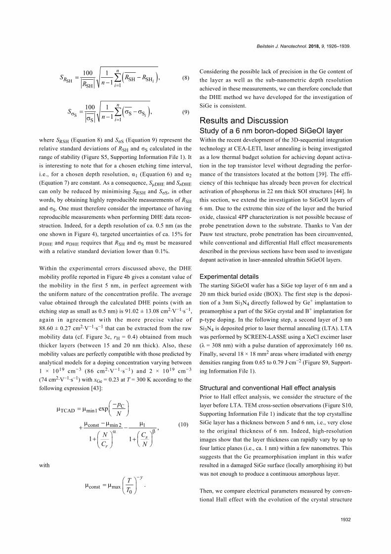
Figure 5: Sheet resistance as a function of the laser energy density for6 nm SiGeOI (xGe = 0.25) layer implanted with boron.
imaged by TEM as functions of the laser energy densities. The
TEM analysis (Figure S11, Supporting Information File 1)
shows that for energies of 0.74 and 0.76 J/cm2, the observed
structure is identical to that found in the as-implanted sample
with the SiGe layer being almost fully crystalline (and having a
surface roughness of about 1 nm). This suggests that the laser
energy density used in these cases is always lower than the
threshold value necessary to melt the surface. In contrast,
following a LTA at 0.79 J·cm−2 the SiGe top layer is complete-
ly amorphous, clearly indicating that in this case the whole
SiGe layer was molten, leaving no seed for a perfect recrystal-
lization. The threshold energy for surface melt is therefore lo-
cated between 0.76 and 0.79 J·cm−2 and a rapid transition be-
tween a “no melt” and a “full melt” configuration occurs in this
small energy interval.
Figure 5 reports the corresponding sheet-resistance measure-
ments as a function of the energy densities, which illustrates
two different behaviours. Below 0.74 J·cm−2, the sheet resis-
tance remains below 10 kΩ·sq−1, with a slight improvement
occurring when the energy density is increased (ca. 6000 Ω·sq−1
after LTA at 0.74 J·cm−2). This indicates that, although the laser
annealing did not melt the sample surface, a non-negligible
dopant activation occurs at these energies, as it will be dis-
cussed below. In contrast, a much higher sheet resistance value
(ca. 55 kΩ·sq−1) is measured in the sample annealed at
0.77 J·cm−2. Considering that the transition between “no melt”
and “full melt” of the 6 nm thick SiGe layer occurs between
0.76 and 0.79 J·cm−2, the high sheet resistance value measured
at 0.77 J·cm−2 suggests that a “full melt” of the SiGe layer has
already occurred at this energy and that most of the dopant acti-
vation is therefore lost. This behaviour is similar to that ob-
served by Acosta Alba et al. [44] in 22 nm thick phosphorus-
doped SOI, where the sudden increase in the sheet resistance
values observed for high laser energies was due to the forma-
tion of a poly-Si layer as a consequence of the full melt of the
entire top-Si layer during LTA.
For LTA energies below the melting threshold of 0.74 J·cm−2,
some dopant activation occurs. However, the Hall effect mea-
surements indicate that only a small fraction of the implanted
boron dose is electrically active (between 6 and 12%). Two
mechanisms contribute to this result: (i) the weak dopant pene-
tration through the Si3N4 capping layer during the implantation,
and (ii) the low activation rate due to the “non-melt” nature of
the LTA in this energy range.
In order to investigate the first point, we calculated by using
SRIM the depth distribution of the implanted boron ions ac-
cording to the process conditions used in this experiment. The
simulation results indicate that only about 45% of the implanted
boron dose is available for electrical activation during LTA, the
rest being lost in the Si3N4 capping layer or in the underlying
BOX. Still, the boron dose contained in the SiGe layer after the
implantation (ca. 1.8 × 1014 cm−2) is much higher than the
electrically active dose actually measured by Hall effect
(2.3 × 1013 cm−2 after LTA at 0.68 or 0.71 J·cm−2). In addition
to this “dose loss” mechanism during implantation, low dopant
activation must also occur during LTA.
Indeed, previous investigations [16,45] of dopant activation in-
dicated that under similar conditions, i.e., non-amorphising
implants and low thermal budget annealing (either conven-
tional RTA or non-melt LTA), the total active dose (measured
from SRP profiles) is much lower than the total implanted dose
(as measured by SIMS profiles). However, the few electrically
active dopant atoms present after annealing were not found to
be uniformly distributed in depth but rather mostly located close
to the surface, where the damage recovery, i.e., interstitial
recombination is favoured (Figure S12, Supporting Information
File 1). Moreover, even for the smallest thermal budgets (short
RTA time or minimum number of laser shots), dopant activa-
tion at the surface was maximum or close to the solubility limit
at the annealing temperature. Finally, it was found that dopant
activation increases with annealing time although no dopant
diffusion is detected by SIMS.
It is therefore important to verify if this behaviour also occurs in
the case of ultrathin laser-annealed SiGeOI samples. Indeed,
within the application of laser annealing in strategies to reduce
contact resistance, such a result may constitute a big step
forward. One of the LTA samples investigated in this work has
therefore been analysed by the differential Hall effect technique,
and results are presented in the next section.
Beilstein J. Nanotechnol. 2018, 9, 1926–1939.
1934
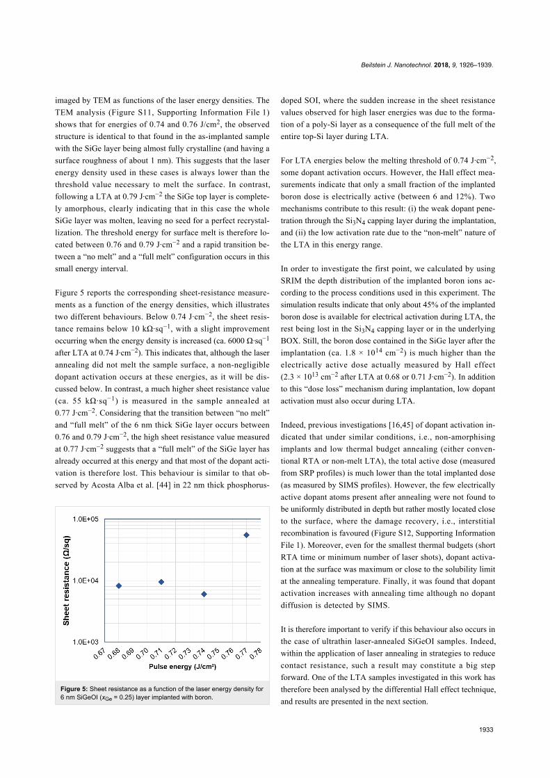
Figure 6: Hall effect measurements (raw data: (a) RS, (b) NH and (c) µH) of the SiGeOI sample (xGe = 0.25) implanted with boron and annealed at anenergy of 0.68 J·cm−2 as a function of the etched thickness (as measured by ellipsometry).
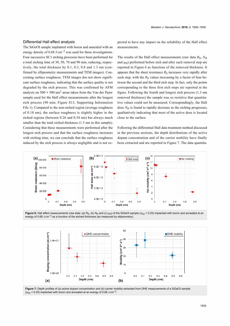
Figure 7: Depth profiles of (a) active dopant concentration and (b) carrier mobility extracted from DHE measurements of a SiGeOI sample(xGe = 0.25) implanted with boron and annealed at an energy of 0.68 J·cm−2.
Differential Hall effect analysisThe SiGeOI sample implanted with boron and annealed with an
energy density of 0.68 J·cm−2 was used for these investigations.
Four successive SC1 etching processes have been performed for
a total etching time of 30, 50, 70 and 90 min, reducing, respec-
tively, the total thickness by 0.1, 0.3, 0.8 and 1.3 nm (con-
firmed by ellipsometry measurements and TEM images). Con-
cerning surface roughness, TEM images dos not show signifi-
cant surface roughness, indicating that the surface quality is not
degraded by the etch process. This was confirmed by AFM
analysis on 500 × 500 nm2 areas taken from the Van der Pauw
sample used for the Hall effect measurements after the longest
etch process (90 min; Figure S13, Supporting Information
File 1). Compared to the non-etched region (average roughness
of 0.18 nm), the surface roughness is slightly higher in the
etched regions (between 0.26 and 0.34 nm) but always much
smaller than the total etched thickness (1.3 nm in this sample).
Considering that these measurements were performed after the
longest etch process and that the surface roughness increases
with etching time, we can conclude that the surface roughness
induced by the etch process is always negligible and is not ex-
pected to have any impact on the reliability of the Hall effect
measurements.
The results of the Hall effect measurements (raw data RS, NH
and µH) performed before etch and after each removal step are
reported in Figure 6 as functions of the removed thickness. It
appears that the sheet resistance RS increases very rapidly after
each step, with the RS values increasing by a factor of four be-
tween the second and the third etch step. In fact, only the points
corresponding to the three first etch steps are reported in the
figure. Following the fourth and longest etch process (1.3 nm
removed thickness) the sample was so resistive that quantita-
tive values could not be measured. Correspondingly, the Hall
dose NH is found to rapidly decrease as the etching progresses,
qualitatively indicating that most of the active dose is located
close to the surface.
Following the differential Hall data treatment method discussed
in the previous sections, the depth distributions of the active
dopant concentration and of the carrier mobility have finally
been extracted and are reported in Figure 7. The data quantita-

Beilstein J. Nanotechnol. 2018, 9, 1926–1939.
1935
Figure 8: Concentration depth profiles of (a) arsenic and (b) oxygen measured by SIMS in 11 nm thick SOI wafers implanted with arsenic andannealed by RTA (red curves) or DSA (blue curves).
tively confirm the results suggested by the Hall effect raw data:
The active dopant concentration is highest at the surface with a
value as high as ca. 6 × 1020 cm−3 and it rapidly decreases
within the first nanometres below the surface (2 × 1020 cm−3 at
0.8 nm). Corrections of the depth scale related due to the sur-
face-depletion effect have been neglected due to high doping
level measured in this sample (cf. previous section) unless we
give a numerical value.
This result is in agreement with the scenario discussed in the
previous section. Indeed, due to the “non-melt” nature of the
annealing, and considering that no amorphisation of the surface
was achieved during the implantation, the extremely low ther-
mal budget provided by the LTA process is not efficient in
removing the implant damage in the material, except in the sur-
face region where interstitial recombination (and hence damage
recovery) occurs. As a consequence, below the surface, not only
the active dopant concentration is much lower than at
the surface, but also the residual damage is extremely high,
which is expected to have an impact on the carrier mobility.
This is clearly confirmed by the Hall mobility (Figure 7b) the
value of which at a depth of 0.8 nm below the surface
(ca. 20 cm2·V−1·s−1) is much lower than the carrier mobility at
the surface (ca. 35 cm2·V−1·s−1), in spite of a much lower
carrier concentration. Alternative mechanisms as the reasons for
this mobility reduction below the surface can be excluded, in-
cluding surface roughness (Figure S13, Supporting Information
File 1), and surface depletion due to interface states (cf.
previous sections).
In any case, although the investigated doping process is at a pre-
liminary stage, the detailed investigation carried out in this
work allows us to conclude that a doping process based on
nanosecond-laser annealing can be successfully applied to
ultrathin SiGeOI layers of about 6 nm thickness, while obtain-
ing active dopant concentrations at the surface well above
1 × 1020 cm−3. This is a promising result in view of improving
contact resistivity in source/drain regions of advanced devices.
Study of 11 nm arsenic-doped SOI layerIn the perspective of improving the contact resistance within
FDSOI technology [6], different annealing methods are investi-
gated for the increase of dopant activation close to the surface.
In this section we will focus on the comparison between
conventional spike-RTA and millisecond-laser dynamic surface
annealing (DSA), both applied to 11 nm thick n-type doped SOI
layers. In addition to SIMS, TEM and conventional Hall effect
measurements, differential Hall profiling will be shown to allow
a reliable estimation of the dopant activation level within the
first nanometres below the silicon surface.
Experimental detailsTwo 11 nm thick SOI wafers were used for this experiment
(BOX thickness: 25 nm, as confirmed by ellipsometry). The
wafers were implanted with 3 keV As+ ions to a dose of
1 × 1014 cm−2. The implantations were performed through a
thin thermal oxide layer (ca. 1 nm thick) grown on the
as-received wafers. Following the implantations, each wafer
underwent a different annealing process: 1050 °C spike-RTA in
O2/N2 atmosphere in one case, 0.3 ms laser-DSA in N2 atmo-
sphere in the other case.
Chemical profiles and conventional Hall effectmeasurementsSIMS characterisations were carried out after annealing in both
samples without stripping the thermal oxide. The results are
shown in Figure 8 for both arsenic (Figure 8a) and oxygen
(Figure 8b). The As concentration profile of the RTA-annealed
wafer exhibits a peak value of ca. 3 × 1020 cm−3 just below the
surface, followed by a quasi-plateau (6–7 × 1019 cm−3) in the
Beilstein J. Nanotechnol. 2018, 9, 1926–1939.
1936
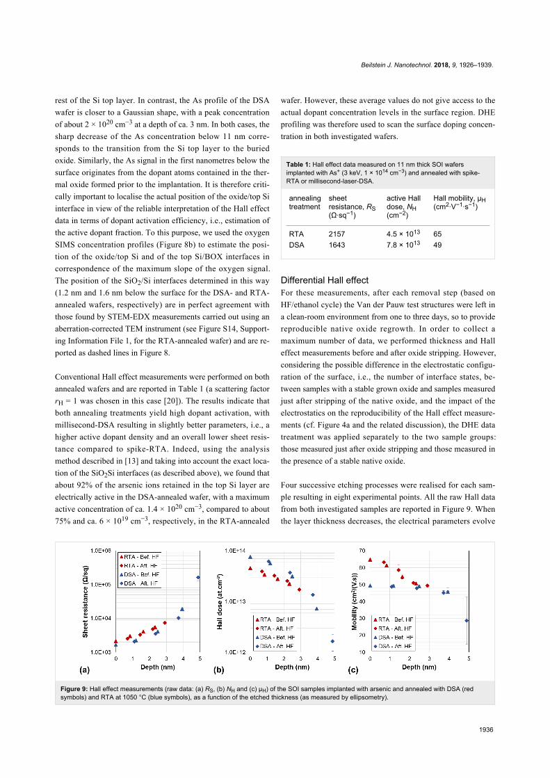
Figure 9: Hall effect measurements (raw data: (a) RS, (b) NH and (c) µH) of the SOI samples implanted with arsenic and annealed with DSA (redsymbols) and RTA at 1050 °C (blue symbols), as a function of the etched thickness (as measured by ellipsometry).
rest of the Si top layer. In contrast, the As profile of the DSA
wafer is closer to a Gaussian shape, with a peak concentration
of about 2 × 1020 cm−3 at a depth of ca. 3 nm. In both cases, the
sharp decrease of the As concentration below 11 nm corre-
sponds to the transition from the Si top layer to the buried
oxide. Similarly, the As signal in the first nanometres below the
surface originates from the dopant atoms contained in the ther-
mal oxide formed prior to the implantation. It is therefore criti-
cally important to localise the actual position of the oxide/top Si
interface in view of the reliable interpretation of the Hall effect
data in terms of dopant activation efficiency, i.e., estimation of
the active dopant fraction. To this purpose, we used the oxygen
SIMS concentration profiles (Figure 8b) to estimate the posi-
tion of the oxide/top Si and of the top Si/BOX interfaces in
correspondence of the maximum slope of the oxygen signal.
The position of the SiO2/Si interfaces determined in this way
(1.2 nm and 1.6 nm below the surface for the DSA- and RTA-
annealed wafers, respectively) are in perfect agreement with
those found by STEM-EDX measurements carried out using an
aberration-corrected TEM instrument (see Figure S14, Support-
ing Information File 1, for the RTA-annealed wafer) and are re-
ported as dashed lines in Figure 8.
Conventional Hall effect measurements were performed on both
annealed wafers and are reported in Table 1 (a scattering factor
rH = 1 was chosen in this case [20]). The results indicate that
both annealing treatments yield high dopant activation, with
millisecond-DSA resulting in slightly better parameters, i.e., a
higher active dopant density and an overall lower sheet resis-
tance compared to spike-RTA. Indeed, using the analysis
method described in [13] and taking into account the exact loca-
tion of the SiO2Si interfaces (as described above), we found that
about 92% of the arsenic ions retained in the top Si layer are
electrically active in the DSA-annealed wafer, with a maximum
active concentration of ca. 1.4 × 1020 cm−3, compared to about
75% and ca. 6 × 1019 cm−3, respectively, in the RTA-annealed
wafer. However, these average values do not give access to the
actual dopant concentration levels in the surface region. DHE
profiling was therefore used to scan the surface doping concen-
tration in both investigated wafers.
Table 1: Hall effect data measured on 11 nm thick SOI wafersimplanted with As+ (3 keV, 1 × 1014 cm−3) and annealed with spike-RTA or millisecond-laser-DSA.
annealingtreatment
sheetresistance, RS(Ω·sq−1)
active Halldose, NH(cm−2)
Hall mobility, µH(cm2·V−1·s−1)
RTA 2157 4.5 × 10¹³ 65DSA 1643 7.8 × 10¹³ 49
Differential Hall effectFor these measurements, after each removal step (based on
HF/ethanol cycle) the Van der Pauw test structures were left in
a clean-room environment from one to three days, so to provide
reproducible native oxide regrowth. In order to collect a
maximum number of data, we performed thickness and Hall
effect measurements before and after oxide stripping. However,
considering the possible difference in the electrostatic configu-
ration of the surface, i.e., the number of interface states, be-
tween samples with a stable grown oxide and samples measured
just after stripping of the native oxide, and the impact of the
electrostatics on the reproducibility of the Hall effect measure-
ments (cf. Figure 4a and the related discussion), the DHE data
treatment was applied separately to the two sample groups:
those measured just after oxide stripping and those measured in
the presence of a stable native oxide.
Four successive etching processes were realised for each sam-
ple resulting in eight experimental points. All the raw Hall data
from both investigated samples are reported in Figure 9. When
the layer thickness decreases, the electrical parameters evolve
Beilstein J. Nanotechnol. 2018, 9, 1926–1939.
1937
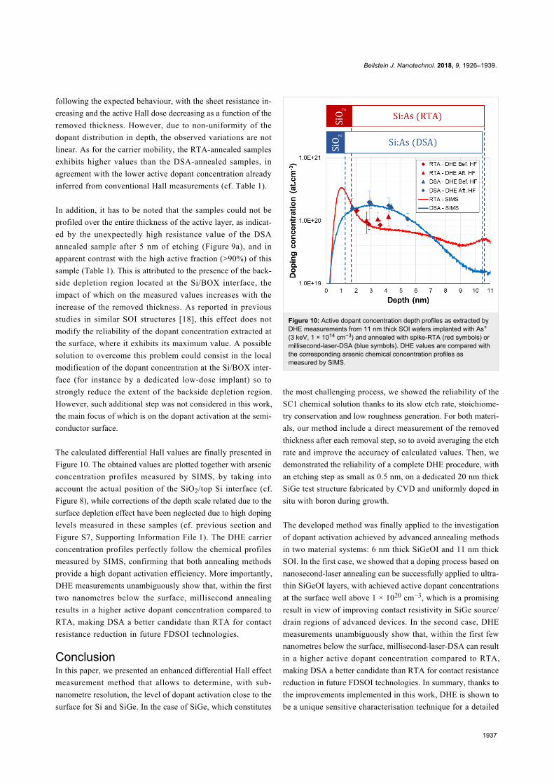
following the expected behaviour, with the sheet resistance in-
creasing and the active Hall dose decreasing as a function of the
removed thickness. However, due to non-uniformity of the
dopant distribution in depth, the observed variations are not
linear. As for the carrier mobility, the RTA-annealed samples
exhibits higher values than the DSA-annealed samples, in
agreement with the lower active dopant concentration already
inferred from conventional Hall measurements (cf. Table 1).
In addition, it has to be noted that the samples could not be
profiled over the entire thickness of the active layer, as indicat-
ed by the unexpectedly high resistance value of the DSA
annealed sample after 5 nm of etching (Figure 9a), and in
apparent contrast with the high active fraction (>90%) of this
sample (Table 1). This is attributed to the presence of the back-
side depletion region located at the Si/BOX interface, the
impact of which on the measured values increases with the
increase of the removed thickness. As reported in previous
studies in similar SOI structures [18], this effect does not
modify the reliability of the dopant concentration extracted at
the surface, where it exhibits its maximum value. A possible
solution to overcome this problem could consist in the local
modification of the dopant concentration at the Si/BOX inter-
face (for instance by a dedicated low-dose implant) so to
strongly reduce the extent of the backside depletion region.
However, such additional step was not considered in this work,
the main focus of which is on the dopant activation at the semi-
conductor surface.
The calculated differential Hall values are finally presented in
Figure 10. The obtained values are plotted together with arsenic
concentration profiles measured by SIMS, by taking into
account the actual position of the SiO2/top Si interface (cf.
Figure 8), while corrections of the depth scale related due to the
surface depletion effect have been neglected due to high doping
levels measured in these samples (cf. previous section and
Figure S7, Supporting Information File 1). The DHE carrier
concentration profiles perfectly follow the chemical profiles
measured by SIMS, confirming that both annealing methods
provide a high dopant activation efficiency. More importantly,
DHE measurements unambiguously show that, within the first
two nanometres below the surface, millisecond annealing
results in a higher active dopant concentration compared to
RTA, making DSA a better candidate than RTA for contact
resistance reduction in future FDSOI technologies.
ConclusionIn this paper, we presented an enhanced differential Hall effect
measurement method that allows to determine, with sub-
nanometre resolution, the level of dopant activation close to the
surface for Si and SiGe. In the case of SiGe, which constitutes
Figure 10: Active dopant concentration depth profiles as extracted byDHE measurements from 11 nm thick SOI wafers implanted with As+
(3 keV, 1 × 1014 cm−3) and annealed with spike-RTA (red symbols) ormillisecond-laser-DSA (blue symbols). DHE values are compared withthe corresponding arsenic chemical concentration profiles asmeasured by SIMS.
the most challenging process, we showed the reliability of the
SC1 chemical solution thanks to its slow etch rate, stoichiome-
try conservation and low roughness generation. For both materi-
als, our method include a direct measurement of the removed
thickness after each removal step, so to avoid averaging the etch
rate and improve the accuracy of calculated values. Then, we
demonstrated the reliability of a complete DHE procedure, with
an etching step as small as 0.5 nm, on a dedicated 20 nm thick
SiGe test structure fabricated by CVD and uniformly doped in
situ with boron during growth.
The developed method was finally applied to the investigation
of dopant activation achieved by advanced annealing methods
in two material systems: 6 nm thick SiGeOI and 11 nm thick
SOI. In the first case, we showed that a doping process based on
nanosecond-laser annealing can be successfully applied to ultra-
thin SiGeOI layers, with achieved active dopant concentrations
at the surface well above 1 × 1020 cm−3, which is a promising
result in view of improving contact resistivity in SiGe source/
drain regions of advanced devices. In the second case, DHE
measurements unambiguously show that, within the first few
nanometres below the surface, millisecond-laser-DSA can result
in a higher active dopant concentration compared to RTA,
making DSA a better candidate than RTA for contact resistance
reduction in future FDSOI technologies. In summary, thanks to
the improvements implemented in this work, DHE is shown to
be a unique sensitive characterisation technique for a detailed

Beilstein J. Nanotechnol. 2018, 9, 1926–1939.
1938
investigation of dopant activation in ultrashallow layers, provid-
ing sub-nanometre resolution for depth profiles of both dopant
concentration and carrier mobility.
Supporting InformationSupporting Information File 1Additional experimental data.
[https://www.beilstein-journals.org/bjnano/content/
supplementary/2190-4286-9-184-S1.pdf]
AcknowledgementsThis work is partly funded by the French public authorities
through the NANO 2017 program. This work has been carried
out thanks to French RENATECH network and to the micro and
nanotechnologies platform of LAAS-CNRS.
References1. Doris, B.; DeSalvo, B.; Cheng, K.; Morin, P.; Vinet, M.
Solid-State Electron. 2016, 117, 37–59. doi:10.1016/j.sse.2015.11.0062. James, D. Moore's Law Continues into the 1x-nm Era. In 2016 21st
International Conference on Ion Implantation Technology (IIT), Tainan,Taiwan, Sept 26–30, 2016; . doi:10.1109/IIT.2016.7882895
3. Larrieu, G.; Han, X.-L. Nanoscale 2013, 5, 2437–2441.doi:10.1039/c3nr33738c
4. Batude, P.; Vinet, M.; Xu, C.; Previtali, B.; Tabone, C.; Le Royer, C.;Sanchez, L.; Baud, L.; Brunet, L.; Toffoli, A.; Alain, F.; Lafond, D.;Aussenac, F.; Thomas, O.; Poiroux, T.; Faynot, O. Demonstration oflow temperature 3D sequential FDSOI integration down to 50 nm gatelength. In 2011 Symposium on VLSI Technology (VLSIT) – Digest ofTechnical Papers, Honolulu, HI, U.S.A., June 14–16, 2011; IEEEPublishing: Piscataway, NJ, U.S.A., 2011; pp 158–159.
5. Hutin, L.; Rozeau, O.; Carron, V.; Hartmann, J.-M.; Grenouillet, L.;Borrel, J.; Nemouchi, F.; Barraud, S.; Le Royer, C.; Morand, Y.;Plantier, C.; Batude, P.; Fenouillet-Béranger, C.; Boutry, H.; Ernst, T.;Vinet, M. Junction technology outlook for sub-28nm FDSOI CMOS. In2014 International Workshop on Junction Technology (IWJT),Shanghai, China, May 18–20, 2014; . doi:10.1109/IWJT.2014.6842050
6. Saraswat, K. C.; Shine, G. ECS Trans. 2016, 75, 513–523.doi:10.1149/07508.0513ecst
7. Colombeau, B.; Guo, B.; Gossman, H.-J.; Khaja, F.; Pradhan, N.;Waite, A.; Rao, K. V.; Thomidis, C.; Shim, K.-H.; Henry, T.; Variam, N.Phys. Status Solidi A 2014, 211, 101–108.doi:10.1002/pssa.201300169
8. Schroder, D. K. Resistivity. Semiconductor Material and DeviceCharacterization; Wiley-Interscience: Hoboken, NJ, U.S.A., 2006;pp 29–34.
9. Giannazzo, F.; Raineri, V.; La Magna, A.; Mirabella, S.; Impellizzeri, G.;Piro, A. M.; Priolo, F.; Napolitani, E.; Liotta, S. F. J. Appl. Phys. 2005,97, 014302. doi:10.1063/1.1827342
10. Giannazzo, F.; Raineri, V.; Mirabella, S.; Bruno, E.; Impellizzeri, G.;Priolo, F. Mater. Sci. Eng., B 2005, 124–125, 54–61.doi:10.1016/j.mseb.2005.08.076
11. Eyben, P.; Janssens, T.; Vandervorst, W. Mater. Sci. Eng., B 2005,124–125, 45–53. doi:10.1016/j.mseb.2005.08.049
12. Vandervorst, W.; Fleischmann, C.; Bogdanowicz, J.; Franquet, A.;Celano, U.; Paredis, K.; Budrevich, A. Mater. Sci. Semicond. Process.2017, 62, 31–48. doi:10.1016/j.mssp.2016.10.029
13. Severac, F.; Cristiano, F.; Bedel-Pereira, E.; Fazzini, P.-F.; Boucher, J.;Lerch, W.; Hamm, S. J. Appl. Phys. 2010, 107, 123711.doi:10.1063/1.3446844
14. Giannazzo, F.; Raineri, V.; Mirabella, S.; Impellizzeri, G.; Priolo, F.Appl. Phys. Lett. 2006, 88, 043117. doi:10.1063/1.2168502
15. Sermage, B.; Essa, Z.; Taleb, N.; Quillec, M.; Aubin, J.;Hartmann, J. M.; Veillerot, M. J. Appl. Phys. 2016, 119, 155703.doi:10.1063/1.4946890
16. Fisicaro, G.; Pelaz, L.; Aboy, M.; Lopez, P.; Italia, M.; Huet, K.;Cristiano, F.; Essa, Z.; Yang, Q.; Bedel-Pereira, E.; Quillec, M.;La Magna, A. Appl. Phys. Express 2014, 7, 021301.doi:10.7567/APEX.7.021301
17. Blight, S. R.; Nicholls, R. E.; Sangha, S. P. S.; Kirby, P. B.; Teale, L.;Hiscock, S. P.; Stewart, C. P. J. Phys. E: Sci. Instrum. 1988, 21,470–479. doi:10.1088/0022-3735/21/5/011
18. Bennett, N. S.; Smith, A. J.; Colombeau, B.; Gwilliam, R.;Cowern, N. E. B.; Sealy, B. J. Mater. Sci. Eng., B 2005, 124–125,305–309. doi:10.1016/j.mseb.2005.08.020
19. Qin, S.; Prussin, S. A.; Reyes, J.; Hu, Y. J.; McTeer, A.IEEE Trans. Plasma Sci. 2011, 39, 587–592.doi:10.1109/TPS.2010.2089702
20. Alzanki, T.; Gwilliam, R.; Emerson, N.; Sealy, B. J. Appl. Phys. Lett.2004, 85, 1979–1980. doi:10.1063/1.1792378
21. Bennett, N. S.; Cowern, N. E. B.; Smith, A. J.; Kah, M.; Gwilliam, R. M.;Sealy, B. J.; Noakes, T. C. Q.; Bailey, P.; Giubertoni, D.; Bersani, M.Mater. Sci. Eng., B 2008, 154–155, 229–233.doi:10.1016/j.mseb.2008.10.003
22. Ling, Y.-T.; Su, W.-T.; Pi, T.-W.; Chang, R.-D. AIP Conf. Proc. 2012,1496, 152. doi:10.1063/1.4766512
23. Bennett, N. S.; Cowern, N. E. B. Appl. Phys. Lett. 2012, 100, 172106.doi:10.1063/1.4705293
24. LeGoues, F. K.; Rosenberg, R.; Nguyen, T.; Himpsel, F.;Meyerson, B. S. J. Appl. Phys. 1989, 65, 1724–1728.doi:10.1063/1.342945
25. Johnson, F. S.; Miles, D. S.; Grider, D. T.; Wortman, J. J.J. Electron. Mater. 1992, 21, 805–810. doi:10.1007/BF02665519
26. Stoffel, M.; Malachias, A.; Merdzhanova, T.; Cavallo, F.; Isella, G.;Chrastina, D.; Von Känel, H.; Rastelli, A.; Schmidt, O. G.Semicond. Sci. Technol. 2008, 23, 1–6.doi:10.1088/0268-1242/23/8/085021
27. Gavelle, M. Etude expérimentale de l’interdiffusion Ge-Si à partir desources solides Germanium sur Silicium - Application à la formation decouches graduelles Si1-xGex pour les transistors pMOSFETs. Ph.D.Thesis, University of Toulouse, Toulouse, France, 2008; pp 168–183.
28. Garrido, B.; Gessinn, F.; Prom, J. L.; Morante, J. R.; Samitier, J.;Sarrabayrousse, G. Silicon Surface Analysis and Very Thin SiliconOxide Characterization after HF/Ethanol Preoxidation Silicon Cleaning.In The Physics and Chemistry of SiO2 and the Si-SiO2 Interface 2;Deal, B. E.; Helms, C. R., Eds.; Springer: Boston, MA, U.S.A., 1993;pp 215–222. doi:10.1007/978-1-4899-1588-7_23
29. Van der Pauw, L. J. Philips Tech. Rev. 1958, 20, 220–224.30. Haeusler, J.; Lippman, H. J. Solid-State Electron. 1968, 11, 173–182.
doi:10.1016/0038-1101(68)90149-431. De Mey, G. Arch. Elektron. Übertragungstechnik 1973, 27, 309–313.32. David, J. M.; Buehler, M. G. Solid-State Electron. 1977, 20, 539–543.
doi:10.1016/S0038-1101(77)81011-3

Beilstein J. Nanotechnol. 2018, 9, 1926–1939.
1939
33. McGregor, J. M.; Manku, T.; Noël, J.-P.; Roulston, D. J.; Nathan, A.;Houghton, D. C. J. Electron. Mater. 1993, 22, 319–321.doi:10.1007/BF02661384
34. Carns, T. K.; Tanner, M. O.; Wang, K. L. J. Electrochem. Soc. 1995,142, 1260–1266. doi:10.1149/1.2044161
35. Joelsson, K. B.; Fu, Y.; Ni, W.-X.; Hansson, G. V. J. Appl. Phys. 1997,81, 1264–1269. doi:10.1063/1.363906
36. Tabe, M.; Kumezawa, M.; Ishikawa, Y. Jpn. J. Appl. Phys. 2001, 40,L131–L133. doi:10.1143/JJAP.40.L131
37. Diarra, M.; Niquet, Y.-M.; Delerue, C.; Allan, G. Phys. Rev. B 2007, 75,1–4. doi:10.1103/PhysRevB.75.045301
38. Björk, M. T.; Schmid, H.; Knoch, J.; Riel, H.; Riess, W.Nat. Nanotechnol. 2009, 4, 103–107. doi:10.1038/nnano.2008.400
39. Pasini, L.; Batude, P.; Lacord, J.; Casse, M.; Mathieu, B.; Sklenard, B.;Piegas Luce, F.; Micout, J.; Payet, A.; Mazen, F.; Besson, P.;Ghegin, E.; Borrel, J.; Daubriac, R.; Hutin, L.; Blachier, D.; Barge, D.;Chhun, S.; Mazzocchi, V.; Cros, A.; Barnes, J.-P.; Saghi, Z.;Delaye, V.; Rambal, N.; Lapras, V.; Mazurier, J.; Weber, O.;Andrieu, F.; Brunet, L.; Fenouillet-Beranger, C.; Rafhay, Q.;Ghibaudo, G.; Cristiano, F.; Haond, M.; Boeuf, F.; Vinet, M. Highperformance CMOS FDSOI devices activated at low temperature. InIEEE Symposium on VLSI Technology, Honolulu, HI, U.S.A., June14–16, 2016; IEEE Publishing: Piscataway, NJ, U.S.A., 2016.doi:10.1109/VLSIT.2016.7573407
40. Pasini, L. Optimisation des jonctions de dispositifs (FDSOI, TriGate)fabriqués à faible température pour l’intégration 3D séquentielle. Ph.D.Thesis, University Grenoble Alpes, Grenoble, France, 2016; pp 88–96.
41. Kooi, E. The surface properties of oxidized silicon. Ph.D. Thesis,Technische Hogeschool Eindhoven, Eindhoven, Netherlands, 1967;pp 5–9. doi:10.1007/978-3-662-40210-8
42. Yeo, Y. K.; Hengehold, R. L.; Elsaesser, D. W. J. Appl. Phys. 1987, 61,5070–5075. doi:10.1063/1.338331
43. TCAD Sentaurus Process User Guide, I-2013.12 version; Synopsis,Inc.: Mountain View, CA, U.S.A., 2013.
44. Acosta Alba, P.; Kerdilès, S.; Mathieu, B.; Kachtouli, R.;Mazzamuto, F.; Toque-Tresonne, I.; Huet, K.; Besson, P.; Veillerot, M.;Aussenac, F.; Fenouillet-Béranger, C. Nanosecond Laser Annealing forPhosphorous Activation in Ultra-Thin Implanted Silicon-On-InsulatorSubstrates. In 2016 21st International Conference on Ion ImplantationTechnology (IIT), Tainan, Taiwan, Sept 26–30, 2016; IEEE Publishing:Piscataway, NJ, U.S.A., 2016. doi:10.1109/IIT.2016.7882896
45. Hebras, X. Contributions à l’étude de la diffusion, de l’agglomération etde l’activation du Bore dans le Silicium: Application à la réalisation dejonctions ultraminces P+/N. Ph.D. Thesis, University of Toulouse,France, Toulouse, France, 2003; pp 127–138.
License and TermsThis is an Open Access article under the terms of the
Creative Commons Attribution License
(http://creativecommons.org/licenses/by/4.0), which
permits unrestricted use, distribution, and reproduction in
any medium, provided the original work is properly cited.
The license is subject to the Beilstein Journal of
Nanotechnology terms and conditions:
(https://www.beilstein-journals.org/bjnano)
The definitive version of this article is the electronic one
which can be found at:
doi:10.3762/bjnano.9.184