a developed structure of step-up dc/dc converter by using coupled inductor...
TRANSCRIPT

Journal of Operation and Automation in Power Engineering
Vol. 5, No. 1, June 2017, Pages: 31-42
http://joape.uma.ac.ir
A Developed Structure of Step-Up DC/DC Converter by Using Coupled
Inductor and Active-Clamped Circuit
E. Babaei*, Gh. Mostafai Baruji, H. Mashinchi Maheri, A. Abbasnezhad
Faculty of Electrical and Computer Engineering, University of Tabriz, Tabriz, Iran
Abstract- In this paper, a new structure of step-up dc-dc converter by using coupled inductor and active-
clamped circuit is proposed. The proposed converter generates high voltage gain in comparison with the
conventional dc-dc converters. Due to using active-clamped circuit in the proposed topology, the voltage stress
on main switch is reduced. In addition, the zero voltage switching (ZVS) in ON-state of main switch is obtained.
In this paper, the performance of the proposed structure is investigated in continuous current mode (CCM) and
discontinuous current mode (DCM). Moreover, the voltage gains in CCM and DCM operations are calculated.
To prove the correctness operation and also the given equations, the simulation results in PSCAD/EMTDC
software are used.
Keyword: Coupled-inductor, Step-up converter, Active-clamped circuit, Zero voltage switching
1. INTRODUCTION In recent years, due to quick increasing in energy
consumption, the distributed generation (DG)
systems such as fuel cell, photovoltaic and wind
energy have been noticed [1-2]. Produced voltage
through fuel cell and photovoltaic is DC and has a
low magnitude. So, a step-up DC-DC converter is
used as an interface device between source and
inverter to transform voltage from a low level to a
high level. This converter must include high voltage
gain, high efficiency and small volume [3]. The
conventional step-up converters produce a high
voltage gain with a very large duty cycle [4-7].
Operating with high duty cycle may cause reverse
recovery and electromagnetic interface problems [8].
Moreover, in practice, the voltage gain is restricted
due to existence of power switch, rectifier diode and
equivalent series resistor of inductors and capacitors.
The voltage gain can be improved by using the dc-dc
converters with capacitive or inductive switching
construction [9]. Additionally, a small resonant
inductor is added into the switched-capacitor circuit
to solve the diode reverse recovery problem and
reduced the large pulsed current across the switches
when being turned ON [10-11]. Also an inactive
chopper circuit with low losses which is a
combination of diode and capacitor is used to cut the
Received: 14 Mar. 2014
Revised: 9 Sep. 2015 and 28 Jan. 2016.
Accepted: 12 June 2016
*Corresponding author: [email protected] (E.
Babaei)
2017 University of Mohaghegh Ardabili. All rights reserved.
voltage spike in OFF-state of switch and then
recover energy of the leakage inductor [3].
Moreover, several step-up inductor-based converters
and converters with inactive low loss chopper circuit
can be used [12-15]. In these structures, the switches
operate in hard switching condition. In some of these
converters, the high voltage gain is produced by
regulating the conversion ratio Nevertheless, the
main switch may face with short-term transient
voltage (voltage spike) and the transformer leakage
inductance causes high power losses. To increase the
efficiency and to reach a high voltage gain, new
step-up converters have been introduced in [16-17].
In these converters the switch faces high charge
current and transmission losses. In DC-DC
converters coupling inductor is used to get high
voltage gain, but it must be noted that the leakage
inductance causes a short-term transient voltage
through main switch and impresses conversion ratio
[13, 18, 19]. Moreover, voltage multiplier cell could
be used to increase the voltage gain [15]. Also, the
voltage gain can be increased by utilizing several
coupling inductors [20-22]. In [23] a high step-up
dc-dc converter has been presented. In the proposed
structure in order to have a high voltage gain a diode
and a capacitor has been used in the input. In the
proposed structure a passive clamp circuit has been
used to provide zero voltage switching (ZVS)
condition.
In this paper, a new structure for active clamp
coupled-inductor-based converter is proposed. The
Proposed structure has a high voltage gain and low
ripple of input current. At the following, first the
operation of the proposed converter in different
operating modes in continuous current mode (CCM)
and discontinuous current mode (DCM) is given.
Then, the voltage gain of the converter is calculated.

E. Babaei et al.: A Developed Structure of Step-Up DC/DC Converter by Using Coupled … 32
Finally, the correctness operation of the proposed
converter is reconfirmed by the simulation results in
PSCAD/EMTDC software.
2. PROPOSED CONVERTER
Figure 1 shows the configuration of proposed
converter including input DC voltage source ( iV ),
main switch ( S ), clamp circuit which is consisted of
an auxiliary switch (Sc) and a capacitor (Cc),
coupling inductors NS and Np, capacitors C2 and C3 ,
diodes 2D and D3, output diode ( )oD and output
capacitor (Co). The coupling inductor is used as a
transformer in converter. Equivalent circuit of
coupling inductors contains magnetizing inductor
Lm, leakage inductor LK and an ideal transformer.
Parasitic capacitor is used to Zero Voltage Switching
(ZVS). The Energy of the leakage inductance of the
coupling inductor is returned to the capacitor oC
and then, the voltage stress decreases through the
switch ( )S , so, a switch with low ON-state resistor
(,DS onR ) could be used.
The converter operates in a way that when the
main switch is in ON-state the magnetizing
inductance Lm is charged by iV . So, the magnetizing
current increases linearly and at the same time the
energy is transferred to the switched-capacitors 2C
and 3C through the coupling inductors. When the
switch is off the stored energy in the magnetizing
inductor Lm is released through the secondary side of
coupling inductor to charge the capacitors 2C and
3C in parallel state. The current of secondary
winding is limited by leakage inductance.
The following assumptions are considered to
simplify the analysis of the proposed converter:
1) The capacitors 2C , 3C and oC have enough
large magnitude. As a result, the voltages
2cV , 3cV and oV is considered constant.
2) The switches are considered but the parasitic
capacitor of switch is considered.
3) The conversion ratio of the coupling inductor
is assumed as follows:
s
p
Nn
N (1)
At the following subsections, the operation of the
proposed converter is considered in CCM and DCM.
Fig. 1. Proposed dc/dc converter.
2.1. Operation in CCM
In CCM operation, there are eight operating modes
at every switching period. Fig. 2 shows the typical
waveforms of converter in CCM operation and
Fig. 3 shows the equivalent circuit of converter in
different operating modes in CCM operation.
A. Subinterval ( 0 1t t )
In this operating mode, the main switch S is in ON-
state and the clamp switch cS and output diode oD
are in OFF-state. The magnetizing inductor and
leakage inductors are going to be charged through
the input voltage source. So, the magnetic current
increases linearly. The voltage equation of leakage
and magnetizing inductors in the primary side is as
i Lk LmV V V . The Secondary side current ( )si
increases with respect to the leakage inductor and
energy is transferred to capacitors 2C and 3C
through the coupling inductor at the same time. The
output capacitor oC is discharged by the load R .
Therefore, the currents LmI and LKI are obtained as
follows:
10 0( ) ( ) ( )i L
Lm Lm
m
V Vi t i t t t
L
(2)
2
0 0( ) (( ) )
ci
Lk LK
LK
VV
ni t i t t tL
(3)
B. Subinterval ( 1 2t t )
The main switch ( )S turns OFF at moment 1t , then
the capacitor sC begins to resonant with leakage
inductance KL . Since sC is small and KL is
relatively large, the voltage dsV on main switch S
rises almost at a constant of zero. Turn-off losses of
main switch are reduced due to the existence of sC .
11
( )( )Lk
ds
s
i tV t t
C (4)
C. Subinterval ( 2 3t t )
According to Fig. 2 at 2t , the switching voltage of
main switch reaches the clamp capacitor voltage,
and the antiparallel of clamp switch cS is forced to
conduct. Then, dsV is clamped to CcV by the
antiparallel diode of clamp switch cS .
Since clamp capacitor cC is much large than sC ,
so sC can be neglected and almost all the current
flow through the cC . After 2t , the leakage
inductance kL is discharged by the voltage of
2[ ( / )]i c CcV V n V that is shown in Fig. 2. In
comparison with CcV , the voltage of 2( / )i cV V n
2D
3D
oD
2Cv 2Lv 3Cv
2C SN3C
CCCCv
CS
S
PN
mL
KL
1Lv oCov
R
Doi
Lki
Lkv
iV
3Di
2Di

Journal of Operation and Automation in Power Engineering, Vol. 5, No. 1, June 2017 33
is much smaller and it can be neglected to simplify
the expression. In this short subinterval, the current
through LkL decreases almost linearly, as well as the
current through secondary winding.
Considering the above-mentioned discussion, the
followed equations can be written:
2
2 2( )()
ci Cc
Lk
K
LK
VV V
ni t i t t tL
(5)
2 2( )) ( )( CcLk Lk
K
Vi t i t t t
L (6)
According to Fig. 2, in the third operating mode
(t2 < t < t3), the waveform of the current through the
leakage inductor has a steep slope which can cause a
voltage spike across the inductor in a short time
interval. However, in this operating mode, despite
the steep slope of the current waveform, the absolute
value of the current difference is low, which limits
the voltage across the inductor. In addition,
according to Eq. (6), the voltage across the leakage
inductor is limited to VCc, which is a constant value
and it can not be considered as a spike.
D. Subinterval (t3 – t4)
At moment t3 the voltage across the output diode
oD falls to zero, then the stored energy is
transferred to the load.
Lm is discharged and during this time interval the
leakage inductance LK is begins to resonate with
capacitor Cc and capacitors C2 and C3. In this time
interval, the resonance is relatively large and the
leakage inductance current decreases linearly. For
the operating mode, the following equations can be
written:
3
3 23
)
(
( ( )
)
Lm Lm
o Cc C C
m
i t i t
V V V Vt t
nL
(7)
3
3 2
3
)
(
( ( )
)
LK LK
o c ci C
K
c
i t i t
V V VV V
nt t
L
(8)
E. Subinterval (t4 – t5)
Turn-On signal is applied to clamp switch Sc at t4. Sc
is turned on when its body diode is conducting thus
the ZVS turn-on condition is achieved. The
Equivalent circuit in this subinterval is similar to
that of subinterval (t3 – t4).
Fig. 2. Typical waveforms of the proposed converter in CCM
operation.
(a)
(b)
2D
3D
oD
2Cv 2Lv 3Cv
2C SN3C
CCCCv
CS
PN
mL
KL
1Lv oCov
R
Doi
Lki
Lkv
iV
3Di
2DiS
SC
2D
3D
oD
2Cv 2Lv 3Cv
2C SN3C
CCCCv
CSS
PN
mL
KL
1Lv oCov
R
Doi
Lki
Lkv
iV
3Di
2Di
1t 2t 3t 4t 5t6t 7t 8t 9t
Lki
t
Cci
t2 3,C Ci i
t
2 3,D Di i
tDoi
tot
t
Si
dscV
t
t
SCi
Dov
t
t
ScS S cS
D1 Dgi
dsV
t
CcV
CcV
1( )Lki t
1( )Lmi tLmi
t
2( )Lki t
2 3,D Dv v
t
2o CV V
2o C CCV V V
2o CV V
2o C CcV V V
ZVS
ZVS
E. Babaei et al.: A Developed Structure of Step-Up DC/DC Converter by Using Coupled … 34
(c)
(d)
(e)
(f)
(g)
(h)
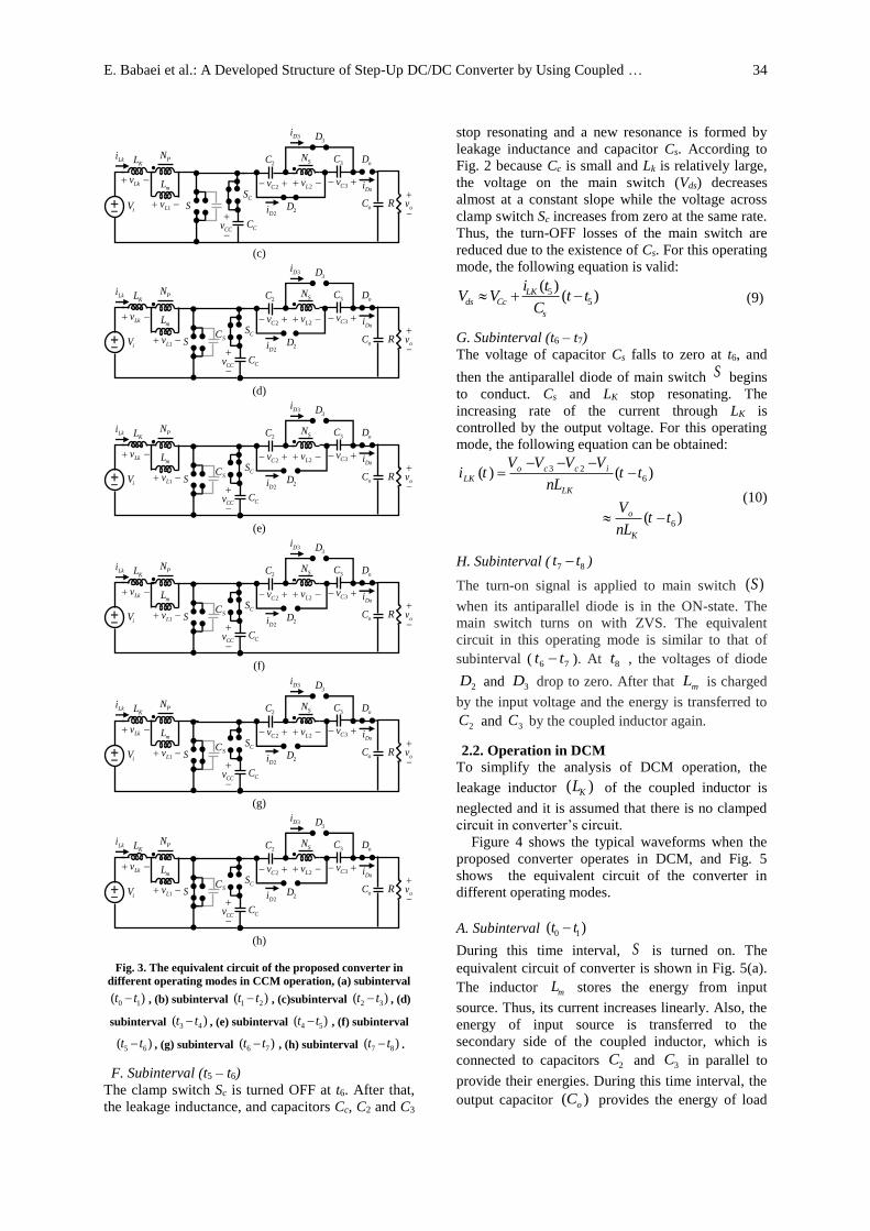
Fig. 3. The equivalent circuit of the proposed converter in
different operating modes in CCM operation, (a) subinterval
0 1( )t t , (b) subinterval 1 2( )t t , (c)subinterval 2 3( )t t , (d)
subinterval 3 4( )t t , (e) subinterval 4 5( )t t , (f) subinterval
5 6( )t t , (g) subinterval 6 7( )t t , (h) subinterval 7 8( )t t .
F. Subinterval (t5 – t6)
The clamp switch Sc is turned OFF at t6. After that,
the leakage inductance, and capacitors Cc, C2 and C3
stop resonating and a new resonance is formed by
leakage inductance and capacitor Cs. According to
Fig. 2 because Cc is small and Lk is relatively large,
the voltage on the main switch (Vds) decreases
almost at a constant slope while the voltage across
clamp switch Sc increases from zero at the same rate.
Thus, the turn-OFF losses of the main switch are
reduced due to the existence of Cs. For this operating
mode, the following equation is valid:
55
((
))LK
ds Cc
s
i tV V t t
C
(9)
G. Subinterval (t6 – t7)
The voltage of capacitor Cs falls to zero at t6, and
then the antiparallel diode of main switch S begins
to conduct. Cs and LK stop resonating. The
increasing rate of the current through LK is
controlled by the output voltage. For this operating
mode, the following equation can be obtained:
3 26
6
( ) ( )
( )
o c c iLK
LK
o
K
V V V Vi t t t
nL
Vt t
nL
(10)
H. Subinterval ( 7 8t t )
The turn-on signal is applied to main switch ( )S
when its antiparallel diode is in the ON-state. The
main switch turns on with ZVS. The equivalent
circuit in this operating mode is similar to that of
subinterval ( 6 7t t ). At 8t , the voltages of diode
2D and 3D drop to zero. After that mL is charged
by the input voltage and the energy is transferred to
2C and 3C by the coupled inductor again.
2.2. Operation in DCM
To simplify the analysis of DCM operation, the
leakage inductor ( )KL of the coupled inductor is
neglected and it is assumed that there is no clamped
circuit in converter’s circuit.
Figure 4 shows the typical waveforms when the
proposed converter operates in DCM, and Fig. 5
shows the equivalent circuit of the converter in
different operating modes.
A. Subinterval 0 1( )t t
During this time interval, S is turned on. The
equivalent circuit of converter is shown in Fig. 5(a).
The inductor mL stores the energy from input
source. Thus, its current increases linearly. Also, the
energy of input source is transferred to the
secondary side of the coupled inductor, which is
connected to capacitors 2C and 3C in parallel to
provide their energies. During this time interval, the
output capacitor ( )oC provides the energy of load
2D
3D
oD
2Cv 2Lv 3Cv
2C SN3C
CCCCv
CS
PN
mL
KL
1Lv oCov
R
Doi
Lki
Lkv
iV
3Di
2DiS
SC
2D
3D
oD
2Cv 2Lv 3Cv
2C SN3C
CCCCv
CS
PN
mL
KL
1Lv oCov
R
Doi
Lki
Lkv
iV
3Di
2DiS
SC
2D
3D
oD
2Cv 2Lv 3Cv
2C SN3C
CCCCv
CS
PN
mL
KL
1Lv oCov
R
Doi
Lki
Lkv
iV
3Di
2DiS
SC
2D
3D
oD
2Cv 2Lv 3Cv
2C SN3C
CCCCv
CS
PN
mL
KL
1Lv oCov
R
Doi
Lki
Lkv
iV
3Di
2DiS
SC
2D
3D
oD
2Cv 2Lv 3Cv
2C SN3C
CCCCv
CS
PN
mL
KL
1Lv oCov
R
Doi
Lki
Lkv
iV
3Di
2DiS
SC
2D
3D
oD
2Cv 2Lv 3Cv
2C SN3C
CCCCv
CSS
PN
mL
KL
1Lv oCov
R
Doi
Lki
Lkv
iV
3Di
2Di

Journal of Operation and Automation in Power Engineering, Vol. 5, No. 1, June 2017 35
lonely. This operating mode ends when switch ( )S
is turned off at 1t t .
B. Subinterval 1 2( )t t
During this time interval, S is turned off. The
equivalent is shown in Fig. 5(b). The secondary side
of the coupled inductor is connected to capacitors
2C and 3C in series. The energy of inductor mL is
transferred to load and output capacitor by the
secondary side of the coupled inductor. Also both
the capacitors 2C and 3C is connected in series
with the secondary side of the coupled inductor to
provide the energy of load and capacitor oC . This
operating mode ends when the energy stored in mL
is depleted at 2t t .
C. Subinterval 2 3( )t t
During this time interval, S remains turned off. The
equivalent circuit is shown in Fig. 5(c). Since the
energy stored in mL is depleted, the energy stored in
oC is discharged to load R . This mode ends when
S is turned on at 3t t .
Fig. 4. Typical waveforms of the proposed converter at DCM
operation.
(a)
(b)
(c)
Fig. 5. Equivalent circuit of proposed converter for different
types of operation mode, (a) subinterval1 0 1( )t t , (b)
subinterval2 1 2( )t t , (c) subinterval3 2 3( )t t .
3. VOLTAGE GAIN CALCULATION
3.1. CCM operation
In Figure 2 at subinterval ( 1 4t t ) and ( 5 8t t ), the
operation is very quick. So, these operating modes
can be neglected in voltage gain calculations. The
ideal current of leakage inductor is considered linear
and constant and the resonance is relatively large at
switching period. There are two kinds of separate
operation at total switching period. The main switch
is off at subinterval ( 1 5t t ) and clamp switch is on.
The current of oD , 2D and 3D diodes are equal to
output current ( )oI . The current peak of output
diode is:
2
1
oDo peak
II
D
(11)
For fifth operating mode the following equations
can be written:
1 5 1
Do peak
K K
s
L t
nI fV L
D
(12)
1 5 2
2
1
K o sLK t
nL I fV
D
(13)
1 5
2 3 2o Cc c c L
tV V V V V (14)
2
V
L Lm dischargeV nV (15)
1 5
1 51L discharge K
t
Cc i L tV V V V
(16)
By applying voltage balance law for inductor mL
we have:
0
0offon
on
TT
i i Cc
T
Vdt V V dt (17)
From above equation, the following equation is
obtained:
1 0s i i Cc SDTV D V V T (18)
Where D denotes duty cycle.
Simplifying Eq. (18):
1
1Cc iV V
D
(19)
The main switch is in ON-state at subinterval
( 5 9t t ) and clamp switch is in off-state. The current
peak of diodes 1D and 2D , The voltages of leakage
inductor and capacitors are achieved as below:
2D
3D
oD
2Cv 2Lv 3Cv
2C SN3C
S
PN
mL
1Lv oCov
R
Doi
iV
3Di
2Di
2D
3D
oD
2Cv 2Lv 3Cv
2C SN3C
S
PN
mL
1Lv oCov
R
Doi
iV
3Di
2Di
2D
3D
oD
2Cv 2Lv 3Cv
2C SN3C
S
PN
mL
1Lv oCov
R
Doi
iV
3Di
2Di
sDT
sT
gsv
0
0
01t
t
t
t
L sD T
1Li
1L PI
1
2L PI
n
0t 2t 3t
2Di

E. Babaei et al.: A Developed Structure of Step-Up DC/DC Converter by Using Coupled … 36
2
2 oD peak
II
D (20)
5 9
2D peak s
t KLK
nI fV L
D
(21)
5 9 2
2 o sLK t
KnL I fV
D (22)
5 9 5 93C t i LK tV n V V (23)
5 9 5 92C t i LK tV n V V (24)
By substituting Eqs. (17), (19), (23) and (24) into
Eq. (15), the voltage gain is obtained as below by
considering leakage inductor:
2
2
2
21
1
2
21
1 1
s oo i i
s oi
s oi
K
i
K
K
nL f IV V n V
D D
nL f In V
D
nL f In V V
D D
(25)
The output current is:
oo
VI
R (26)
The following equation is refined:
LK sm
L fk
R (27)
where sf is frequency.
By substituting Eq. (27) in Eq. (25) the voltage
gain is obtained as below:
2
2
2
2
)1(
241
1
1
)2(1
D
Kn
D
KnD
Dn
V
VM
mm
i
oCCM
(28)
Assuming 0mk the voltage gain will be:
1 2
1
oCCM
i
V n nDM
V D
(29)
Considering Eq. (29) the duty cycle is obtained as
follows:
1 2o i
o i
V n VD
V nV
(30)
Substituting Eq. (30) in Eq. (19) yields:
1
o iCc
V nVV
n
(31)
If conversion ratio of the coupling inductor is
considered zero, so the voltage gain will be same
with the conventional boost converter. The voltage
gain increases by increasing conversion ratio of
coupling inductor and decreases when coupling
inductance increases. Assuming 1mk , voltage
gain is:
2 2
2 2
1 (2 ) 1
1 4 21
(1 )
oCCM
i
V n DM
V D n n
D D
(32)
Fig. 6. Variations of voltage gain versus duty cycle under
CCM operation with 1n , 3n and 0mk .
The variations of voltage gain ( /o iV V ) versus
duty cycle ( D ) for different values of conversion
ratio is illustrated in Fig. 6. As shown in this figure
by increasing the conversion ratio, the voltage gain
increase.
3.2. DCM Operation
For DCM operation, the following equations are
valid for subinterval (t0-t1):
1L inv V (33)
2L inv nV (34)
2 3 2C C LV V v (35)
2 3C C inV V nV (36)
The peak value of the magnetizing-inductor
current is calculated as:
iLmP s
m
VI DT
L (37)
In interval 1 2[ ]t t , the following equation can be
expressed based on Fig. 5(b):
2 31
1
i o C CL
V V V Vv
n
(38)
Substituting (36) into (38):
1
(1 2 )
1
i oL
n V Vv
n
(39)
In time interval 2 3( )t t , the following equation
can be derived from Fig. 5(c):
1 2 0L Lv v (40)
By applying the voltage-second balance principle
to the coupled inductor, the following equation is
obtained:
0 0.2 0.4 0.6 0.8 10
10
20
30
40
1
3
n
n
o
i
V
V
D

Journal of Operation and Automation in Power Engineering, Vol. 5, No. 1, June 2017 37
01
0
)(
)(111
sDT sTLDD
sDT
sT
sTLDDLLL dtvdtvdtv
T (41)
Substituting Eqs. (33), (38), and (40) into Eq. (41),
the voltage gain is calculated as follows:
[1 (2 ) (1 2 )]
1
Lo i
L
D n D nV V
D D
(42)
According to Eq. (42), the duty cycle LD as
defined in Fig. 4 can be derived as below:
[1 (2 ) ] (1 )
(1 2 )
i oL
i o
V D n D VD
n V V
(43)
From Fig. 5, the energy stored on capacitor 2C is
fully released to capacitor oC . Also, the average
current DoI is equal to 2DI . Thus, the average
current of CoI is computed as:
2
1
2 2
LmPCo Do o D o s
II I I I I DT
n (44)
Because CoI is equal to zero under the steady
state, substituting Eqs. (37) and (26) into Eq. (44),
the voltage gain in DCM is given by 2 2
14
o sDCM
i
V D T RM
V nL (45)
4. VOLTAGE STRESS CALCULATION
According to the description of operating modes, the
voltage stress on active switch S and diodes 2D ,
3D and oD is given as:
1
1 1
o ids i
V nVV V
D n
(46)
)
2 3
(
1 1
o iiD D
n V nVnVV V
D n
(47)
(1 )
1 1
i o iDo
n V V nVV
D n
(48)
Equations (46) - (48) mean that, under the same
voltage ratio, the voltage stresses can be adjusted by
the turn ratio of the coupled inductor.
5. PERFORMANCE COMPARISON
In this section, to show the performance of the
proposed topology, the proposed converter is
compared with the presented converters in [24-26]
from different point of view. Table 1 summarize the
results of this comparison.
The variations of voltage gain versus duty cycle
for the proposed converter and converters in [24-26],
for 2n have been illustrated in Fig. 7. According
to Fig. 7 it can be noticed that for a specific duty
cycle the voltage gain of the proposed converter is
higher than the ones presented in [24-26].
As it can be seen for duty cycles less than 0.8
the differences between the voltage gains of the
proposed converter and the presented ones in [24-
26] are higher than the cases in which the duty cycle
is larger than 0.8 .
Table 1. Comparison between the proposed converter with
the presented converters in [24-26]
The
Proposed
Converter
[26] [25] [24] Topology
2 1 1 2 Active
Switch
3 2 4 2 Diodes
1 2
1
n nD
D
2
1
n D
D
1
n
D
1
1
n
D
Voltage
gain
1 2oV
n nD
2oV
n D oV
n 1oV
n
Voltage
stress of
active
switch
(1 )
(1 2 )oV n
n nD
(1 2 )
(2 )oV nD
n D
oV
oV
Voltage
stress of
output
diodes
For example, for 0.4D the voltage gain of the
proposed converter is 7 and the voltage gains of the
presented converters in [24-26] are 5 , 3.33 , and 6 ,
respectively. As it is obvious the voltage gain of the
proposed converter is higher than the others.
Since the proposed converter is a high voltage
converter, thus the higher voltage gain can be
considered as a privilege in comparison to the other
converters presented in [24-26].
The variations of the normalized voltage of a
switch versus the voltage gain has been shown in
Fig. 8. According to Fig. 8, it can be seen that for
any duty cycle the voltage stress of the main switch
of the proposed converter is lower than the voltage
stresses of the main switches of the presented
converters in [24-26]. According to Fig. 8, the
voltage stresses of the switches in [24] and [25] are
independent of the voltage gain. In each one the
converters the voltage stress is a function of the
conversion ratio.
For instance, for 2n the voltage stresses in [24]
and [25] are 0.5 and 0.33 , respectively. In [26] the
voltage stress of a switch is related to the voltage
gain of the converter. In other words, by increasing
the voltage gain of the converter the voltage stress of
a switch also rises. The voltage stress of the main
switch of the proposed converter is similarly
dependent on the voltage gain. The variations of the
voltage stress of the main switch in the proposed
converter is like the one in [26]. However, for a
same duty cycle the voltage stress of the main switch
in the proposed converter is lower than the one in
[26].
In addition to this advantage, according to Fig. 7,
the duty cycle of the proposed converter for a same
voltage gain is lower in comparison to the one in
[26]. The lower duty cycle results in a lower
conduction loss.

E. Babaei et al.: A Developed Structure of Step-Up DC/DC Converter by Using Coupled … 38
The comparison of the output diode voltage
stresses between the proposed converter and the
converters in [24] and [26] is shown in Fig. 9. In the
proposed converter and the converter in [26] the
voltage stress of the output diode is determined by
the duty cycle and the turns ratio of the coupled
inductor. For the proposed converter the voltage
stress of the output diode is lower than output
voltage. In the converter in [24] and [25] this
parameter is equal with output voltage. For the
converter in [26] the voltage stress of the output
diode for low duty cycle is lower than the proposed
converter and the converter in [24] and [25].
6. SOFT SWITCHING CONDITION
The turn-off losses of both the main and clamp
switches are reduced due to the parallel capacitor.
The ZVS turn-on condition of the clamp switch can
be realized by applying the turn-off signal to the
clamp switch when its antiparallel diode is in the ON
state. In order to provide ZVS condition for the main
switch at turn-on instance, the anti-parallel diode of
the main switch must be conducting before. Thus,
the voltage across the main switch would be zero
and it can be turned on under ZVS condition.
According to Fig. 1 it can be seen that the voltage
across SD is the reverse of the voltage across SC ,
which prevents SD from turning on. In order for
SD to turn on, the voltage across SC must be zero
before the beginning of the operational mode. In this
operational mode. SC resonates with LkL , In order
for the SC to be discharged faster than LkL the
energy stored in SC must be less than the energy
stored in LkL . The energy stored in SC is as
follows:
21
2Cs S CsW C V (49)
Fig. 7. Variations of voltage gain versus duty cycle for
proposed converter and converters in [24], [25] and [26] at
CCM operation for 2n .
Fig. 8. Normalized switch voltage stress versus voltage gain.
Fig. 9. Normalized output diode voltage stress versus voltage
gain.
7. SOFT SWITCHING CONDITION
The turn-off losses of both the main and clamp
switches are reduced due to the parallel capacitor.
The ZVS turn-on condition of the clamp switch can
be realized by applying the turn-off signal to the
clamp switch when its antiparallel diode is in the ON
state. In order to provide ZVS condition for the main
switch at turn-on instance, the anti-parallel diode of
the main switch must be conducting before. Thus,
the voltage across the main switch would be zero
and it can be turned on under ZVS condition.
According to Fig. 1 it can be seen that the voltage
across SD is the reverse of the voltage across SC ,
which prevents SD from turning on. In order for
SD to turn on, the voltage across SC must be zero
before the beginning of the operational mode. In this
operational mode. SC resonates with LkL , In order
for the SC to be discharged faster than LkL the
energy stored in SC must be less than the energy
stored in LkL . The energy stored in SC is as
follows:
21
2Cs S CsW C V (49)
where CsV is the average voltage across SC .
According to Fig.1 the voltage across SC is:
1Cs i L Lkv V v v (50)
0 0.2 0.4 0.6 0.8 10
0.2
0.4
0.6
0.8
1
1.2
1.4
1.6
D
Do
o
V
V
[24]&[25]
[26]
Proposed Converter
10 20 30 400
0.2
0.4
0.6
0.8
1
[26]
[25]
[24]
Proposed converter
ds
o
V
V
CCMM
0 0.2 0.4 0.6 0.8 10
10
20
30
40
[26]
[25]
[24]
Proposed converter
o
i
V
V
D

Journal of Operation and Automation in Power Engineering, Vol. 5, No. 1, June 2017 39
By calculating the average values of each
parameter in equation (6) and according to the zero
value of the average voltage across an inductor
during one switching period, the average value of
the voltage across SC will be as follows:
Cs iV V (51)
By applying (51) in (49):
21
2Cs S iW C V (52)
The energy stored in LkL is:
21
2Lk K LkW L I (53)
where LkI is the average value of the current
through LkL .
According to the equivalent circuit of the
converter and the current balance through a
capacitor, the average value of the current through
LkL is:
( 1)Lk oI n I (54)
By applying Eq. (54) in Eq. (53), the following
equation can be rewritten:
2 21( 1)
2Lk K oW L n I (55)
Anti-parallel diode SD would be forward biased
if the following condition met:
Lk CsW W (56)
By applying LkW and CsW from Eqs. (52) and
(55), respectively, in Eq. (56) it can be concluded
that: 2 2 2( 1)K o S iL n I C V (57)
8. SIMULATION RESULTS
To prove the correctness operation of the proposed
converter, the simulation results in CCM operation
by using PSCAD/EMTDC software are used. In
simulation, the input dc voltage and the maximum
output rated power are considered 25V and 500W.
For high confidence and to produce desired DC
voltage, the output capacitance is considered 200 µf.
The other parameters of the converter are presented
in Table 2. The converter output voltage is 373V
with respect to Eq. (32). The waveforms of voltage
and current of different components of the proposed
converter are shown in Figs. 10, 11 and 12. The
Main switch voltage dsV , clamp capacitor voltage
CcV and clamp capacitor current CcI are shown in
Fig. 10. As shown in this figure the main voltage
switch is equal the clamp capacitor voltage when the
main switch is off. So, voltage spike on the main
switch is eliminated As a result, the voltage stress on
the main switch decreases and a switch with low
ON-state resistance could be chosen.
Converter desired output voltage is 373V with
respect to Eq. (32) and the simulation results
reconfigures this issue as shown in Fig.10 (a).
The waveform of the voltage across S and the
currents through S and cS are presented in Fig. 12.
According to Fig. 12, the validity of the theoretical
analyses are confirmed by the simulation results.
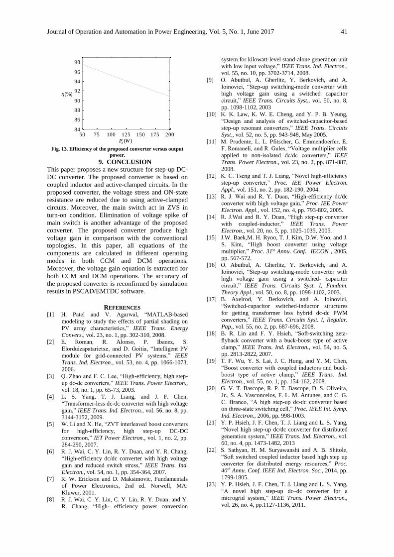
Figure 13 illustrates the proposed converter
efficiency curve, which shows that the maximum
efficiency is 97.8% at a light-load (50W) operation,
and the full load efficiency is about 90.2%.
Table 2. Used parameters in simulation.
Sign Parameter Value
sf Switching frequency kHz50
2C Capacitor with 200V F22
3C Capacitor with 200V F22
oC Output capacitor with
450V F180
mL Magnetizing inductance F48
KL Leakage inductance F25.0
sp NN / Conversion ratio of
coupling inductor 4:1
D Duty Cycle %5.54
(a)
(b)
(c)
Fig. 10. Operation of clamp circuit, (a) Main switch voltage
gain ( dsV ), (b) clamp capacitor voltage ( ccV ), (c) clamp
capacitor current ( ccI ).
Main : Graphs
0.20000 0.20002 0.20004 0.20006 0.20008 ...
...
...
-10
0
10
20
y
ICC [A]
Time[sec]
Main : Graphs
0.20000 0.20002 0.20004 0.20006 0.20008 ...
...
...
90
100
y
VCc [V]
Time[sec]
Main : Graphs
0.20000 0.20002 0.20004 0.20006 0.20008 ...
...
...
0
20
40
60
80
100
120
y
Vds [V]
Time[sec]

E. Babaei et al.: A Developed Structure of Step-Up DC/DC Converter by Using Coupled … 40
(a)
(b)
(c)
(d)
(e)
(f)
Fig. 11. (a) Output voltage ( oV ), (b) leakage inductance
current( LKI ), (c) diode current D2I , (d) diode voltage
( D2V ), (e) output diode current( DoI ), (f) output diode voltage
( DoV ).
(a)
(b)
(c)
Fig. 12. (a) Clamped switch voltage ( ScV ), (b) Main switch
current ( SI ), (c) Clamped switch current ScI .
Main : Graphs
0.20000 0.20002 0.20004 0.20006 0.20008 ...
...
...
0.0
5.0
10.0
15.0
20.0
y
ISc [A]
Time[sec]
Main : Graphs
0.20000 0.20002 0.20004 0.20006 0.20008 ...
...
...
0
10
20
30
40
y
IS [A]
Time[sec]
Main : Graphs
0.20000 0.20002 0.20004 0.20006 0.20008 ...
...
...
0
20
40
60
80
100
120 y
VSc [V]
Time[sec]
Main : Graphs
0.20000 0.20002 0.20004 0.20006 0.20008 ...
...
...
0
50
100
150
200
y
VDo [V]
Time[sec]
Main : Graphs
0.20000 0.20002 0.20004 0.20006 0.20008 ...
...
...
0.0
2.0
4.0
6.0
8.0
y
IDo [A]
Time[sec]
Main : Graphs
0.20000 0.20002 0.20004 0.20006 0.20008 ...
...
...
0
50
100
150
200
y
VD2 [V]
Time[sec]
Main : Graphs
0.20000 0.20002 0.20004 0.20006 0.20008 ...
...
...
0.0
1.0
2.0
3.0
4.0
y
ID2 [A]
Time[sec]
Main : Graphs
0.20000 0.20002 0.20004 0.20006 0.20008 ...
...
...
-10
0
10
20
30
y
ILk [A]
Time[sec]
Main : Graphs
0.20000 0.20002 0.20004 0.20006 0.20008 ...
...
...
373.10
373.20
373.30
373.40
y
Vo [V]
Time[sec]
Journal of Operation and Automation in Power Engineering, Vol. 5, No. 1, June 2017 41
Fig. 13. Efficiency of the proposed converter versus output
power.
9. CONCLUSION
This paper proposes a new structure for step-up DC-
DC converter. The proposed converter is based on
coupled inductor and active-clamped circuits. In the
proposed converter, the voltage stress and ON-state
resistance are reduced due to using active-clamped
circuits. Moreover, the main switch act in ZVS in
turn-on condition. Elimination of voltage spike of
main switch is another advantage of the proposed
converter. The proposed converter produce high
voltage gain in comparison with the conventional
topologies. In this paper, all equations of the
components are calculated in different operating
modes in both CCM and DCM operations.
Moreover, the voltage gain equation is extracted for
both CCM and DCM operations. The accuracy of
the proposed converter is reconfirmed by simulation
results in PSCAD/EMTDC software.
REFERENCES
[1] H. Patel and V. Agarwal, “MATLAB-based
modeling to study the effects of partial shading on
PV array characteristics,” IEEE Trans. Energy
Convers., vol. 23, no. 1, pp. 302-310, 2008.
[2] E. Roman, R. Alonso, P. Ibanez, S.
Elorduizapatarietxe, and D. Goitia, “Intelligent PV
module for grid-connected PV systems,” IEEE
Trans. Ind. Electron., vol. 53, no. 4, pp. 1066-1073,
2006.
[3] Q. Zhao and F. C. Lee, “High-efficiency, high step-
up dc-dc converters,” IEEE Trans. Power Electron.,
vol. 18, no. 1, pp. 65-73, 2003.
[4] L. S. Yang, T. J. Liang, and J. F. Chen,
“Transformer-less dc-dc converter with high voltage
gain,” IEEE Trans. Ind. Electron., vol. 56, no. 8, pp.
3144-3152, 2009.
[5] W. Li and X. He, “ZVT interleaved boost converters
for high-efficiency, high step-up DC-DC
conversion,” IET Power Electron., vol. 1, no. 2, pp.
284-290, 2007.
[6] R. J. Wai, C. Y. Lin, R. Y. Duan, and Y. R. Chang,
“High-efficiency dc/dc converter with high voltage
gain and reduced switch stress,” IEEE Trans. Ind.
Electron., vol. 54, no. 1, pp. 354-364, 2007.
[7] R. W. Erickson and D. Maksimovic, Fundamentals
of Power Electronics, 2nd ed. Norwell, MA:
Kluwer, 2001.
[8] R. J. Wai, C. Y. Lin, C. Y. Lin, R. Y. Duan, and Y.
R. Chang, “High- efficiency power conversion
system for kilowatt-level stand-alone generation unit
with low input voltage,” IEEE Trans. Ind. Electron.,
vol. 55, no. 10, pp. 3702-3714, 2008.
[9] O. Abutbul, A. Gherlitz, Y. Berkovich, and A.
Ioinovici, “Step-up switching-mode converter with
high voltage gain using a switched capacitor
circuit,” IEEE Trans. Circuits Syst., vol. 50, no. 8,
pp. 1098-1102, 2003 [10] K. K. Law, K. W. E. Cheng, and Y. P. B. Yeung,
“Design and analysis of switched-capacitor-based
step-up resonant converters,” IEEE Trans. Circuits
Syst., vol. 52, no. 5, pp. 943-948, May 2005.
[11] M. Prudente, L. L. Pfitscher, G. Emmendoerfer, E.
F. Romaneli, and R. Gules, “Voltage multiplier cells
applied to non-isolated dc/dc converters,” IEEE
Trans. Power Electron., vol. 23, no. 2, pp. 871-887,
2008.
[12] K. C. Tseng and T. J. Liang, “Novel high-efficiency
step-up converter,” Proc. IEE Power Electron.
Appl., vol. 151, no. 2, pp. 182-190, 2004. [13] R. J. Wai and R. Y. Duan, “High-efficiency dc/dc
converter with high voltage gain,” Proc. IEE Power
Electron. Appl., vol. 152, no. 4, pp. 793-802, 2005. [14] R. J.Wai and R. Y. Duan, “High step-up converter
with coupled-inductor,” IEEE Trans. Power
Electron., vol. 20, no. 5, pp. 1025-1035, 2005.
[15] J.W. Baek,M. H. Ryoo, T. J. Kim, D.W. Yoo, and J.
S. Kim, “High boost converter using voltage
multiplier,” Proc. 31st Annu. Conf. IECON , 2005,
pp. 567-572. [16] O. Abutbul, A. Gherlitz, Y. Berkovich, and A.
Ioinovici, “Step-up switching-mode converter with
high voltage gain using a switched- capacitor
circuit,” IEEE Trans. Circuits Syst. I, Fundam.
Theory Appl., vol. 50, no. 8, pp. 1098-1102, 2003.
[17] B. Axelrod, Y. Berkovich, and A. Ioinovici,
“Switched-capacitor switched-inductor structures
for getting transformer less hybrid dc-dc PWM
converters,” IEEE Trans. Circuits Syst. I, Regular.
Pap., vol. 55, no. 2, pp. 687-696, 2008.
[18] B. R. Lin and F. Y. Hsieh, “Soft-switching zeta-
flyback converter with a buck-boost type of active
clamp,” IEEE Trans. Ind. Electron., vol. 54, no. 5,
pp. 2813-2822, 2007.
[19] T. F. Wu, Y. S. Lai, J. C. Hung, and Y. M. Chen,
“Boost converter with coupled inductors and buck-
boost type of active clamp,” IEEE Trans. Ind.
Electron., vol. 55, no. 1, pp. 154-162, 2008.
[20] G. V. T. Bascope, R. P. T. Bascope, D. S. Oliveira,
Jr., S. A. Vasconcelos, F. L. M. Antunes, and C. G.
C. Branco, “A high step-up dc-dc converter based
on three-state switching cell,” Proc. IEEE Int. Symp.
Ind. Electron., 2006, pp. 998-1003.
[21] Y. P. Hsieh, J. F. Chen, T. J. Liang and L. S. Yang,
“Novel high step-up dc/dc converter for distributed
generation system,” IEEE Trans. Ind. Electron., vol.
60, no. 4, pp. 1473-1482, 2013
[22] S. Sathyan, H. M. Suryawanshi and A. B. Shitole,
“Soft switched coupled inductor based high step up
converter for distributed energy resources,” Proc.
40th Annu. Conf. IEEE Ind. Electron. Soc., 2014, pp.
1799-1805.
[23] Y. P. Hsieh, J. F. Chen, T. J. Liang and L. S. Yang,
“A novel high step-up dc–dc converter for a
microgrid system,” IEEE Trans. Power Electron.,
vol. 26, no. 4, pp.1127-1136, 2011.
50 75 100 125 150 175 20084
86
88
90
92
94
96
98
(%)
( )oP W
E. Babaei et al.: A Developed Structure of Step-Up DC/DC Converter by Using Coupled … 42
[24] Y. Zhao, W. Li, X. He, “Single-phase improved
active clamp coupled-inductor-based converter with
extended voltage doubler cell,” IEEE Trans. Power
Electron., vol. 27, no. 6, pp. 2869-2878, 2012.
[25] M. Kim, and S. Choi, “A fully soft-switched single
switch isolated isolated dc/dc converter,” IEEE
Trans. Power Electron., vol.30, no. 9, pp. 4883-
4890, 2015.
[26] S. M. Chen, M. L. Lao, Y. H. Hsieh, T. J. Liang, and
K. H. Chen, “A novel switched-coupled-inductor
dc/dc step-up converter and its derivatives,” IEEE
Trans. Ind. Appl., vol. 51, no. 1, pp. 309-314, 2015.