a depolarizing chipless rfid tag for robust detection and its fcc compliant uwb reading system
TRANSCRIPT
2982 IEEE TRANSACTIONS ON MICROWAVE THEORY AND TECHNIQUES, VOL. 61, NO. 8, AUGUST 2013
A Depolarizing Chipless RFID Tag for RobustDetection and Its FCC Compliant
UWB Reading SystemArnaud Vena, Member, IEEE, Etienne Perret, Member, IEEE, and Smail Tedjni, Senior Member, IEEE
Abstract—A new chipless RF identification (RFID) tag design ispresented in this paper to ease the detection of items in a real envi-ronment. For this purpose, we present multiple scatterers able todepolarize the incident wave to create a response in the orthogonalpolarization. Measurements in anechoic chamber and in a real en-vironment, when the tags are positioned on dielectric and metalobjects, show their higher detection capability. For the first time, astudy on the technique to increase the detection area with a simpli-fied calibration step is carried out. This makes possible the detec-tion of the tag on objects of various sizes and compositions, whichis required in the majority of RFID applications.
Index Terms—Chipless RF identification (RFID), cross-polariza-tion, depolarizing, detection reliability, Federal CommunicationsCommission (FCC) compliant, RFID, ultra-wideband (UWB)reader.
I. INTRODUCTION
R F identification (RFID) is a major technology of iden-tification (ID) that takes its origin during World War II
as the first system to recognize friend or foe aircrafts calledidentification friend or foe (IFF) [1]. Thereafter, RFID was em-ployed for many civil ID systems as an automatic enabling tech-nology. The most known are transportation, pallet tracking, an-imal ID, passports, or antithief systems [2]. However, at theitem tracking level, the optical barcode is still preferred mainlybecause this technology is well established in the worldwidefood supply chain for several decades. To dethrone this agedtechnology, the RFID provide strong improvements. One of themain drawbacks of conventional RFID is the relative high costof the tags. Furthermore, the decision makers of the food supplychain refuse to invest much money in renewing their ID system.To overcome the cost issue of conventional tags, the recent chip-less RFID technology is really promising. Contrary to a con-ventional RFID tag, a chipless tag needs neither a chip inte-grated circuit (IC), nor self or remote empowerment. Thus, notransmission protocol needs to be used for the sake of detec-tion. Instead, a chipless tag may be considered as a radar target
Manuscript received January 05, 2013; revised May 20, 2013; accepted May23, 2013. Date of publication June 21, 2013; date of current version August 02,2013. This work was supported by the French National Research Agency underthe ANR-09-VERS-013 Program References.The authors are with the Laboratoire de Conception et d’Intégration des Sys-
tèmes (LCIS)/Grenoble Institute of Technology, Valence 26000, France (e-mail:[email protected]; [email protected];[email protected]).Color versions of one or more of the figures in this paper are available online
at http://ieeexplore.ieee.org.Digital Object Identifier 10.1109/TMTT.2013.2267748
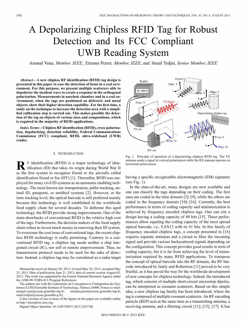
Fig. 1. Principle of operation of a depolarizing chipless RFID tag. The TXantenna sends a signal in vertical polarization while the RX antenna operates inhorizontal polarization.
having a specific recognizable electromagnetic (EM) signature(see Fig. 1).In the state-of-the-art, many designs are now available and
one can classify the tags depending on their coding. The firstones are coded in the time domain [3]–[9], while the others arecoded in the frequency domain [10]–[16]. Currently, the bestperformance in terms of coding capacity and miniaturization isachieved by frequency encoded chipless tags. One can cite adesign having a coding capacity of 49 bits [15]. These perfor-mances allow equaling the coding capacity of the most spreadoptical barcode, i.e., EAN13 with its 41 bits. In this family offrequency encoded chipless tags, a concept presented in [16]requires separate antennas and a circuit to filter the incomingsignal and provide various backscattered signals depending onthe configuration. This concept provides good results in term ofcoding capacity, but it is far from achieving the level of minia-turization required by many RFID applications. To transposethe concept of optical barcode into the RF domain, the RF bar-code introduced by Jalaly and Robertson [11] proved to be veryfruitful, as it has paved the way for the worldwide developmentof new concepts for chipless technology. Indeed, the introducedtag, which consists of multiple short-circuit microstrip dipoles,can be interpreted as resonant scatterers. Based on this simpleidea, a new chipless tag family has been introduced, where thetag is composed of multiple resonant scatterers. An RF encodingparticle (REP) acts at the same time as a transmitting antenna, areceiving antenna, and a filtering circuit [11]; [15]; [17]. It has
0018-9480/$31.00 © 2013 IEEE

VENA et al.: DEPOLARIZING CHIPLESS RFID TAG FOR ROBUST DETECTION AND ITS FCC COMPLIANT UWB READING SYSTEM 2983
already been proven that a really good surface coding efficiencycan be achieved with such a kind of chipless tag. Moreover, aground plane is not always needed, so this eases the realization.However, the next stage before the final acceptance of the
chipless technology and more precisely the REP approach is tomake it more reliable and realistic in case of a real application.This paper focuses on this issue and presents a new design
that can be read in a practical environment. This means for var-ious and unknown items, within a large zone of detection andwith a unique calibration process. The major improvement hereis to use depolarizing REPs. A depolarizing tag reflects part ofits EM signature in the cross-polarization compared to the inter-rogating pulse (see Fig. 1). The aim is to obtain a chipless tagreliable in detection while keeping a reduced size compared toprevious design in [16].In Section II, basic principles of chipless RFID tags and
systems are presented. The design of a depolarizing tag isdiscussed. In Section III, measurement setup and results ob-tained in an anechoic chamber and in a real environment areshown. Finally, in Section IV, we present the result obtainedwith commercial ultra-wideband (UWB) radar compatiblewith the power mask defined by the Federal CommunicationsCommission (FCC).
II. BASIC PRINCIPLE
A. Scattering
As previously said, a chipless tag can be seen as a radar targetthat reflects part of the incident signal with its specific signa-ture. The phenomenon can be resumed in several steps in caseof a tag based on multiple REPs. The incident EM wave im-pinges the conductive strips of the tag. This creates some sur-face currents on the strips. First, the main part of the energy isdirectly reflected by the structure in a quasi-optical way. This isthe early time response. Depending on the geometry, a standingwave mode can be created so that a resonant behavior may ap-pear. In this case, the signature is spread over the time and ismade of a summation of damped sinusoids.The EM response of a tag is generally dependent on the polar-
ization of the incident wave as well as its direction. Usual tagsare composed of REPs that reflect the energy only in co-polar-ization [12]; [14]; [15]; [18]. However, some are able to sharethe reflected energy in co-polarization and in cross-polarizationby using two different antennas [16]; [19]. It will be shown laterin this paper that the second ones provide a better detection re-liability.The polarization of the reflected wave is related to the orien-
tation of the current paths on the conductors of the resonator.In most of the scatterers, the surface currents on the metal ele-ments generate only a reflected wave in the polarization of theincident signal. This is particularly the case for a right shorteddipole [11], a C-like resonator [13], a circular [15], or rectan-gular ring. To enable the generation of a signal in a polarizationother than the polarization of the incident wave, it is necessary tocreate an asymmetry in the resonator geometry. In Fig. 2(a) and(b), we propose two structures with a ground plane composed ofresonators allowing a response in cross-polarization. These twodesigns will be measured and compared in Section II-B. The
Fig. 2. (a) Tag based on dual-L resonators. Dimensions of this tag (tag 1) aregiven in Table I. (b) Tag based on shorted dipoles oriented at 45 . Dimensionsof this tag (tag 1) are given in Table II.
idea in this paper is to show that several elementary resonatorsare able to reflect a response in cross-polarization. The choiceof the geometry is critical because it affects the RCS and the se-lectivity. The first structure uses resonators whose geometry isbased on the combination of two inverted L [see Fig. 2(a)]. Theresonators of the second structure shown in Fig. 2(b) are com-posed of multiple coupled shorted dipoles, and oriented at 45 .When impinged by a vertically polarized plane wave, the
dual-L resonator of Fig. 2(a) generates surface currents that willmove from bottom to top and from left to right or vice versa, asshown in Fig. 3(a). A horizontal component appears and willtherefore generate an EM signature in cross-polarization. Theresonator backscatters a portion of the energy in vertical po-larization (V) and another part in horizontal polarization (H).In Fig. 3(b), one can see the response in co-polarization (VV)shows dips in the spectrum at resonant frequencies. The dipsare due to a destructive interference between the resonant scat-terers and the rectangular shaped ground plane, which generatean UWB response. In the cross-polarized response (VH), onlypeaks due to the resonant scatterers can be observed. In this case,the ground plane, like most ordinary objects, does not depolarizethe incident wave and therefore cannot interfere with the reso-nant mode.The use of two inverted L’s instead of one increases the level
of the radar cross section. The gap between the two L’s mainlyaffects the resonant frequency. A small value tends to shift thepeak to a lower frequency. The strip width is correlated with

2984 IEEE TRANSACTIONS ON MICROWAVE THEORY AND TECHNIQUES, VOL. 61, NO. 8, AUGUST 2013
Fig. 3. (a) and (b) Tag REP based on dual-L resonators. (a) Surface currentdensity at resonance. (b) Simulated RCS response in co-polarization (VV) andin cross-polarization (VH). The tag dimensions are mm and
mm. (c) and (d) Tag REP based 45 shorted dipoles. (c) Surface currentdensity at resonance. (d) Simulated RCS response in co-polarization (VV) andin cross-polarization (VH). The tag dimensions are mm, mm,and mm.
the RCS peak value. A large width is beneficial to maximizethe RCS. However, to keep a compact size, we found that awidth mm at 4 GHz is a good tradeoff. The resonantfrequency of the scatterer is mainly controlled by the length[see Fig. 3(a)]. A single REP has been optimized at 4 GHz thatis the starting operating frequency chosen for this design. Tomodify the resonant frequency while keeping a good selectivity,a scaling factor is applied on the optimized REP. The result ofa parametric study based on the variation of this scaling factoris provided in Fig. 4(a). The curves show both the frequency ofthe first resonant mode and the 3-dB bandwidth around the peakas a function of a scaling factor between 1–0.5.The radiating of 45 shorted dipoles is very close to the
dual-L resonator. Similarly, when a vertically polarized inci-dent wave impinges the resonator, the current is guided alongthe dipoles. Since these dipoles are oriented at 45 , a horizontalcomponent is created generating a response in cross-polar-ization [see Fig. 3(c)]. As for the REPs based on dual-L, weobserve a dip in co-polarization and a peak in cross-polarizationat resonance frequency [see Fig. 3(d)]. When using severaldipoles of the same length, the level of response increaseswhile keeping a good selectivity. If dipoles are close, we cancontrol both the width and the gap between them to convergeto an optimized REP. We observed that a large strip widthmaximize the magnitude of the resonant peak, and decreasesthe value of its frequency. A strip width mm is onceagain a good tradeoff between a large RCS and a compact de-sign. Concerning the separation between dipoles, we did notobserve a strong influence on the key parameters (frequency,selectivity, RCS), hence, in order to get a compact REP, wechose a small value mm, but easy to achieve with a
Fig. 4. (a) Frequency and bandwidth at resonance as a function of the scalingfactor for a dual-L based REP ( mm, mm, mm).(b) Frequency and bandwidth at resonance as a function of the length for aoriented dipole based REP ( mm, mm).
chemical etching realization process. The resonant frequencyof the resonators is determined by the length of the dipoles.Fig. 4(b) presents the result of a parametric study related to thelength of the REP shown in Fig. 3(c). One can see that thebandwidth of the oriented dipole based REP is larger than theone obtained with the dual-L based REP for a given frequency.However, the RCS is higher.It is noteworthy that for the two REPs introduced, the de-
polarization effect can be observed only for four orientations,which are 0 , 90 , 180 , and 270 . Thus, it means that, as formost chipless tag designs, this design is polarization dependent.To gain in flexibility, and make it work whatever the orientationof the tag, the reading system needs polarization agility.
B. Model of the Detection System
To better understand why tags generating a response in cross-polarization provide a higher reliability, a model of the detec-tion system is proposed in Fig. 5. Indeed, this channel model ofa radar system introduced in [20] may also be used for a chip-less RFID system. Compared to [20], an additional block func-tion has been added to represent the effect of various unknownobjects, such as the cardboard on which the tag is applied. Inthis model, each block is a 2 2 -matrix containing four scat-tering terms. Two terms represent the co-polarization transfer

VENA et al.: DEPOLARIZING CHIPLESS RFID TAG FOR ROBUST DETECTION AND ITS FCC COMPLIANT UWB READING SYSTEM 2985
Fig. 5. Channel model of the detection system. The chipless tag ( ) and thesum of unknown objects ( ) both contribute to the total scattered field.
function, while the two others define the behavior in cross-po-larization. The inputs and the outputs of eachblock function are defined like root power or voltage waves inthe two polarizations (vertical and horizontal).The RF frontend or the chipless RFID reader is represented
by the block denoted by . The transmit path and the re-ceive path represent cables and antennas. If neither tag ,nor objects are in the front of the antennas, the measurementrecords the effect of direct coupling between antennas, also
called isolation measurement, referred to as in (1). Thus, whena chipless tag and others objects are in the detection areaaccording to the Fig. 5, the measurement result may be writtenas in (2) and a matrix form is given in (3) as follows:
(1)
(2)
(3)
When a chipless tag is detected in co-polarization accordingto the vertical polarization, we derive the term to obtain(4) as follows:
(4)
Similarly, in cross-polarization (VH), the term may beextracted from (3), shown in (5) as follows:
(5)
In an usual case, the surrounding objects in the detection area,including the object on which the tag is applied, do not de-po-larize so that their cross-polarization terms ( and ) canbe considered as to be null. In this case, one can rewrite (4) and(5), respectively, into (6) and (7) as follows:
(6)
(7)
In a detection system sensitive to the cross-polarization, theantennas are chosen so that the isolation between the co-polar-ization and the cross-polarization is the highest possible. Typ-ical values are 20 dB for a dual polarization antenna. This meansthat the terms , , , and are relatively low com-pared to the co-polarization terms denoted , , , and
. In common cases, when the unknown object to detectdoes not have a very large EM response in co-polarization (and ), we can consider the products in (6) lowenough to be neglected, to compare with the others terms (theresult of the product is attenuated by 40 dB). Also, the terms
and in (7) are not significant enoughto compare with the term so they can be neglectedas well (the result of the product andare and , respectively, attenuated by 20 dB). Inthis particular case, (6) and (7) may be approximated by (8) and(9),
(8)
(9)
(10)
--
(11)
-- (12)
Equation (10) derived from (9) allows extracting the cross-polarization term of the chipless tag response . For this pur-pose, a first measurement of the empty environment is neces-sary to determine the isolation . The measurement of a refer-ence target is then - . Having a known response, - ,is necessary to determine the couple due to the filteringeffect of the transmitting and the receiving antennas (11). Fi-nally, one can obtain (12) using (10) and (11) in order to extractthe cross-polarization scattering term of a chipless tag with threemeasurement results, which are , , and - .In (8), one can remark that there is a term due to the echoes
of surrounding objects in co-polarization. This term is usuallymuch larger than the response of the tag so that it becomes im-possible to extract the tag response if the surroundingobjectsare unknown. Indeed,with the calibration technique alreadyusedin [15] and [21] and the corresponding (8), the co-polarizationterm can be extracted only for a given object recorded at

2986 IEEE TRANSACTIONS ON MICROWAVE THEORY AND TECHNIQUES, VOL. 61, NO. 8, AUGUST 2013
a given distance. If the object moves, the calibration is not validanymore. On the contrary, in (9), corresponding to the cross-po-larization response, there is no term due to surrounding objectsso that if the object moves and its positioning (within a detectionarea located in front of the radar’s antennas) does not modify thecalculated extracted term because in cross-polarization, thecalibration does not depend on the object EM signature. This re-sult is very important because this means that a tag generating aresponse in cross-polarization is detectable in a real environmentcontainingunknownobjectswith thehelpof aunique calibration.This assumption will be validated in Section III by several mea-surementswithhighlyreflectiveunknownobjects (metal,water).
C. Final Tag Design and Coding Technique
Before making a complete tag, the coding technique has to bechosen. For chipless tags operating in the frequency domain, wehave the choice to use an absence/presence technique in whichone bit is associated to one resonator or REP. This techniqueprovides the best density of coding for a given frequency band(in bits/GHz). However, the density of coding per surface unit(in bits cm ) is very low [22]. Moreover, this technique is gen-erally preferred for single-layer chipless tags that are muchmoresensitive to the detuning effect of the carrier than for groundedtags. Besides, another technique called the frequency shift tech-nique [13] provides the best surface density of coding so thatnumerous bits can be obtained with a few REPs. This dramati-cally decreases the tag surface. In case of single-layer chiplesstags, this coding technique suffers from the detuning effect ofthe container. However, recently it was demonstrated that usingone [21] or more [14] sensing REPs makes it is possible to com-pensate the undesired frequency deviation. Thus, the right iden-tifier can be detected for various unknown objects. For all thesereasons, we decided to encode the ID of the presented tags usingthis last technique.The two tag designs presented in Fig. 2(a) and (b) have been
optimized based on the following criteria: frequency (centeredwith respect to the bandwidth of interest), the selectivity thatis the 3-dB bandwidth of the peak, and the level of responsein the preferred direction. The level or response has to be maxi-mized because it is correlated with the detection range of the tag.Further, the 3-dB bandwidth has to be as narrow as possible tomaximize the coding capacity according to the coding schemeused [13]. The tags have been realized by chemical etching ofcopper on an RO4003 substrate having a permittivity of 3.55 anda . Indeed, using a low-loss substrate is manda-tory for grounded REPs to generate peaks or dips having a goodselectivity.Regarding the tag based on the dual-L of Fig. 2(a), a single
REP has been optimized at 4 GHz giving specific dimensions.To create a REP operating at other frequencies, we then applya magnification/reduction of the surface geometry giving acouple of parameters and , according to the parametricstudy given in Fig. 4(a). Concerning the tag based on orientedshorted dipoles, the resonant frequency of a single REP isdetermined by its length [see Fig. 4(b)]. Unlike the dual-LREP, to maintain a high level of RCS, the width of the dipolesor their separations are not modified.
TABLE IDIMENSIONS IN MILLIMETERS OF REPs FOR TAGBASED ON DUAL-L RESONATORS ( mm)
TABLE IIDIMENSIONS IN MILLIMETERS OF REPs TAG BASED ON SHORTED DIPOLESORIENTED AT 45 ( mm, mm, mm, mm)
The dimensions of each REP are given for several tag con-figurations in Tables I and II, respectively, for the tag basedon dual-L and for the tag having oriented shorted dipoles.Based on the selectivity that can be achieved, a resolutionfrequency of MHz is chosen for these designs. Forthe dual-L resonator, an operating bandwidth of 3 GHz between4–7 GHz is chosen. Within this band, resonant peaks aredistributed. Thus, each resonant peak has a frequency span of
MHz in which it can be shifted. Equation (13)[22]is useful to calculate the total coding capacity of a tag basedon frequency shift encoding. One can findcombinations, i.e., 14 bits. For this design, three configurationshave been realized to get three different IDs. Based on thedimensions of each REP, tag 1 encodes the ID “100000,”whereas tags 2 and 3 encode, respectively, the IDs “011111”and “202120.” Concretely, this means that from tag 1 to tag 2,the first resonant peak is shifted back to the lowest frequency,whereas the other modes are shifted to higher frequency values.For tag 3, every peak is shifted to higher frequencies, exceptthe numbers 2 and 6,
(13)
For the tag based on oriented shorted dipoles, a larger op-erating bandwidth can be used because the second resonancemode has a resonant frequency three times greater than that ofthe first mode. To compare, the tag based on dual-L has a secondresonant mode at two times the resonant frequency of the firstmode. Similarly, using (13), one can calculate the coding ca-pacity for resonant peaks distributed within a frequency

VENA et al.: DEPOLARIZING CHIPLESS RFID TAG FOR ROBUST DETECTION AND ITS FCC COMPLIANT UWB READING SYSTEM 2987
bandwidth of 4 GHz between 3–7 GHz. Thus, here again a fre-quency span MHz is available for each resonantpeak. This provides a number of combinations
, i.e., 18.5 bits. The parameters of the three configura-tions realized for this second design are provided in Table II. Inthis case, from tag 1 to tags 2 and 3, only the first resonant peak isshifted so that the generated IDs are, respectively, “00000000,”“10000000,” and “20000000” for tags 1–3.The measured EM responses corresponding to these different
configurations are provided in Fig. 7(a) and (b) for the two de-signs.
III. MEASUREMENT
Unlike an anechoic environment, in the real environment thefollowing effects will interfere, and more often, degrade themeasurement:• the reflection of surrounding objects that may interferewith the response of the tag;
• the multipaths;• the wireless communications in the UHF band (900 MHz,2.45 GHz) and SHF (5.8 GHz), including the GSM net-work and the Wi-Fi network everywhere in the building.
Let us consider that surrounding objects are not mobile so thecluttermapdoesnotvaryover time. It isnoteworthythat theobjecton which the chipless tag is applied is not included in the sur-rounding objects because it can bemobile. Information about thedetection environment is gathered by measuring it without anytags.The multipath signals are related to the reflections of the tag
response on surrounding objects, and will be added to the firsttransient response received by the detection system. Fromaprac-tical point of view, the effect will tend to discretize the frequencyresponse of the tag. Tomitigate this effect, a timewindow can beused tokeeponly thefirst transient response received.Finally, wireless communications, which are ubiquitous in
real environment, may interfere with certain frequencies ofchipless tags, including 2.45 and 5.8 GHz. These communica-tions will vary with time and are therefore uncorrelated withthe tag response that remains the same over time. By applyingan averaging technique on several measures, in the same wayas for mitigating the white noise, the effect of the wirelesscommunications will be damped.We used the frequency measurement setup, previously intro-
duced in [21]. Photographs of the measurement environmentfor the tag alone and the tag placed on a cardboard are pre-sented, respectively, in Fig. 6(a) and (b). The room used forthe measurement contains tables, chairs, and many metal ele-ments. The antenna used is a SATIMOQH2000 (open boundarywideband quad ridge antenna) dual polarization that operatesin the 2–32-GHz band. Its gain is between 6–11 dBi between2–10 GHz. We therefore use a mono-static radar configurationbecause the source and the receiver are collocated. Port 1 ofthe VNA is connected to the vertical polarization antenna port(bottom connector) for excitation, while port 2 is connected tothe horizontal polarization antenna port for receiving (connectoron the side). The -parameter at the VNA provides the tag re-sponse in cross-polarization (VH), while the -parameter isused to measure the response in co-polarization (VV).
Fig. 6. (a) Photograph of depolarizing tag based on shorted dipole at 10 cmfrom the antenna. (b) Photograph of the tag based C-like resonator placed ona cardboard filled with paper sheets. The antenna used is a dual polarizationSATIMO QH 2000 operating between 2–32 GHz.
Fig. 7. Cross-polarization measurements for de-polarizing tags based on:(a) 45 shorted dipoles having the dimensions given in Table II. (b) Dual-Lresonators having the dimensions given in Table I. The results presentedare obtained by simply subtracting the measurement of the tags with themeasurement of the empty environment.
A. Free-Space Detection
As we can see in Fig. 6(b), the antenna is directed towarda plaster wall of small thickness separating the measurementroom from another office. The first measurements are madewhen the tags are placed on a plastic substrate [see Fig. 6(a)],whose influence on the EM response is very low. The results ob-tained are presented in Fig. 8(a) and (b) for a detection distanceof 10 cm and a transmit power of 0 dBm.

2988 IEEE TRANSACTIONS ON MICROWAVE THEORY AND TECHNIQUES, VOL. 61, NO. 8, AUGUST 2013
Fig. 8. (a) and (b) Cross-polarization (VH) results for tag 1 based on shorted dipoles [see Fig. 6(b)], measured at several distances on a box of paper sheets: (a) inthe ideal case and (b) in a more practical configuration. (c) and (d) Co-polarization (VV) results for the tag based on C-like resonators [21] measured at severaldistances on a box of paper sheets: (c) in the ideal case and (d) in a more practical configuration. (e) and (f) Measured EM responses of the box of paper sheets atseveral distances subtracted from the empty environment response: (e) in cross-polarization (VH) and (f) in co-polarization (VV).
These curves are obtained by subtracting the measurementsof tags from the empty measurement. It is important to noticethat, in such a case, a calibration procedure using a reference ob-ject as described above is not necessary to find the ID of the tag.This means that the receiver of the detection system does notchange the shape of the reflected signal too drastically. How-ever, for coding techniques tracking very small changes in am-plitude or phase of the reflected signal, the calibration proceduredescribed in Section II can be required. An averaging based onten measurements allows for the increase of the signal-to-noiseratio (SNR). As stated earlier, this operation is not necessaryin anechoic environment. The curves shown Fig. 8(a) and (b),respectively, shows the response of depolarizing tags based onshorted dipoles and the tags based on dual-L for different con-figurations.All the peaks can be clearly observed. The frequency shift
from one configuration to another can be detected without anyerror, according to the tag’s code given in Tables I and II. Inthis case, we noticed no degradation compared to an anechoicenvironment.
B. Detection on Low-Permittivity Objects
To be closer to a practical application, we also perform mea-surements when the tags are positioned on a box filled withpaper, as shown in Fig. 6(b). Thus, here we try to identify a
large object compared to the tag dimensions. The object reflectsan EM flat response with a magnitude 10 dB greater than the tagand even more.It is to be noted that the EM magnitude response of the object
and the tag are very sensitive to the detection distance. Thus, thecalibration technique based on three measurements, previouslydescribed, will work only for a unique distance. To prove thereliability of the tag based depolarizing REP, i.e., to prove thatthese tags can be read whatever the distance be, we present twodifferent scenarios: the ideal and the practice case. Regardingthe ideal case, we consider that the cardboard on which the tagis placed belongs to the empty environment. This means that allthe calibration measurements (for instance, whatever the dis-tance) are done with the cardboard. Second, in a more realisticcase, the object to identify is considered to be unknown so thecalibration measurements must be done without any cardboard.In the ideal case, we measure the response of the environment
containing the cardboard at several distances, from 10 to 20 cm,and remove it from the tag response, which gives the curves inFig. 8(a). We can observe that whatever the distance of the tag,the resonance peaks are distinguishable in all cases.In the more practical configuration, it is required that any un-
known object of variable dimensions be detected at various po-sitions. Thus, the signature of the cardboard cannot be takeninto account in the calibration. Indeed, the isolation measure-ment, denoted as in (1), does not contain the huge signature of

VENA et al.: DEPOLARIZING CHIPLESS RFID TAG FOR ROBUST DETECTION AND ITS FCC COMPLIANT UWB READING SYSTEM 2989
the object. We can only subtract the response of the empty envi-ronment, without any cardboard from the total response of thetag placed on the cardboard. We can see that only one measure-ment is needed for the calibration process while four measure-ments (one for each distance plus the empty environment) wereneeded in the first case. The results are presented in Fig. 8(b).Once again the results are very good and we can extract all theresonant peaks up to 20 cm of reading distance for various lo-cations, keeping the same calibration. This shows a very gooddetection reliability of depolarizing tags. Indeed, the responseof the tag based depolarizing REP is generated both in the ver-tical and horizontal polarization, while the excitation of the tagis performed in the vertical polarization.Due to the variable and large response of the single cardboard
in the co-polarization (VV), a tag based on C-like REPs [21]can be used only in the ideal case; i.e., when the cardboard hasa known geometry and its position is accurately known. Indeed,Fig. 8(c) shows in such a case the measurement results of thetag based on C-like REPs in co-polarization (VV) at variousdistances. The resonant peaks can be distinguished for everydistance. It should be noted that the response in co-polarizationis extracted using the -parameter. In this case, the measuredresponse level is well below the level of reflection due to thesimple mismatch of the antenna.The second scenario for which the response of the cardboard
is not known in advance is the worst case for the tag operatingonly in co-polarization. In Fig. 8(d), the measurement resultswhen the overall response is subtracted from the empty envi-ronment without cardboard are shown for various distances. Inthis case, one can see that it is impossible to distinguish the tagresponse.A usual object like a cardboard does not depolarize so it tends
to reflect the wave only in co-polarization, that is to say, in ver-tical polarization, as explained previously and depicted in Fig. 1.It is quite invisible in cross-polarization that is horizontal in thiscase, andwill not interfere with the response of the tag in this po-larization. Fig. 8(e) and (f), respectively, showing the responseof the cardboard filled with paper in cross-polarization and inco-polarization, confirms this behavior. The response level is al-most constant at 55 dB in cross-polarization close to the isola-tion level of the antenna, while a variable response level around25 dB can be measured in co-polarization. This gives a huge
difference of 30 dB between the two polarizations. Based onthis observation, the theoretical model presented in Section IIand the approximations used can be fully applied in this situ-ation. The cross-polarization measurement contains mainly theEM response tag and the approximation made with the (9) isvalidated.These measurements made in a real environment demonstrate
that it is possible to identify chipless tags in the presence of var-ious sources of interference, such as those typically encounteredin buildings. We show here that a detection of a tag placed on anunknown object (here, a cardboard full of paper) is a reality. Inaddition, through measurements made by varying the detectiondistance, we have shown that depolarizing tags provide muchhigher robustness. They are decisive in practice insofar as iteliminates a large number of calibration measurements, whichmay not be performed in a practical application. In other words,
Fig. 9. Photograph of the tag under test put on: (a) a pack of bottles of waterand (b) a pack of metal coffee cans.
this principle allows decoding the identifier of the tag withoutknowing the object in advance. Moreover, a variation in the po-sitioning of the order of 20 cm does not alter the peak resonance.
C. Detection on Metal and High-Permittivity Objects
According to the encouraging previous results, we studied thedetection of depolarizing tags on high-permittivity and metalobjects. This is the ultimate step to prove the reliability of themethod. We put the tags on a pack of bottle of water and on apack of metal coffee cans, as shown in Fig. 9(a) and (b), respec-tively. The co-polarization and cross-polarization responses ofthe pack of bottle of water and the metal cans are provided inFig. 10 for a separation of 10 cm with the antenna. It confirmsthat even with highly reflective objects, the cross-polarizationresponse level is still much lower (more than 20 dB lower) thanfor the co-polarization response. This value is not really a hazardand is correlated with the cross-polarization isolation of the an-tenna that is close to 20 dB. Thus, in such a case, the cross-polar-ization response is only due to the leakage of the co-polarizationresponse within the antenna.

2990 IEEE TRANSACTIONS ON MICROWAVE THEORY AND TECHNIQUES, VOL. 61, NO. 8, AUGUST 2013
Fig. 10. Measured EM responses of the pack of water bottles and the pack ofmetal coffee cans at 10 cm subtracted from the empty environment response incross-polarization (VH) and in co-polarization (VV).
Fig. 11(a) and (b) shows the measurements results for the de-polarizing tags based on oriented dipoles, put on a pack of waterbottles and on a pack of metal coffee cans, respectively. Thoseresults are extracted with a subtraction of the tagged object, fromthe empty environment with no object in front of the antenna.In both cases, all the resonant peaks can be extracted when thetags are 10 cm away from the antenna. For comparison, the re-sponse of the object alone with no tag is given. We can observe10-dB difference between each peak and the response of the ob-ject alone. For the pack of metal coffee cans, this isolation isless. Thus, the curves are more altered in this case, but all thepeaks are still clearly visible. At 20 cm, we noticed that the tag’sresponse cannot be extracted anymore because the ratio betweenthe tag’s response strength and the tagged object is close to one.The leakage between the two polarizations within the antennais too significant regarding the tag’s signal strength. One meanto improve this read range is to perform the cross-polarizationisolation of the antenna using two separate antennas.
D. Detection Among Depolarizing Objects
To examine the effect of depolarizing objects that may in-terfere with the backscattered response of the chipless tag, weused a single metal coffee box that can rotate from 0 to 90 ,as shown in Fig. 12(a) and (b). The can does not depolarize thewave when the angle is 0 or 90 , whereas the worst case iswhen the can is 45 rotated. We observed for 45 , a responselevel of the can, in cross-polarization, up to 15 dB higher thanthe case 0 or 90 . In Fig. 12(c), we can observe the response ofa depolarizing tag as a function of the rotation angle of the can.Meanwhile, the tag is kept aligned with the antenna, as shown inFig. 12(a). One can see that the largest dynamic of the peaks isobtained for an angle of 90 and 0 . At 45 , the can’s cross-po-larization response reaches its maximum level. However, we arestill able to recognize the eight peaks of the tag with a peak dy-namic that is much lower compared with the case 0 . Thus, this
Fig. 11. Measured EM responses in cross-polarization (VH) subtracted fromthe empty environment response for the oriented dipoles based tags at 10 cmfrom the antenna. (a) On a pack of water bottles and (b) on a pack of metalcoffee cans.
proves that even in the presence of a highly reflective depolar-izing object, the EM signature of the tag is extracted properly.
IV. READING SYSTEM BASED UWB IMPULSE RADAR
Commercial UWB radar systems dedicated for the localiza-tion of objects or people through the walls can be found for acost lower than 10 k$. However, they are not really dedicatedfor ID of chipless RFID tags. For a localization application,only the round-trip time of the emitted pulse is needed con-trary to an ID application that also needs knowing the shapeof the reflected signal. However, some products offer the abilityto record the waveform of the received signal. This is a manda-tory feature to transform localization radar into a chipless RFIDreader. The radar proposed by the company Novelda1 has al-ready been used for the detection of time-coded chipless tag[9]. In the present case, we carry out some experiments to de-tect a frequency-coded chipless tag. The radar is composed ofa CMOS RF front-end mounted on a printed circuit board, as
1[Online]. Available: http://www.novelda.no/

VENA et al.: DEPOLARIZING CHIPLESS RFID TAG FOR ROBUST DETECTION AND ITS FCC COMPLIANT UWB READING SYSTEM 2991
Fig. 12. (a) Description of the measurement setup to observe the effect of adepolarizing object on the response of a depolarizing chipless tag. (b) View ofthe measurement setup. (c) EM response of an oriented dipoles based chiplesstag for various orientation of the metal box in the detection area of chipless tags.
shown in Fig. 13. In the front-end are embedded a pulse gen-erator and a customized equivalent time sampler [23]. On theboard, a microcontroller is used to control the RF front-end andmake the connection with a computer via a serial port.We devel-oped an application in MATLAB to extract and process the rawsignals recorded by the RF front-end. We then replaced the sup-plied antennas with the one used in the earlier measured setup[see Fig. 5(a) and (b)]. The radar is specified to be FCC com-pliant and to operate over a frequency range of 0.45–9.55 GHz,and features a sample rate greater than 30 Gs/s.To verify these characteristics, we recorded the emitted pulse
using a wideband digital sampling oscilloscope (DSO) [seeFig. 14(a)] and directly on the radar by shorting the emitterto the receiver with an attenuator. The frequency response ofthis pulse is shown in Fig. 14(b). According to the frequencyresponse of the recorded pulse by the radar, we can note a3-dB bandwidth equal to 4.5 GHz between 1.5–6 GHz. For7 and 8 GHz, the normalized power spectral density (PSD)is, respectively, equal to 10 and 20 dB so the detectionrange is reduced at these frequencies. The same pulse recordedon the DSO gives a theoretical bandwidth at 3 dB between2.4–6.8 GHz. Thus, this means that the radar receiving stageamplifies the lowest frequencies more. However, it still seemspossible to detect tags between 3–7 GHz. The free-spacemeasurements previously performed with a VNA are now
Fig. 13. Photograph of the Novelda radar [23] connected to test antennas.
Fig. 14. (a) Pulse waveform at the output of the Novelda radar recorded by itsown receiving stage through an attenuator and by a wideband DSO. (b) Nor-malized PSD of the recorded pulse.
performed with the commercial radar. We added a low-noiseamplifier between the receiving antenna and the receiving portof the radar. An averaging operation on 100 measurementsis carried out to increase the SNR. The calibration procedurepreviously described remains the same. One can find (14)to calculate the RCS of tags under test as a function ofthe frequency based on the known RCS of the reference

2992 IEEE TRANSACTIONS ON MICROWAVE THEORY AND TECHNIQUES, VOL. 61, NO. 8, AUGUST 2013
Fig. 15. Measured responses with Novelda radar of depolarizing tagsbased on: (a) 45 shorted dipoles and (b) dual-L.
scatterer. In this equation, , , andare the sampled signals for the tag only, the reference only, andthe background with no object, respectively,
(14)
Fig. 15(a) and (b) shows the measurement results obtained forthe depolarizing tags, respectively, based on shorted dipoles anddual-L. The tags are positioned 20 cm away from the dual polar-ized antenna. In both cases, we clearly see the presence of reso-nant modes depicted by the numbers 1–8 in Fig. 15(a) and 1–6in Fig. 15(b). The usable frequency range starts below 3 GHz tomore than 7 GHz, which is perfectly suited to the detection ofthese tags.According to the tag configurations, only mode 1 is modi-
fied from one configuration to another one. Other modes are notchanged and the curves are quite the same for these frequencies,as expected.To better appreciate the performance of this radar, we super-
imposed the results obtained with the measurement setup based
Fig. 16. Comparison between Novelda (radar) and VNA (freq.) results: (a) fortag based on 45 shorted dipoles and (b) for tag based on dual-L.
VNA and with the Novelda radar. In Fig. 16(a) and (b), wecan compare results, respectively, for tag 2 based 45 shorteddipoles and for tag 1 based on dual-L. One can observe that res-onance peaks are well correlated in both cases. The resonantpeaks are slightly mitigated in case of radar, but in all cases, thepeaks are clearly distinguishable.In case of tag based 45 shorted dipole [see Fig. 16(a)], peaks
of highest frequencies are less selective than for tags based ondual-L [see Fig. 16(a)], but the results obtained with the Noveldaradar are quite similar compared to those obtainedwith the VNAup to 7 GHz.
V. CONCLUSION
We have discussed in this paper a fundamental aspect ofthe development of chipless RFID technology that is practicalimplementation and measurement of tags. Depolarizing tagsshowed their great potential since they allowed detection of thesignature of a tag on various highly reflective objects. Mea-surements in a real environment showed that it was entirelypossible to detect depolarizing chipless tags on a cardboardfilled with paper, as well as on pack of bottles of water and onmetal cans. The EM response of the cardboard and its locationare not necessarily known. This makes it possible to detect thetag on objects of different sizes, within a variable detectionrange, up to 20 cm. For this achievement, only one calibrationis necessary. These results have been performed with a radarmeasurement system based frequency sweep and for a radiating
VENA et al.: DEPOLARIZING CHIPLESS RFID TAG FOR ROBUST DETECTION AND ITS FCC COMPLIANT UWB READING SYSTEM 2993
power of 0 dBm. This result is remarkable and makes thissystem compatible with most of the requirements found in theareas of ID.Since this technology is relatively new and is based on a very
different principle compared to classical modulation schemes,there is no dedicated reader today. To meet the restrictive stan-dards that define UWB transmission power masks, we made thechoice to design an impulse radio detection system. Indeed, sig-nals with low duty cycles make it possible to focus energy on arelatively short time, fully compliant with the standards that de-fine a limit for mean radiated powers. Through the implementa-tion of an UWB impulse radar, normally dedicated for localiza-tion applications, we have shown that it is possible to detect theEM signature of chipless tags with a good correlation comparedto the results obtained with a VNA. Due to the compactness ofthe radar and its relatively low cost (about 2000 € with thelow noise amplifier), these results provide proof of concept of achipless RFID system robust and cheap.
ACKNOWLEDGMENT
The authors are grateful to A. Guillet for his technical help.
REFERENCES
[1] J. Landt, “The history of RFID,” IEEE Potentials, vol. 24, pp. 8–11,2005.
[2] K. Finkenzeller, RFID Handbook: Fundamentals and Applications inContactless Smart Cards, Radio Frequency Identification and Near-Field Communication. New York, NY, USA: Wiley, 2010.
[3] A. Chamarti and K. Varahramyan, “Transmission delay line basedID generation circuit for RFID applications,” IEEE Microw. WirelessCompon. Lett., vol. 16, no. 11, pp. 588–590, Nov. 2006.
[4] C. Hartmann, “A global saw ID tag with large data capacity,” in Proc.IEEE Ultrason. Symp., 2002, pp. 65–69.
[5] C. Mandel, M. Schussler, M. Maasch, and R. Jakoby, “A novel passivephase modulator based on lh delay lines for chipless microwave RFIDapplications,” in IEEE MTT-S Int. Microw. Wireless Sens., Local Posi-tioning, RFID, Workshop, 2009, pp. 1–4.
[6] R. Nair, E. Perret, and S. Tedjini, “Temporal multi-frequency encodingtechnique for chipless RFID applications,” in IEEEMTT-S Int. Microw.Symp. Dig., 2012, pp. 1–3.
[7] S. Shrestha, M. Balachandran, M. Agarwal, V. Phoha, and K.Varahramyan, “A chipless RFID sensor system for cyber centricmonitoring applications,” IEEE Trans. Microw. Theory Techn., vol.57, no. 5, pp. 1303–1309, May 2009.
[8] L. Zheng, S. Rodriguez, L. Zhang, B. Shao, and L. Zheng, “Designand implementation of a fully reconfigurable chipless RFID tag usinginkjet printing technology,” in IEEE Int. Circuits Syst. Symp., 2008, pp.1524–1527.
[9] A. Ramos, D. Girbau, A. Lazaro, and S. Rima, “IR-UWB radar systemand tag design for time-coded chipless RFID,” in EUCAP, 2012, pp.2491–2494.
[10] I. Balbin and N. Karmakar, “Phase-encoded chipless RFID transponderfor large-scale low-cost applications,” IEEE Microw. WirelessCompon. Lett., vol. 19, no. 8, pp. 509–511, Aug. 2009.
[11] I. Jalaly and I. Robertson, “RF barcodes using multiple frequencybands,” in IEEE MTT-S Int. Microw. Symp. Dig., 2005, pp. 1–4.
[12] J. McVay, A. Hoorfar, and N. Engheta, “Theory and experiments onPeano and Hilbert curve RFID tags,” Proc. SPIE, vol. 6248, May 2006,Art. ID 624808.
[13] A. Vena, E. Perret, and S. Tedjini, “Chipless RFID tag using hybridcoding technique,” IEEE Trans. Microw. Theory Techn., vol. 59, no.12, pp. 3356–3364, Dec. 2011.
[14] A. Vena, E. Perret, and S. Tedjini, “A fully printable chipless RFID tagwith detuning correction technique,” IEEE Microw. Wireless Compon.Lett., vol. 22, no. 4, pp. 209–211, Apr. 2012.
[15] A. Vena, E. Perret, and S. Tedjini, “High capacity chipless RFID taginsensitive to the polarization,” IEEE Trans. Antennas Propag., vol.60, no. 10, pp. 4509–4515, Oct. 2012.
[16] S. Preradovic and N. Karmakar, “Design of fully printable planarchipless RFID transponder with 35-bit data capacity,” in Eur. Microw.Conf., 2009, pp. 13–16.
[17] C.Mandel, B. Kubina,M. Schübler, andR. Jakoby, “Group-delaymod-ulation with metamaterial-inspired coding particles for passive chiplessRFID,” in IEEE Int. RFID—Technol. and Appl. Conf., Nice, France,2012, pp. 1–5.
[18] S. Mukherjee and G. Chakraborty, “Chipless RFID using stacked mul-tilayer patches,” in Appl. Electromagn. Conf., 2009, pp. 1–4.
[19] I. Balbin and N. Karmakar, “Novel chipless RFID tag for conveyor belttracking using multi-resonant dipole antenna,” in Eur.Microw. Conf.,2009, pp. 1109–1112.
[20] W. Wiesbeck and D. Kahny, “Single reference, three target calibrationand error correction for monostatic, polarimetric free space measure-ments,” Proc. IEEE, vol. 79, no. 10, pp. 1551–1558, Oct. 1991.
[21] A. Vena, E. Perret, and S. Tedjini, “Design of compact and auto-com-pensated single-layer chipless RFID tag,” IEEE Trans. Microw. TheoryTechn., vol. 60, no. 9, pp. 2913–2924, Sep. 2012.
[22] S. Tedjini, E. Perret, A. Vena, and D. Kaddour, “Mastering the elec-tromagnetic signature of chipless RFID tags,” in Chipless and Con-ventional Radio Frequency Identification: Systems for Ubiquitous Tag-ging, N. C. Karmakar, Ed., 1st ed. Hershey, PA, USA: IGI Global,2011, pp. 146–174.
[23] T. Vu, S. Sudalaiyandi, M. Dooghabadi, H. Hjortland, O. Nass, T.Lande, and S. Hamran, “Continuous-time CMOS quantizer for ultra-wideband applications,” in Proc. IEEE Int. Circuits Syst. Symp., 2010,pp. 3757–3760.
Arnaud Vena (M’13) received the Eng. Dipl.degree in electrical engineering from the Institut Na-tional Polytechnique de Grenoble (Grenoble-INP),Grenoble, France, in 2005, and the Ph.D. degreefrom the Université de Grenoble, Grenoble, France,in 2012.In 2005, he joined ACS Solution France SAS,
where he was responsible for the development ofRFID contactless card readers. In October 2009, hebegan his research within Grenoble-INP, which ismainly focused on the design of chipless RFID sys-
tems. He currently holds a postdoctoral position with the Tampere University ofTechnology, Tampere, Finland. His research concerns the field of conventionaland chipless RFID sensors.
Etienne Perret (M’05) was born in Albertville,Savoie, France, on October 30, 1979. He receivedthe Eng. Dipl. degree in electrical engineering fromthe École Nationale Supérieure d’Electronique,d’Electrotechnique, d’Informatique, d’Hydrauliqueet des Télécommunications, Toulouse, France, in2002, and the M.Sc. and Ph.D. degrees in elec-trical engineering from the Toulouse Institute ofTechnology, Toulouse, France, in 2002 and 2005,respectively.From 2005 to 2006, he held a postdoctoral posi-
tion with the Institute of Fundamental Electronics (IEF), Orsay, France. SinceSeptember 2006, he has been an Assistant Professor of electronics with theGrenoble Institute of Technology, Grenoble, France. He has authored or coau-thored over 50 technical conferences, letters and journal papers, and one bookchapter. His research activities cover the EM modeling of passive devices formillimeter and submillimeter-wave applications. His current research interestsare in the field of wireless communications, especially RFID with the designand development of antennas for RFID tags.Dr. Perret is a Technical Program Committee member of IEEE-RFID. He
was keynote speaker and the chairman of the 11th Mediterranean MicrowaveSymposium MMS’2011. He was also the co-chair of the 29th PIERS, 2011,Marrakesh, Morocco.

2994 IEEE TRANSACTIONS ON MICROWAVE THEORY AND TECHNIQUES, VOL. 61, NO. 8, AUGUST 2013
Smail Tedjini (SM’92) received the Doctor inphysics degree from Grenoble University, Grenoble,France, in 1985.From 1981 to 1986, he was an Assistant Professor,
and from 1986 to 1993, a Senior Researcher withCNRS. In 1993, he became a University Professor,and since 1996, he has been a Professor with the ES-ISAR Department, Institut National Polytechniquede Grenoble (Grenoble-INP), Grenoble, France. Hisspecialization topics concern electromagnetism, RF,wireless, and opto-electronics. He is a coordinator
and staff member in numerous academic programs both for education andresearch. In 2006 to 2007, he was the Director of ESISAR, Embedded SystemsDepartment, Grenoble-INP. Since 1982, he has been involved in academic re-search supervision. He is the Founder and past Director of the LCIS Laboratory.
He is currently the ORSYS Group Leader. He has authored or coauthored over250 publications. He has supervised 27 Ph.D. candidates. His main researchtopics are applied electromagnetism and modeling of devices and circuits atboth RF and opto-electronic domains. His current research concerns wirelesssystems with specific attention to RFID and nanoRF.Dr. Tedjini is a member of several Technical ProgramCommittees (TPCs). He
serves as an expert/reviewer for national and international scientific committeesand conferences including ISO, Piers, IEEE, URSI, ISO, ANR, OSEO, FNQRT.He has organized several conferences/workshops. He is president and founderof the IEEE-CPMT French Chapter, vice-president of the IEEE Section France,and in 2008, was elected vice-chair of URSI Commission D “Electronics &Photonics.” He was reelected as vice-chair of the IEEE-France section and willserve as the chair of URSI Commission “D3” for 2011–2014.