a dc-dc converter micropower adp1173 - analog … the adp1173 features proprietary esd protection...
TRANSCRIPT
REV. 0
Information furnished by Analog Devices is believed to be accurate andreliable. However, no responsibility is assumed by Analog Devices for itsuse, nor for any infringements of patents or other rights of third partieswhich may result from its use. No license is granted by implication orotherwise under any patent or patent rights of Analog Devices.
a
ADP1173
One Technology Way, P.O. Box 9106, Norwood, MA 02062-9106, U.S.A.
Tel: 617/329-4700 World Wide Web Site: http://www.analog.com
Fax: 617/326-8703 © Analog Devices, Inc., 1997
MicropowerDC-DC Converter
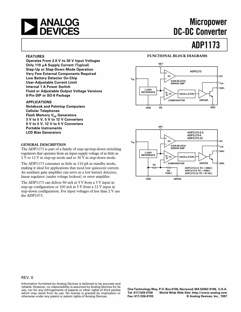
FUNCTIONAL BLOCK DIAGRAMS
SET
VINGAIN BLOCK/ERROR AMP
COMPARATOR
SW2FBGND
SW1
AO
ILIM
OSCILLATOR
DRIVER
A1
A2
1.245VREFERENCE
ADP1173
SET
VIN
GAIN BLOCK/ERROR AMP
COMPARATOR SW2
SENSEGND
SW1
AO
ILIM
OSCILLATOR
DRIVER
A1
A2
1.245VREFERENCE
ADP1173-3.3ADP1173-5ADP1173-12
R2753kΩ
R1ADP1173-3.3: R1 = 456kΩADP1173-5: R1 = 250kΩADP1173-12: R1 = 87.4kΩ
FEATURES
Operates From 2.0 V to 30 V Input Voltages
Only 110 mA Supply Current (Typical)
Step-Up or Step-Down Mode Operation
Very Few External Components Required
Low Battery Detector On-Chip
User-Adjustable Current Limit
Internal 1 A Power Switch
Fixed or Adjustable Output Voltage Versions
8-Pin DIP or SO-8 Package
APPLICATIONS
Notebook and Palmtop Computers
Cellular Telephones
Flash Memory Vpp Generators
3 V to 5 V, 5 V to 12 V Converters
9 V to 5 V, 12 V to 5 V Converters
Portable Instruments
LCD Bias Generators
GENERAL DESCRIPTIONThe ADP1173 is part of a family of step-up/step-down switchingregulators that operates from an input supply voltage of as little as2 V to 12 V in step-up mode and to 30 V in step-down mode.
The ADP1173 consumes as little as 110 µA in standby mode,making it ideal for applications that need low quiescent current.An auxiliary gain amplifier can serve as a low battery detector,linear regulator (under voltage lockout) or error amplifier.
The ADP1173 can deliver 80 mA at 5 V from a 3 V input instep-up configuration or 100 mA at 5 V from a 12 V input instep-down configuration. For input voltages of less than 2 V usethe ADP1073.
–2– REV. 0
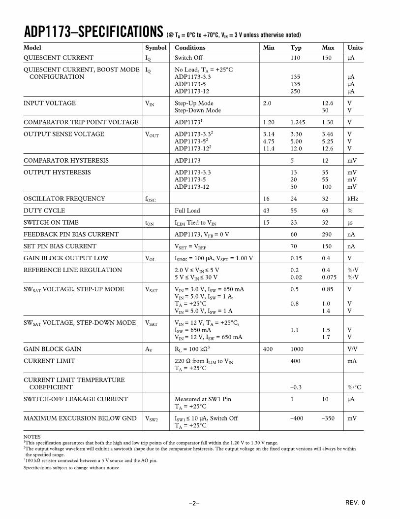
ADP1173–SPECIFICATIONS (@ TA = 08C to +708C, VIN = 3 V unless otherwise noted)
Model Symbol Conditions Min Typ Max Units
QUIESCENT CURRENT IQ Switch Off 110 150 µA
QUIESCENT CURRENT, BOOST MODE IQ No Load, TA = +25°CCONFIGURATION ADP1173-3.3 135 µA
ADP1173-5 135 µAADP1173-12 250 µA
INPUT VOLTAGE VIN Step-Up Mode 2.0 12.6 VStep-Down Mode 30 V
COMPARATOR TRIP POINT VOLTAGE ADP11731 1.20 1.245 1.30 V
OUTPUT SENSE VOLTAGE VOUT ADP1173-3.32 3.14 3.30 3.46 VADP1173-52 4.75 5.00 5.25 VADP1173-122 11.4 12.0 12.6 V
COMPARATOR HYSTERESIS ADP1173 5 12 mV
OUTPUT HYSTERESIS ADP1173-3.3 13 35 mVADP1173-5 20 55 mVADP1173-12 50 100 mV
OSCILLATOR FREQUENCY fOSC 16 24 32 kHz
DUTY CYCLE Full Load 43 55 63 %
SWITCH ON TIME tON ILIM Tied to VIN 15 23 32 µs
FEEDBACK PIN BIAS CURRENT ADP1173, VFB = 0 V 60 290 nA
SET PIN BIAS CURRENT VSET = VREF 70 150 nA
GAIN BLOCK OUTPUT LOW VOL ISINK = 100 µA, VSET = 1.00 V 0.15 0.4 V
REFERENCE LINE REGULATION 2.0 V ≤ VIN ≤ 5 V 0.2 0.4 %/V5 V ≤ VIN ≤ 30 V 0.02 0.075 %/V
SWSAT VOLTAGE, STEP-UP MODE VSAT VIN = 3.0 V, ISW = 650 mA 0.5 0.85 VVIN = 5.0 V, ISW = 1 A,TA = +25°C 0.8 1.0 VVIN = 5.0 V, ISW = 1 A 1.4 V
SWSAT VOLTAGE, STEP-DOWN MODE VSAT VIN = 12 V, TA = +25°C,ISW = 650 mA 1.1 1.5 VVIN = 12 V, ISW = 650 mA 1.7 V
GAIN BLOCK GAIN AV RL = 100 kΩ3 400 1000 V/V
CURRENT LIMIT 220 Ω from ILIM to VIN 400 mATA = +25°C
CURRENT LIMIT TEMPERATURECOEFFICIENT –0.3 %/°C
SWITCH-OFF LEAKAGE CURRENT Measured at SW1 Pin 1 10 µATA = +25°C
MAXIMUM EXCURSION BELOW GND VSW2 ISW1 ≤ 10 µA, Switch Off –400 –350 mVTA = +25°C
NOTES1This specification guarantees that both the high and low trip points of the comparator fall within the 1.20 V to 1.30 V range.2The output voltage waveform will exhibit a sawtooth shape due to the comparator hysteresis. The output voltage on the fixed output versions will always be withinthe specified range.
3100 kΩ resistor connected between a 5 V source and the AO pin.
Specifications subject to change without notice.
ADP1173
–3–REV. 0
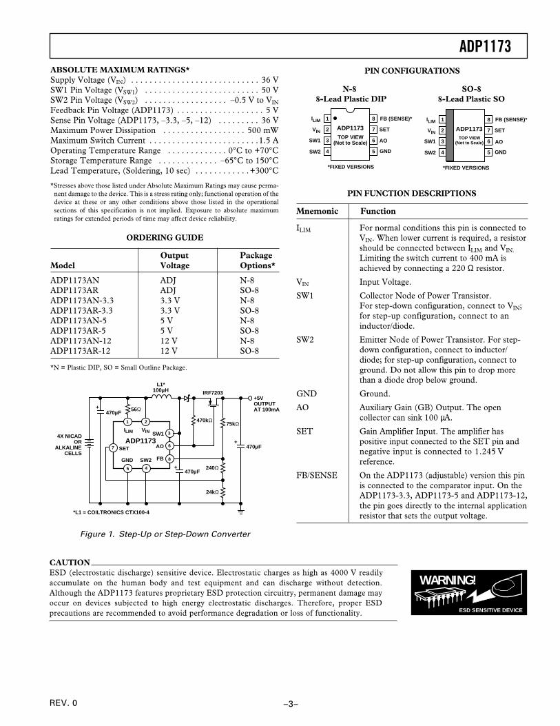
ABSOLUTE MAXIMUM RATINGS*Supply Voltage (VIN) . . . . . . . . . . . . . . . . . . . . . . . . . . . . 36 VSW1 Pin Voltage (VSW1) . . . . . . . . . . . . . . . . . . . . . . . . . 50 VSW2 Pin Voltage (VSW2) . . . . . . . . . . . . . . . . . . –0.5 V to VIN
Feedback Pin Voltage (ADP1173) . . . . . . . . . . . . . . . . . . . 5 VSense Pin Voltage (ADP1173, –3.3, –5, –12) . . . . . . . . . 36 VMaximum Power Dissipation . . . . . . . . . . . . . . . . . . 500 mWMaximum Switch Current . . . . . . . . . . . . . . . . . . . . . . . .1.5 AOperating Temperature Range . . . . . . . . . . . . . 0°C to +70°CStorage Temperature Range . . . . . . . . . . . . . –65°C to 150°CLead Temperature, (Soldering, 10 sec) . . . . . . . . . . . .+300°C
*Stresses above those listed under Absolute Maximum Ratings may cause perma-nent damage to the device. This is a stress rating only; functional operation of thedevice at these or any other conditions above those listed in the operationalsections of this specification is not implied. Exposure to absolute maximumratings for extended periods of time may affect device reliability.
ORDERING GUIDE
Output PackageModel Voltage Options*
ADP1173AN ADJ N-8ADP1173AR ADJ SO-8ADP1173AN-3.3 3.3 V N-8ADP1173AR-3.3 3.3 V SO-8ADP1173AN-5 5 V N-8ADP1173AR-5 5 V SO-8ADP1173AN-12 12 V N-8ADP1173AR-12 12 V SO-8
*N = Plastic DIP, SO = Small Outline Package.
ILIM VIN SW1ADP1173
FBSW2GND45
1 2
3
8
7 SET AO 6+
L1*100µH
470µF
75kΩ
56Ω
*L1 = COILTRONICS CTX100-4
4X NICADOR
ALKALINECELLS
240Ω
470µF+
470kΩ
24kΩ
IRF7203
+470µF
+5VOUTPUTAT 100mA
Figure 1. Step-Up or Step-Down Converter
PIN CONFIGURATIONS
N-8 SO-8 8-Lead Plastic DIP 8-Lead Plastic SO
WARNING!
ESD SENSITIVE DEVICE
CAUTIONESD (electrostatic discharge) sensitive device. Electrostatic charges as high as 4000 V readilyaccumulate on the human body and test equipment and can discharge without detection.Although the ADP1173 features proprietary ESD protection circuitry, permanent damage mayoccur on devices subjected to high energy electrostatic discharges. Therefore, proper ESDprecautions are recommended to avoid performance degradation or loss of functionality.
AO
ILIM
SW1
GND
VIN
SW2
*FIXED VERSIONS
1
2
3
4
8
7
6
5
ADP1173TOP VIEW
(Not to Scale)
FB (SENSE)*
SET
AO
ILIM
SW1
GND
VIN
SW2
*FIXED VERSIONS
1
2
3
4
8
7
6
5
ADP1173TOP VIEW
(Not to Scale)
FB (SENSE)*
SET
PIN FUNCTION DESCRIPTIONS
Mnemonic Function
ILIM For normal conditions this pin is connected toVIN. When lower current is required, a resistorshould be connected between ILIM and VIN.
Limiting the switch current to 400 mA isachieved by connecting a 220 Ω resistor.
VIN Input Voltage.
SW1 Collector Node of Power Transistor.For step-down configuration, connect to VIN;for step-up configuration, connect to aninductor/diode.
SW2 Emitter Node of Power Transistor. For step-down configuration, connect to inductor/diode; for step-up configuration, connect toground. Do not allow this pin to drop morethan a diode drop below ground.
GND Ground.
AO Auxiliary Gain (GB) Output. The opencollector can sink 100 µA.
SET Gain Amplifier Input. The amplifier haspositive input connected to the SET pin andnegative input is connected to 1.245 Vreference.
FB/SENSE On the ADP1173 (adjustable) version this pinis connected to the comparator input. On theADP1173-3.3, ADP1173-5 and ADP1173-12,the pin goes directly to the internal applicationresistor that sets the output voltage.
ADP1173
–4– REV. 0
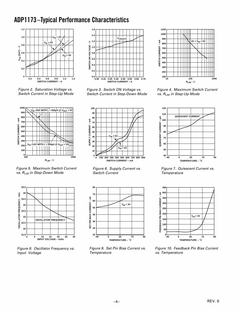
–Typical Performance Characteristics
SWITCH CURRENT – A
1.2
0.6
00.2 1.20.4 0.6 0.8 1.0
1.0
0.8
0.4
0.2
VIN = 2V
VIN = 3V
VIN = 5V
VC
E (
SA
T)
– V
Figure 2. Saturation Voltage vs. Switch Current in Step-Up Mode
RLIM – Ω
SW
ITC
H C
UR
RE
NT
– m
A
1000
900
0100 1000
800
700
600
500
400
300
200
100
VIN =24V WITH L = 500µH @ VOUT = 5V
VIN =12V WITH L = 250µH @ VOUT = 5V
Figure 5. Maximum Switch Current vs. RLIM in Step-Down Mode
INPUT VOLTAGE – Volts
OS
CIL
LA
TO
R F
RE
QU
EN
CY
– k
Hz
25.5
21.53 5 3020 25
23.5
23
22.5
22
25
24.5
24
OSCILLATOR FREQUENCY
10 15
Figure 8. Oscillator Frequency vs. Input Voltage
SWITCH CURRENT – A
SW
ITC
H O
N V
OL
TA
GE
– V
1.6
0.6
0.00.05 0.15 0.25 0.35 0.45 0.55 0.65
1.4
0.8
0.4
0.2
1.2
1.0
0.75
VCE(SAT)
Figure 3. Switch ON Voltage vs. Switch Current in Step-Down Mode
SWITCH CURRENT – mA
SU
PP
LY
CU
RR
EN
T –
mA
100
00 100 900200 300 400 600 700 800500
90
50
30
20
10
80
70
40
60
VIN = 2V
VIN = 5V
Figure 6. Supply Current vs. Switch Current
TEMPERATURE – °C
10–40 0 8525 70
50
40
30
20
80
70
60
VIN = 3V
SE
T P
IN B
IAS
CU
RR
EN
T –
nA
Figure 9. Set Pin Bias Current vs.Temperature
RLIM – Ω
SW
ITC
H C
UR
RE
NT
– m
A
1100
1000
10010 100 1000
900
800
700
600
500
400
300
200
2V < VIN < 5V
Figure 4. Maximum Switch Current vs. RLIM in Step-Up Mode
TEMPERATURE – °C
120
110
40–40 0 8525 70
80
70
60
50
100
90
QU
IES
CE
NT
CU
RR
EN
T –
µA QUIESCENT CURRENT
Figure 7. Quiescent Current vs. Temperature
TEMPERATURE – °C
0–40 0 8525 70
200
150
100
50
350
300
250
VIN = 3V
FE
ED
BA
CK
PIN
BIA
S C
UR
RE
NT
– n
A 400
450
Figure 10. Feedback Pin Bias Currentvs. Temperature
ADP1173
–5–REV. 0
APPLICATIONSTheory of OperationThe ADP1173 is a flexible, low power switch mode powersupply (SMPS) controller. The regulated output voltage can begreater than the input voltage (boost or step-up mode) or lessthan the input (buck or step-down mode). This device uses agated-oscillator technique to provide very high performancewith low quiescent current.
A functional block diagram of the ADP1173 is shown on thefront page. The internal 1.245 V reference is connected to oneinput of the comparator, while the other input is externallyconnected (via the FB pin) to a feedback network connected tothe regulated output. When the voltage at the FB pin falls below1.245 V, the 24 kHz oscillator turns on. A driver amplifier pro-vides base drive to the internal power switch, and the switchingaction raises the output voltage. When the voltage at the FB pinexceeds 1.245 V, the oscillator is shut off. While the oscillator isoff, the ADP1173 quiescent current is only 110 µA. The com-parator includes a small amount of hysteresis, which ensuresloop stability without requiring external components for fre-quency compensation.
The maximum current in the internal power switch can be setby connecting a resistor between VIN and the ILIM pin. When themaximum current is exceeded, the switch is turned OFF. Thecurrent limit circuitry has a time delay of about 2 µs. If anexternal resistor is not used, connect ILIM to VIN. Furtherinformation on ILIM is included in the Limiting the SwitchCurrent section of this data sheet.
The ADP1173 internal oscillator provides 23 µs ON and 19 µsOFF times, which is ideal for applications where the ratiobetween VIN and VOUT is roughly a factor of two (such asconverting +3 V to + 5 V). However, wider range conversions(such as generating +12 V from a +5 V supply) can easily beaccomplished.
An uncommitted gain block on the ADP1173 can be connectedas a low battery detector. The inverting input of the gain blockis internally connected to the 1.245 V reference. The noninvert-ing input is available at the SET pin. A resistor divider, con-nected between VIN and GND with the junction connected tothe SET pin, causes the AO output to go LOW when the lowbattery set point is exceeded. The AO output is an opencollector NPN transistor which can sink 100 µA.
The ADP1173 provides external connections for both thecollector and emitter of its internal power switch, which permitsboth step-up and step-down modes of operation. For the step-up mode, the emitter (pin SW2) is connected to GND and thecollector (pin SW1) drives the inductor. For step-down mode,the emitter drives the inductor while the collector is connectedto VIN.
The output voltage of the ADP1173 is set with two externalresistors. Three fixed-voltage models are also available:ADP1173-3.3 (+3.3 V), ADP1173-5 (+5 V) and ADP1173-12(+12 V). The fixed-voltage models are identical to the ADP1173,except that laser-trimmed voltage-setting resistors are includedon the chip. On the fixed-voltage models of the ADP1173,simply connect the feedback pin (Pin 8) directly to the outputvoltage.
COMPONENT SELECTIONGeneral Notes on Inductor SelectionWhen the ADP1173 internal power switch turns on, currentbegins to flow in the inductor. Energy is stored in the inductorcore while the switch is on, and this stored energy is thentransferred to the load when the switch turns off. Both thecollector and the emitter of the switch transistor are accessibleon the ADP1173, so the output voltage can be higher, lower orof opposite polarity than the input voltage.
To specify an inductor for the ADP1173, the proper values ofinductance, saturation current and dc resistance must bedetermined. This process is not difficult, and specific equationsfor each circuit configuration are provided in this data sheet. Ingeneral terms, however, the inductance value must be lowenough to store the required amount of energy (when bothinput voltage and switch ON time are at a minimum) but highenough that the inductor will not saturate when both VIN andswitch ON time are at their maximum values. The inductormust also store enough energy to supply the load withoutsaturating. Finally, the dc resistance of the inductor should below, so that excessive power will not be wasted by heating thewindings. For most ADP1173 applications, an inductor of47 µH to 470 µH, with a saturation current rating of 300 mA to1 A and dc resistance <1 Ω is suitable. Ferrite core inductorswhich meet these specifications are available in small, surface-mount packages.
To minimize Electro-Magnetic Interference (EMI), a toroid orpot core type inductor is recommended. Rod core inductors area lower cost alternative if EMI is not a problem.
CALCULATING THE INDUCTOR VALUESelecting the proper inductor value is a simple three-stepprocess:
1. Define the operating parameters: minimum input voltage,maximum input voltage, output voltage and output current.
2. Select the appropriate conversion topology (step-up, step-down, or inverting).
3. Calculate the inductor value, using the equations in thefollowing sections.
Inductor Selection—Step-Up ConverterIn a step-up, or boost, converter (Figure 14), the inductor muststore enough power to make up the difference between theinput voltage and the output voltage. The power that must bestored is calculated from the equation:
PL = VOUT +V D –V IN(MIN)( )× IOUT( ) (1)
where VD is the diode forward voltage (≈ 0.5 V for a 1N5818Schottky). Energy is only stored in the inductor while theADP1173 switch is ON, so the energy stored in the inductor oneach switching cycle must be must be equal to or greater than:
PL
fOSC(2)
in order for the ADP1173 to regulate the output voltage.
ADP1173
–6– REV. 0
When the internal power switch turns ON, current flow in theinductor increases at the rate of:
IL (t)=
V IN
R′1– e
–R′tL
(3)
where L is in henrys and R' is the sum of the switch equivalentresistance (typically 0.8 Ω at +25°C) and the dc resistance ofthe inductor. In most applications, where the voltage drop acrossthe switch is small compared to VIN , a simpler equation can beused:
IL (t)=
V IN
Lt (4)
Replacing “t” in the above equation with the ON time of theADP1173 (23 µs, typical) will define the peak current for agiven inductor value and input voltage. At this point, theinductor energy can be calculated as follows:
EL =
12
LI 2PEAK (5)
As previously mentioned, EL must be greater than PL/fOSC so theADP1173 can deliver the necessary power to the load. For bestefficiency, peak current should be limited to 1 A or less. Higherswitch currents will reduce efficiency, because of increasedsaturation voltage in the switch. High peak current also increasesoutput ripple. As a general rule, keep peak current as low as pos-sible to minimize losses in the switch, inductor and diode.
In practice, the inductor value is easily selected using the equa-tions above. For example, consider a supply that will generate9 V at 50 mA from a 3 V source. The inductor power requiredis, from Equation 1:
PL = (9V +0.5V –3V )×(50 mA)= 325 mW
On each switching cycle, the inductor must supply:
PL
fOSC=
325 mW24 kHz
=13.5µJ
The required inductor power is fairly low in this example, so thepeak current can also be low. Assuming a peak current of 500 mAas a starting point, Equation 4 can be rearranged to recommendan inductor value:
L =
V IN
IL(MAX )t =
3V500 mA
23 µs =138 µH
Substituting a standard inductor value of 100 µH, with 0.2 Ω dcresistance, will produce a peak switch current of:
IPEAK =3V
1.0 Ω1– e
–1.0 Ω × 23 µs100 µH
= 616 mA
Once the peak current is known, the inductor energy can becalculated from Equation 5:
EL =
12
(100 µH )×(616 mA)2 =19 µJ
The inductor energy of 19 µJ is greater than the PL/fOSC re-quirement of 13.5 µJ, so the 100 µH inductor will work in thisapplication. By substituting other inductor values into the sameequations, the optimum inductor value can be selected.
When selecting an inductor, the peak current must not exceedthe maximum switch current of 1.5 A. If the equations shownabove result in peak currents > 1.5 A, the ADP1073 should beconsidered. This device has a 72% duty cycle, so more energy isstored in the inductor on each cycle. This results in greateroutput power.
The peak current must be evaluated for both minimum andmaximum values of input voltage. If the switch current is highwhen VIN is at its minimum, then the 1.5 A limit may be ex-ceeded at the maximum value of VIN. In this case, the ADP1173’scurrent limit feature can be used to limit switch current. Simplyselect a resistor (using Figure 4) that will limit the maximumswitch current to the IPEAK value calculated for the minimumvalue of VIN. This will improve efficiency by producing a con-stant IPEAK as VIN increases. See the Limiting the Switch Currentsection of this data sheet for more information.
Note that the switch current limit feature does not protect thecircuit if the output is shorted to ground. In this case, current isonly limited by the dc resistance of the inductor and the forwardvoltage of the diode.
Inductor Selection—Step-Down ConverterThe step-down mode of operation is shown in Figure 15. Unlikethe step-up mode, the ADP1173’s power switch does notsaturate when operating in the step-down mode. Therefore,switch current should be limited to 650 mA in this mode. If theinput voltage will vary over a wide range, the ILIM pin can beused to limit the maximum switch current. If higher outputcurrent is required, the ADP1111 should be considered.
The first step in selecting the step-down inductor is to calculatethe peak switch current as follows:
IPEAK =
2IOUT
DCVOUT +V D
V IN –VSW +V D
(6)
where DC = duty cycle (0.55 for the ADP1173)
VSW = voltage drop across the switchVD = diode drop (0.5 V for a 1N5818)IOUT = output currentVOUT = the output voltageVIN = the minimum input voltage
As previously mentioned, the switch voltage is higher in step-down mode than step-up mode. VSW is a function of switchcurrent and is therefore a function of VIN, L, time and VOUT.For most applications, a VSW value of 1.5 V is recommended.
The inductor value can now be calculated:
L =
V IN(MIN) –VSW –VOUT
IPEAK× tON (7)
where tON = switch ON time (23 µs)
If the input voltage will vary (such as an application that mustoperate from a 12 V to 24 V source) an RLIM resistor should beselected from Figure 5. The RLIM resistor will keep switch cur-rent constant as the input voltage rises. Note that there are separateRLIM values for step-up and step-down modes of operation.
ADP1173
–7–REV. 0
For example, assume that +5 V at 300 mA is required from a12 V to +24 V input. Deriving the peak current from Equation 6yields:
IPEAK =
2×300 mA0.55
5 + 0.512 –1.5 + 0.5
= 545 mA
The peak current can then be inserted into Equation 7 to calcu-late the inductor value:
L =
12 –1.5–5545 mA
×23 µs = 232 µH
Since 232 µH is not a standard value, the next lower standardvalue of 220 µH would be specified.
To avoid exceeding the maximum switch current when theinput voltage is at +24 V, an RLIM resistor should be specified.Using the step-down curve of Figure 5, a value of 180 Ω willlimit the switch current to 600 mA.
Inductor Selection—Positive-to-Negative ConverterThe configuration for a positive-to-negative converter using theADP1173 is shown in Figure 17. As with the step-up converter,all of the output power for the inverting circuit must be suppliedby the inductor. The required inductor power is derived fromthe formula:
PL = |VOUT|+V D( )× IOUT( ) (8)
The ADP1173 power switch does not saturate in positive-to-negative mode. The voltage drop across the switch can bemodeled as a 0.75 V base-emitter diode in series with a 0.65 Ωresistor. When the switch turns on, inductor current will rise ata rate determined by:
IL (t)=
V L
R'1– e
_R'tL
(9)
where R' = 0.65 Ω + RL(DC)
where VL = VIN – 0.75 V
For example, assume that a –5 V output at 50 mA is to begenerated from a +4.5 V to +5.5 V source. The power in theinductor is calculated from Equation 8:
PL = |−5V|+ 0.5V( )×(50 mA)= 275 mW
During each switching cycle, the inductor must supply thefollowing energy:
PL
fOSC=
275 mW24 kHz
=11.5µJ
Using a standard inductor value of 220 µH, with 0.2 Ω dcresistance, will produce a peak switch current of:
IPEAK =4.5V –0.75V0.65 Ω +0.2 Ω
1– e–0.85Ω × 23 µs
220 µH
= 375 mA
Once the peak current is known, the inductor energy can becalculated from Equation 5:
EL =
12
(220 µH )×(375 mA)2 =15.5µJ
The inductor energy of 15.5 µJ is greater than the PL/fOSC
requirement of 11.5 µJ, so the 220 µH inductor will work inthis application.
The input voltage only varies between 4.5 V and 5.5 V in thisexample. Therefore, the peak current will not change enough torequire an RLIM resistor and the ILIM pin can be connecteddirectly to VIN. Care should be taken to ensure that the peakcurrent does not exceed 650 mA.
CAPACITOR SELECTIONFor optimum performance, the ADP1173’s output capacitormust be carefully selected. Choosing an inappropriate capacitorcan result in low efficiency and/or high output ripple.
Ordinary aluminum electrolytic capacitors are inexpensive, butoften have poor Equivalent Series Resistance (ESR) andEquivalent Series Inductance (ESL). Low ESR aluminum ca-pacitors, specifically designed for switch mode converter appli-cations, are also available, and these are a better choice thangeneral purpose devices. Even better performance can beachieved with tantalum capacitors, although their cost is higher.Very low values of ESR can be achieved by using OS-CON*capacitors (Sanyo Corporation, San Diego, CA). These devicesare fairly small, available with tape-and-reel packaging, and havevery low ESR.
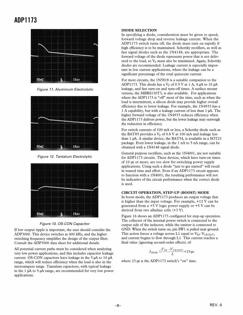
The effects of capacitor selection on output ripple are demon-strated in Figures 11, 12, and 13. These figures show the outputof the same ADP1173 converter, which was evaluated withthree different output capacitors. In each case, the peak switchcurrent is 500 mA and the capacitor value is 100 µF. Figure 11shows a Panasonic HF-series* radial aluminum electrolytic.When the switch turns off, the output voltage jumps by about90 mV and then decays as the inductor discharges into thecapacitor. The rise in voltage indicates an ESR of about0.18 Ω. In Figure 12, the aluminum electrolytic has beenreplaced by a Sprague 593D-series* tantalum device. In thiscase the output jumps about 35 mV, which indicates an ESR of0.07 Ω. Figure 13 shows an OS-CON SA series capacitor in thesame circuit, and ESR is only 0.02 Ω.
*All trademarks are properties of their respective holders.
ADP1173
–8– REV. 0
Figure 11. Aluminum Electrolytic
Figure 12. Tantalum Electrolytic
Figure 13. OS-CON Capacitor
If low output ripple is important, the user should consider theADP3000. This device switches at 400 kHz, and the higherswitching frequency simplifies the design of the output filter.Consult the ADP3000 data sheet for additional details.
All potential current paths must be considered when analyzingvery low power applications, and this includes capacitor leakagecurrent. OS-CON capacitors have leakage in the 5 µA to 10 µArange, which will reduce efficiency when the load is also in themicroampere range. Tantalum capacitors, with typical leakagein the 1 µA to 5 µA range, are recommended for very low powerapplications.
DIODE SELECTIONIn specifying a diode, consideration must be given to speed,forward voltage drop and reverse leakage current. When theADP1173 switch turns off, the diode must turn on rapidly ifhigh efficiency is to be maintained. Schottky rectifiers, as well asfast signal diodes such as the 1N4148, are appropriate. Theforward voltage of the diode represents power that is not deliv-ered to the load, so VF must also be minimized. Again, Schottkydiodes are recommended. Leakage current is especially impor-tant in low current applications, where the leakage can be asignificant percentage of the total quiescent current.
For most circuits, the 1N5818 is a suitable companion to theADP1173. This diode has a VF of 0.5 V at 1 A, 4 µA to 10 µAleakage, and fast turn-on and turn-off times. A surface mountversion, the MBRS130T3, is also available. For applicationswhere the ADP1173 is “off” most of the time, such as when theload is intermittent, a silicon diode may provide higher overallefficiency due to lower leakage. For example, the 1N4933 has a1 A capability, but with a leakage current of less than 1 µA. Thehigher forward voltage of the 1N4933 reduces efficiency whenthe ADP1173 delivers power, but the lower leakage may outweighthe reduction in efficiency.
For switch currents of 100 mA or less, a Schottky diode such asthe BAT85 provides a VF of 0.8 V at 100 mA and leakage lessthan 1 µA. A similar device, the BAT54, is available in a SOT23package. Even lower leakage, in the 1 nA to 5 nA range, can beobtained with a 1N4148 signal diode.
General purpose rectifiers, such as the 1N4001, are not suitablefor ADP1173 circuits. These devices, which have turn-on timesof 10 µs or more, are too slow for switching power supplyapplications. Using such a diode “just to get started” will resultin wasted time and effort. Even if an ADP1173 circuit appearsto function with a 1N4001, the resulting performance will notbe indicative of the circuit performance when the correct diodeis used.
CIRCUIT OPERATION, STEP-UP (BOOST) MODEIn boost mode, the ADP1173 produces an output voltage thatis higher than the input voltage. For example, +12 V can begenerated from a +5 V logic power supply or +5 V can bederived from two alkaline cells (+3 V).
Figure 16 shows an ADP1173 configured for step-up operation.The collector of the internal power switch is connected to theoutput side of the inductor, while the emitter is connected toGND. When the switch turns on, pin SW1 is pulled near ground.This action forces a voltage across L1 equal to VIN–VCE(SAT),
and current begins to flow through L1. This current reaches afinal value (ignoring second-order effects) of:
IPEAK ≅
V IN –VCE(SAT )
L×23 µs
where 23 µs is the ADP1173 switch’s “on” time.
ADP1173
–9–REV. 0
+ILIM VIN SW1
ADP1173
VIN
L1 D1
C1
R2
R1
VOUT
R3*
FB
* = OPTIONAL
SW2GND
45
1 2
3
8
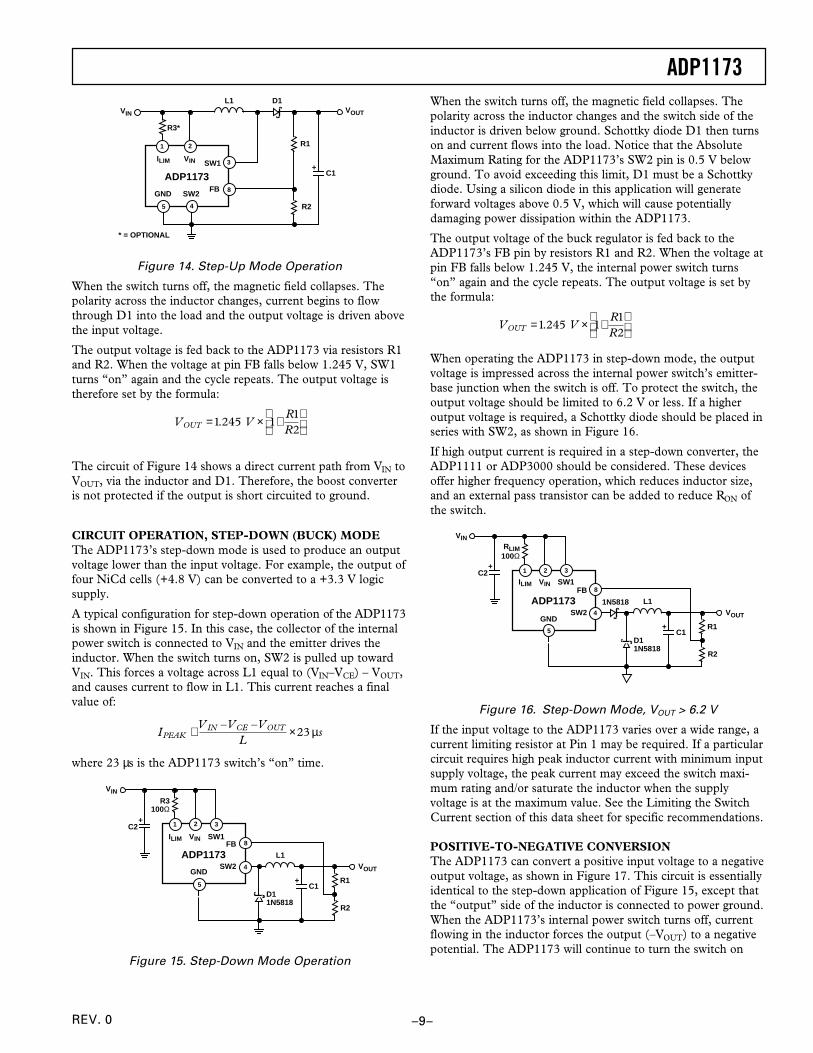
Figure 14. Step-Up Mode Operation
When the switch turns off, the magnetic field collapses. Thepolarity across the inductor changes, current begins to flowthrough D1 into the load and the output voltage is driven abovethe input voltage.
The output voltage is fed back to the ADP1173 via resistors R1and R2. When the voltage at pin FB falls below 1.245 V, SW1turns “on” again and the cycle repeats. The output voltage istherefore set by the formula:
VOUT =1.245 V × 1+
R1R2
The circuit of Figure 14 shows a direct current path from VIN toVOUT, via the inductor and D1. Therefore, the boost converteris not protected if the output is short circuited to ground.
CIRCUIT OPERATION, STEP-DOWN (BUCK) MODEThe ADP1173’s step-down mode is used to produce an outputvoltage lower than the input voltage. For example, the output offour NiCd cells (+4.8 V) can be converted to a +3.3 V logicsupply.
A typical configuration for step-down operation of the ADP1173is shown in Figure 15. In this case, the collector of the internalpower switch is connected to VIN and the emitter drives theinductor. When the switch turns on, SW2 is pulled up towardVIN. This forces a voltage across L1 equal to (VIN–VCE) – VOUT,and causes current to flow in L1. This current reaches a finalvalue of:
IPEAK ≅
V IN –VCE –VOUT
L×23 µs
where 23 µs is the ADP1173 switch’s “on” time.
ILIM VINFB
ADP1173SW2
GND
5
1 2
8SW1
3
R3100Ω
+C2
VIN
L1
D11N5818
+C1
VOUT
R2
R1
4
Figure 15. Step-Down Mode Operation
When the switch turns off, the magnetic field collapses. Thepolarity across the inductor changes and the switch side of theinductor is driven below ground. Schottky diode D1 then turnson and current flows into the load. Notice that the AbsoluteMaximum Rating for the ADP1173’s SW2 pin is 0.5 V belowground. To avoid exceeding this limit, D1 must be a Schottkydiode. Using a silicon diode in this application will generateforward voltages above 0.5 V, which will cause potentiallydamaging power dissipation within the ADP1173.
The output voltage of the buck regulator is fed back to theADP1173’s FB pin by resistors R1 and R2. When the voltage atpin FB falls below 1.245 V, the internal power switch turns“on” again and the cycle repeats. The output voltage is set bythe formula:
VOUT =1.245 V × 1+
R1R2
When operating the ADP1173 in step-down mode, the outputvoltage is impressed across the internal power switch’s emitter-base junction when the switch is off. To protect the switch, theoutput voltage should be limited to 6.2 V or less. If a higheroutput voltage is required, a Schottky diode should be placed inseries with SW2, as shown in Figure 16.
If high output current is required in a step-down converter, theADP1111 or ADP3000 should be considered. These devicesoffer higher frequency operation, which reduces inductor size,and an external pass transistor can be added to reduce RON ofthe switch.
ILIM VINFB
ADP1173SW2
GND
5
1 2
8SW1
3
RLIM100Ω
+C2
L1
D11N5818
+C1
VOUT
R2
R1
1N5818
VIN
4
Figure 16. Step-Down Mode, VOUT > 6.2 V
If the input voltage to the ADP1173 varies over a wide range, acurrent limiting resistor at Pin 1 may be required. If a particularcircuit requires high peak inductor current with minimum inputsupply voltage, the peak current may exceed the switch maxi-mum rating and/or saturate the inductor when the supplyvoltage is at the maximum value. See the Limiting the SwitchCurrent section of this data sheet for specific recommendations.
POSITIVE-TO-NEGATIVE CONVERSIONThe ADP1173 can convert a positive input voltage to a negativeoutput voltage, as shown in Figure 17. This circuit is essentiallyidentical to the step-down application of Figure 15, except thatthe “output” side of the inductor is connected to power ground.When the ADP1173’s internal power switch turns off, currentflowing in the inductor forces the output (–VOUT) to a negativepotential. The ADP1173 will continue to turn the switch on
ADP1173
–10– REV. 0
until its FB pin is 1.245 V above its GND pin, so the outputvoltage is determined by the formula:
–VOUT =1.245 V × 1+
R1R2
ILIM VINFB
ADP1173SW2
GND5
1 2
8SW1
3
R3
+C2
+VIN
L1
D11N5818
+C1
–VOUT
R2
R1
4
Figure 17. A Positive-to-Negative Converter
The design criteria for the step-down application also apply tothe positive-to-negative converter. The output voltage should belimited to |6.2 V|, unless a diode is inserted in series with theSW2 Pin (see Figure 16). Also, D1 must again be a Schottkydiode to prevent excessive power dissipation in the ADP1173.
NEGATIVE-TO-POSITIVE CONVERSIONThe circuit of Figure 18 converts a negative input voltage to apositive output voltage. Operation of this circuit configuration issimilar to the step-up topology of Figure 14, except that the currentthrough feedback resistor R1 is level-shifted below ground by aPNP transistor. The voltage across R1 is (VOUT–VBEQ1). How-ever, diode D2 level-shifts the base of Q1 about 0.6 V belowground, thereby cancelling the VBE of Q1. The addition of D2also reduces the circuit’s output voltage sensitivity to tempera-ture, which otherwise would be dominated by the –2 mV/°C VBE
contribution of Q1. The output voltage for this circuit is deter-mined by the formula:
VOUT = 1.245 V × R1
R2
Unlike the positive step-up converter, the negative-to-positiveconverter’s output voltage can be either higher or lower than theinput voltage.
+
ILIM VINSW1
ADP1173
L1
CLRLIM
FB
SW2GND45
1 2
3
8
SET7
AO6
+C2
NEGATIVEINPUT
NC NC
R1
1N5818D1
R2
10kΩ
Q12N3906
1N4148D2
POSITIVEOUTPUT
Figure 18. A Negative-to-Positive Converter
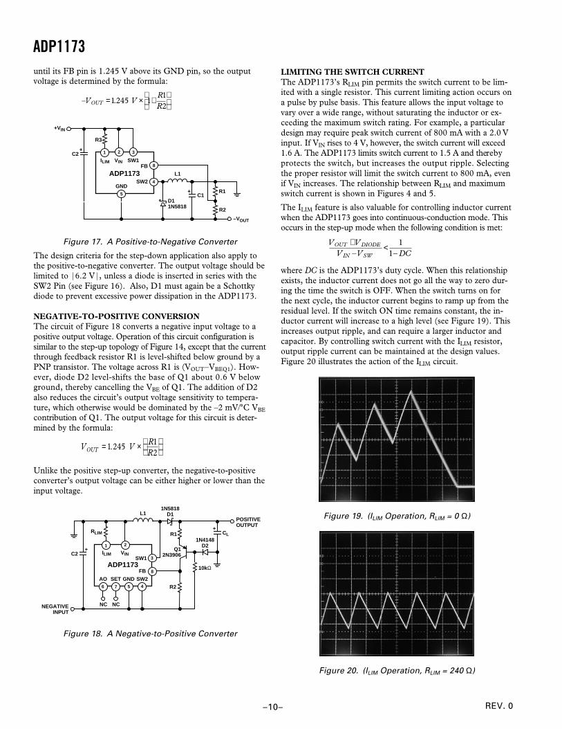
LIMITING THE SWITCH CURRENTThe ADP1173’s RLIM pin permits the switch current to be lim-ited with a single resistor. This current limiting action occurs ona pulse by pulse basis. This feature allows the input voltage tovary over a wide range, without saturating the inductor or ex-ceeding the maximum switch rating. For example, a particulardesign may require peak switch current of 800 mA with a 2.0 Vinput. If VIN rises to 4 V, however, the switch current will exceed1.6 A. The ADP1173 limits switch current to 1.5 A and therebyprotects the switch, but increases the output ripple. Selectingthe proper resistor will limit the switch current to 800 mA, evenif VIN increases. The relationship between RLIM and maximumswitch current is shown in Figures 4 and 5.
The ILIM feature is also valuable for controlling inductor currentwhen the ADP1173 goes into continuous-conduction mode. Thisoccurs in the step-up mode when the following condition is met:
VOUT +V DIODE
V IN –VSW<
11– DC
where DC is the ADP1173’s duty cycle. When this relationshipexists, the inductor current does not go all the way to zero dur-ing the time the switch is OFF. When the switch turns on forthe next cycle, the inductor current begins to ramp up from theresidual level. If the switch ON time remains constant, the in-ductor current will increase to a high level (see Figure 19). Thisincreases output ripple, and can require a larger inductor andcapacitor. By controlling switch current with the ILIM resistor,output ripple current can be maintained at the design values.Figure 20 illustrates the action of the ILIM circuit.
Figure 19. (ILIM Operation, RLIM = 0 Ω)
Figure 20. (ILIM Operation, RLIM = 240 Ω)
ADP1173
–11–REV. 0
The internal structure of the ILIM circuit is shown in Figure 21.Q1 is the ADP1173’s internal power switch, which is paralleledby sense transistor Q2. The relative sizes of Q1 and Q2 arescaled so that IQ2 is 0.5% of IQ1. Current flows to Q2 through aninternal 80 Ω resistor and through the RLIM resistor. These tworesistors parallel the base-emitter junction of the oscillator-disable transistor, Q3. When the voltage across R1 and RLIM
exceeds 0.6 V, Q3 turns on and terminates the output pulse. Ifonly the 80 Ω internal resistor is used (i.e., the ILIM pin is con-nected directly to VIN), the maximum switch current will be1.5 A. Figures 4 and 5 gives RLIM values for lower current-limitvalues.
OSCILLATOR
VIN
SW2
SW1
RLIM
DRIVER
80Ω(INTERNAL)
ILIM
(EXTERNAL)
Q2 Q1
Q3
R1
Figure 21. Current Limit Operation
The delay through the current limiting circuit is approximately2 µs. If the switch ON time is reduced to less than 4 µs, accu-racy of the current trip-point is reduced. Attempting to programa switch ON time of 2 µs or less will produce spurious responsesin the switch ON time. However, the ADP1173 will still providea properly regulated output voltage.
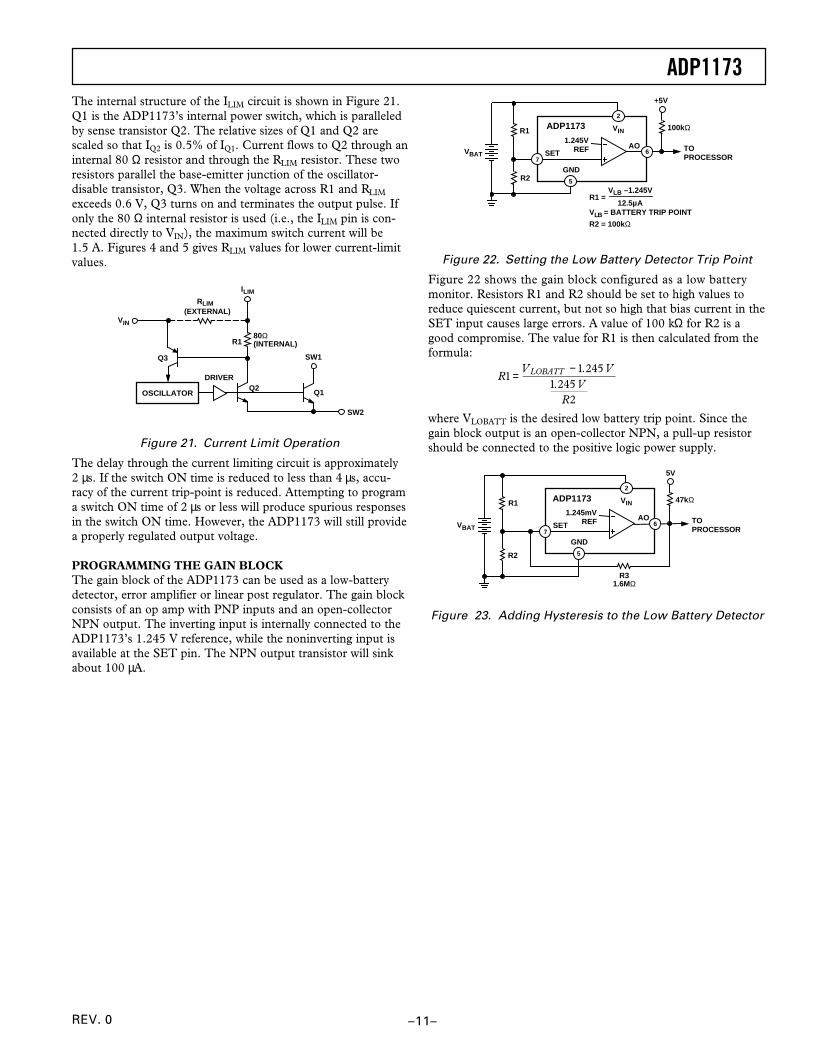
PROGRAMMING THE GAIN BLOCKThe gain block of the ADP1173 can be used as a low-batterydetector, error amplifier or linear post regulator. The gain blockconsists of an op amp with PNP inputs and an open-collectorNPN output. The inverting input is internally connected to theADP1173’s 1.245 V reference, while the noninverting input isavailable at the SET pin. The NPN output transistor will sinkabout 100 µA.
2
VIN
+5V
GND
ADP1173R1
AOSET
5R2
100kΩ
TOPROCESSOR
6
1.245VREF
7VBAT
VLB –1.245V
12.5µAVLB = BATTERY TRIP POINT
R2 = 100kΩ
R1 =
Figure 22. Setting the Low Battery Detector Trip Point
Figure 22 shows the gain block configured as a low batterymonitor. Resistors R1 and R2 should be set to high values toreduce quiescent current, but not so high that bias current in theSET input causes large errors. A value of 100 kΩ for R2 is agood compromise. The value for R1 is then calculated from theformula:
R1 =V LOBATT − 1.245 V
1.245 VR2
where VLOBATT is the desired low battery trip point. Since thegain block output is an open-collector NPN, a pull-up resistorshould be connected to the positive logic power supply.
2
VIN
5V
GND
ADP1173R1
AOSET
5R2
47kΩ
TOPROCESSOR
6
1.245mVREF
7VBAT
R31.6MΩ
Figure 23. Adding Hysteresis to the Low Battery Detector
ADP1173
–12– REV. 0
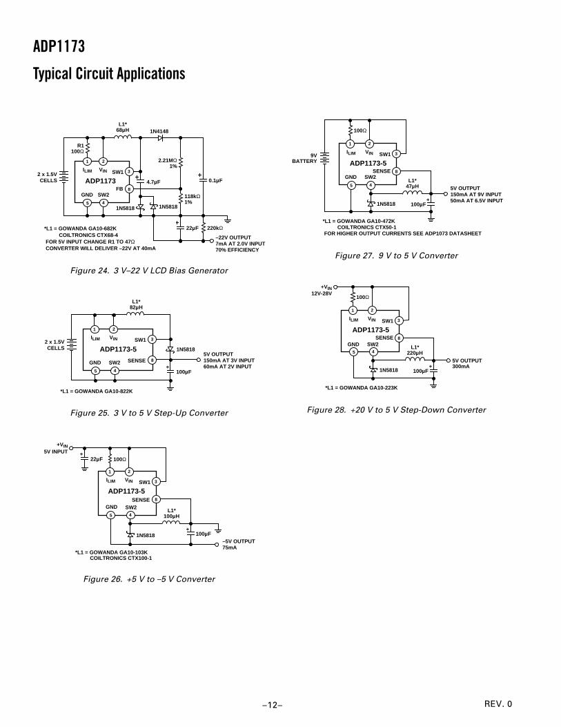
Typical Circuit Applications
ILIM VIN SW1
ADP1173
L1*68µH 1N4148
0.1µF
118kΩ1%
2.21MΩ1%
R1100Ω
FBSW2GND
45
1 2
3
8
2 x 1.5VCELLS 4.7µF
1N5818 1N5818
220kΩ22µF*L1 = GOWANDA GA10-682K COILTRONICS CTX68-4 FOR 5V INPUT CHANGE R1 TO 47Ω CONVERTER WILL DELIVER –22V AT 40mA
–22V OUTPUT7mA AT 2.0V INPUT70% EFFICIENCY
Figure 24. 3 V–22 V LCD Bias Generator
ILIM VIN SW1
ADP1173-5
L1*82µH
SENSESW2GND45
1 2
3
8
2 x 1.5VCELLS 1N5818
100µF+
5V OUTPUT150mA AT 3V INPUT60mA AT 2V INPUT
*L1 = GOWANDA GA10-822K
Figure 25. 3 V to 5 V Step-Up Converter
ILIM VIN SW1
ADP1173-5
L1*100µH
100Ω
SENSESW2GND
45
1 2
3
8
*L1 = GOWANDA GA10-103K COILTRONICS CTX100-1
–5V OUTPUT75mA
+22µF
+VIN5V INPUT
1N5818+
100µF
Figure 26. +5 V to –5 V Converter
ILIM VIN SW1
ADP1173-5
L1*47µH
100Ω
SENSESW2GND
45
1 2
3
8
*L1 = GOWANDA GA10-472K COILTRONICS CTX50-1 FOR HIGHER OUTPUT CURRENTS SEE ADP1073 DATASHEET
5V OUTPUT150mA AT 9V INPUT50mA AT 6.5V INPUT
1N5818+
100µF
9VBATTERY
Figure 27. 9 V to 5 V Converter
ILIM VIN SW1
ADP1173-5
L1*220µH
100Ω
SENSESW2GND
45
1 2
3
8
*L1 = GOWANDA GA10-223K
5V OUTPUT300mA
1N5818+
100µF
+VIN12V-28V
Figure 28. +20 V to 5 V Step-Down Converter
ADP1173
–13–REV. 0
L1*500µH MUR110
110kΩ
+
100Ω
220µF10V
3.6MΩ
1N4148
IRF530
390kΩ
2N5400
+5V100mA
10kΩ
1N965B
10nF
+ 47µF100V
VN2222L
~
+
–
~44mH
44mH
48V DC
*L1 = CTX110077 IQ = 120µA
12V
+ 10µF16V
15V
ILIM VIN SW1
ADP1173FBSW2GND
45
1 2
3
8
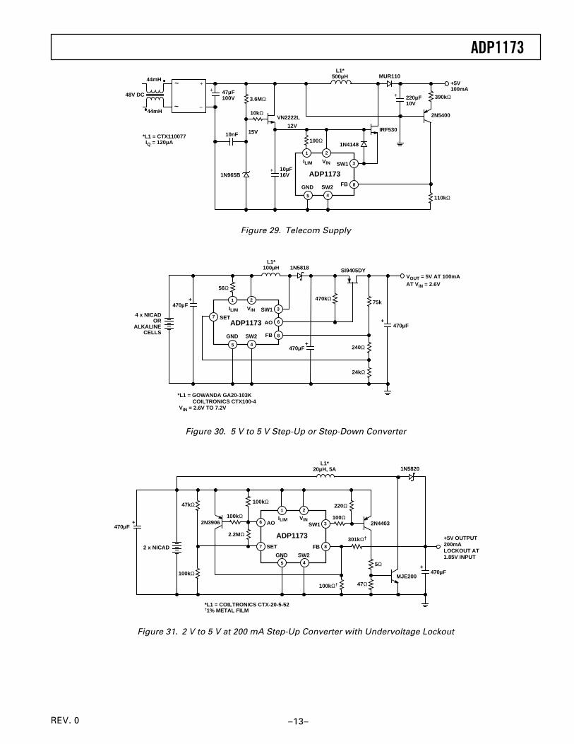
Figure 29. Telecom Supply
ILIM VIN SW1
ADP1173
FBSW2GND45
1 2
3
8
7 SETAO 6 +
L1*100µH 1N5818
470µF
75k
+
56Ω
*L1 = GOWANDA GA20-103K COILTRONICS CTX100-4 VIN = 2.6V TO 7.2V
4 x NICADOR
ALKALINECELLS
240Ω470µF
470µF+ 470kΩ
24kΩ
SI9405DY VOUT = 5V AT 100mA AT VIN = 2.6V
Figure 30. 5 V to 5 V Step-Up or Step-Down Converter
+
L1*20µH, 5A
470µF
*L1 = COILTRONICS CTX-20-5-52†1% METAL FILM
2 x NICAD
5Ω
47Ω
47kΩ
100kΩ
100kΩ
2.2MΩ
100kΩ2N3906
220Ω
100kن
301kن
2N4403
MJE200
1N5820
+5V OUTPUT200mALOCKOUT AT1.85V INPUT
100ΩILIM VINSW1
ADP1173FB
SW2GND5
1 2
3
87 SET
AO6470µF
+
4
Figure 31. 2 V to 5 V at 200 mA Step-Up Converter with Undervoltage Lockout
ADP1173
–14– REV. 0
+
L1*25µH, 2A
2N3904 470µF
*L1 = GOWANDA GT10-100 EFFICIENCY ≥ 80% FOR 10mA ≤ ILOAD ≤ 500mA STANDBY IQ ≤ 150µA
2kΩ
MTM20P08
18V1W
100Ω1/2W
51Ω
0.22ΩVIN
7V-24V
1N4148
1N58201N5818
VIN 39kΩ200kΩ
OP196VC (0V TO +5V)
–VOUT = –5.13*VC
ILIM VIN SW1
ADP1173
FBSW2GND45
1 2
3
8
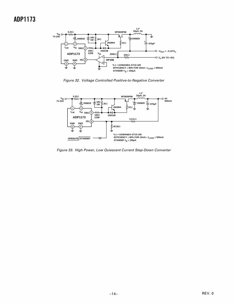
Figure 32. Voltage Controlled Positive-to-Negative Converter
40.2kΩ
+
L1*25µH, 2A
2N3904470µF
*L1 = GOWANDA GT10-100 EFFICIENCY ≥ 80% FOR 10mA ≤ ILOAD ≤ 500mA STANDBY IQ ≤ 150µA
2kΩ
MTM20P08
OPERATE STANDBY
18V1W
100Ω1/2W
51Ω
0.22ΩVIN
7V-24V
1N4148
1N58201N5818
121kΩ
ILIM VIN SW1
ADP1173FB
SW2GND45
1 2
3
8
5V500mA
Figure 33. High Power, Low Quiescent Current Step-Down Converter
ADP1173
–15–REV. 0
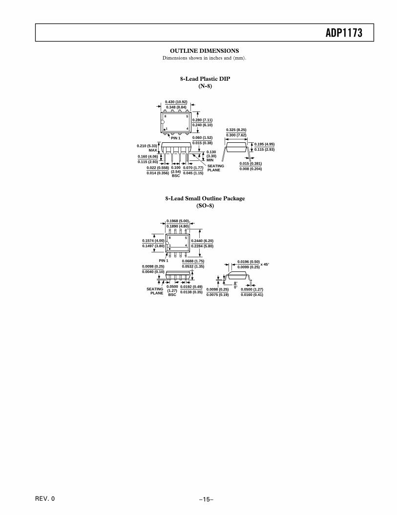
OUTLINE DIMENSIONSDimensions shown in inches and (mm).
8-Lead Plastic DIP(N-8)
8
1 4
5
0.430 (10.92)0.348 (8.84)
0.280 (7.11)0.240 (6.10)
PIN 1
SEATINGPLANE
0.022 (0.558)0.014 (0.356)
0.060 (1.52)0.015 (0.38)
0.210 (5.33)MAX 0.130
(3.30)MIN
0.070 (1.77)0.045 (1.15)
0.100(2.54)BSC
0.160 (4.06)0.115 (2.93)
0.325 (8.25)0.300 (7.62)
0.015 (0.381)0.008 (0.204)
0.195 (4.95)0.115 (2.93)
8-Lead Small Outline Package(SO-8)
0.1968 (5.00)0.1890 (4.80)
8 5
410.2440 (6.20)0.2284 (5.80)
PIN 1
0.1574 (4.00)0.1497 (3.80)
0.0688 (1.75)0.0532 (1.35)
SEATINGPLANE
0.0098 (0.25)0.0040 (0.10)
0.0192 (0.49)0.0138 (0.35)
0.0500(1.27)BSC
0.0098 (0.25)0.0075 (0.19)
0.0500 (1.27)0.0160 (0.41)
8°0°
0.0196 (0.50)0.0099 (0.25)
x 45°

–16–
C29
65–1
2–1/
97P
RIN
TE
D IN
U.S
.A.