a coplanar waveguide uwb antenna with notch filter
TRANSCRIPT
A Coplanar Waveguide UWB Antenna With Notch Filter
by
Qianqian Wang
B.Eng., University of Victoria, 2012
A Thesis Submitted in Partial Fulfillment of the
Requirements for the Degree of
MASTER OF APPLIED SCIENCE
in the Department of Electrical and Computer Engineering
University of Victoria, British Columbia
c© Qianqian Wang, 2012
University of Victoria
All rights reserved. This dissertation may not be reproduced in whole or in part, by
photocopying or other means, without the permission of the author.
ii
A Coplanar Waveguide UWB Antenna With Notch Filter
by
Qianqian Wang
B.Eng., University of Victoria, 2012
Supervisory Committee
Dr. Jens Bornemann, Supervisor
(Department of Electrical and Computer Engineering)
Dr. Poman So, Departmental Member
(Department of Electrical and Computer Engineering)
Dr. Member Two, Departmental Member
(Department of Same As Candidate)
iii
ABSTRACT
Due to the release of 3.1-10.6 GHz band, UWB systems have a rapidly progressive
development. They have been widely employed in short-range communication ap-
plications and large-bandwidth handheld devices. As part of the system, the UWB
antenna plays an extremely important role. Due to the trend towards integrated
printed circuits, co-planar waveguide technology is a feasible solution for designing
the UWB antenna.
This thesis focuses on designing a UWB co-planar waveguide antenna with a band-
stop filter. This band-stop filter offers rejection to unwanted frequencies in the range
of the operating band in order to avoid unnecessary interference from other commu-
nication applications and improve its own systems performance. In addition, it can
divide the whole wide band into a few sub-bands. This will create more flexibility for
practical applications.
The professional full-wave field solver software package CST Microwave Studio
is used as the analysis tool to obtain the performances of this antenna. It operates
from 3.1 GHz to 10.6 GHz with a VSWR < 2 in the pass bands, and a VSWR >
2 in the stop bands. The selected frequencies demonstrate nearly omni-directional
characteristics in radiation patterns. Comparing with other published UWB antenna
designs, relatively reasonable group delay results are achieved. Measurements on a
fabricated prototype validate the design approach.
iv
Contents
Supervisory Committee ii
Abstract iii
Table of Contents iv
List of Tables vii
List of Figures viii
List of Acronyms xiv
Acknowledgements xvi
1 Introduction 1
1.1 Purpose of Thesis . . . . . . . . . . . . . . . . . . . . . . . . . . . . . 2
1.2 Contributions . . . . . . . . . . . . . . . . . . . . . . . . . . . . . . . 3
1.3 Thesis Overview . . . . . . . . . . . . . . . . . . . . . . . . . . . . . . 4
2 Fundamentals of Ultra Wideband Technology 6
2.1 Development of Ultra Wideband Technology and Antennas . . . . . . 9
2.1.1 History of Ultra Wideband Technology . . . . . . . . . . . . . 9
2.1.2 Development of Ultra Wideband Antenna . . . . . . . . . . . 10
v
2.2 Ultra Wideband Antenna Design Principle . . . . . . . . . . . . . . . 16
2.2.1 Antenna Definition . . . . . . . . . . . . . . . . . . . . . . . . 16
2.2.2 Important Antenna Parameters . . . . . . . . . . . . . . . . . 17
2.2.3 Requirements of Ultra Wideband Antennas . . . . . . . . . . . 23
2.3 Ultra Wideband Applications . . . . . . . . . . . . . . . . . . . . . . 25
3 Coplanar Waveguide Notch Filters 28
3.1 Introduction to CPW Technology . . . . . . . . . . . . . . . . . . . . 28
3.2 Introduction to Coplanar Waveguide Notch Filters . . . . . . . . . . . 31
3.3 Notch Filter Structures in CPW . . . . . . . . . . . . . . . . . . . . . 32
3.3.1 Bent Resonators in the Ground Plane . . . . . . . . . . . . . . 32
3.3.2 Dual-Behavior Resonators in the Ground Plane . . . . . . . . 36
3.3.3 Loaded EBG in the Ground Plane (Electromagnetic Band-gaps) 41
3.3.4 Microwave Coplanar Waveguide BSF Realization By Short-ended
Stubs . . . . . . . . . . . . . . . . . . . . . . . . . . . . . . . . 43
3.3.5 CPW Band-stop Filter with Periodically Loaded Slot Resonators 45
3.3.6 CPW Band-stop Filter With Defected Ground Structure (DGS) 47
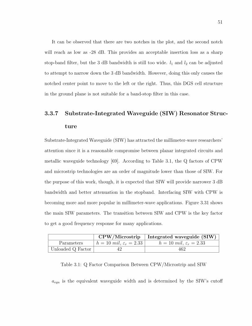
3.3.7 Substrate-Integrated Waveguide (SIW) Resonator Structure . 51
4 UWB Antenna in Coplanar Waveguide (CPW) Technology 58
4.1 Coplanar Waveguide (CPW) UWB Antenna . . . . . . . . . . . . . . 58
4.2 Coplanar Waveguide (CPW) UWB Antenna With Band-stop Filter . 66
4.2.1 Design of The CPW UWB Antenna With Band-stop Filter . . 66
4.2.2 Measurement of CPW UWB Antenna With Band-stop Filter . 74
5 Conclusions 83

vi
Bibliography 85
A Ultra-Wideband (UWB Technology) Enabling High-speed Wire-
less Personal Area Networks 94
vii
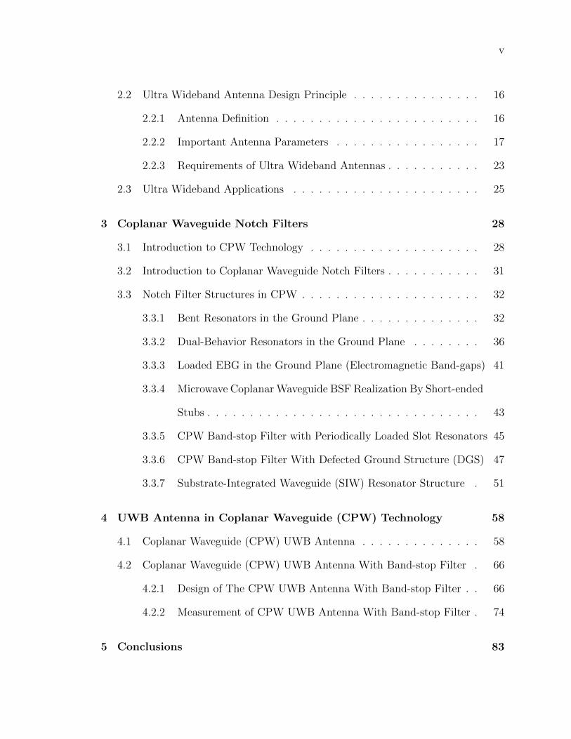
List of Tables
Table 3.1 Q Factor Comparison Between CPW/Microstrip and SIW . . . 51
Table 3.2 Initial Dimensions for The SIW Structure . . . . . . . . . . . . . 54
Table 3.3 Initial Dimensions for The SIW Structure With New Transition 55
Table 3.4 Optimized Dimensions for The SIW Structure With New Transition 56
Table 3.5 Structure Comparison . . . . . . . . . . . . . . . . . . . . . . . 57
Table 4.1 Dimensions of The CPW Antenna . . . . . . . . . . . . . . . . . 58
Table 4.2 Dimensions of The UWB Antenna and The Filter . . . . . . . . 66
Table 4.3 Simulated Frequencies . . . . . . . . . . . . . . . . . . . . . . . 71
viii
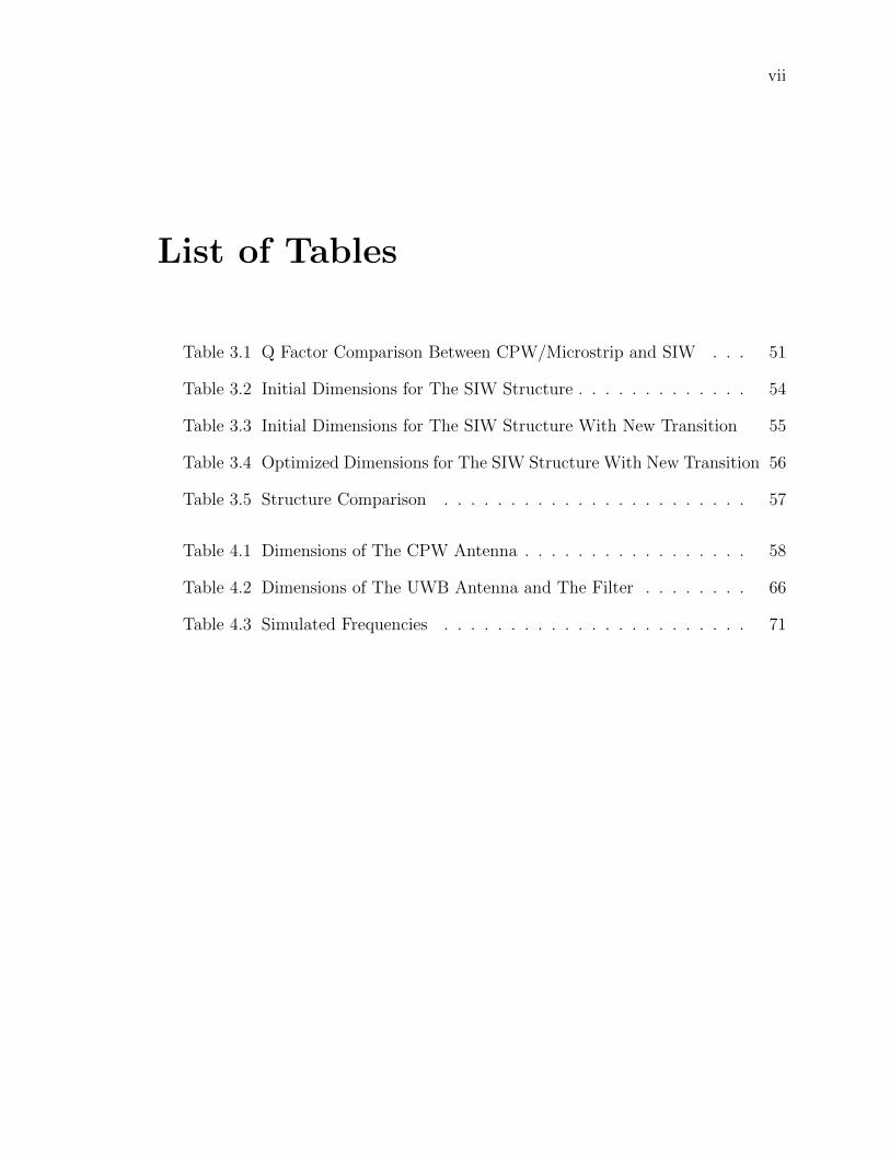
List of Figures
Figure 2.1 (a) Lodge’s Triangular Bow-Tie Antenna [43] (b) Lodge’s Bi-
Conical Antenna [43] . . . . . . . . . . . . . . . . . . . . . . . . 11
Figure 2.2 (a) Carter’s Bi-Conical Antenna [44] (b) Carter’s Conical Monopole
[44] . . . . . . . . . . . . . . . . . . . . . . . . . . . . . . . . . 11
Figure 2.3 Schelkunoff’s Spherical Dipole [1] . . . . . . . . . . . . . . . . . 12
Figure 2.4 (a) Lindenblad’s Element [1] (b) Lindenblad’s Turnstile Array [1] 12
Figure 2.5 (a) Brillouin’s Omni-Directional Coxial Horn [46] (b) Brillouin’s
Directional Coaxial Horn [46] . . . . . . . . . . . . . . . . . . . 13
Figure 2.6 (a) King’s Conical Horn [47] (b) Katzin’s Rectangular Horn [48] 13
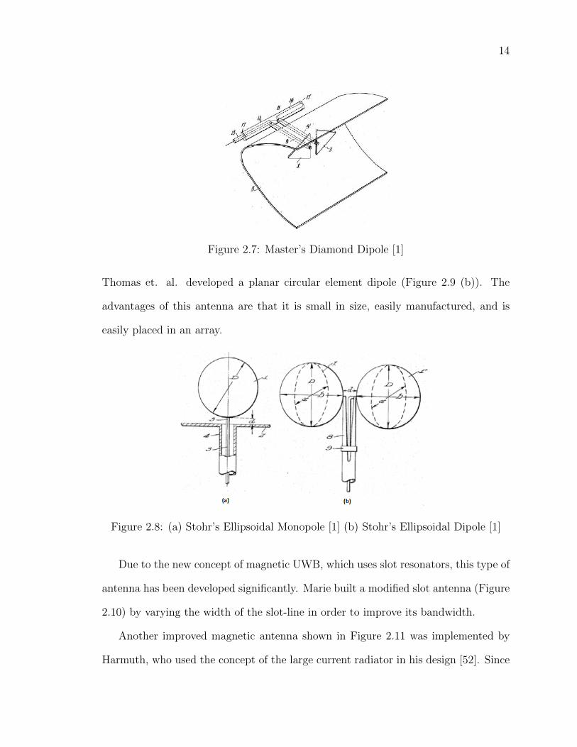
Figure 2.7 Master’s Diamond Dipole [1] . . . . . . . . . . . . . . . . . . . 14
Figure 2.8 (a) Stohr’s Ellipsoidal Monopole [1] (b) Stohr’s Ellipsoidal Dipole
[1] . . . . . . . . . . . . . . . . . . . . . . . . . . . . . . . . . . 14
Figure 2.9 (a) Lalezaris’ Broadband Notch Antenna [1] (b) Thomas et al’s
Circular Element Dipole [1] . . . . . . . . . . . . . . . . . . . . 15
Figure 2.10 Marie’s Wide Band Slot Antenna [1] . . . . . . . . . . . . . . . 15
Figure 2.11 Harmuth’s Large Current Radiator [1] . . . . . . . . . . . . . . 16
Figure 2.12 Barne’s UWB Slot Antenna [1] . . . . . . . . . . . . . . . . . . 16
Figure 2.13 Antenna Principle [53] . . . . . . . . . . . . . . . . . . . . . . . 17
Figure 2.14 Antenna Radiation Pattern [53] . . . . . . . . . . . . . . . . . 18
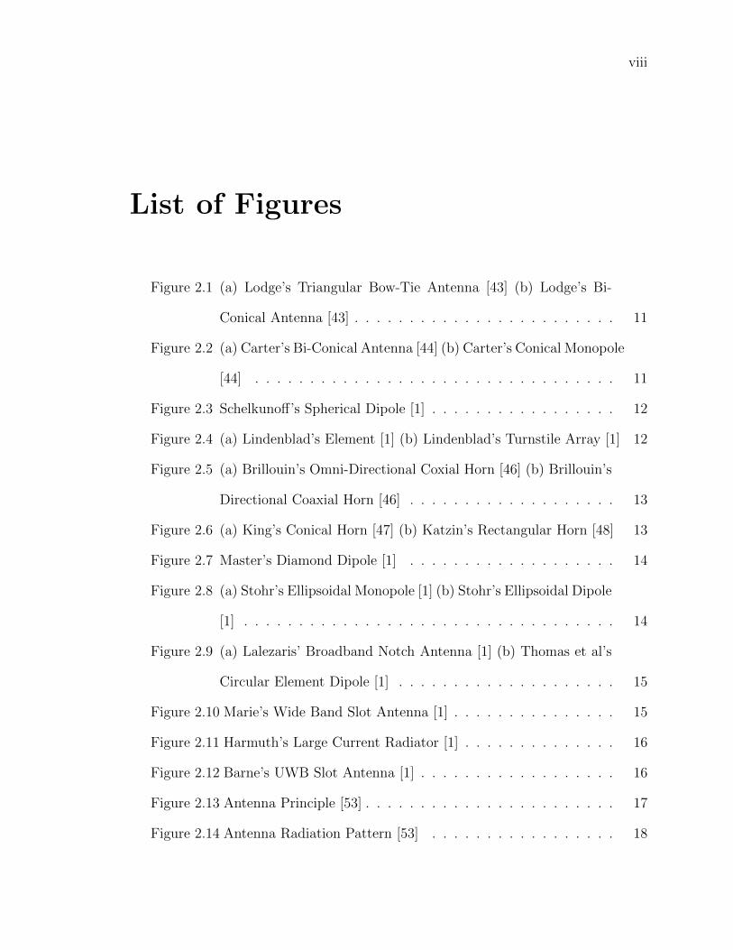
ix
Figure 2.15 Co-ordinate System Transformation Between Cartesian and Spher-
ical Coordinates [53] . . . . . . . . . . . . . . . . . . . . . . . . 19
Figure 2.16 Radiation Plane [53] . . . . . . . . . . . . . . . . . . . . . . . . 19
Figure 2.17 Common Radiation Patterns [53] . . . . . . . . . . . . . . . . . 20
Figure 2.18 Antenna Directivity [53] . . . . . . . . . . . . . . . . . . . . . . 21
Figure 2.19 (a) Antenna Transmitting Mode (b) Antenna Receiving Mode
[53] . . . . . . . . . . . . . . . . . . . . . . . . . . . . . . . . . 22
Figure 2.20 PC and Its Peraphicals (c.f.Appendix) . . . . . . . . . . . . . . 26
Figure 2.21 WPAN (c.f.Appendix) . . . . . . . . . . . . . . . . . . . . . . . 26
Figure 3.1 General CPW Structure [65] . . . . . . . . . . . . . . . . . . . . 29
Figure 3.2 Electric and Magnetic Fields in CPW [65] . . . . . . . . . . . . 29
Figure 3.3 Cross-section Dimensions of The CPW Structure [65] . . . . . . 30
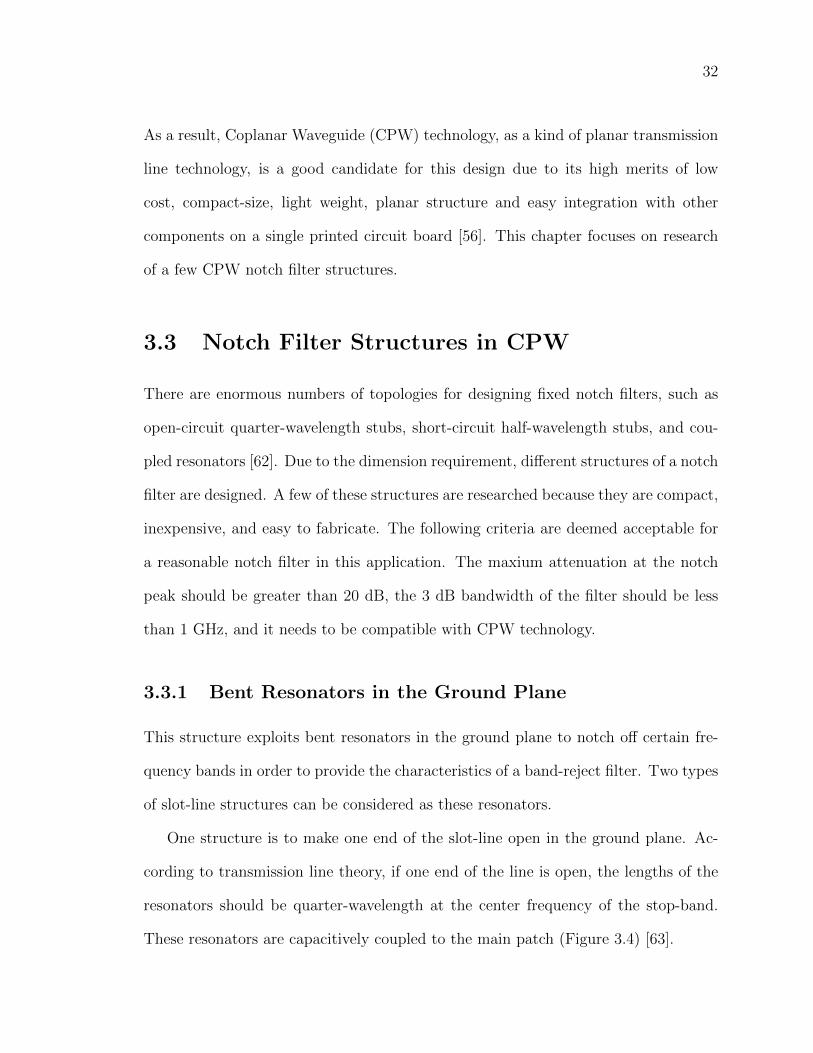
Figure 3.4 Bend Resonators With Open Structure . . . . . . . . . . . . . . 33
Figure 3.5 Effective Permittivity for The Bend Resonator With Open Struc-
ture . . . . . . . . . . . . . . . . . . . . . . . . . . . . . . . . . 34
Figure 3.6 Frequency Response for The Bend Resonator With Open Structure 34
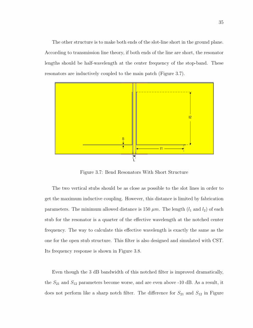
Figure 3.7 Bend Resonators With Short Structure . . . . . . . . . . . . . . 35
Figure 3.8 Frequency Response for The Bend Resonator With Short Structure 36
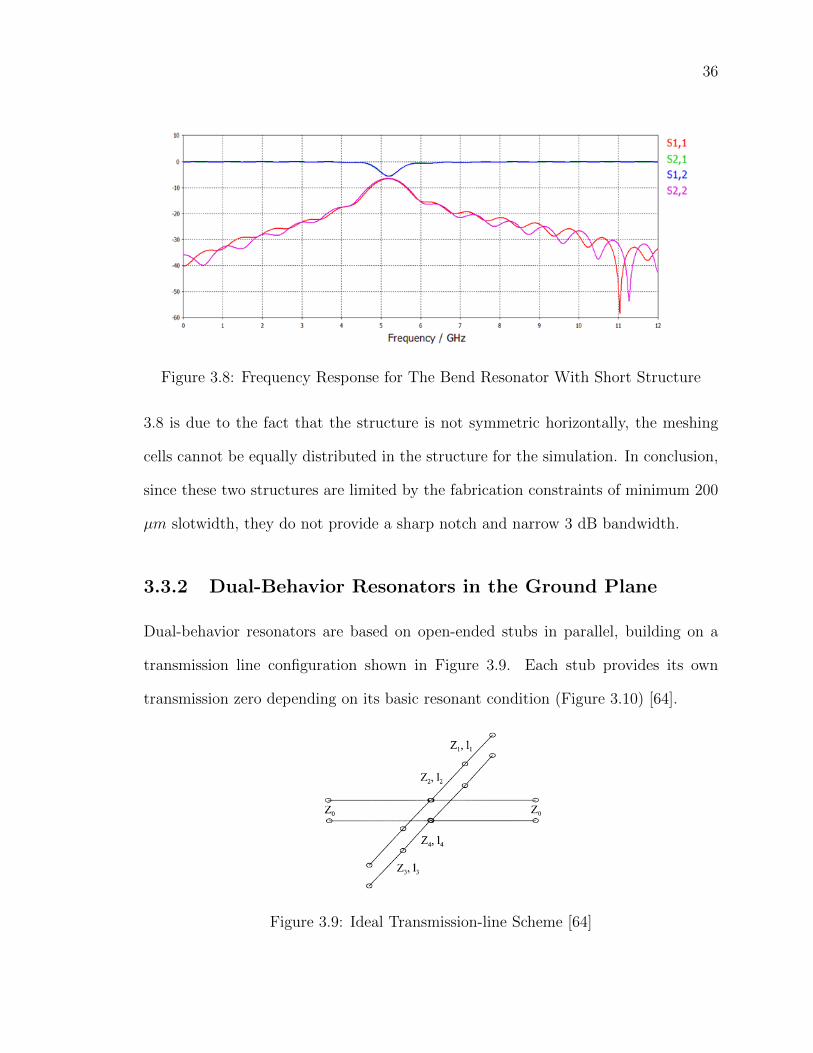
Figure 3.9 Ideal Transmission-line Scheme [64] . . . . . . . . . . . . . . . . 36
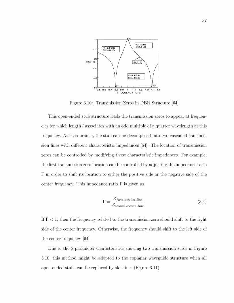
Figure 3.10 Transmission Zeros in DBR Structure [64] . . . . . . . . . . . . 37
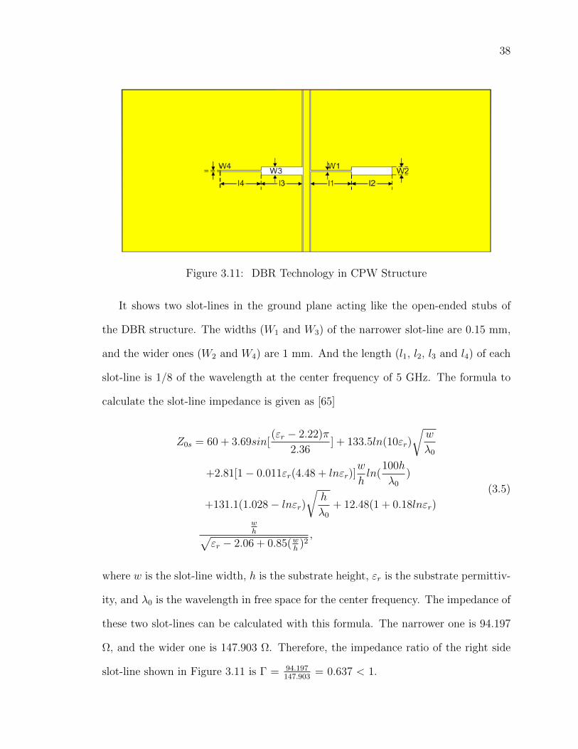
Figure 3.11 DBR Technology in CPW Structure . . . . . . . . . . . . . . . 38
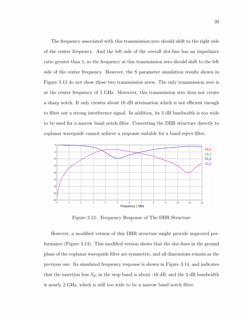
Figure 3.12 Frequency Response of The DBR Structure . . . . . . . . . . . 39
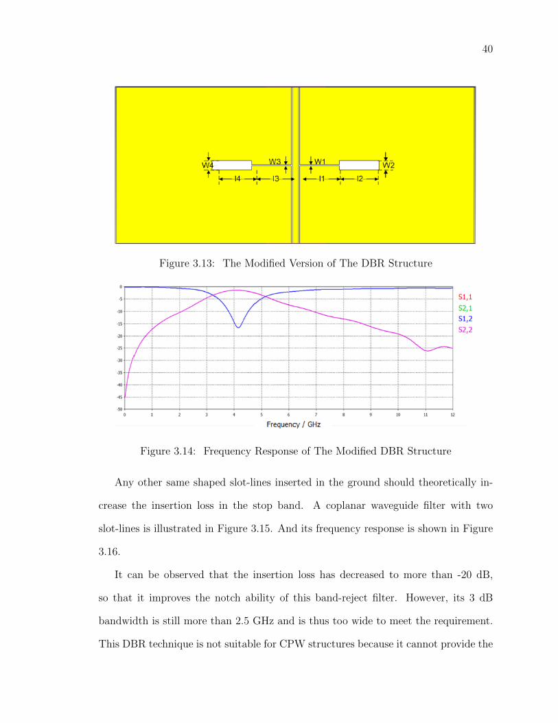
Figure 3.13 The Modified Version of The DBR Structure . . . . . . . . . . 40
Figure 3.14 Frequency Response of The Modified DBR Structure . . . . . . 40
x
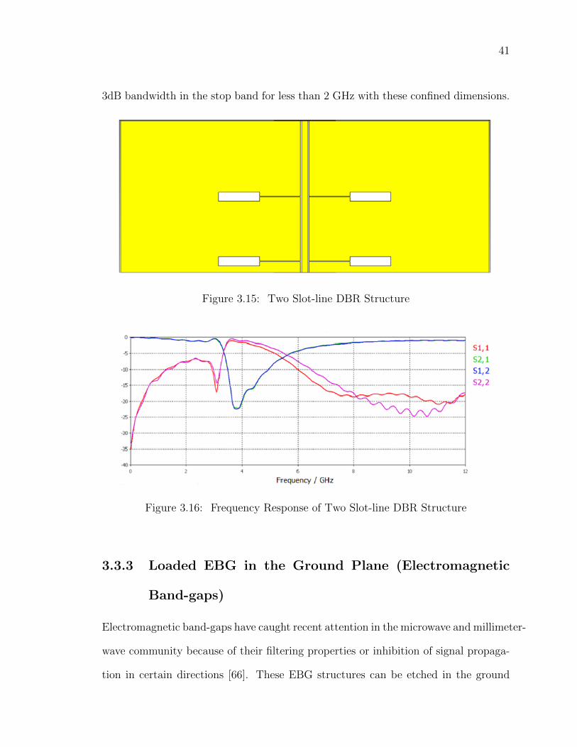
Figure 3.15 Two Slot-line DBR Structure . . . . . . . . . . . . . . . . . . . 41
Figure 3.16 Frequency Response of Two Slot-line DBR Structure . . . . . . 41
Figure 3.17 Loaded EBG Structure . . . . . . . . . . . . . . . . . . . . . . 42
Figure 3.18 Equivalent Circuit of The Loaded EBG Structure [66] . . . . . 42
Figure 3.19 Frequency Response of The Loaded EBG Structure . . . . . . 43
Figure 3.20 BSF With Short Stubs . . . . . . . . . . . . . . . . . . . . . . 44
Figure 3.21 Frequency Response of The BSF With Short Stubs . . . . . . . 44
Figure 3.22 BSF With Periodically Loaded Slot Resonators [67] . . . . . . 45
Figure 3.23 Equivalent Circuit of a BSF With Periodically Loaded Slot Res-
onators [67] . . . . . . . . . . . . . . . . . . . . . . . . . . . . . 46
Figure 3.24 Frequency Response of a BSF With Periodically Loaded Slot
Resonators . . . . . . . . . . . . . . . . . . . . . . . . . . . . . 46
Figure 3.25 Band-stop Filter With DGS Structure . . . . . . . . . . . . . . 47
Figure 3.26 Frequency Response of A BSF With DGS Structure . . . . . . 48
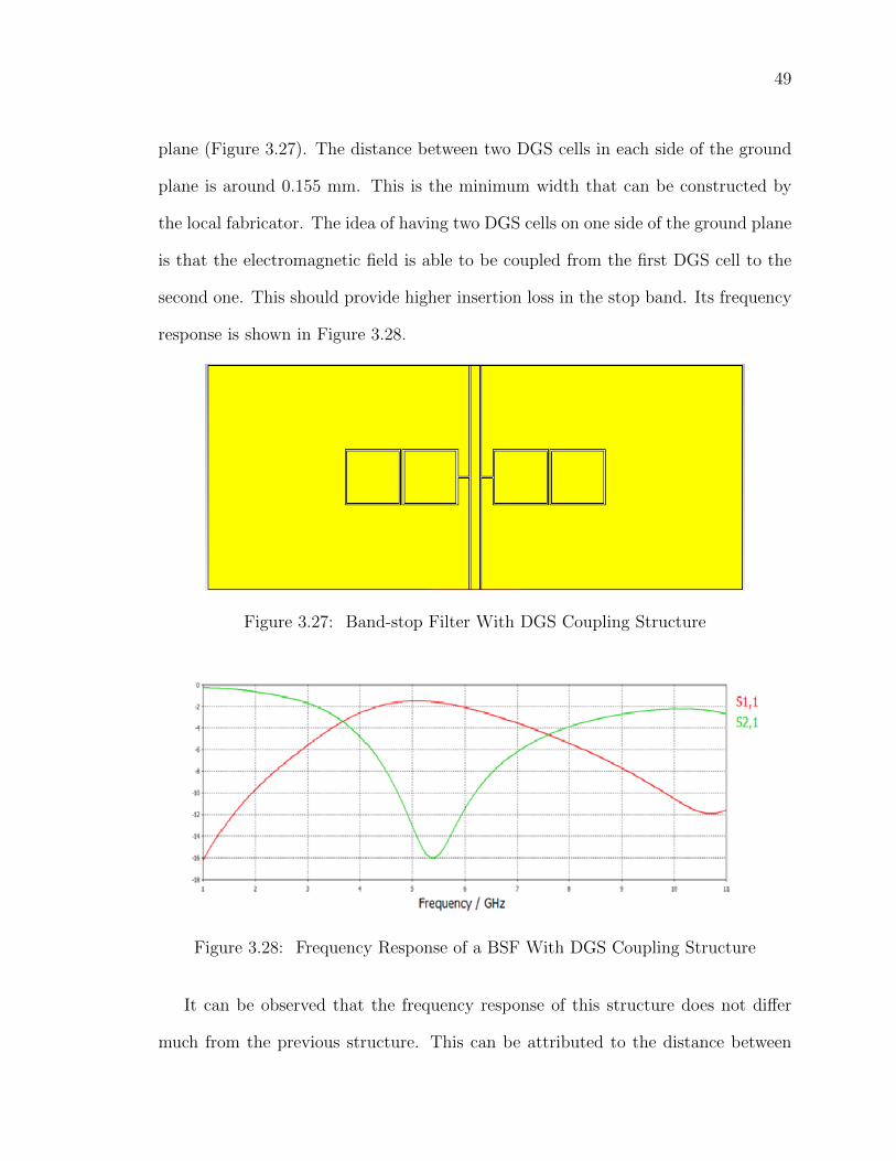
Figure 3.27 Band-stop Filter With DGS Coupling Structure . . . . . . . . 49
Figure 3.28 Frequency Response of a BSF With DGS Coupling Structure . 49
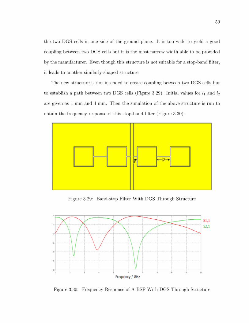
Figure 3.29 Band-stop Filter With DGS Through Structure . . . . . . . . . 50
Figure 3.30 Frequency Response of A BSF With DGS Through Structure . 50
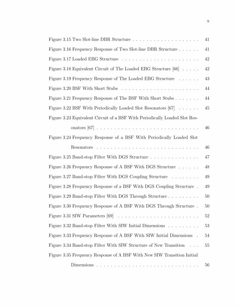
Figure 3.31 SIW Parameters [69] . . . . . . . . . . . . . . . . . . . . . . . 52
Figure 3.32 Band-stop Filter With SIW Initial Dimensions . . . . . . . . . 53
Figure 3.33 Frequency Response of A BSF With SIW Initial Dimensions . 54
Figure 3.34 Band-stop Filter With SIW Structure of New Transition . . . 55
Figure 3.35 Frequency Response of A BSF With New SIW Transition Initial
Dimensions . . . . . . . . . . . . . . . . . . . . . . . . . . . . . 56
xi
Figure 3.36 Frequency Response of A BSF With New SIW Transition Opti-
mized Dimensions . . . . . . . . . . . . . . . . . . . . . . . . . 56
Figure 4.1 CPW UWB Antenna Without The Band-stop Filter [72] . . . . 59
Figure 4.2 Input Time-domain Signal . . . . . . . . . . . . . . . . . . . . . 60
Figure 4.3 Amplitude of The Input Signal . . . . . . . . . . . . . . . . . . 60
Figure 4.4 Phase of The Input Signal . . . . . . . . . . . . . . . . . . . . . 61
Figure 4.5 Return Loss of The UWB Antenna . . . . . . . . . . . . . . . . 61
Figure 4.6 Time-domain Output Signal of The UWB Antenna (note that
Eφ is below 0.06 V/m) . . . . . . . . . . . . . . . . . . . . . . . 62
Figure 4.7 Output Signal Amplitude of The UWB Antenna . . . . . . . . 63
Figure 4.8 Output Signal Phase of The UWB Antenna . . . . . . . . . . . 63
Figure 4.9 Gain of The UWB Antenna . . . . . . . . . . . . . . . . . . . . 64
Figure 4.10 H-plane Radiation Patterns of The UWB Antenna; (a) Co-
polarization, (b) Cross-polarization . . . . . . . . . . . . . . . . 64
Figure 4.11 E-plane Radiation Pattern of The UWB Antenna; (a) Co-polarization,
(b) Cross-polarization . . . . . . . . . . . . . . . . . . . . . . . 65
Figure 4.12 Group Delay of The UWB Antenna . . . . . . . . . . . . . . . 66
Figure 4.13 CPW UWB Antenna With Stop-band Filter . . . . . . . . . . 67
Figure 4.14 Frequency Response of The CPW UWB Antenna With Initial
Dimensions . . . . . . . . . . . . . . . . . . . . . . . . . . . . . 68
Figure 4.15 Frequency Response of The CPW UWB Antenna With Opti-
mized Dimensions . . . . . . . . . . . . . . . . . . . . . . . . . 68
Figure 4.16 Output Signal of The CPW UWB Antenna With BSF . . . . . 69
xii
Figure 4.17 Amplitude of The Output Signal for The CPW UWB Antenna
With BSF . . . . . . . . . . . . . . . . . . . . . . . . . . . . . . 70
Figure 4.18 Phase of The Output Signal for The CPW UWB Antenna With
BSF . . . . . . . . . . . . . . . . . . . . . . . . . . . . . . . . . 70
Figure 4.19 Gain of This CPW UWB Antenna . . . . . . . . . . . . . . . . 71
Figure 4.20 H-plane Radiation Patterns of The UWB Antenna With Band-
stop Filter; (a) Co-polarization, (b) Cross-polarization . . . . . 72
Figure 4.21 E-plane Radiation Patterns of The UWB Antenna With Band-
stop Filter, (a) Co-polarization, (b) Cross-polarization . . . . . 73
Figure 4.22 Group Delay for The CWP UWB Antenna with BSF . . . . . 73
Figure 4.23 (a) Antenna’s Front View (b) Antenna’s Back View . . . . . . 74
Figure 4.24 (a) Schematic View (b) Measurement Setup . . . . . . . . . . . 75
Figure 4.25 S11 Comparison between Measurement and Simulation . . . . . 75
Figure 4.26 Anechoic Chamber View . . . . . . . . . . . . . . . . . . . . . 76
Figure 4.27 (a) Schematic View (b) Measurement Setup (c) AUT Setup . . 77
Figure 4.28 H-plane and E-plane Radiation Patterns Measurement of The
UWB Antenna With Band-stop Filter at 4.3GHz; (a) H-plane
Co-polarization, (b) H-plane Cross-polarization, (c) E-plane Co-
polarization, (d) E-plane Cross-polarization . . . . . . . . . . . 78
Figure 4.29 H-plane and E-plane Radiation Patterns Measurement of The
UWB Antenna With Band-stop Filter at 5GHz; (a) H-plane
Co-polarization, (b) H-plane Cross-polarization, (c) E-plane Co-
polarization, (d) E-plane Cross-polarization . . . . . . . . . . . 79
xiii
Figure 4.30 H-plane and E-plane Radiation Patterns Measurement of The
UWB Antenna With Band-stop Filter at 7GHz; (a) H-plane
Co-polarization, (b) H-plane Cross-polarization, (c) E-plane Co-
polarization, (d) E-plane Cross-polarization . . . . . . . . . . . 80
Figure 4.31 H-plane and E-plane Radiation Patterns Measurement of The
UWB Antenna With Band-stop Filter at 9GHz; (a) H-plane
Co-polarization, (b) H-plane Cross-polarization, (c) E-plane Co-
polarization, (d) E-plane Cross-polarization . . . . . . . . . . . 81
Figure 4.32 H-plane and E-plane Radiation Patterns Measurement of The
UWB Antenna With Band-stop Filter at 10GHz; (a) H-plane
Co-polarization, (b) H-plane Cross-polarization, (c) E-plane Co-
polarization, (d) E-plane Cross-polarization . . . . . . . . . . . 82
xiv
List of Acronyms
AUT Antenna Under Test
BSF Band-stop Filter
CPW Co-planar Waveguide
CST Computer Simulation Technology
DBR Dual-behavior Resonator
DGB Defected Ground Plane
DSR Dual-spiral-shaped Slot Resonator
EBG Electromagnetic Band-gap
FCC Federal Communications Commission
HDTV High-definition TV
HIPERLAN High Performance Local Area Network
IEEE Institute of Electrical and Electronics Engineers
LPI Low Probability of Interception and Detection
MESFET Metal-semiconductor Field Effect Transistor
MMIC Monolithic Microwave Integrated Circuit
NBI Narrow-band Interferences
PC Personal Computer
xv
PCB Printed Circuit Board
PDA Personal Digital Assistant
SIW Substrate Integrated Waveguide
SNR Signal-to-noise Ratio
STB Set-top Box
TEM Transverse ElectroMagnetic
UWB Ultra Wideband
VSWR Voltage Standing Wave Ratio
Wi-Fi Wireless Fidelity
WLAN Wireless Local Area Network
WPAN Wireless Personal Area Network
xvi
ACKNOWLEDGEMENTS
This thesis is the accomplishment of two years of research and experiment whereby
I have been helped and supported by many people. Here and now, I am honored to
express my appreciation to all of them.
The first person I would like to thank is my supervisor, Prof. Jens Bornemann.
Under these years learning from Prof. Jens Bornemann, I have found he is knowl-
edgeable, compassionate and friendly. I owe him a great deal of appreciation for his
tireless guidance through the research, for his patience and support.
I would like to thank Farzaneh Taringou for her help in understanding CST simu-
lation software and modeling of the proposed UWB antenna. Special thanks to Lisa
Locke for being there when I needed her advice. I would also like to thank Mr. Ian
Wood for performing CST simulation results on the proposed notch filter as part to
confirm its validation. The work would not have been accomplished without the help
from my fellow colleagues and friends. I appreciate them all for many discussions and
having strong confidence in me.
Last, but not lease, my truehearted appreciation goes to my family for their caring,
understanding and encouragement throughout my research.
Chapter 1
Introduction
The rapid development of modern telecommunication systems has dramatically in-
creased the interest in enlarging the transmission bandwidth. As a result, components
and systems for ultra wideband (UWB) technology have been performing a very im-
perative role in the telecommunication research community. Designing and testing a
UWB application is at the forefront of research and development in this area. Within
such a system, the UWB antenna is an important component because its transmit-
ting and receiving properties are different from those for conventional narrowband
operation. Many UWB antennas have been developed. TEM horns can be used for
localized equipment, whereas printed-circuit antennas are more practical for mobile
communication [1].
With the release of the 3.1-10.6 GHz band for UWB communication, a number of
diversified UWB applications are invented, such as imaging systems, ground penetrat-
ing surveillance systems, vehicular radar systems, communications, and measurements
systems, etc. Portable handhelds for short-range and large bandwidth communica-
2
tion will be involved in future UWB systems. The implementation of UWB antennas
in printed-circuit technologies within a relatively small area is more than necessary.
Nowadays, a variety of UWB antennas with either microstrip, e.g. [2]-[11] or coplanar
waveguide feeds, e.g [12]-[27], and in combined technologies, e.g. [28][29] have been
designed, mainly for the 3.1-10.6 GHz band, and for high frequency ranges, e.g. [30],
and lower frequency ranges, e.g. [31], as well.
In addition, these UWB antennas need a band-rejection filter to avoid interference
with existing wireless networks such as IEEE 802.11a in USA (5.15-5.35 GHz, 5.725-
5.825 GHz) and HIPERLAN/2 in Europe (5.15-5.35 GHz, 5.47-5.725 GHz) [32]-[35].
To avoid adding new circuits to the communication system, band-notching techniques
can be applied directly to various UWB planar antennas. One possibility is to load the
UWB antenna with two SIW resonators in the ground plane, their center frequency
being at the peak of the stop band.
1.1 Purpose of Thesis
Coplanar waveguide technology provides a great deal of advantages for the fabrica-
tion of printed-circuit UWB antennas. This technology only requires both the ground
plane and antenna patch on the same side of the substrate, whereas microstrip tech-
nology applied to these antennas requires metallization patterns on both sides of the
substrate. In this case, easier fabrication can be achieved with coplanar waveguide
technology. Furthermore, UWB antennas with coplanar waveguide technology can
provide wideband characteristics, and bidirectional radiation patterns similar to a
microstrip feed.
3
The purpose of this thesis is to design a coplanar UWB antenna with a band-stop
filter and use some commercially available electromagnetic field solvers to simulate
this antenna’s characteristics and performance. Through the design process, the
finite-integration full wave solver CST Microwave Studio is employed for analysis
purpose and for final optimization according to the voltage-standing wave ratio and
radiation pattern behaviors. To validate the results, CST simulation results are an-
alyzed first, and then a fabricated sample antenna is measured. It verifies that the
simulated results agree well with the measured ones.
1.2 Contributions
The contributions of this research are twofold:
First, a new printed-circuit co-planar waveguide band-stop filter in substrate
waveguide technology is presented. Its performance demonstrates that it is more
suitable than other structures published so far.
Second, a printed-circuit UWB antenna in coplanar technology combined with
a band-stop filter has a contribution of avoiding the interference from other wire-
less communication networks. It divides the entire band into multiple sub-bands. It
makes this antenna application more practical than other designs published so far.
4
1.3 Thesis Overview
Chapter 2 of this thesis is an introduction to UWB development and provides ba-
sic knowledge about UWB antenna design. Every sub-section of Chapter 2 contains
information based on one or two references. The major content is quite similar to
these references, with changes only in wordings and phrases. This chapter introduces
history and fundamentals of UWB technology. It offers background information and
presents UWB applications.
Chapter 3 gives detailed information about research in different structures of
a band-stop filter. And it shows the comparison of all simulated results of these
structures. After these results are compared, it illustrates the reasons for choosing
substrate integrated waveguide technology (SIW) for this band-stop filter. In addi-
tion, it provides the detailed mathematical calculation and design parameters of using
SIW technology.
Chapter 4 presents a new printed-circuit UWB antenna in CPW technology
combined with the above SIW band-stop filter. The first part shows the simulation
results of this CPW UWB antenna alone in CST. Next, after the band-stop filter is
integrated with the antenna, the entire antenna simulation results are presented. A
comparison of the simulation results between the antenna alone and the combined
application is demonstrated as well. Finally, experimental results demonstrate the
validity of the design process.
5
Chapter 5 summarizes the most important accomplishments throughout the the-
sis.
6
Chapter 2
Fundamentals of Ultra Wideband
Technology
Ultra Wideband technology has come to be realized since the 1960s. It is defined
through utilizing carrier-free, impulse, baseband, time domain, nonsinusoidal and
large-relative-bandwidth radio/radar signals. The benefits of carrier-free are that a
transmitting signal does not need the analog modulating stage, and a receiving signal
does not need the analog demodulating stage. Because of this, the mixing stage in
a tranceiver is not necessary any more. This will reduce the design complexity of
the analog circuit. The basic concept of developing ultra wideband is to transmit
and receive a number of extremely short pulses at ultra low power, besides being
extremely compact and inexpensive [36]. The duration of one pulse is typically a few
tens of picoseconds to a few nanoseconds. These pulses represent one or a few cycles
of an RF carrier waveform. As a result, the resulting waveforms can achieve extremely
broadband signals. Due to the difficulty of determining the actual RF fundamental
frequency for an extremely short pulse, the term carrier-free is used [37]. The FCC has
7
recently authorized Ultra-Wideband (UWB) communication between 3.1 GHz and
10.6 GHz; it has a bandwidth equal to or larger than 20% of the center frequency,
or has a bandwidth equal to or greater than 500 MHz [38]. Moreover, it allows
UWB devices to share the spectrum with existing radio services as long as emission
restrictions, in the form of a spectral mask, are met. Its power spectral density
emission limit for UWB transmitters is -41.3 dBm/MHz, equal to 75 nanowatts/MHz
[39]. It indicates that the UWB signal provides very low power spectral density, which
causes the maximum transmitting power to be a few milliwatts. It guarantees that
these spectral power densities are well below a receiver noise level.
Advantages of UWB technology are:
• The FCC requires that the transmitting power for UWB systems is -41.3 dBm/MHz.
It puts them in the category of unintentional radiators, such as TVs and com-
puter monitors. This power limitation restricts UWB systems to stay below the
noise floor of a typical narrowband receiver. With this regulation, UWB systems
are able to coexist with current radio services with minimal or no interference
[39].
• It provides a large bandwidth in UWB systems so that the channel capacity is
improved. Channel capacity, or data rate in a digital system, is defined as the
maximum amount of information being able to be transmitted per second over
a communication channel. There is a channel capacity of a UWB system since
Hartley-Shannon’s capacity formula depends on the system’s bandwidth. It is
given by
C = B · log2(1 + SNR), (2.1)
where C is the maximum channel capacity, B indicates the system bandwidth,
8
and the SNR is the signal-to-noise ratio. From the above equation, channel
capacity linearly increases with the bandwidth. Since UWB signals occupy
several gigahertz of bandwidth, it leads the data rate to be gigabits per second.
This makes UWB systems a perfect candidate for short-range, high-data-rate
wireless applications such as wireless personal area networks (WPANs) [39].
• Eqn 2.1 also shows that the channel capacity logarithmically depends on signal-
to-noise ratio (SNR). It implies that UWB communications systems are able to
work in harsh communication channels with low SNRs and still provide a large
channel capacity due to their large bandwidth [39].
• Since UWB communications systems have low average power transmission, it
is extremely difficult to detect and intercept their signals. Furthermore, UWB
pulses are time modulated with unique codes for each transceiver pair. The
time modulation of very narrow pulses makes UWB systems more secure to
transmit because detecting a picosecond pulse, without knowing when it will
come, is nearly impossible. Thus, UWB systems can achieve high security, low
probability of interception and detection communications. This is a mandatory
attribute for military operations [39].
9
2.1 Development of Ultra Wideband Technology
and Antennas
2.1.1 History of Ultra Wideband Technology
In the late 1950’s, an effort was made to develop a phased array radar system in the
Lincoln Laboratory. This radar system employed two Butler Hybrid Phasing Matrices
which were an interconnection of 3 dB branch line couplers to form a 2-N port network.
Due to the demand of understanding the wideband properties of this network, studies
were deployed to investigate the properties of the four-port interconnection of quarter-
wave TEM-mode lines forming the branch line coupler. Such studies did not exist
at that time. It began with the analysis of a general microwave 2-N port as a bi-
conjugate network. The impulse response of this network was a pulse train and equally
spaced [36]. From this point in time, ultra wideband (UWB) became a new branch of
research in the field of time-domain electromagnetics [40]. At the same time, Oliver
invented a sampling oscilloscope, and he used avalanche transistors and tunnel diodes
to generate the short pulses [36]. The impulse response of the above networks could
be monitored and measured. From this point, the development of short pulse radar
and communications systems had begun. In the late 1960s, Ross and Robbins at the
Sperry Research Center implemented a few radar and communication applications
by using this impulse response method [41]. In 1973, the first UWB communications
application was invented as a short-pulse receiver by Ross.
Through the late 1980s, this ultra wideband technology was named baseband,
carrier-free or impulse generation technology until approximately 1989, when the
U.S. Department of Defense announced it as “ultra wideband”. By that time, the
10
UBW theory had existed for 30 years. Therefore, quite a few techniques and many
applications about it had been developed. In addition, over 50 patents had been
awarded to Sperry for his contributions in the fields of UWB pulse generation and
reception methods, and applications such as communications, radar, automobile col-
lision avoidance radar, positioning systems, liquid level sensing and altimetry [42].
Prior to 1994, researches and development in UWB technology, especially in the
field of impulse communications, were regulated by the U.S. Government. Since 1994,
the U.S. government loosened the classification restrictions on the UWB fields, so a
number of works could be accomplished [42].
2.1.2 Development of Ultra Wideband Antenna
The first proposal of ultra-wideband antennas presented the idea of narrowband fre-
quency domain radio. In 1898, the concept of “syntony” was introduced by Oliver
Lodge. This idea was to tune a transmitter and a receiver to the same frequency in
order to maximize the receiving signal [43]. Using this idea, he came up with a variety
of “capacity areas”, and these capacity areas were later called antennas. Lodge made
a significant contribution in the antenna development because he invented spherical
dipoles, square plate dipoles, bi-conical dipoles, and triangular or “bow-tie” dipoles.
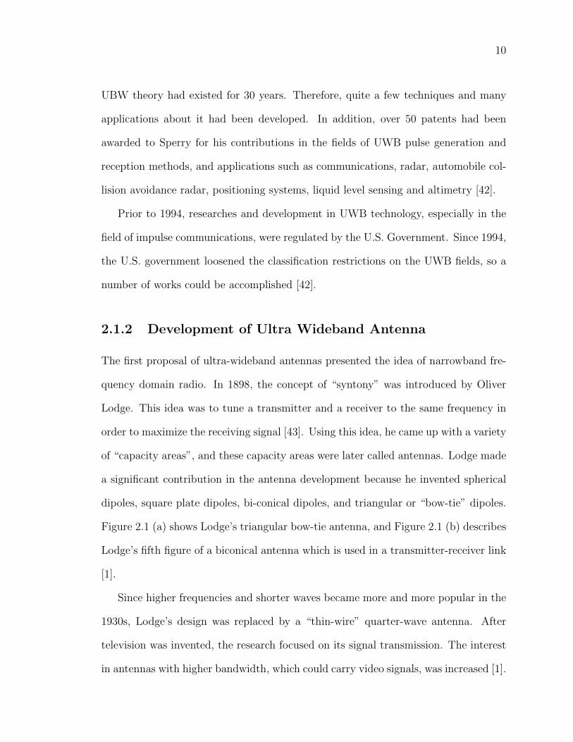
Figure 2.1 (a) shows Lodge’s triangular bow-tie antenna, and Figure 2.1 (b) describes
Lodge’s fifth figure of a biconical antenna which is used in a transmitter-receiver link
[1].
Since higher frequencies and shorter waves became more and more popular in the
1930s, Lodge’s design was replaced by a “thin-wire” quarter-wave antenna. After
television was invented, the research focused on its signal transmission. The interest
in antennas with higher bandwidth, which could carry video signals, was increased [1].
11
Figure 2.1: (a) Lodge’s Triangular Bow-Tie Antenna [43] (b) Lodge’s Bi-ConicalAntenna [43]
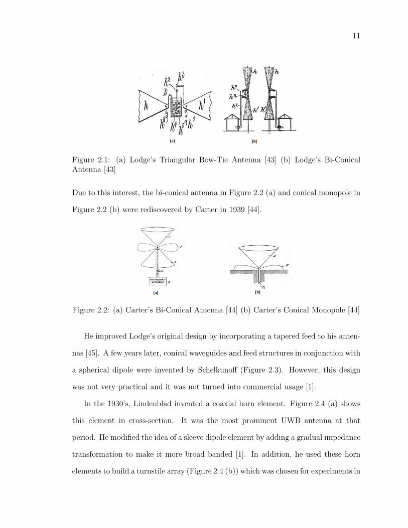
Due to this interest, the bi-conical antenna in Figure 2.2 (a) and conical monopole in
Figure 2.2 (b) were rediscovered by Carter in 1939 [44].
Figure 2.2: (a) Carter’s Bi-Conical Antenna [44] (b) Carter’s Conical Monopole [44]
He improved Lodge’s original design by incorporating a tapered feed to his anten-
nas [45]. A few years later, conical waveguides and feed structures in conjunction with
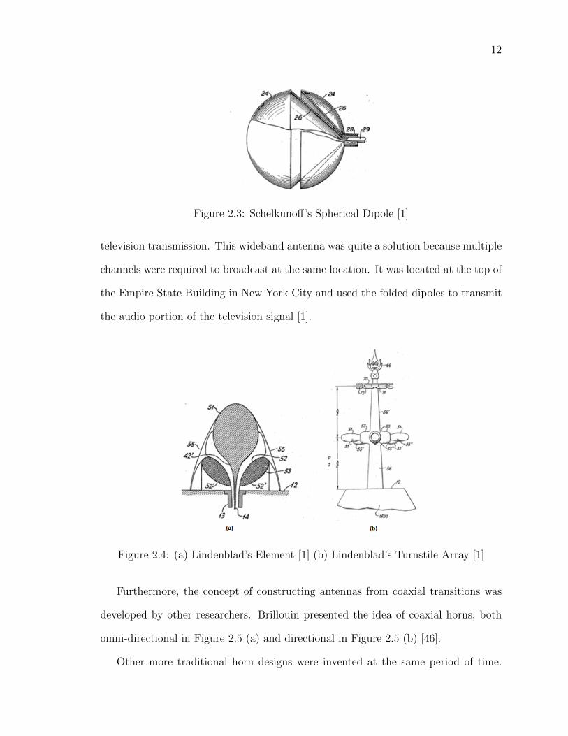
a spherical dipole were invented by Schelkunoff (Figure 2.3). However, this design
was not very practical and it was not turned into commercial usage [1].
In the 1930’s, Lindenblad invented a coaxial horn element. Figure 2.4 (a) shows
this element in cross-section. It was the most prominent UWB antenna at that
period. He modified the idea of a sleeve dipole element by adding a gradual impedance
transformation to make it more broad banded [1]. In addition, he used these horn
elements to build a turnstile array (Figure 2.4 (b)) which was chosen for experiments in
12
Figure 2.3: Schelkunoff’s Spherical Dipole [1]
television transmission. This wideband antenna was quite a solution because multiple
channels were required to broadcast at the same location. It was located at the top of
the Empire State Building in New York City and used the folded dipoles to transmit
the audio portion of the television signal [1].
Figure 2.4: (a) Lindenblad’s Element [1] (b) Lindenblad’s Turnstile Array [1]
Furthermore, the concept of constructing antennas from coaxial transitions was
developed by other researchers. Brillouin presented the idea of coaxial horns, both
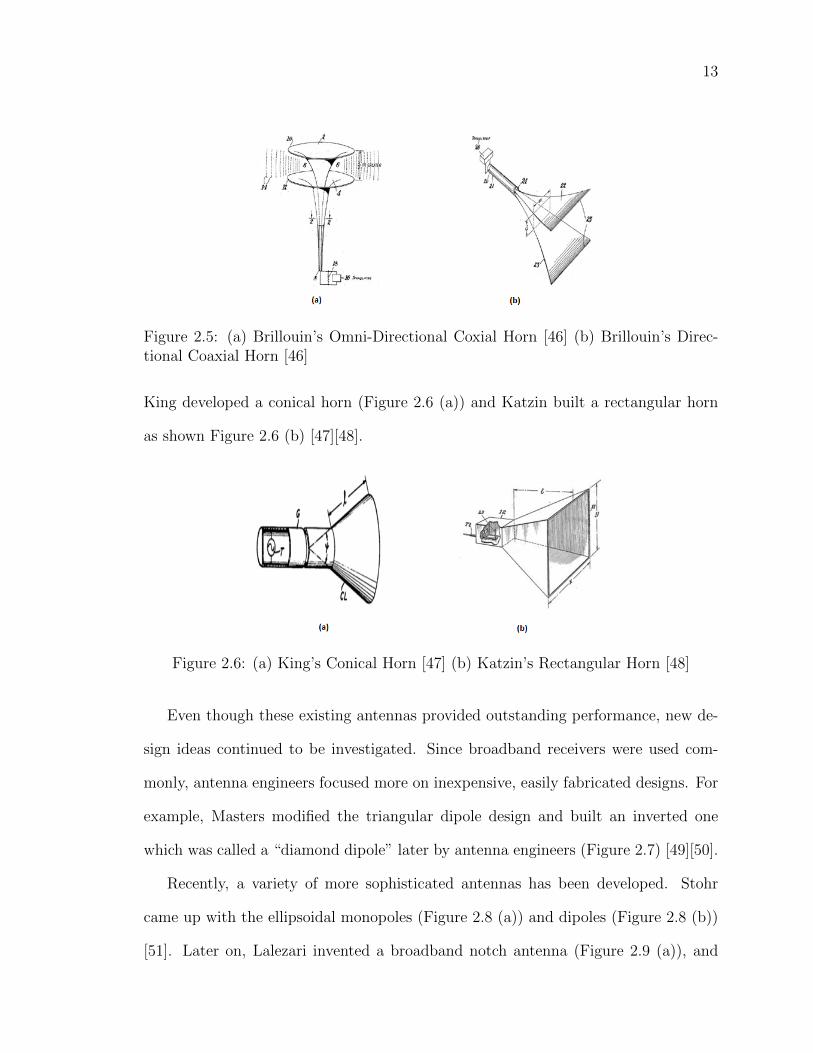
omni-directional in Figure 2.5 (a) and directional in Figure 2.5 (b) [46].
Other more traditional horn designs were invented at the same period of time.
13
Figure 2.5: (a) Brillouin’s Omni-Directional Coxial Horn [46] (b) Brillouin’s Direc-tional Coaxial Horn [46]
King developed a conical horn (Figure 2.6 (a)) and Katzin built a rectangular horn
as shown Figure 2.6 (b) [47][48].
Figure 2.6: (a) King’s Conical Horn [47] (b) Katzin’s Rectangular Horn [48]
Even though these existing antennas provided outstanding performance, new de-
sign ideas continued to be investigated. Since broadband receivers were used com-
monly, antenna engineers focused more on inexpensive, easily fabricated designs. For
example, Masters modified the triangular dipole design and built an inverted one
which was called a “diamond dipole” later by antenna engineers (Figure 2.7) [49][50].
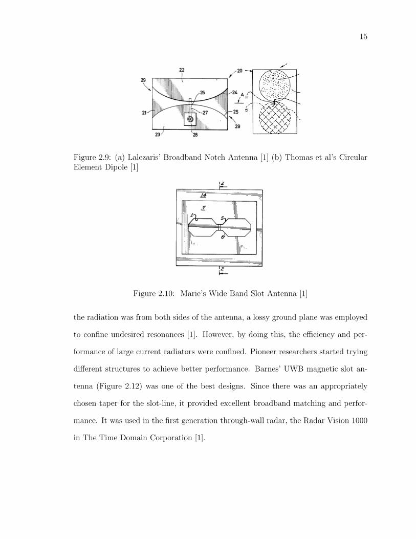
Recently, a variety of more sophisticated antennas has been developed. Stohr
came up with the ellipsoidal monopoles (Figure 2.8 (a)) and dipoles (Figure 2.8 (b))
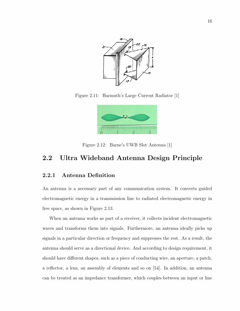
[51]. Later on, Lalezari invented a broadband notch antenna (Figure 2.9 (a)), and
14
Figure 2.7: Master’s Diamond Dipole [1]
Thomas et. al. developed a planar circular element dipole (Figure 2.9 (b)). The
advantages of this antenna are that it is small in size, easily manufactured, and is
easily placed in an array.
Figure 2.8: (a) Stohr’s Ellipsoidal Monopole [1] (b) Stohr’s Ellipsoidal Dipole [1]
Due to the new concept of magnetic UWB, which uses slot resonators, this type of
antenna has been developed significantly. Marie built a modified slot antenna (Figure
2.10) by varying the width of the slot-line in order to improve its bandwidth.
Another improved magnetic antenna shown in Figure 2.11 was implemented by
Harmuth, who used the concept of the large current radiator in his design [52]. Since
15
Figure 2.9: (a) Lalezaris’ Broadband Notch Antenna [1] (b) Thomas et al’s CircularElement Dipole [1]
Figure 2.10: Marie’s Wide Band Slot Antenna [1]
the radiation was from both sides of the antenna, a lossy ground plane was employed
to confine undesired resonances [1]. However, by doing this, the efficiency and per-
formance of large current radiators were confined. Pioneer researchers started trying
different structures to achieve better performance. Barnes’ UWB magnetic slot an-
tenna (Figure 2.12) was one of the best designs. Since there was an appropriately
chosen taper for the slot-line, it provided excellent broadband matching and perfor-
mance. It was used in the first generation through-wall radar, the Radar Vision 1000
in The Time Domain Corporation [1].
16
Figure 2.11: Harmuth’s Large Current Radiator [1]
Figure 2.12: Barne’s UWB Slot Antenna [1]
2.2 Ultra Wideband Antenna Design Principle
2.2.1 Antenna Definition
An antenna is a necessary part of any communication system. It converts guided
electromagnetic energy in a transmission line to radiated electromagnetic energy in
free space, as shown in Figure 2.13.
When an antenna works as part of a receiver, it collects incident electromagnetic
waves and transforms them into signals. Furthermore, an antenna ideally picks up
signals in a particular direction or frequency and suppresses the rest. As a result, the
antenna should serve as a directional device. And according to design requirement, it
should have different shapes, such as a piece of conducting wire, an aperture, a patch,
a reflector, a lens, an assembly of elements and so on [54]. In addition, an antenna
can be treated as an impedance transformer, which couples between an input or line
17
Figure 2.13: Antenna Principle [53]
impedance and the impedance of free space [55]. A sophisticated antenna design is
able to meet the system specifications and improve overall performance.
2.2.2 Important Antenna Parameters
The performance and the characteristics of an antenna depend on a variety of param-
eters including radiation pattern, directivity, gain, input impedance etc.
1. Radiation Pattern
Radiation pattern is a mathematical function or graphical representation of
the radiation properties of an antenna. It can indicate the field strength and
radiation intensity. It is always measured in the far-field region because the
spatial distribution is independent on radial distance. The radiation pattern in
the far-field region is a function of a particular position along the path or surface
of constant radius and is represented as a two dimensional or three dimensional
graph. Figure 2.14 demonstrates a radiation pattern example of a Hertzian
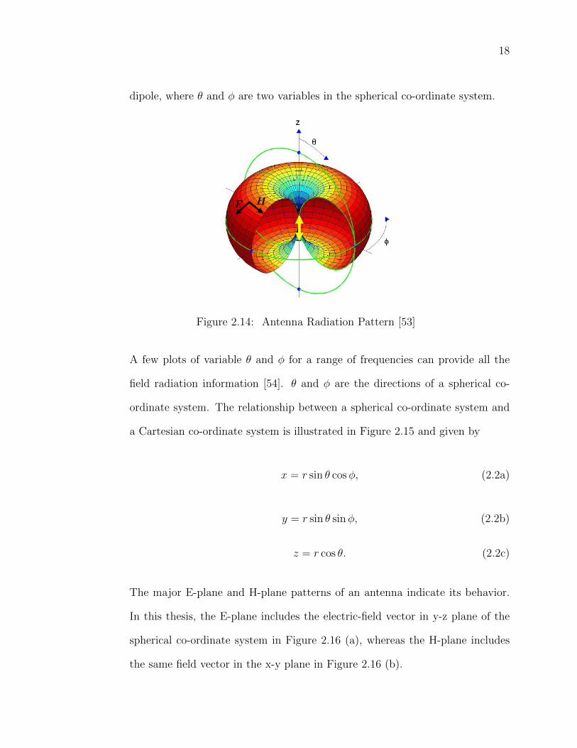
18
dipole, where θ and φ are two variables in the spherical co-ordinate system.
Figure 2.14: Antenna Radiation Pattern [53]
A few plots of variable θ and φ for a range of frequencies can provide all the
field radiation information [54]. θ and φ are the directions of a spherical co-
ordinate system. The relationship between a spherical co-ordinate system and
a Cartesian co-ordinate system is illustrated in Figure 2.15 and given by
x = r sin θ cosφ, (2.2a)
y = r sin θ sinφ, (2.2b)
z = r cos θ. (2.2c)
The major E-plane and H-plane patterns of an antenna indicate its behavior.
In this thesis, the E-plane includes the electric-field vector in y-z plane of the
spherical co-ordinate system in Figure 2.16 (a), whereas the H-plane includes
the same field vector in the x-y plane in Figure 2.16 (b).
19
Figure 2.15: Co-ordinate System Transformation Between Cartesian and SphericalCoordinates [53]
Figure 2.16: Radiation Plane [53]
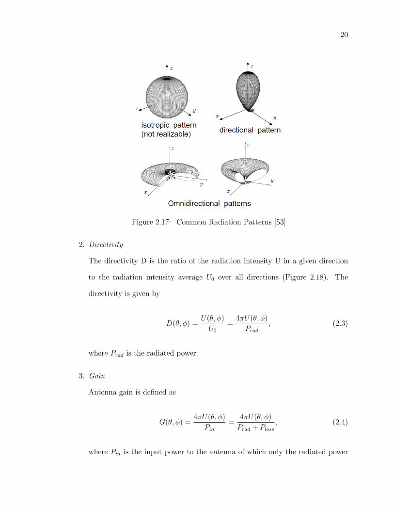
There are three commonly used radiation patterns shown in Figure 2.17. They
are isotropic, directional, and omnidirectional patterns. Note that the isotropic
radiator is used only as the theoretical stardard to measure directivity in deciBel
over isotropic (dBi).
20
Figure 2.17: Common Radiation Patterns [53]
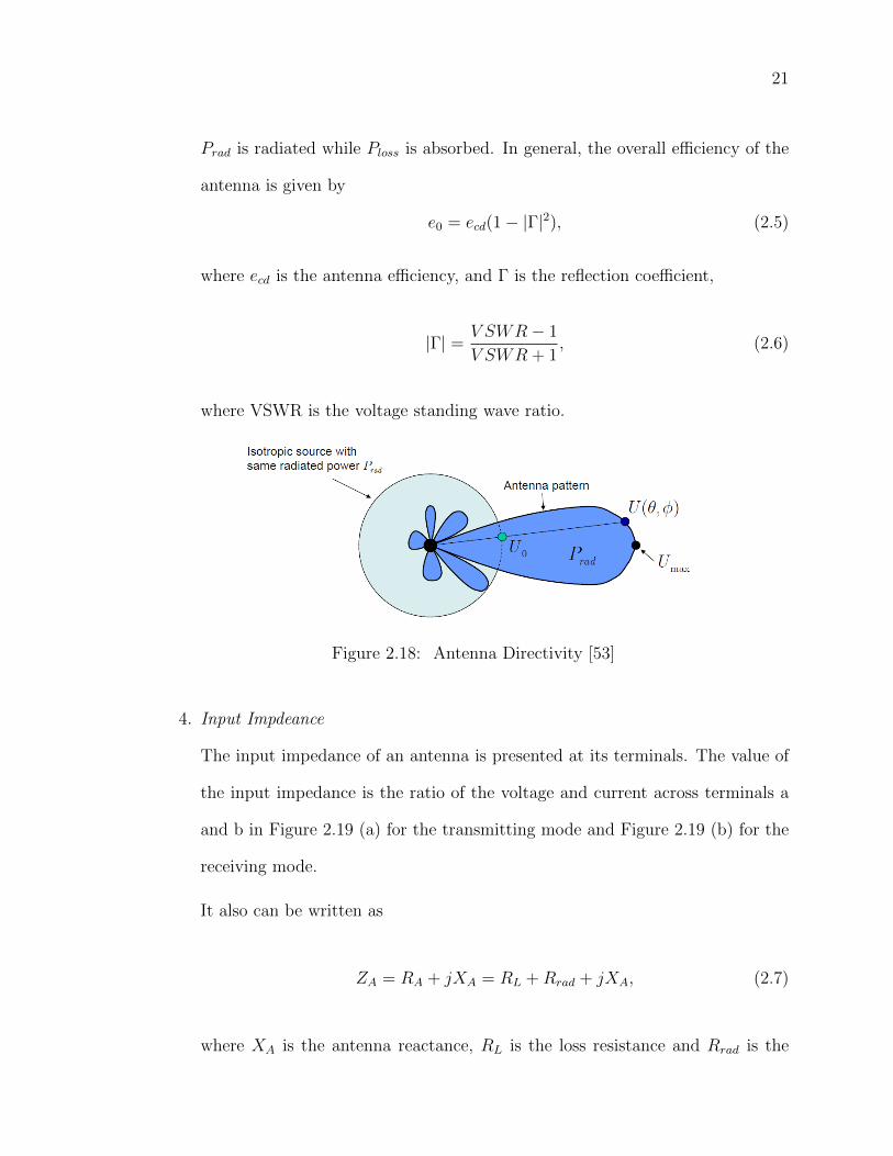
2. Directivity
The directivity D is the ratio of the radiation intensity U in a given direction
to the radiation intensity average U0 over all directions (Figure 2.18). The
directivity is given by
D(θ, φ) =U(θ, φ)
U0
=4πU(θ, φ)
Prad, (2.3)
where Prad is the radiated power.
3. Gain
Antenna gain is defined as
G(θ, φ) =4πU(θ, φ)
Pin=
4πU(θ, φ)
Prad + Ploss, (2.4)
where Pin is the input power to the antenna of which only the radiated power
21
Prad is radiated while Ploss is absorbed. In general, the overall efficiency of the
antenna is given by
e0 = ecd(1− |Γ|2), (2.5)
where ecd is the antenna efficiency, and Γ is the reflection coefficient,
|Γ| = V SWR− 1
V SWR + 1, (2.6)
where VSWR is the voltage standing wave ratio.
Figure 2.18: Antenna Directivity [53]
4. Input Impdeance
The input impedance of an antenna is presented at its terminals. The value of
the input impedance is the ratio of the voltage and current across terminals a
and b in Figure 2.19 (a) for the transmitting mode and Figure 2.19 (b) for the
receiving mode.
It also can be written as
ZA = RA + jXA = RL +Rrad + jXA, (2.7)
where XA is the antenna reactance, RL is the loss resistance and Rrad is the
22
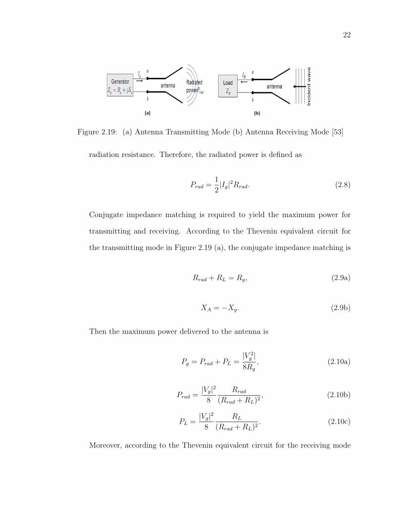
Figure 2.19: (a) Antenna Transmitting Mode (b) Antenna Receiving Mode [53]
radiation resistance. Therefore, the radiated power is defined as
Prad =1
2|Ig|2Rrad. (2.8)
Conjugate impedance matching is required to yield the maximum power for
transmitting and receiving. According to the Thevenin equivalent circuit for
the transmitting mode in Figure 2.19 (a), the conjugate impedance matching is
Rrad +RL = Rg, (2.9a)
XA = −Xg. (2.9b)
Then the maximum power delivered to the antenna is
Pg = Prad + PL =|V 2g |
8Rg
, (2.10a)
Prad =|Vg|2
8
Rrad
(Rrad +RL)2, (2.10b)
PL =|Vg|2
8
RL
(Rrad +RL)2. (2.10c)
Moreover, according to the Thevenin equivalent circuit for the receiving mode

23
in 2.19 (b), the conjugate impedance matching is
Rrad +RL = RR, (2.11a)
XA = −XR. (2.11b)
The maximum power received at the load of the antenna is
PR =|VR|2
2| RR
4(Rrad +RL)2| = |VR|
2
8| 1
Rrad +RL
| = |VR|2
8RR
, (2.12a)
Prad =|Vg|2
8
Rrad
(Rrad +RL)2, (2.12b)
PL =|Vg|2
8
RL
(Rrad +RL)2. (2.12c)
2.2.3 Requirements of Ultra Wideband Antennas
UWB communication techniques have received a great amount of attention from
both academia and industry in the past few years because of the high merit of their
advantages. All wireless systems and applications including UWB designs need a
means of transferring energy or signals from the apparatus, which is an antenna,
to free space in the form of electromagnetic waves or vice versa. An antenna has
been recognized as a critical element of a successful design of any wireless device
since wireless systems are highly dependent on their antenna characteristics. Based
on that, UWB antennas have become an important and active area of research and
have presented antenna engineers with major design challenges [56]. Antennas play
crucial roles in either conventional wireless or UWB wireless systems. Due to the
strong commercial demand of ultra-wideband systems, their antenna designs have
24
been regaining interest in recent years. However, designing a UWB antenna presents
more challenges than designing a conventional one because a UWB antenna is required
to receive all frequencies in the wide band at the same time. As a result, the behavior
and performance of a UWB antenna should be consistent and predictable across the
entire bandwidth [55].
The main challenge is the extremely wide bandwidth. A UWB antenna is fun-
damentally different from a narrow band antenna since its frequency bandwidth is
ultra wide. The FCC requires a UWB antenna to be capable of providing an absolute
wide frequency band of at least 500MHz. It should perform consistently across the
entire frequency bandwidth. This requires that the antenna radiation pattern, gain
and impedance matching must be stable over the whole bandwidth [54]. In some
cases, since other narrow band devices and services occupy a portion of this ultra
wide band, a UWB antenna should be able to yield the band-rejection features to
prevent the interference from those devices and services [57][58].
The second challenge is that the directivity of an antenna is either directional or
omni-directional, depending on application. If it is a mobile or a hand-held device,
an omni-directional radiation pattern is required. On the other hand, if it is a radar
system or a high gain directional system, a directional radiation pattern is required
[54].
The third challenge is the size of a UWB antenna. Due to the usage of a suitable
antenna in a mobile or a portable device, it must be compatable with integration on
a printed circuit board (PCB).
The fourth challenge is to achieve good time domain performance for a UWB
antenna. Unlike a conventional system transmitting information by a carrier wave, a
UWB system directly employs extremely short pulses for data transmission. In other
25
words, the ultra-wide frequency band should be occupied [54]. Due to this enormous
operating bandwidth, a crucial impact on the transmitted and received waveforms is
imposed by the UWB antenna. A good time domain performance, such as minimizing
pulse distortion, is a primary requirement of a suitable UWB antenna because the
signal waveform is the carrier of useful data information [54].
2.3 Ultra Wideband Applications
Ultra wideband technology, well-known for its high data throughput, low probability
of interception and detection, multipath immunity, precision ranging and location,
has been considered for a diversity of applications which include both wireless com-
munications and radar systems [42].
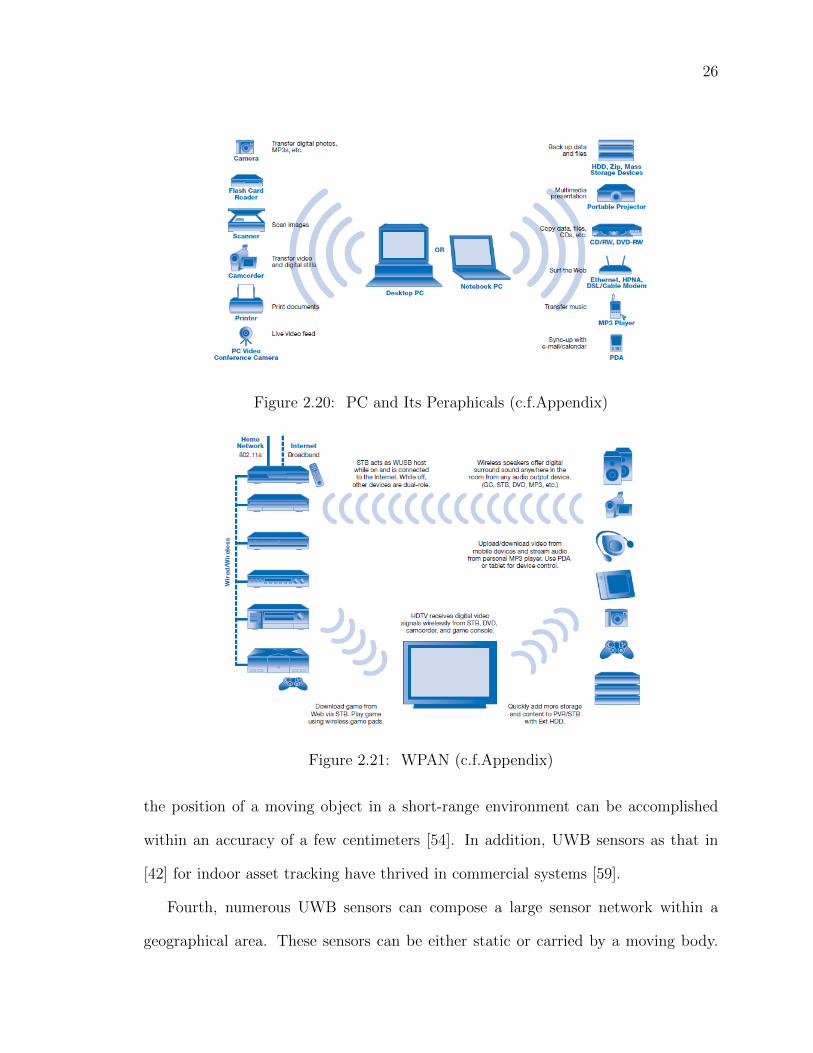
First, UWB technology provides a solution for the band-width, cost, power con-
sumption, and physical size requirements for consumer electronic devices. By using
this technology, Personal Computers (PCs) are able to connect to all their wireless
PC peripherals such as personal digital recorders, MP3 recorders and players, digital
cameras, etc., as seen in Figure 2.20.
Second, with UWB technology, high-definition TVs (HDTVs), set-top boxes (STBs),
gaming systems, personal digital assistants (PDAs), and cell phones are able to con-
nect to each other in a wireless personal area network (WPAN) in a digital home as
shown in Figure 2.21.
Third, due to the high data rate characteristic, UWB systems are able to collect,
propagate or exchange information in a very short time period. As a result, higher
accuracy for short-range UWB positioning and tracking systems can be achieved.
For example, with the advanced tracking mechanism in [42], precisely determining
26
Figure 2.20: PC and Its Peraphicals (c.f.Appendix)
Figure 2.21: WPAN (c.f.Appendix)
the position of a moving object in a short-range environment can be accomplished
within an accuracy of a few centimeters [54]. In addition, UWB sensors as that in
[42] for indoor asset tracking have thrived in commercial systems [59].
Fourth, numerous UWB sensors can compose a large sensor network within a
geographical area. These sensors can be either static or carried by a moving body.
27
When they are applied for securing homes, tracking and monitoring, or mobile, these
sensors can be installed on soldiers, firemen, automobiles, or robots in military and
emergency response situations [60]. UWB systems have operated in a variety of
difficult situations in order to provide faster and more accurate communications. For
example, they are used to search for people or objects in a collapsed building after
an earthquake, children lost in a playground, injured athletes in remote places, fire
fighters in a burning building and so on [54].
Fifth, UWB applications also include radar systems. It was originally applied
in military services and later for commercial usage. For example, the Hummingbird
system is a radar application for the U.S. Naval Air Systems Command and is shown
in [42]. It utilizes the high data rate characteristic to determine the altitude precisely,
and avoid collision [42].
Another application of short range radar operating in the X-band region of the
spectrum is also presented in [42]. This radar was deployed for the U.S. Army Missile
Command as a low probability of interception and detection (LPI/D), anti-jam, radar
proximity sensor for caliber, small caliber and submunition applications. This system
has a center frequency of 10 GHz with a 2.5 GHz operating band. This application
was specially designed for short range (less than 6 feet), and the resolution distance
of these UWB sensors was 6 inches. Due to its average output power of less than 85
nanowatts, this radar was capable of detecting a -4 dB per m2 target in a range of
approximately 15 feet with a small, micro-strip patch antenna [42]. The usage of UWB
is everywhere, such as mobile phones, medical applications, satellite communications,
etc.
28
Chapter 3
Coplanar Waveguide Notch Filters
3.1 Introduction to CPW Technology
The CPW was invented by Wen in 1969 [65]. This structure includes a strip of
metallic film deposited on the top of a dielectric substrate with two ground planes at
each side of the strip as shown in Figure 3.1. The original idea was that the thickness
of the substrate be infinite. However, that cannot be practically implemented. Thus,
the thickness of the substrate becomes finite and needs to be large enough so that all
the electric and magnetic fields can taper to zero inside the substrate. In addition,
the width of the ground plane should be as small as possible if the CPW is mounted
in monolithic microwave integrated circuits (MMICs).
The electric and magnetic field distribution of the CPW structure are shown in
Figure 3.2. It demonstrates that not all the fields are contained in the dielectric
substrate. Some of them are in the substrate, and the others are in open air. It
causes the analysis of the CPW structure to be quasi-static. The full-wave analysis of
the CPW is involved to investigate the phase velocity and characteristic impedance

29
Figure 3.1: General CPW Structure [65]
Figure 3.2: Electric and Magnetic Fields in CPW [65]
associated with frequencies. The quasi-static formulas for calculating the effective
dielectric constant (εre), the phase velocity (υph), and the characteristic impedance
(Z0cp) are given by [65]
εre = 1 +εr − 1
2
K(k4)
K ′(k4)
K ′(k3)
K(k3), (3.1a)
υph =c√εre, (3.1b)
30
Z0cp =30π√εre
K ′(k3)
K(k3), (3.1c)
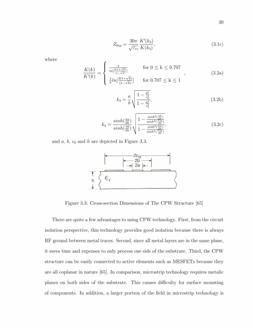
where
K(k)
K ′(k)=
π
ln[2(1+
√k)
(1−√k)
]for 0 ≤ k ≤ 0.707
1πln[2(1+
√k)
(1−√k)
] for 0.707 ≤ k ≤ 1
, (3.2a)
k3 =a
b
√√√√1− b2
c20
1− a2
c20
, (3.2b)
k4 =sinh(πa
2h)
sinh(πb2h
)
√√√√√1− sinh2(πb2h
)
sinh2(πc02h
)
1− sinh2(πa2h
)
sinh2(πc02h
)
, (3.2c)
and a, b, c0 and h are depicted in Figure 3.3.
Figure 3.3: Cross-section Dimensions of The CPW Structure [65]
There are quite a few advantages to using CPW technology. First, from the circuit
isolation perspective, this technology provides good isolation because there is always
RF ground between metal traces. Second, since all metal layers are in the same plane,
it saves time and expenses to only process one side of the substrate. Third, the CPW
structure can be easily connected to active elements such as MESFETs because they
are all coplanar in nature [65]. In comparison, microstrip technology requires metalic
planes on both sides of the substrate. This causes difficulty for surface mounting
of components. In addition, a larger portion of the field in microstrip technology is
31
contained in the substrate which causes increased losses. With these advantages, the
antenna in this thesis adopts the CPW structure.
3.2 Introduction to Coplanar Waveguide Notch Fil-
ters
A UWB wireless system employs signals with a bandwidth spectrum of 3.1-10.6 GHz
and transmits the signal at a high transmission speed of 100-480 Mbps. It enables
transmission at a higher speed than conventional WLAN such as Wi-Fi at a speed of
54 Mbps. Due to the characteristic of low energy per pulse, UWB systems are subject
to high level narrow-band interferences (NBI) even though UWB systems may enjoy
a high spreading gain due to the large bandwidths. Specially, IEEE 802.11a systems
operate around 5 GHz, which overlap the band of UWB signals regulated by the FCC,
and will bring significant interference to UWB systems. If such interference is not
suppressed properly, the UWB receiver will not function well. Thus, it is necessary
to employ a band-stop filter to offer rejection ability in a band from 5 to 6 GHz. One
solution to this specification is to design a notch filter after the receiving antenna
to provide an appropriate rejection at the required frequency range [61]. There are
numerous types of notch filters attached to antenna structures in modern wireless
communication systems. However, the trend of designing such a filter and antenna
is to utilize a planar waveguide structure in the UWB system because this filter in
combination with this antenna should be small enough to build on small, low-profile
integrated circuits in order to be compatible with portable electronic devices. The
purpose of a planar design is to miniaturize the volume of the UWB antenna and filter.
Furthermore, its two dimensional (2D) geometry makes the fabrication relatively easy.
32
As a result, Coplanar Waveguide (CPW) technology, as a kind of planar transmission
line technology, is a good candidate for this design due to its high merits of low
cost, compact-size, light weight, planar structure and easy integration with other
components on a single printed circuit board [56]. This chapter focuses on research
of a few CPW notch filter structures.
3.3 Notch Filter Structures in CPW
There are enormous numbers of topologies for designing fixed notch filters, such as
open-circuit quarter-wavelength stubs, short-circuit half-wavelength stubs, and cou-
pled resonators [62]. Due to the dimension requirement, different structures of a notch
filter are designed. A few of these structures are researched because they are compact,
inexpensive, and easy to fabricate. The following criteria are deemed acceptable for
a reasonable notch filter in this application. The maxium attenuation at the notch
peak should be greater than 20 dB, the 3 dB bandwidth of the filter should be less
than 1 GHz, and it needs to be compatible with CPW technology.
3.3.1 Bent Resonators in the Ground Plane
This structure exploits bent resonators in the ground plane to notch off certain fre-
quency bands in order to provide the characteristics of a band-reject filter. Two types
of slot-line structures can be considered as these resonators.
One structure is to make one end of the slot-line open in the ground plane. Ac-
cording to transmission line theory, if one end of the line is open, the lengths of the
resonators should be quarter-wavelength at the center frequency of the stop-band.
These resonators are capacitively coupled to the main patch (Figure 3.4) [63].
33
Figure 3.4: Bend Resonators With Open Structure
The length (l1 and l2) of each section is one eighth of the effective wavelength at 5
GHz. Two of them connecting like an L shape form a bent resonator. The substrate
used here is RT/Duroid 6002 (εr = 2.94). The dimensions of L and S are 0.7 mm
and 0.2 mm, respectively. This leads to a characteristic impedance of Z0 equal 70.8
Ω. The effective wavelength λeff is given as
λeff =λfree√εre
=c
fcenter√εre, (3.3)
where c is the speed of light in free space, fcenter is the center frequency of the stop
band, and εre is the substrate effective relative permittivity at this center frequency.
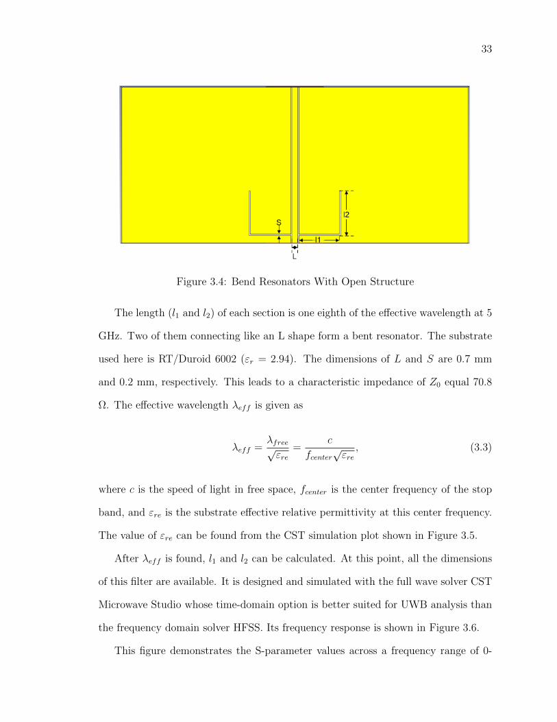
The value of εre can be found from the CST simulation plot shown in Figure 3.5.
After λeff is found, l1 and l2 can be calculated. At this point, all the dimensions
of this filter are available. It is designed and simulated with the full wave solver CST
Microwave Studio whose time-domain option is better suited for UWB analysis than
the frequency domain solver HFSS. Its frequency response is shown in Figure 3.6.
This figure demonstrates the S-parameter values across a frequency range of 0-

34
Figure 3.5: Effective Permittivity for The Bend Resonator With Open Structure
Figure 3.6: Frequency Response for The Bend Resonator With Open Structure
12 GHz. It has the deepest frequency notch at about 5 GHz. It proves that these
two resonators function as a notch filter according to the theory. However, the 3 dB
bandwidth is about 2 GHz, which is too wide for a narrow stop band. In addition,
the insertion loss S21 and S12 are less than 20 dB at the center frequency. It does not
provide a sharp notch performance. Hence, this structure is not practical for a filter
which can offer a sharp narrow stop-band performance. The difference for S21 and
S12 in Figure 3.6 is due to the fact that the structure is not symmetric horizontally,
the meshing cells cannot be equally distributed in the structure for the simulation.
35
The other structure is to make both ends of the slot-line short in the ground plane.
According to transmission line theory, if both ends of the line are short, the resonator
lengths should be half-wavelength at the center frequency of the stop-band. These
resonators are inductively coupled to the main patch (Figure 3.7).
Figure 3.7: Bend Resonators With Short Structure
The two vertical stubs should be as close as possible to the slot lines in order to
get the maximum inductive coupling. However, this distance is limited by fabrication
parameters. The minimum allowed distance is 150 µm. The length (l1 and l2) of each
stub for the resonator is a quarter of the effective wavelength at the notched center
frequency. The way to calculate this effective wavelength is exactly the same as the
one for the open stub structure. This filter is also designed and simulated with CST.
Its frequency response is shown in Figure 3.8.
Even though the 3 dB bandwidth of this notched filter is improved dramatically,
the S21 and S12 parameters become worse, and are even above -10 dB. As a result, it
does not perform like a sharp notch filter. The difference for S21 and S12 in Figure
36
Figure 3.8: Frequency Response for The Bend Resonator With Short Structure
3.8 is due to the fact that the structure is not symmetric horizontally, the meshing
cells cannot be equally distributed in the structure for the simulation. In conclusion,
since these two structures are limited by the fabrication constraints of minimum 200
µm slotwidth, they do not provide a sharp notch and narrow 3 dB bandwidth.
3.3.2 Dual-Behavior Resonators in the Ground Plane
Dual-behavior resonators are based on open-ended stubs in parallel, building on a
transmission line configuration shown in Figure 3.9. Each stub provides its own
transmission zero depending on its basic resonant condition (Figure 3.10) [64].
Figure 3.9: Ideal Transmission-line Scheme [64]
37
Figure 3.10: Transmission Zeros in DBR Structure [64]
This open-ended stub structure leads the transmission zeros to appear at frequen-
cies for which length l associates with an odd multiple of a quarter wavelength at this
frequency. At each branch, the stub can be decomposed into two cascaded transmis-
sion lines with different characteristic impedances [64]. The location of transmission
zeros can be controlled by modifying those characteristic impedances. For example,
the first transmission zero location can be controlled by adjusting the impedance ratio
Γ in order to shift its location to either the positive side or the negative side of the
center frequency. This impedance ratio Γ is given as
Γ =Zfirst section line
Zsecond section line
. (3.4)
If Γ < 1, then the frequency related to the transmission zero should shift to the right
side of the center frequency. Otherwise, the frequency should shift to the left side of
the center frequency [64].
Due to the S-parameter characteristics showing two transmission zeros in Figure
3.10, this method might be adopted to the coplanar waveguide structure when all
open-ended stubs can be replaced by slot-lines (Figure 3.11).
38
Figure 3.11: DBR Technology in CPW Structure
It shows two slot-lines in the ground plane acting like the open-ended stubs of
the DBR structure. The widths (W1 and W3) of the narrower slot-line are 0.15 mm,
and the wider ones (W2 and W4) are 1 mm. And the length (l1, l2, l3 and l4) of each
slot-line is 1/8 of the wavelength at the center frequency of 5 GHz. The formula to
calculate the slot-line impedance is given as [65]
Z0s = 60 + 3.69sin[(εr − 2.22)π
2.36] + 133.5ln(10εr)
√w
λ0
+2.81[1− 0.011εr(4.48 + lnεr)]w
hln(
100h
λ0)
+131.1(1.028− lnεr)√
h
λ0+ 12.48(1 + 0.18lnεr)
wh√
εr − 2.06 + 0.85(wh
)2,
(3.5)
where w is the slot-line width, h is the substrate height, εr is the substrate permittiv-
ity, and λ0 is the wavelength in free space for the center frequency. The impedance of
these two slot-lines can be calculated with this formula. The narrower one is 94.197
Ω, and the wider one is 147.903 Ω. Therefore, the impedance ratio of the right side
slot-line shown in Figure 3.11 is Γ = 94.197147.903
= 0.637 < 1.
39
The frequency associated with this transmission zero should shift to the right side
of the center frequency. And the left side of the overall slot-line has an impedance
ratio greater than 1, so the frequency at this transmission zero should shift to the left
side of the center frequency. However, the S parameter simulation results shown in
Figure 3.12 do not show those two transmission zeros. The only transmission zero is
at the center frequency of 5 GHz. Moreover, this transmission zero does not create
a sharp notch. It only creates about 10 dB attenuation which is not efficient enough
to filter out a strong interference signal. In addition, its 3 dB bandwidth is too wide
to be used for a narrow band notch filter. Converting the DBR structure directly to
coplanar waveguide cannot achieve a response suitable for a band-reject filter.
Figure 3.12: Frequency Response of The DBR Structure
However, a modified version of this DBR structure might provide improved per-
formance (Figure 3.13). This modified version shows that the slot-lines in the ground
plane of the coplanar waveguide filter are symmetric, and all dimensions remain as the
previous one. Its simulated frequency response is shown in Figure 3.14, and indicates
that the insertion loss S21 in the stop band is about -16 dB, and the 3 dB bandwidth
is nearly 2 GHz, which is still too wide to be a narrow band notch filter.
40
Figure 3.13: The Modified Version of The DBR Structure
Figure 3.14: Frequency Response of The Modified DBR Structure
Any other same shaped slot-lines inserted in the ground should theoretically in-
crease the insertion loss in the stop band. A coplanar waveguide filter with two
slot-lines is illustrated in Figure 3.15. And its frequency response is shown in Figure
3.16.
It can be observed that the insertion loss has decreased to more than -20 dB,
so that it improves the notch ability of this band-reject filter. However, its 3 dB
bandwidth is still more than 2.5 GHz and is thus too wide to meet the requirement.
This DBR technique is not suitable for CPW structures because it cannot provide the
41
3dB bandwidth in the stop band for less than 2 GHz with these confined dimensions.
Figure 3.15: Two Slot-line DBR Structure
Figure 3.16: Frequency Response of Two Slot-line DBR Structure
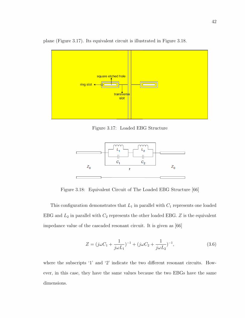
3.3.3 Loaded EBG in the Ground Plane (Electromagnetic
Band-gaps)
Electromagnetic band-gaps have caught recent attention in the microwave and millimeter-
wave community because of their filtering properties or inhibition of signal propaga-
tion in certain directions [66]. These EBG structures can be etched in the ground
42
plane (Figure 3.17). Its equivalent circuit is illustrated in Figure 3.18.
Figure 3.17: Loaded EBG Structure
Figure 3.18: Equivalent Circuit of The Loaded EBG Structure [66]
This configuration demonstrates that L1 in parallel with C1 represents one loaded
EBG and L2 in parallel with C2 represents the other loaded EBG. Z is the equivalent
impedance value of the cascaded resonant circuit. It is given as [66]
Z = (jωC1 +1
jωL1
)−1 + (jωC2 +1
jωL2
)−1, (3.6)
where the subscripts ‘1’ and ‘2’ indicate the two different resonant circuits. How-
ever, in this case, they have the same values because the two EBGs have the same
dimensions.
43
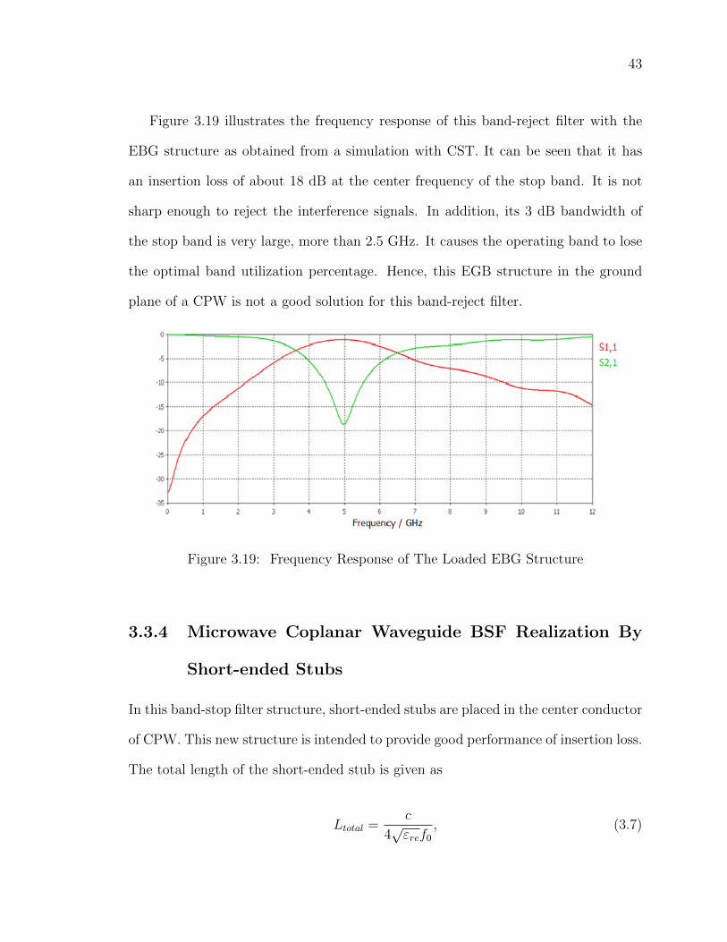
Figure 3.19 illustrates the frequency response of this band-reject filter with the
EBG structure as obtained from a simulation with CST. It can be seen that it has
an insertion loss of about 18 dB at the center frequency of the stop band. It is not
sharp enough to reject the interference signals. In addition, its 3 dB bandwidth of
the stop band is very large, more than 2.5 GHz. It causes the operating band to lose
the optimal band utilization percentage. Hence, this EGB structure in the ground
plane of a CPW is not a good solution for this band-reject filter.
Figure 3.19: Frequency Response of The Loaded EBG Structure
3.3.4 Microwave Coplanar Waveguide BSF Realization By
Short-ended Stubs
In this band-stop filter structure, short-ended stubs are placed in the center conductor
of CPW. This new structure is intended to provide good performance of insertion loss.
The total length of the short-ended stub is given as
Ltotal =c
4√εref0
, (3.7)
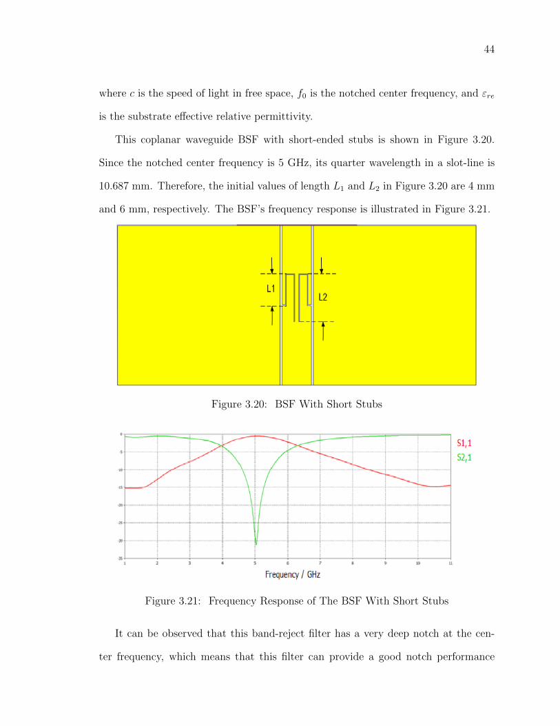
44
where c is the speed of light in free space, f0 is the notched center frequency, and εre
is the substrate effective relative permittivity.
This coplanar waveguide BSF with short-ended stubs is shown in Figure 3.20.
Since the notched center frequency is 5 GHz, its quarter wavelength in a slot-line is
10.687 mm. Therefore, the initial values of length L1 and L2 in Figure 3.20 are 4 mm
and 6 mm, respectively. The BSF’s frequency response is illustrated in Figure 3.21.
Figure 3.20: BSF With Short Stubs
Figure 3.21: Frequency Response of The BSF With Short Stubs
It can be observed that this band-reject filter has a very deep notch at the cen-
ter frequency, which means that this filter can provide a good notch performance
45
around 5 GHz. However, its 3 dB bandwidth is too wide to make an efficient band
usage. Therefore, this structure is not practical to be exploited in the UWB antenna
application.
3.3.5 CPW Band-stop Filter with Periodically Loaded Slot
Resonators
In this section, a new dual-spiral-shaped slot resonator in a co-planar waveguide
(CPW-DSR) is presented and its model is established in CST. This CPW-DSR is
placed in the ground plane as a band-stop filter as shown in Figure 3.22.
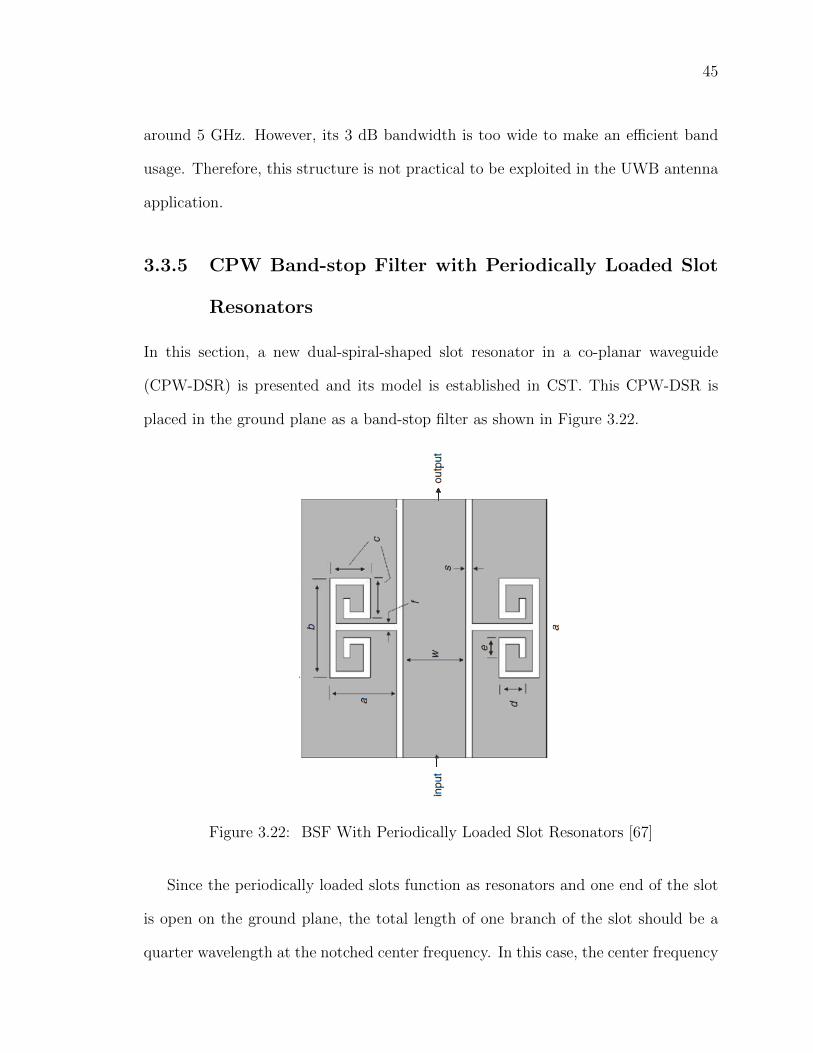
Figure 3.22: BSF With Periodically Loaded Slot Resonators [67]
Since the periodically loaded slots function as resonators and one end of the slot
is open on the ground plane, the total length of one branch of the slot should be a
quarter wavelength at the notched center frequency. In this case, the center frequency
46
is 5 GHz, so the quarter wavelength for the slot-line is about 10mm. Thus the initial
values for a, b, c, d, e and f are 3.2 mm, 6 mm, 2.4 mm, 1 mm, 0.6 mm and 0.2 mm,
respectively.
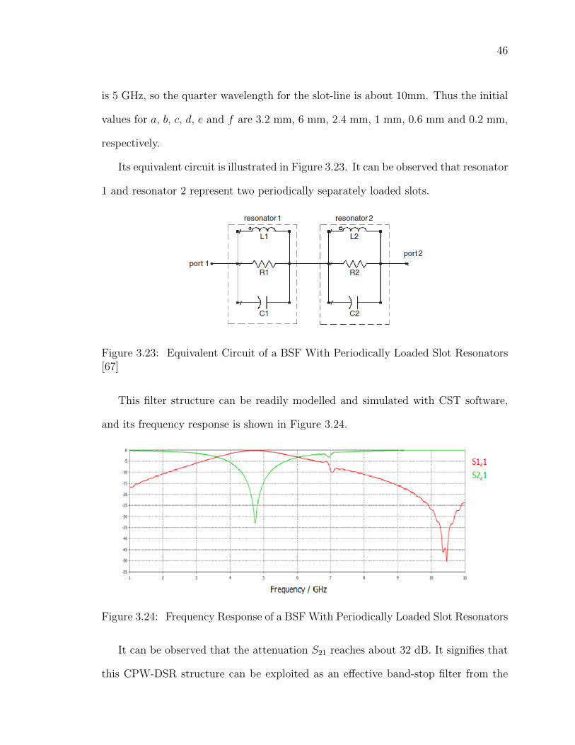
Its equivalent circuit is illustrated in Figure 3.23. It can be observed that resonator
1 and resonator 2 represent two periodically separately loaded slots.
Figure 3.23: Equivalent Circuit of a BSF With Periodically Loaded Slot Resonators[67]
This filter structure can be readily modelled and simulated with CST software,
and its frequency response is shown in Figure 3.24.
Figure 3.24: Frequency Response of a BSF With Periodically Loaded Slot Resonators
It can be observed that the attenuation S21 reaches about 32 dB. It signifies that
this CPW-DSR structure can be exploited as an effective band-stop filter from the
47
insertion loss point of view. However, its 3 dB bandwidth is more than 2 GHz. Thus,
this structure is not practical for the UWB antenna application.
3.3.6 CPW Band-stop Filter With Defected Ground Struc-
ture (DGS)
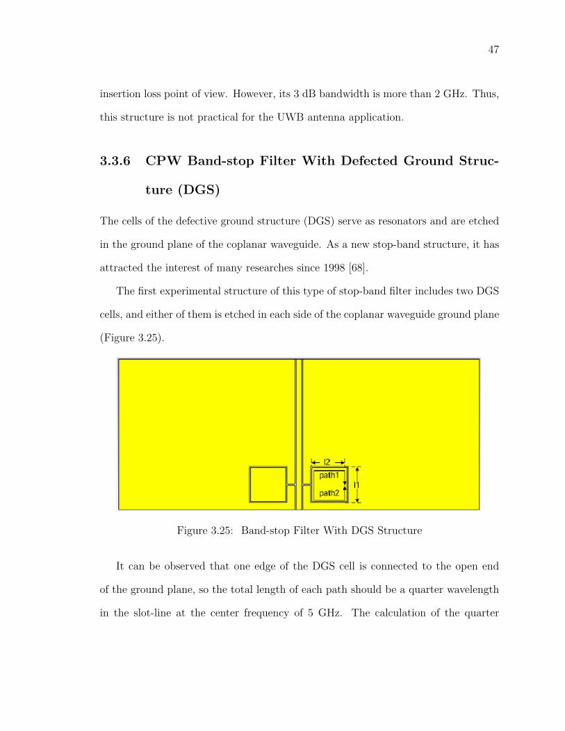
The cells of the defective ground structure (DGS) serve as resonators and are etched
in the ground plane of the coplanar waveguide. As a new stop-band structure, it has
attracted the interest of many researches since 1998 [68].
The first experimental structure of this type of stop-band filter includes two DGS
cells, and either of them is etched in each side of the coplanar waveguide ground plane
(Figure 3.25).
Figure 3.25: Band-stop Filter With DGS Structure
It can be observed that one edge of the DGS cell is connected to the open end
of the ground plane, so the total length of each path should be a quarter wavelength
in the slot-line at the center frequency of 5 GHz. The calculation of the quarter
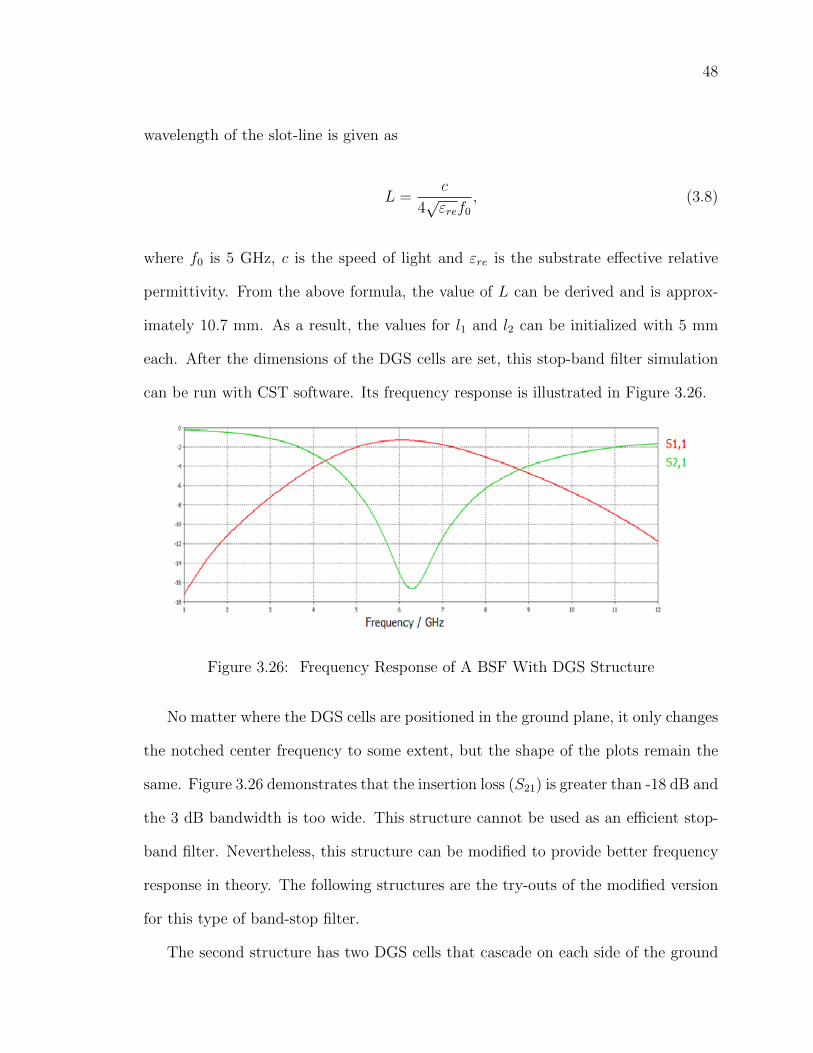
48
wavelength of the slot-line is given as
L =c
4√εref0
, (3.8)
where f0 is 5 GHz, c is the speed of light and εre is the substrate effective relative
permittivity. From the above formula, the value of L can be derived and is approx-
imately 10.7 mm. As a result, the values for l1 and l2 can be initialized with 5 mm
each. After the dimensions of the DGS cells are set, this stop-band filter simulation
can be run with CST software. Its frequency response is illustrated in Figure 3.26.
Figure 3.26: Frequency Response of A BSF With DGS Structure
No matter where the DGS cells are positioned in the ground plane, it only changes
the notched center frequency to some extent, but the shape of the plots remain the
same. Figure 3.26 demonstrates that the insertion loss (S21) is greater than -18 dB and
the 3 dB bandwidth is too wide. This structure cannot be used as an efficient stop-
band filter. Nevertheless, this structure can be modified to provide better frequency
response in theory. The following structures are the try-outs of the modified version
for this type of band-stop filter.
The second structure has two DGS cells that cascade on each side of the ground
49
plane (Figure 3.27). The distance between two DGS cells in each side of the ground
plane is around 0.155 mm. This is the minimum width that can be constructed by
the local fabricator. The idea of having two DGS cells on one side of the ground plane
is that the electromagnetic field is able to be coupled from the first DGS cell to the
second one. This should provide higher insertion loss in the stop band. Its frequency
response is shown in Figure 3.28.
Figure 3.27: Band-stop Filter With DGS Coupling Structure
Figure 3.28: Frequency Response of a BSF With DGS Coupling Structure
It can be observed that the frequency response of this structure does not differ
much from the previous structure. This can be attributed to the distance between
50
the two DGS cells in one side of the ground plane. It is too wide to yield a good
coupling between two DGS cells but it is the most narrow width able to be provided
by the manufacturer. Even though this structure is not suitable for a stop-band filter,
it leads to another similarly shaped structure.
The new structure is not intended to create coupling between two DGS cells but
to establish a path between two DGS cells (Figure 3.29). Initial values for l1 and l2
are given as 1 mm and 4 mm. Then the simulation of the above structure is run to
obtain the frequency response of this stop-band filter (Figure 3.30).
Figure 3.29: Band-stop Filter With DGS Through Structure
Figure 3.30: Frequency Response of A BSF With DGS Through Structure
51
It can be observed that there are two notches in the plot, and the second notch
will reach as low as -28 dB. This provides an acceptable insertion loss as a sharp
stop-band filter, but the 3 dB bandwidth is still too wide. l1 and l2 can be adjusted
to attempt to narrow down the 3 dB bandwidth. However, doing this only causes the
notched center point to move to the left or the right. Thus, this DGS cell structure
in the ground plane is not suitable for a band-stop filter in this case.
3.3.7 Substrate-Integrated Waveguide (SIW) Resonator Struc-
ture
Substrate-Integrated Waveguide (SIW) has attracted the millimeter-wave researchers’
attention since it is a reasonable compromise between planar integrated circuits and
metallic waveguide technology [69]. According to Table 3.1, the Q factors of CPW
and microstrip technologies are an order of magnitude lower than those of SIW. For
the purpose of this work, though, it is expected that SIW will provide narrower 3 dB
bandwidth and better attenuation in the stopband. Interfacing SIW with CPW is
becoming more and more popular in millimeter-wave applications. Figure 3.31 shows
the main SIW parameters. The transition between SIW and CPW is the key factor
to get a good frequency response for many applications.
CPW/Microstrip Integrated waveguide (SIW)Parameters h = 10 mil, εr = 2.33 h = 10 mil, εr = 2.33
Unloaded Q Factor 42 462
Table 3.1: Q Factor Comparison Between CPW/Microstrip and SIW
aequ is the equivalent waveguide width and is determined by the SIW’s cutoff
52
Figure 3.31: SIW Parameters [69]
frequency. It is given as
aequ =c
2fc√εr, (3.9)
where fc is the cut-off frequency and set to 4 GHz, c is the speed of light and εr is the
substrate relative permittivity. After aequ is obtained, the calculation of a is derived
by [70]
aequ = a[x1 +x2
pd
+ x1+x2−x3x3−x1
], (3.10a)
x1 = 1.0198 +0.3465
(ap− 1.0684)
, (3.10b)
x2 = −0.1183− 1.2729
(ap− 1.2010)
, (3.10c)
x3 = 1.0082− 0.9163
(ap
+ 0.2152), (3.10d)
where p is the distance between two via-hole centers, and d is the diameter of one
via-hole. The confinement for p and d is that d/p needs to be in range between 0.4
and 0.8 [71]. The best performance is when d/p > 0.5. In this case, the initial values
for p and d are 1.4 mm and 1 mm, respectively. The value of a is 22.626 mm from
the above formulas.
53
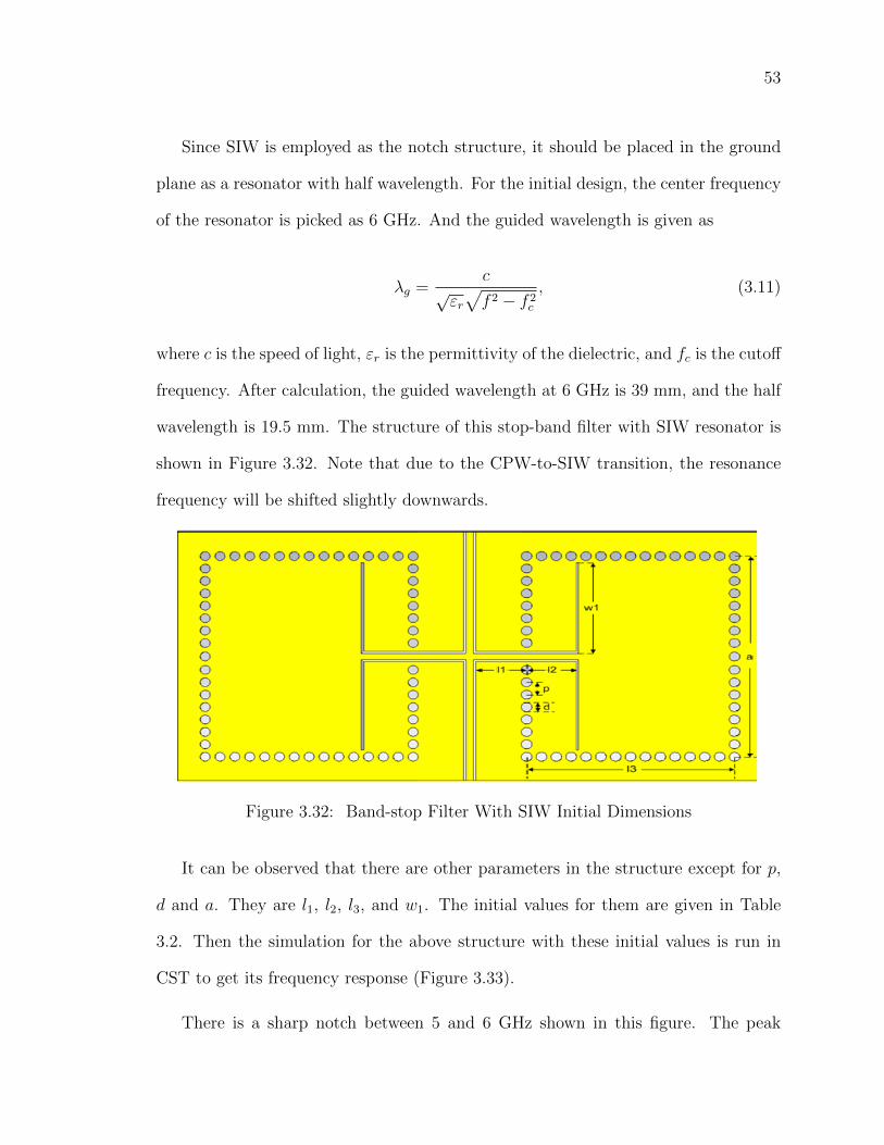
Since SIW is employed as the notch structure, it should be placed in the ground
plane as a resonator with half wavelength. For the initial design, the center frequency
of the resonator is picked as 6 GHz. And the guided wavelength is given as
λg =c
√εr√f 2 − f 2
c
, (3.11)
where c is the speed of light, εr is the permittivity of the dielectric, and fc is the cutoff
frequency. After calculation, the guided wavelength at 6 GHz is 39 mm, and the half
wavelength is 19.5 mm. The structure of this stop-band filter with SIW resonator is
shown in Figure 3.32. Note that due to the CPW-to-SIW transition, the resonance
frequency will be shifted slightly downwards.
Figure 3.32: Band-stop Filter With SIW Initial Dimensions
It can be observed that there are other parameters in the structure except for p,
d and a. They are l1, l2, l3, and w1. The initial values for them are given in Table
3.2. Then the simulation for the above structure with these initial values is run in
CST to get its frequency response (Figure 3.33).
There is a sharp notch between 5 and 6 GHz shown in this figure. The peak
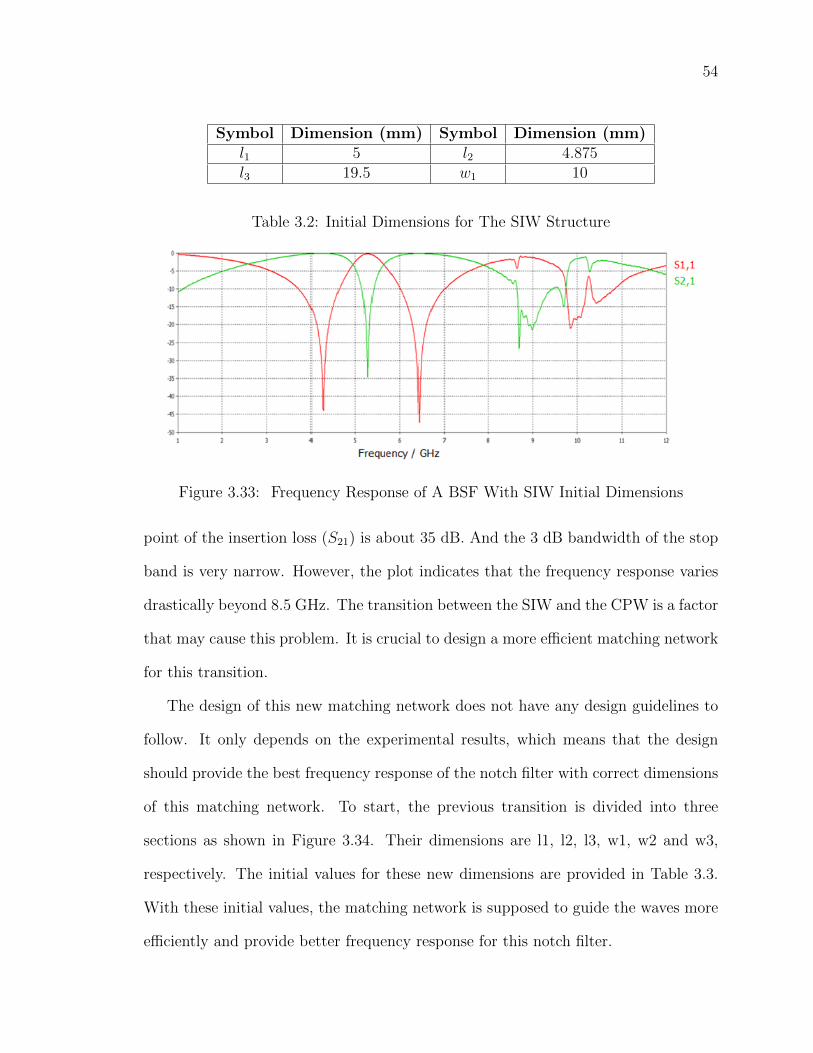
54
Symbol Dimension (mm) Symbol Dimension (mm)l1 5 l2 4.875l3 19.5 w1 10
Table 3.2: Initial Dimensions for The SIW Structure
Figure 3.33: Frequency Response of A BSF With SIW Initial Dimensions
point of the insertion loss (S21) is about 35 dB. And the 3 dB bandwidth of the stop
band is very narrow. However, the plot indicates that the frequency response varies
drastically beyond 8.5 GHz. The transition between the SIW and the CPW is a factor
that may cause this problem. It is crucial to design a more efficient matching network
for this transition.
The design of this new matching network does not have any design guidelines to
follow. It only depends on the experimental results, which means that the design
should provide the best frequency response of the notch filter with correct dimensions
of this matching network. To start, the previous transition is divided into three
sections as shown in Figure 3.34. Their dimensions are l1, l2, l3, w1, w2 and w3,
respectively. The initial values for these new dimensions are provided in Table 3.3.
With these initial values, the matching network is supposed to guide the waves more
efficiently and provide better frequency response for this notch filter.
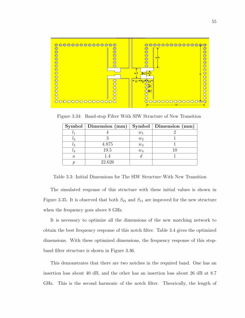
55
Figure 3.34: Band-stop Filter With SIW Structure of New Transition
Symbol Dimension (mm) Symbol Dimension (mm)l1 4 w1 2l2 3 w2 1l3 4.875 w3 1l4 19.5 w4 10a 1.4 d 1p 22.626
Table 3.3: Initial Dimensions for The SIW Structure With New Transition
The simulated response of this structure with these initial values is shown in
Figure 3.35. It is observed that both S21 and S11 are improved for the new structure
when the frequency goes above 8 GHz.
It is necessary to optimize all the dimensions of the new matching network to
obtain the best frequency response of this notch filter. Table 3.4 gives the optimized
dimensions. With these optimized dimensions, the frequency response of this stop-
band filter structure is shown in Figure 3.36.
This demonstrates that there are two notches in the required band. One has an
insertion loss about 40 dB, and the other has an insertion loss about 26 dB at 8.7
GHz. This is the second harmonic of the notch filter. Theorically, the length of
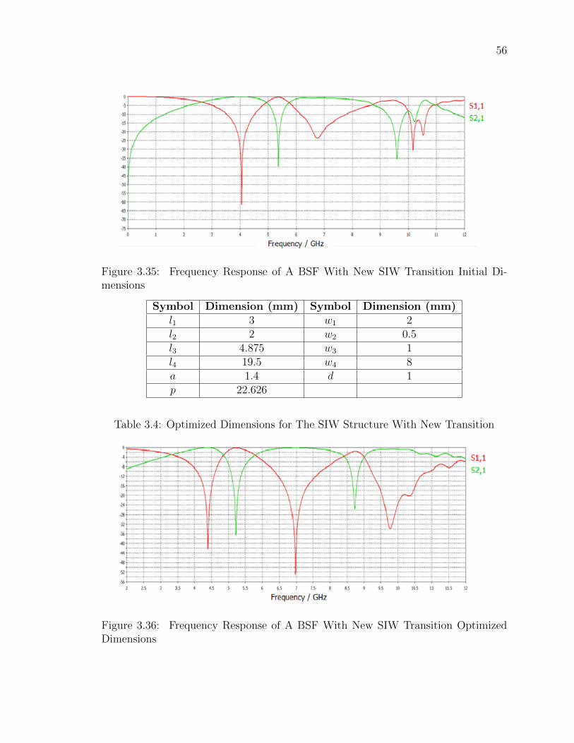
56
Figure 3.35: Frequency Response of A BSF With New SIW Transition Initial Di-mensions
Symbol Dimension (mm) Symbol Dimension (mm)l1 3 w1 2l2 2 w2 0.5l3 4.875 w3 1l4 19.5 w4 8a 1.4 d 1p 22.626
Table 3.4: Optimized Dimensions for The SIW Structure With New Transition
Figure 3.36: Frequency Response of A BSF With New SIW Transition OptimizedDimensions
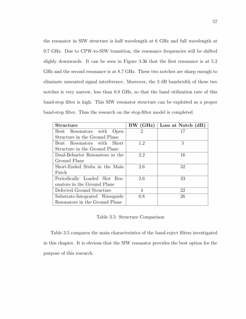
57
the resonator in SIW structure is half wavelength at 6 GHz and full wavelength at
9.7 GHz. Due to CPW-to-SIW transition, the resonance frequencies will be shifted
slighly downwards. It can be seen in Figure 3.36 that the first resonance is at 5.2
GHz and the second resonance is at 8.7 GHz. These two notches are sharp enough to
eliminate unwanted signal interference. Moreover, the 3 dB bandwidth of these two
notches is very narrow, less than 0.8 GHz, so that the band utilization rate of this
band-stop filter is high. This SIW resonator structure can be exploited as a proper
band-stop filter. Thus the research on the stop-filter model is completed.
Structure BW (GHz) Loss at Notch (dB)Bent Resonators with OpenStructure in the Ground Plane
2 17
Bent Resonators with ShortStructure in the Ground Plane
1.2 5
Dual-Beharior Resonators in theGround Plane
2.2 16
Short-Ended Stubs in the MainPatch
2.6 32
Periodically Loaded Slot Res-onators in the Ground Plane
2.6 33
Defected Ground Structure 4 22Substrate-Integrated WaveguideResonators in the Ground Plane
0.8 26
Table 3.5: Structure Comparison
Table 3.5 compares the main characteristics of the band-reject filters investigated
in this chapter. It is obvious that the SIW resonator provides the best option for the
purpose of this research.
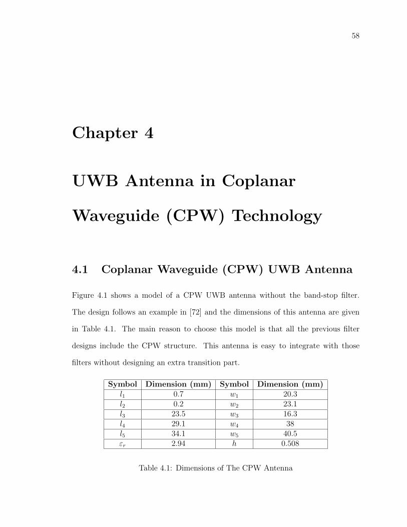
58
Chapter 4
UWB Antenna in Coplanar
Waveguide (CPW) Technology
4.1 Coplanar Waveguide (CPW) UWB Antenna
Figure 4.1 shows a model of a CPW UWB antenna without the band-stop filter.
The design follows an example in [72] and the dimensions of this antenna are given
in Table 4.1. The main reason to choose this model is that all the previous filter
designs include the CPW structure. This antenna is easy to integrate with those
filters without designing an extra transition part.
Symbol Dimension (mm) Symbol Dimension (mm)l1 0.7 w1 20.3l2 0.2 w2 23.1l3 23.5 w3 16.3l4 29.1 w4 38l5 34.1 w5 40.5εr 2.94 h 0.508
Table 4.1: Dimensions of The CPW Antenna
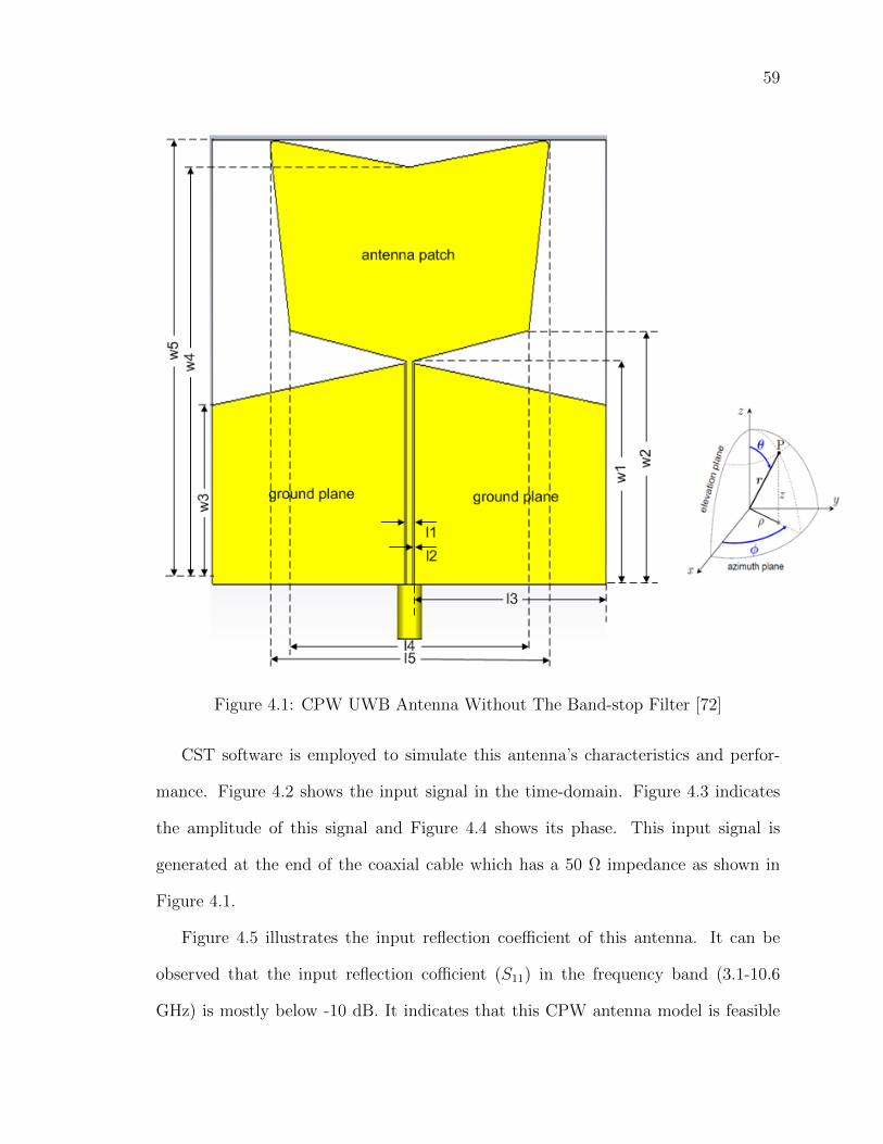
59
Figure 4.1: CPW UWB Antenna Without The Band-stop Filter [72]
CST software is employed to simulate this antenna’s characteristics and perfor-
mance. Figure 4.2 shows the input signal in the time-domain. Figure 4.3 indicates
the amplitude of this signal and Figure 4.4 shows its phase. This input signal is
generated at the end of the coaxial cable which has a 50 Ω impedance as shown in
Figure 4.1.
Figure 4.5 illustrates the input reflection coefficient of this antenna. It can be
observed that the input reflection cofficient (S11) in the frequency band (3.1-10.6
GHz) is mostly below -10 dB. It indicates that this CPW antenna model is feasible
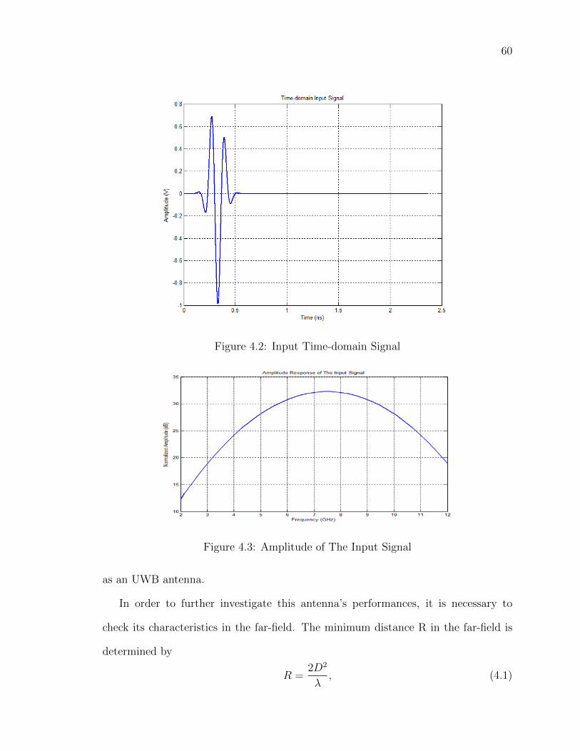
60
Figure 4.2: Input Time-domain Signal
Figure 4.3: Amplitude of The Input Signal
as an UWB antenna.
In order to further investigate this antenna’s performances, it is necessary to
check its characteristics in the far-field. The minimum distance R in the far-field is
determined by
R =2D2
λ, (4.1)
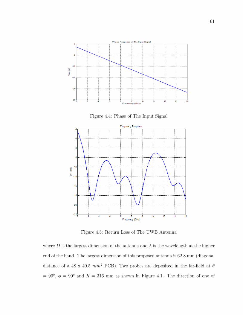
61
Figure 4.4: Phase of The Input Signal
Figure 4.5: Return Loss of The UWB Antenna
where D is the largest dimension of the antenna and λ is the wavelength at the higher
end of the band. The largest dimension of this proposed antenna is 62.8 mm (diagonal
distance of a 48 x 40.5 mm2 PCB). Two probes are deposited in the far-field at θ
= 90o, φ = 90o and R = 316 mm as shown in Figure 4.1. The direction of one of
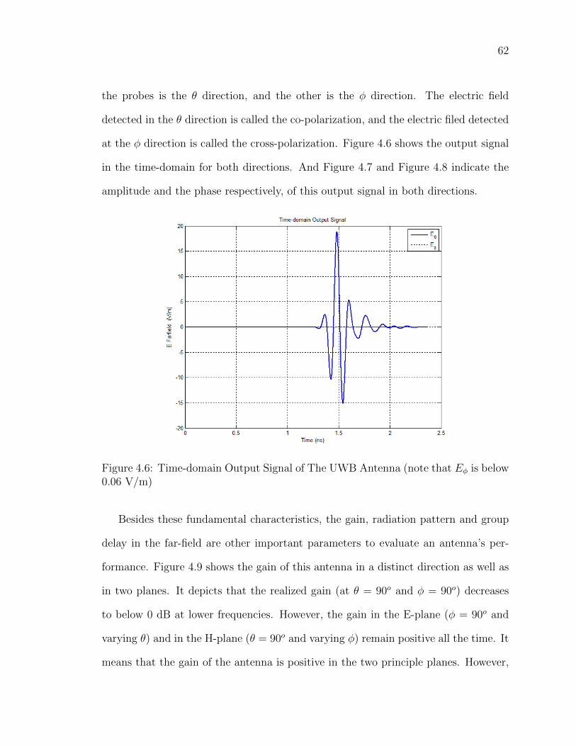
62
the probes is the θ direction, and the other is the φ direction. The electric field
detected in the θ direction is called the co-polarization, and the electric filed detected
at the φ direction is called the cross-polarization. Figure 4.6 shows the output signal
in the time-domain for both directions. And Figure 4.7 and Figure 4.8 indicate the
amplitude and the phase respectively, of this output signal in both directions.
Figure 4.6: Time-domain Output Signal of The UWB Antenna (note that Eφ is below0.06 V/m)
Besides these fundamental characteristics, the gain, radiation pattern and group
delay in the far-field are other important parameters to evaluate an antenna’s per-
formance. Figure 4.9 shows the gain of this antenna in a distinct direction as well as
in two planes. It depicts that the realized gain (at θ = 90o and φ = 90o) decreases
to below 0 dB at lower frequencies. However, the gain in the E-plane (φ = 90o and
varying θ) and in the H-plane (θ = 90o and varying φ) remain positive all the time. It
means that the gain of the antenna is positive in the two principle planes. However,
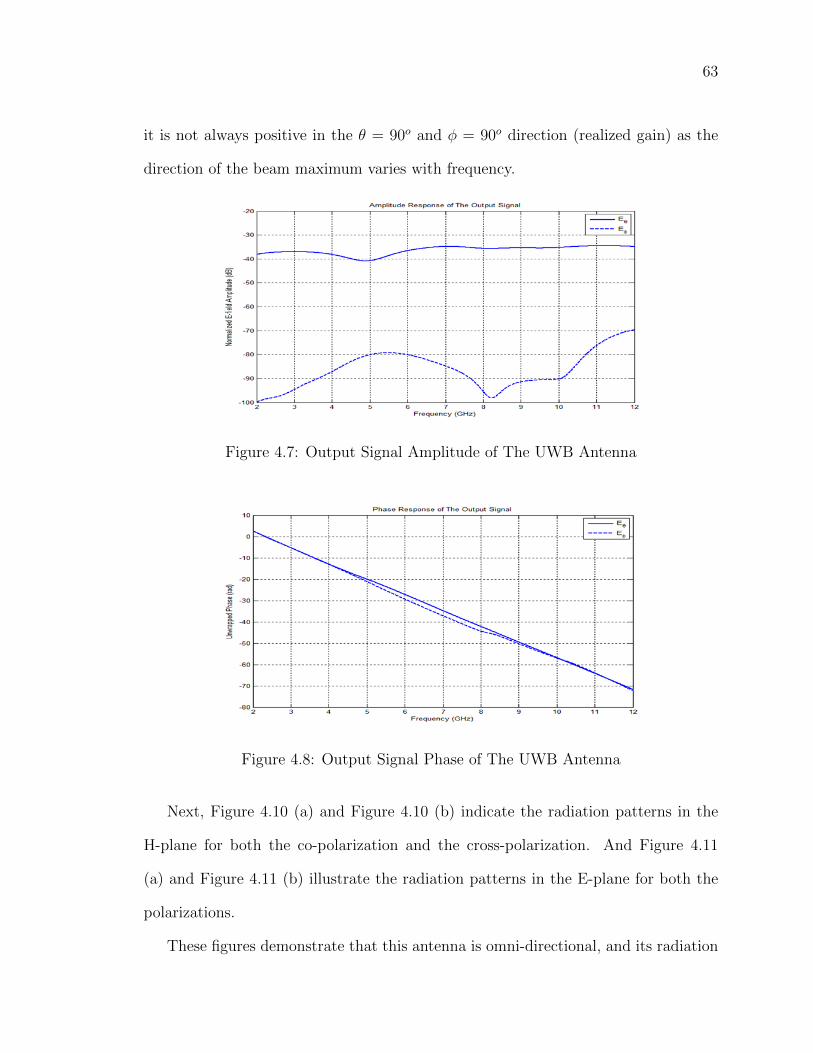
63
it is not always positive in the θ = 90o and φ = 90o direction (realized gain) as the
direction of the beam maximum varies with frequency.
Figure 4.7: Output Signal Amplitude of The UWB Antenna
Figure 4.8: Output Signal Phase of The UWB Antenna
Next, Figure 4.10 (a) and Figure 4.10 (b) indicate the radiation patterns in the
H-plane for both the co-polarization and the cross-polarization. And Figure 4.11
(a) and Figure 4.11 (b) illustrate the radiation patterns in the E-plane for both the
polarizations.
These figures demonstrate that this antenna is omni-directional, and its radiation
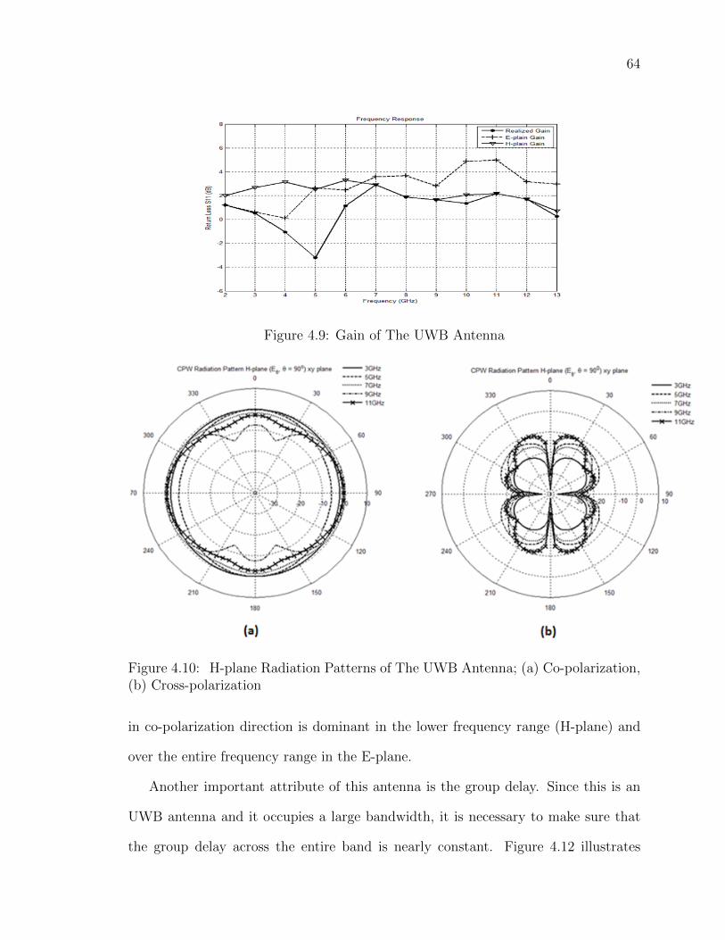
64
Figure 4.9: Gain of The UWB Antenna
Figure 4.10: H-plane Radiation Patterns of The UWB Antenna; (a) Co-polarization,(b) Cross-polarization
in co-polarization direction is dominant in the lower frequency range (H-plane) and
over the entire frequency range in the E-plane.
Another important attribute of this antenna is the group delay. Since this is an
UWB antenna and it occupies a large bandwidth, it is necessary to make sure that
the group delay across the entire band is nearly constant. Figure 4.12 illustrates
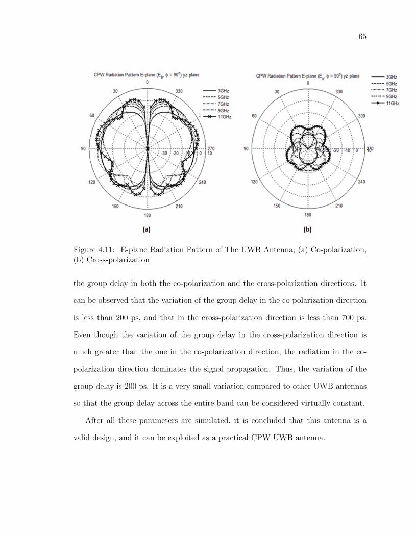
65
Figure 4.11: E-plane Radiation Pattern of The UWB Antenna; (a) Co-polarization,(b) Cross-polarization
the group delay in both the co-polarization and the cross-polarization directions. It
can be observed that the variation of the group delay in the co-polarization direction
is less than 200 ps, and that in the cross-polarization direction is less than 700 ps.
Even though the variation of the group delay in the cross-polarization direction is
much greater than the one in the co-polarization direction, the radiation in the co-
polarization direction dominates the signal propagation. Thus, the variation of the
group delay is 200 ps. It is a very small variation compared to other UWB antennas
so that the group delay across the entire band can be considered virtually constant.
After all these parameters are simulated, it is concluded that this antenna is a
valid design, and it can be exploited as a practical CPW UWB antenna.
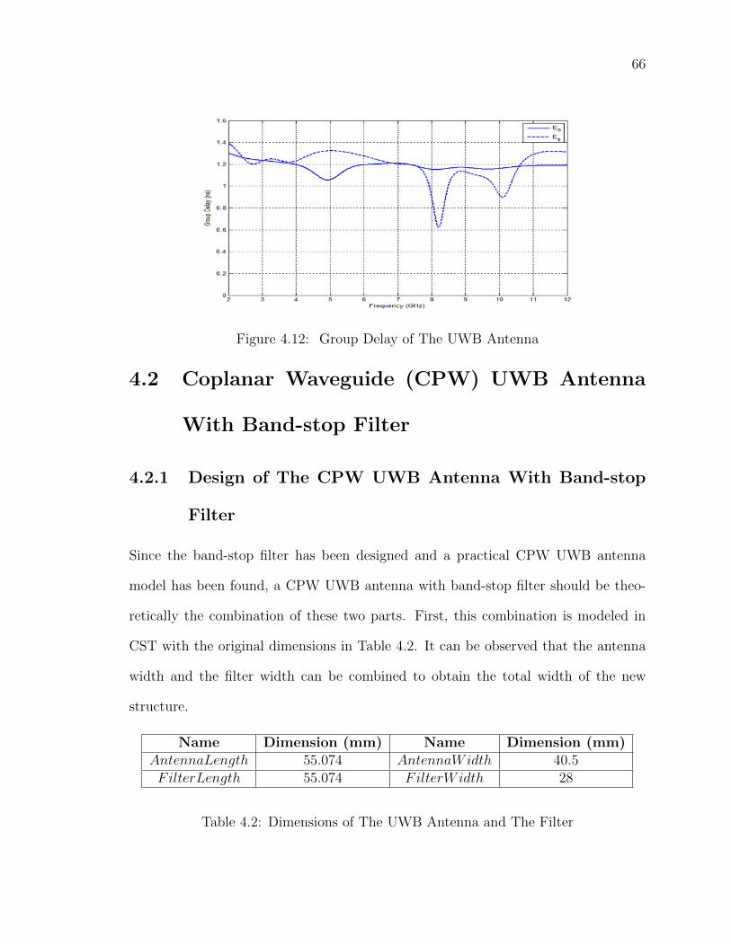
66
Figure 4.12: Group Delay of The UWB Antenna
4.2 Coplanar Waveguide (CPW) UWB Antenna
With Band-stop Filter
4.2.1 Design of The CPW UWB Antenna With Band-stop
Filter
Since the band-stop filter has been designed and a practical CPW UWB antenna
model has been found, a CPW UWB antenna with band-stop filter should be theo-
retically the combination of these two parts. First, this combination is modeled in
CST with the original dimensions in Table 4.2. It can be observed that the antenna
width and the filter width can be combined to obtain the total width of the new
structure.
Name Dimension (mm) Name Dimension (mm)AntennaLength 55.074 AntennaWidth 40.5FilterLength 55.074 FilterWidth 28
Table 4.2: Dimensions of The UWB Antenna and The Filter

67
Figure 4.13 shows this combined structure, and it is the initial design of the CPW
UWB antenna with the band-stop filter. The frequency response of this antenna is
shown in Figure 4.14.
Figure 4.13: CPW UWB Antenna With Stop-band Filter
The frequency response depicts that the entire band from 3.1-10.6 GHz has been
divided into three sub-bands. The first sub-band is from 4.1-4.6 GHz, the second
one is from 6.6-8.2 GHz, and the third one is from 9.3-10.8 GHz. It proves that this
CPW UWB antenna with stop-band filter performs according to theory. Next, it is
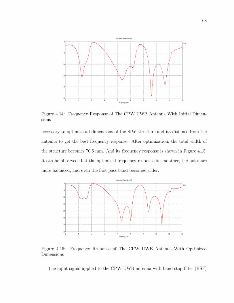
68
Figure 4.14: Frequency Response of The CPW UWB Antenna With Initial Dimen-sions
necessary to optimize all dimensions of the SIW structure and its distance from the
antenna to get the best frequency response. After optimization, the total width of
the structure becomes 70.5 mm. And its frequency response is shown in Figure 4.15.
It can be observed that the optimized frequency response is smoother, the poles are
more balanced, and even the first pass-band becomes wider.
Figure 4.15: Frequency Response of The CPW UWB Antenna With OptimizedDimensions
The input signal applied to the CPW UWB antenna with band-stop filter (BSF)
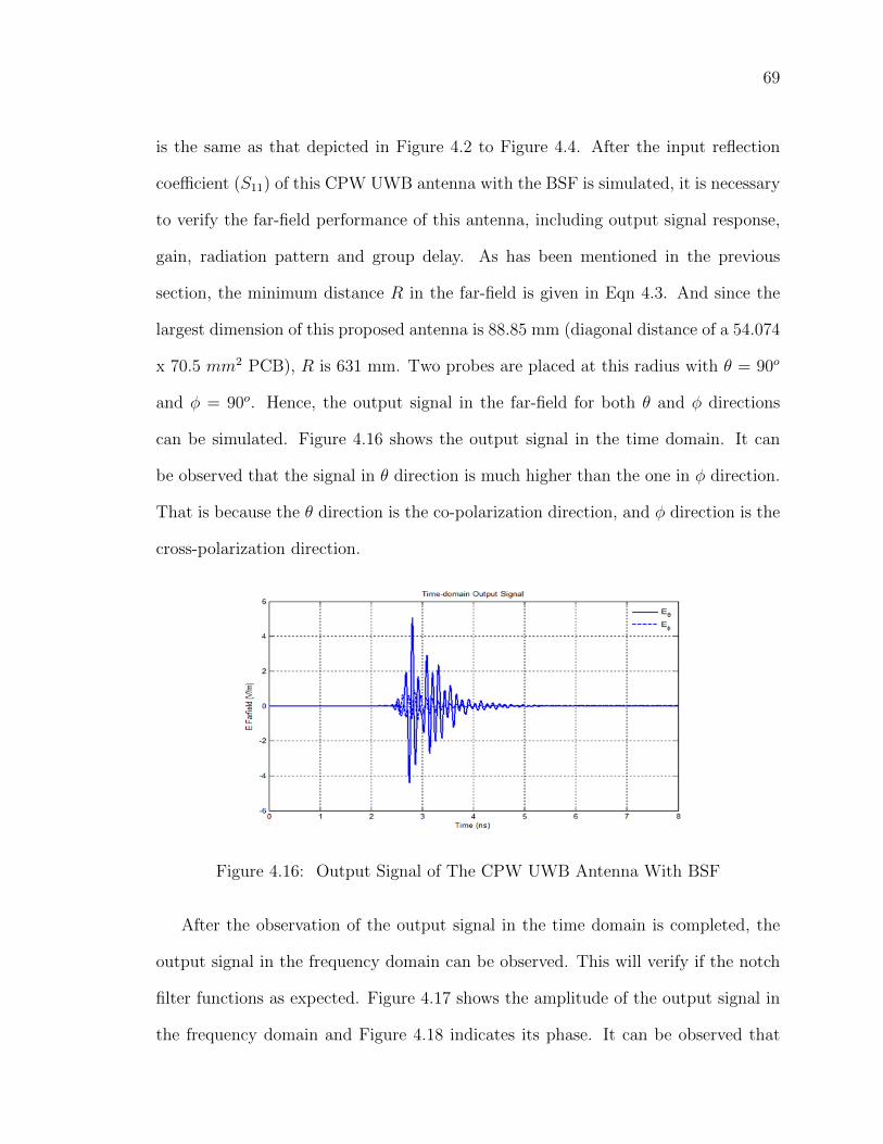
69
is the same as that depicted in Figure 4.2 to Figure 4.4. After the input reflection
coefficient (S11) of this CPW UWB antenna with the BSF is simulated, it is necessary
to verify the far-field performance of this antenna, including output signal response,
gain, radiation pattern and group delay. As has been mentioned in the previous
section, the minimum distance R in the far-field is given in Eqn 4.3. And since the
largest dimension of this proposed antenna is 88.85 mm (diagonal distance of a 54.074
x 70.5 mm2 PCB), R is 631 mm. Two probes are placed at this radius with θ = 90o
and φ = 90o. Hence, the output signal in the far-field for both θ and φ directions
can be simulated. Figure 4.16 shows the output signal in the time domain. It can
be observed that the signal in θ direction is much higher than the one in φ direction.
That is because the θ direction is the co-polarization direction, and φ direction is the
cross-polarization direction.
Figure 4.16: Output Signal of The CPW UWB Antenna With BSF
After the observation of the output signal in the time domain is completed, the
output signal in the frequency domain can be observed. This will verify if the notch
filter functions as expected. Figure 4.17 shows the amplitude of the output signal in
the frequency domain and Figure 4.18 indicates its phase. It can be observed that
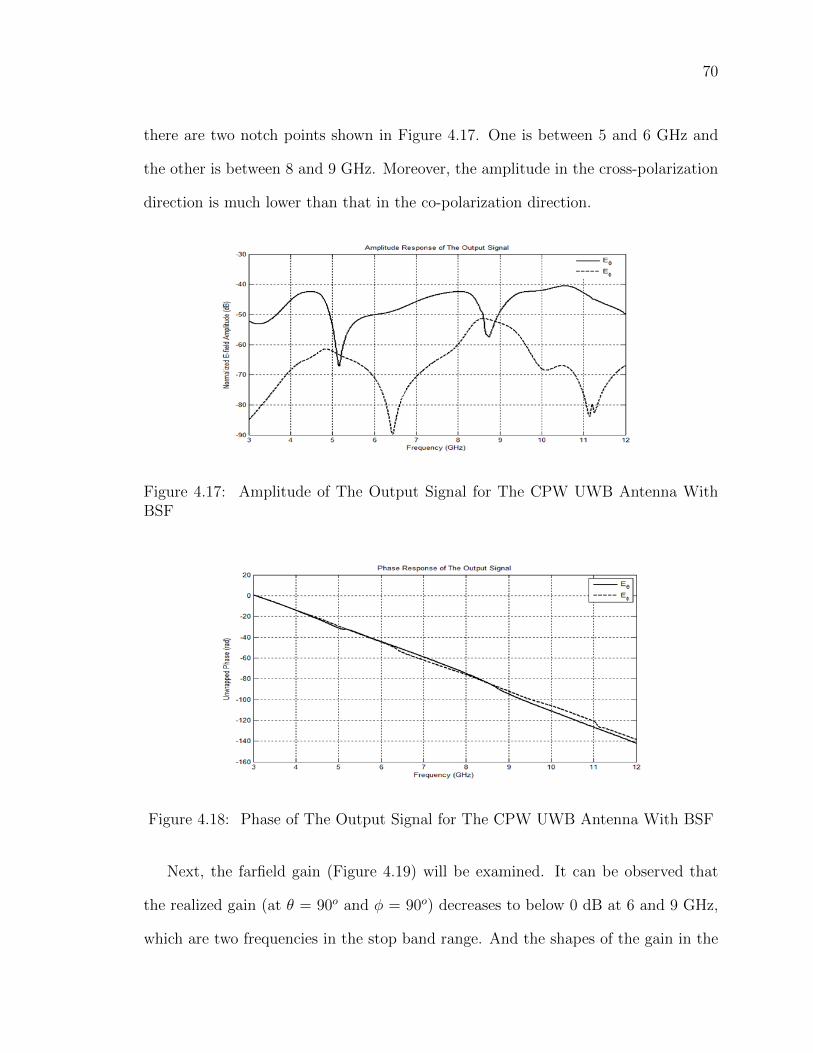
70
there are two notch points shown in Figure 4.17. One is between 5 and 6 GHz and
the other is between 8 and 9 GHz. Moreover, the amplitude in the cross-polarization
direction is much lower than that in the co-polarization direction.
Figure 4.17: Amplitude of The Output Signal for The CPW UWB Antenna WithBSF
Figure 4.18: Phase of The Output Signal for The CPW UWB Antenna With BSF
Next, the farfield gain (Figure 4.19) will be examined. It can be observed that
the realized gain (at θ = 90o and φ = 90o) decreases to below 0 dB at 6 and 9 GHz,
which are two frequencies in the stop band range. And the shapes of the gain in the

71
E-plane (φ = 90o and varying θ) and in the H-plane (θ = 90o and varying φ) agree
with that of the realized gain across frequencies. The only difference is that the first
notch point moves from 6 GHz to 5 GHz, but 5 GHz is still in the stop band range.
It verifies that the notch filter functions properly.
Figure 4.19: Gain of This CPW UWB Antenna
After that, the radiation patterns in both E-plane and H-plane need to be exam-
ined. Table 4.3 shows the frequencies to be simulated. The reason to choose these
frequencies is that they individually represent different pass bands and stop bands.
Name Frequency (GHz) Name Frequency (GHz)f1 4.3 f2 5f3 7 f4 9f5 10
Table 4.3: Simulated Frequencies
Figure 4.20 (a) and Figure 4.20 (b) indicate the radiation patterns in the H-
plane for both the co-polarization and the cross-polarization. And Figure 4.21 (a)
and Figure 4.21 (b) illustrate the radiation patterns in the E-plane for both the
polarizations. It can be observed that regardless of the principal plane (E-plane or H-
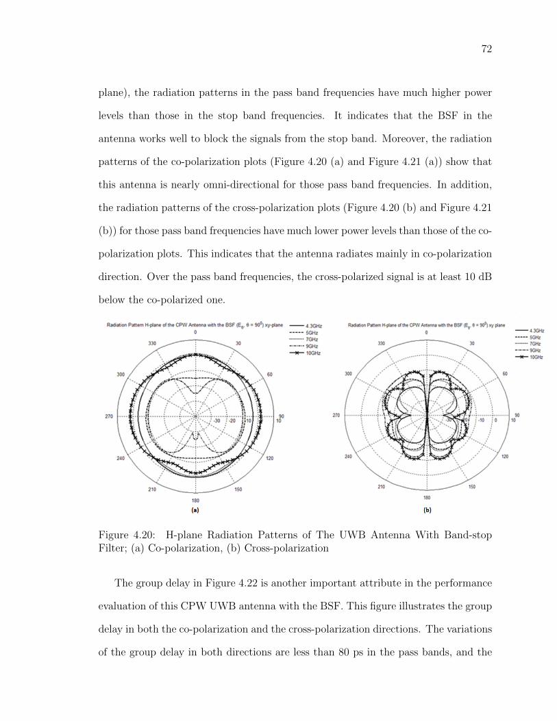
72
plane), the radiation patterns in the pass band frequencies have much higher power
levels than those in the stop band frequencies. It indicates that the BSF in the
antenna works well to block the signals from the stop band. Moreover, the radiation
patterns of the co-polarization plots (Figure 4.20 (a) and Figure 4.21 (a)) show that
this antenna is nearly omni-directional for those pass band frequencies. In addition,
the radiation patterns of the cross-polarization plots (Figure 4.20 (b) and Figure 4.21
(b)) for those pass band frequencies have much lower power levels than those of the co-
polarization plots. This indicates that the antenna radiates mainly in co-polarization
direction. Over the pass band frequencies, the cross-polarized signal is at least 10 dB
below the co-polarized one.
Figure 4.20: H-plane Radiation Patterns of The UWB Antenna With Band-stopFilter; (a) Co-polarization, (b) Cross-polarization
The group delay in Figure 4.22 is another important attribute in the performance
evaluation of this CPW UWB antenna with the BSF. This figure illustrates the group
delay in both the co-polarization and the cross-polarization directions. The variations
of the group delay in both directions are less than 80 ps in the pass bands, and the
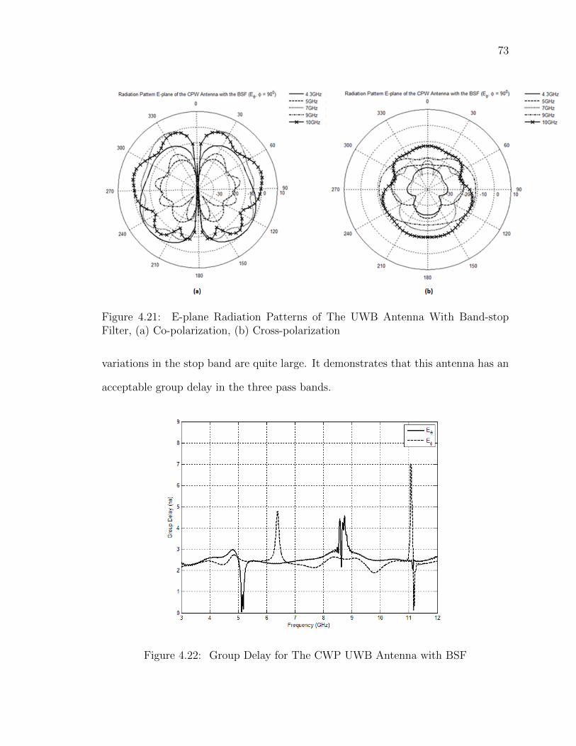
73
Figure 4.21: E-plane Radiation Patterns of The UWB Antenna With Band-stopFilter, (a) Co-polarization, (b) Cross-polarization
variations in the stop band are quite large. It demonstrates that this antenna has an
acceptable group delay in the three pass bands.
Figure 4.22: Group Delay for The CWP UWB Antenna with BSF
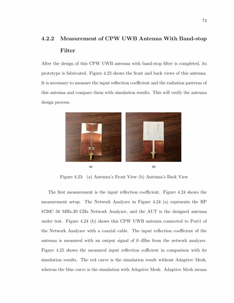
74
4.2.2 Measurement of CPW UWB Antenna With Band-stop
Filter
After the design of this CPW UWB antenna with band-stop filter is completed, its
prototype is fabricated. Figure 4.23 shows the front and back views of this antenna.
It is necessary to measure the input reflection coefficient and the radiation patterns of
this antenna and compare them with simulation results. This will verify the antenna
design process.
Figure 4.23: (a) Antenna’s Front View (b) Antenna’s Back View
The first measurement is the input reflection coefficient. Figure 4.24 shows the
measurement setup. The Network Analyzer in Figure 4.24 (a) represents the HP
8720C 50 MHz-20 GHz Network Analyzer, and the AUT is the designed antenna
under test. Figure 4.24 (b) shows this CPW UWB antenna connected to Port1 of
the Network Analyzer with a coaxial cable. The input reflection coefficient of the
antenna is measured with an output signal of 0 dBm from the network analyzer.
Figure 4.25 shows the measured input reflection cofficient in comparison with its
simulation results. The red curve is the simulation result without Adaptive Mesh,
whereas the blue curve is the simulation with Adaptive Mesh. Adaptive Mesh means
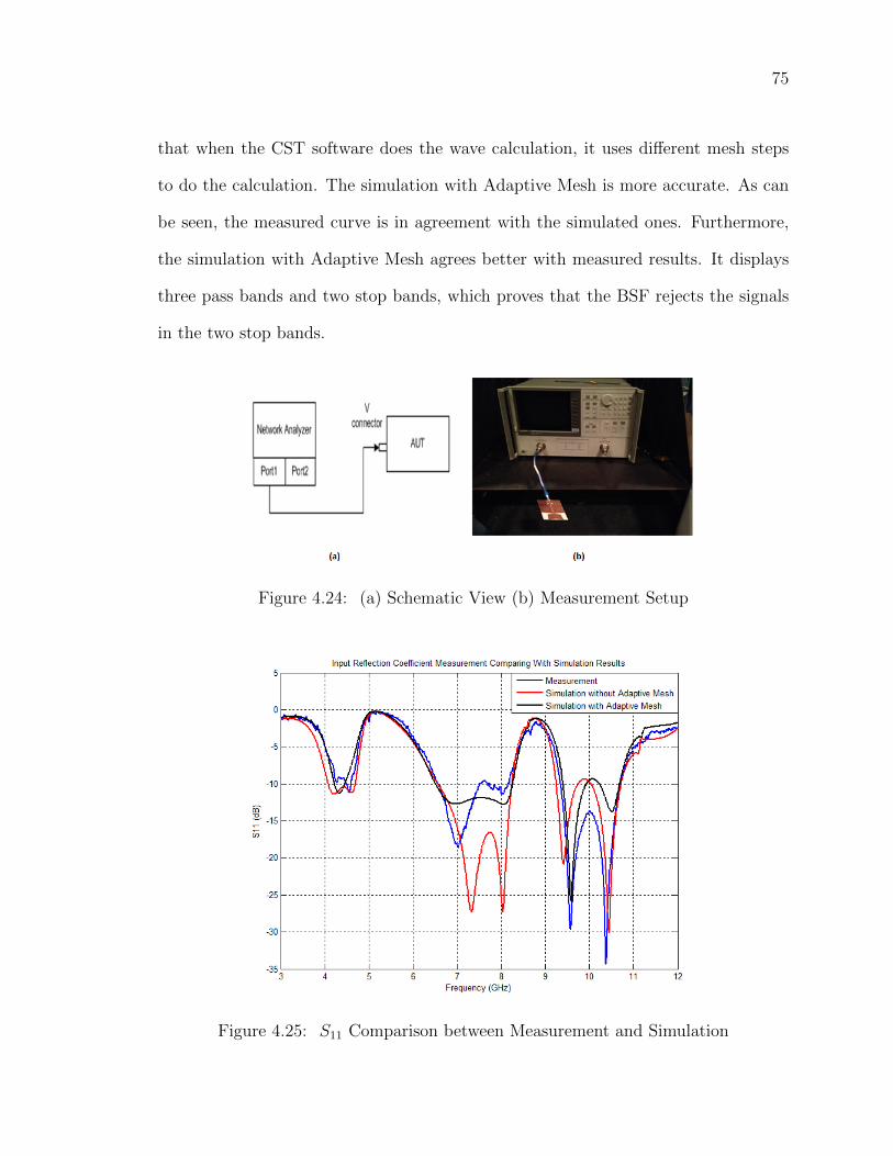
75
that when the CST software does the wave calculation, it uses different mesh steps
to do the calculation. The simulation with Adaptive Mesh is more accurate. As can
be seen, the measured curve is in agreement with the simulated ones. Furthermore,
the simulation with Adaptive Mesh agrees better with measured results. It displays
three pass bands and two stop bands, which proves that the BSF rejects the signals
in the two stop bands.
Figure 4.24: (a) Schematic View (b) Measurement Setup
Figure 4.25: S11 Comparison between Measurement and Simulation
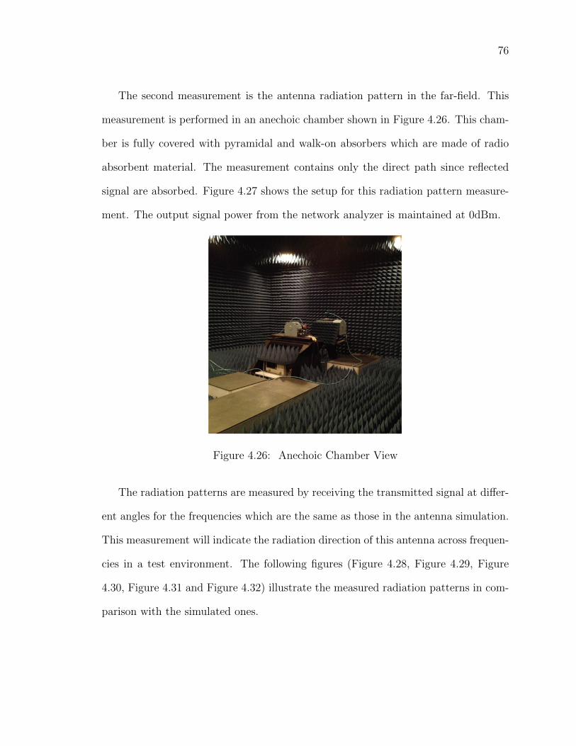
76
The second measurement is the antenna radiation pattern in the far-field. This
measurement is performed in an anechoic chamber shown in Figure 4.26. This cham-
ber is fully covered with pyramidal and walk-on absorbers which are made of radio
absorbent material. The measurement contains only the direct path since reflected
signal are absorbed. Figure 4.27 shows the setup for this radiation pattern measure-
ment. The output signal power from the network analyzer is maintained at 0dBm.
Figure 4.26: Anechoic Chamber View
The radiation patterns are measured by receiving the transmitted signal at differ-
ent angles for the frequencies which are the same as those in the antenna simulation.
This measurement will indicate the radiation direction of this antenna across frequen-
cies in a test environment. The following figures (Figure 4.28, Figure 4.29, Figure
4.30, Figure 4.31 and Figure 4.32) illustrate the measured radiation patterns in com-
parison with the simulated ones.
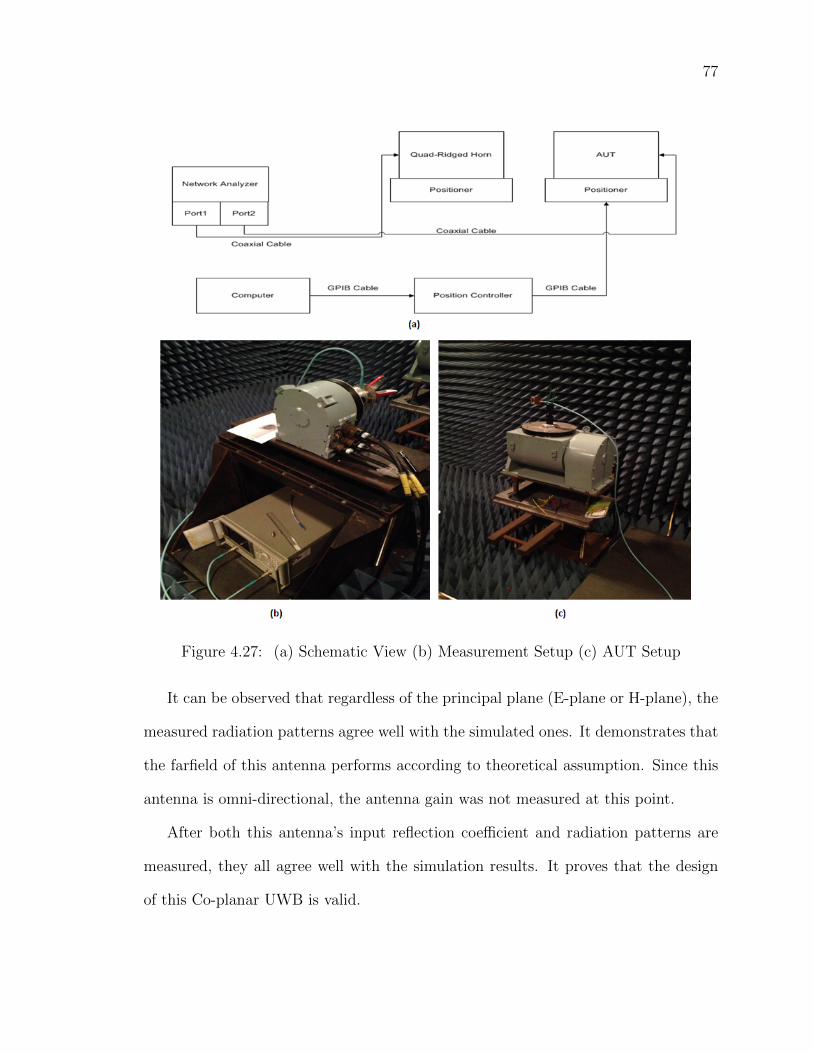
77
Figure 4.27: (a) Schematic View (b) Measurement Setup (c) AUT Setup
It can be observed that regardless of the principal plane (E-plane or H-plane), the
measured radiation patterns agree well with the simulated ones. It demonstrates that
the farfield of this antenna performs according to theoretical assumption. Since this
antenna is omni-directional, the antenna gain was not measured at this point.
After both this antenna’s input reflection coefficient and radiation patterns are
measured, they all agree well with the simulation results. It proves that the design
of this Co-planar UWB is valid.

78
Figure 4.28: H-plane and E-plane Radiation Patterns Measurement of The UWBAntenna With Band-stop Filter at 4.3GHz; (a) H-plane Co-polarization, (b) H-planeCross-polarization, (c) E-plane Co-polarization, (d) E-plane Cross-polarization
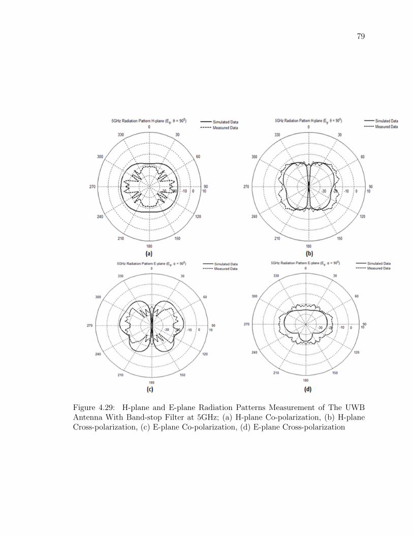
79
Figure 4.29: H-plane and E-plane Radiation Patterns Measurement of The UWBAntenna With Band-stop Filter at 5GHz; (a) H-plane Co-polarization, (b) H-planeCross-polarization, (c) E-plane Co-polarization, (d) E-plane Cross-polarization
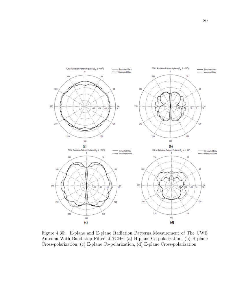
80
Figure 4.30: H-plane and E-plane Radiation Patterns Measurement of The UWBAntenna With Band-stop Filter at 7GHz; (a) H-plane Co-polarization, (b) H-planeCross-polarization, (c) E-plane Co-polarization, (d) E-plane Cross-polarization
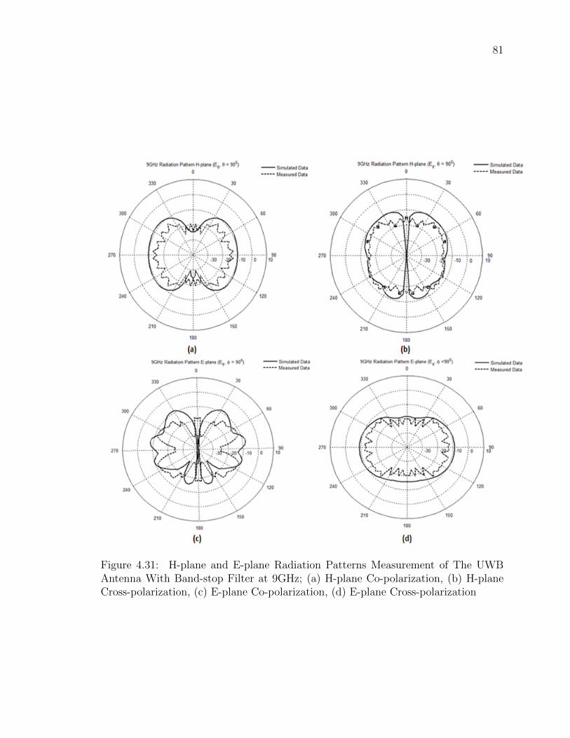
81
Figure 4.31: H-plane and E-plane Radiation Patterns Measurement of The UWBAntenna With Band-stop Filter at 9GHz; (a) H-plane Co-polarization, (b) H-planeCross-polarization, (c) E-plane Co-polarization, (d) E-plane Cross-polarization
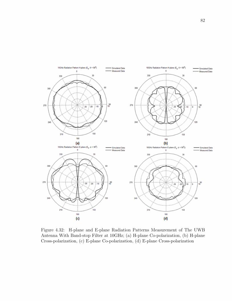
82
Figure 4.32: H-plane and E-plane Radiation Patterns Measurement of The UWBAntenna With Band-stop Filter at 10GHz; (a) H-plane Co-polarization, (b) H-planeCross-polarization, (c) E-plane Co-polarization, (d) E-plane Cross-polarization
83
Chapter 5
Conclusions
UWB technology presents a viable solution for future telecommunication, radar and
WPAN systems due to its extremely high data transmission rate. This high data
rate is attributed to the large frequency spectrum. Since the FCC released the 3.1-
10.6 GHz band for UWB communications, a large number of UWB applications have
been developed. However, the existing wireless networks such as IEEE 802.11a and
HIPERLAN/2 in Europe have occupied a band between 5 GHz and 6 GHz. It is
necessary to design a UWB antenna with a band-rejection filter to avoid this inter-
ference. The research of such a filter is carried out and the design of a UWB antenna
with this band-reject filter is achieved in this thesis.
Since there is a trend towards miniaturization of printed circuits, the development
of an UWB antenna with both microstrip technology and co-planar technology has
attracted more interest. Comparing with microstrip technology, co-planar technology
is easier to fabricate, has wider impedance match and better S parameters. The UWB
antenna with the band-reject filter in this thesis is prototyped in co-planar technology.
The research of this band-reject filter includes bent resonators in the ground plane,
84
DBRs in the ground plane, loaded EBGs in the ground plane, short-ended stubs in the
main patch, periodically loaded slot resonators in the ground plane, DGS structures,
and SIW structures. These circuits are modeled and simulated with CST Microwave
Studio. The frequency responses of the first six models have different defects so that
they are not practical enough to be exploited as a band-reject filter for this UWB
antenna. However, the SIW structure has provided highest insertion loss in the stop
band and the narrowest 3 dB bandwidth for the stop band. This SIW structure is
chosen as the band-reject filter.
After the research of the band-reject filter is completed, a UWB antenna in CPW
technology is modeled and simulated with CST Microwave Studio. According to this
antenna’s frequency response, gain, radiation pattern and group delay, it performs
well as a UWB antenna. Then, the final design is to combine this antenna with the
band-reject filter in order to separate the entire band into multiple sub-bands. Thus,
it can avoid interference from other existing wireless communications between 5 GHz
and 6 GHz. The final design is validated by its frequency response, gain, radiation
pattern and group delay. At this point, the design of this CPW UWB antenna with
the band-reject filter is accomplished. According to its tested performances, it can
be exploited as a practical UWB antenna.
85
Bibliography
[1] H.G. Schantz. A brief history of UWB antennas. IEEE Aerospace and Electronic
Systems Magazine, 19(4):22 – 26, April 2004.
[2] K. Kiminami, A. Hirata, and T. Shiozawa. Double-sided printed bow-tie antenna
for UWB communications. IEEE Antennas and Wireless Propagation Letters,
3(1):152 – 153, 2004.
[3] J. Liang, C.C. Chiau, X. Chen, and C.G. Parini. Printed circular disc monopole
antenna for ultra-wideband applications. IET Electronics Letters, 40(20):1246 –
1247, Sep. 2004.
[4] S.H. Choi, J.K. Park, S.K. Kim, and J.Y. Park. A new ultra-wideband antenna
for UWB applications. Microwave and Optical Technology Letters, 40(5):399 –
401, Mar. 2004.
[5] Jianxin Liang, C.C. Chiau, Xiaodong Chen, and C.G. Parini. Study of a printed
circular disc monopole antenna for UWB systems. IEEE Transactions on An-
tennas and Propagation, 53(11):3500 – 3504, Nov. 2005.
[6] Z.N. Low, J.H. Cheong, and C.L. Law. Low-cost PCB antenna for UWB appli-
cations. IEEE Antennas and Wireless Propagation Letters, 4:237 – 239, 2005.
86
[7] C.-C. Lin, Y.-C. Kan, L.-C. Kuo, and H.-R. Chuang. A planar triangular
monopole antenna for UWB communication. IEEE Microwave and Wireless
Components Letters, 15(10):624 – 626, 2005.
[8] H.R. Chuang, C.C. Lin, and Y.C. Kan. A printed UWB triangular monopole
antenna. Microwave Journal, 49:108 – 120, Jan. 2006.
[9] K. Rambabu, M.Z. Alam, and J. Bornemann. Design of compact dual-polarized
printed-circuit antenna for ultra-wideband applications. In 36th European Mi-
crowave Conference, Proceedings, pages 626 –629, Sep. 2006.
[10] D.-C. Chang, J.-C. Liu, and M.-Y. Liu. A novel tulip-shaped monopole antenna
for UWB applications. Microwave and Optical Technology Letters, 48(2):307 –
312, Feb. 2006.
[11] S.-F. Tseng and C.-L. Huang. Ultrawideband planar microstrip-fed monopole
antenna. Microwave and Optical Technology Letters, 49(1):183 – 185, Jan. 2007.
[12] J. Liang, C.C. Chiau, X. Chen, and C.G. Parini. CPW-fed circular ring monopole
antenna. In IEEE Antennas and Propagation Society International Symposium
Digest, volume 2A, pages 500 – 503, July. 2005.
[13] A.M. Abbosh, M.E. Bialkowski, M.V. Jacob, and J. Mazierska. Investigations
into an LTCC based ultra wideband antenna. In Asia-Pacific Microwave Con-
ference, Proceedings, volume 3, pages 1 – 4, Dec. 2005.
[14] C.T.H. Lim. A GCPW-fed printed antenna for UWB applications. In Asia-
Pacific Microwave Conference, Proceedings, volume 4, pages 1 – 3, Dec. 2005.
87
[15] X. Chen, J. Liang, P. Li, L. Guo, C.C. Chiau, and C.G. Parini. Planar UWB
monopole antennas. In Asia-Pacific Microwave Conference, Proceedings, vol-
ume 1, pages 1 – 4, Dec. 2005.
[16] H.K. Lee, J.K. Park, and J.N Lee. Design of a planar half-circle shaped UWB
notch antenna. Microwave and Optical Technology Letters, 47(1):9 – 11, Oct.
2005.
[17] Tzyh-Ghuang Ma and Chao-Hsiung Tseng. An ultrawideband coplanar
waveguide-fed tapered ring slot antenna. IEEE Transactions on Antennas and
Propagation, 54(4):1105 – 1110, Apr. 2006.
[18] Yi-Chieh Lee, Syuan-Ci Lin, and Jwo-Shiun Sun. CPW-fed UWB slot antenna.
In Asia-Pacific Microwave Conference, Proceedings, pages 1636 –1639, Dec. 2006.
[19] S. Nikolaou, D.E. Anagnostou, G.E. Ponchak, M.M. Tentzeris, and J. Papapoly-
merou. Compact ultra wide-band (UWB) CPW-fed elliptical monopole on liquid
crystal polymer (LCP). In IEEE Antennas and Propagation Society International
Symposium Digest, pages 4657 –4660, July. 2006.
[20] E.S. Angelopoulos, A.Z. Anastopoulos, C.E. Githonas, and D.I. Kaklamani. A
modified bow-tie slot antenna fed by a CPW-to-CPW transition loaded with
inductively coupled slots for ultra wide-band applications. In IEEE International
Workshop on Antenna Technology: Small Antennas and Novel Metamaterials,
IWAT 2005, pages 513 – 516, Mar. 2005.
[21] X.-L. Liang, S.-S. Zhong, and W. Wang. UWB printed circular monopole an-
tenna. Microwave and Optical Technology Letters, 48(8):1532 – 1534, Aug. 2006.
88
[22] J.-S. Sun, Y.-C. Lee, and S.-C. Lin. New design of a CPW-fed ultrawideband
slot antenna. Microwave and Optical Technology Letters, 49(3):561 – 564, Mar.
2007.
[23] D.-B. Lin, I.-T. Tang, and M.-Y. Tsou. A compact UWB antenna with CPW-
feed. Microwave and Optical Technology Letters, 49(3):564 – 567, Mar. 2007.
[24] R. Chair, A.A. Kishk, and K.F. Lee. Ultrawide-band coplanar waveguide-fed
rectangular slot antenna. IEEE Antennas and Wireless Propagation Letters,
3(1):227 –229, 2004.
[25] N. Fortino, G. Kossiavas, J.Y. Dauvignac, and R. Staraj. Novel antenna for ultra-
wideband communications. Microwave and Optical Technology Letters, 41(3):166
– 169, May. 2004.
[26] W. Wang, S.S. Zhong, and S.-B. Chen. A novel wideband coplanar-fed monopole
antenna. Microwave and Optical Technology Letters, 43(1):50 – 52, Oct. 2004.
[27] Joon Il Kim and Yong Jee. Design of ultrawideband coplanar waveguide-fed
LI-shape planar monopole antennas. IEEE Antennas and Wireless Propagation
Letters, 6:383 – 387, 2007.
[28] Zhi Ning Chen and Xianming Qing. Research and development of planar UWB
antennas. In Asia-Pacific Microwave Conference, Proceedings, volume 1, pages
1 – 4, Dec. 2005.
[29] B.L. Ooi, G. Zhao, M.S. Leong, K.M. Chua, and C.W.L. Albert. Wide-
band LTCC CPW-fed two-layered monopole antenna. IET Electronics Letters,
41(16):9 – 10, Aug. 2005.
89
[30] K. Rambabu, H.A. Thiart, J. Bornemann, and S.Y. Yu. Ultrawideband printed-
circuit antenna. IEEE Transactions on Antennas and Propagation, 54(12):3908
–3911, Dec. 2006.
[31] Z. Ying and J. Andersson. An ultra wideband ”cobra” patch antenna. IEE
Proceedings Microwaves, Antennas and Propagation, 151(6):486 – 490, Dec. 2004.
[32] H.M. Zamel, A.M. Attiya, and E.A. Hashish. Design of a compact UWB planar
antenna with band-notch characterization. In National Radio Science Confer-
ence, Proceedings, pages 1 – 8, Mar. 2007.
[33] Qing-Xin Chu and Ying-Ying Yang. A compact CPW-fed planar ultra-wideband
antenna with a frequency notch characteristic. In Asia-Pacific Microwave Con-
ference, Proceedings, pages 1 – 4, Dec. 2007.
[34] Se-Hwan Choi, Ho-Jun Lee, and Jong-Kyu Kim. Design of a ultra-wideband
antenna with band notch characteristic. In IEEE Antennas and Propagation
Society International Symposium Digest, pages 1 – 4, July. 2008.
[35] H.M. Jafari, M.J. Deen, S. Hranilovic, and N.K. Nikolova. Slot antenna for ultra-
wideband applications. In IEEE Antennas and Propagation Society International
Symposium Digest, pages 1107 – 1110, July. 2006.
[36] R.J. Fontana. A brief history of UWB communications. Transmission Microwave
Theory and Technology, 14(11):528 – 547, 1966.
[37] H.-J. Lam. Ultra-wideband antenna in coplanar technology. M.A.Sc. Thesis,
Dept. of ECE, University of Victoria, Victoria, B.C., Canada, 2007.
90
[38] H. Sheng, P. Orlik, A.M. Haimovich, L.J. Cimini, and J. Zhang. On the spectral
and power requirements for ultra-wideband transmission. In IEEE International
Conference on Communications, Proceedings, volume 1, pages 738 – 742, May.
2003.
[39] Faranak Nekoogar. Ultra-Wideband Communications: Fundamentals and Appli-
cations. Prentice Hall, 2005.
[40] G.F. Ross. The transient analysis of certain TEM mode four-port networks. IEEE
Transactions on Microwave Theory and Techniques, 14(11):528 – 542, Nov. 1966.
[41] T.W. Barrett. History of ultrawideband (UWB) radar & communications: Pi-
oneers and innovators. In Progress In Electromagnetics Research Symposium,
Proceedings, July 2000.
[42] R.J. Fontana. Recent applications of ultra wideband radar and communications
systems. In Ultra-Wideband, Short-Pulse Electromagnetics 5, volume 1, pages
225 – 234, 2002.
[43] O. Lodge. Electric telegraphy. U.S. Patent 609,154 (August 16, 1898).
[44] P.S. Carter. Short wave antenna. U.S. Patent 2,175,252 (October 10, 1939).
[45] P.S. Carter. Wide band, short wave antenna and transmission line system. U.S.
Patent 2,181,870 (December 5, 1939).
[46] L.N. Brillouin. Broad band antenna. U.S. Patent 2,454,766 (November 30, 1948).
[47] A.P. King. Transmission, radiation, and reception of electromagnetic waves. U.S.
Patent 2,283,935 (May 26, 1942).
91
[48] M. Katzin. Electromagnetic horn radiator. U.S. Patent 2,398,095 (April 9, 1946).
[49] R.W. Master. Antenna. U.S. Patent 2430353 (November 4, 1947).
[50] H.G. Schantz and L. Fullerton. The diamond dipole: A gaussian impulse antenna.
In IEEE Antennas and Propagation Society International Symposium Digest,
volume 4, pages 100 – 103, 2001.
[51] W. Stohr. Broadband ellipsoidal dipole antenna. U.S. Patent 3,364,491, (January
16, 1968).
[52] H. Harmuth. Frequency independent shielded loop antenna. U.S. Patent
4,506,267 (March 19, 1985).
[53] Jens Bornemann. Lecture notes on antennas and propagation. University of
Victoria, Spring 2012.
[54] J. Liang. Antenna study and design for ultra wideband communication applica-
tions. Ph.D. Dissertation, Dept. of ECE, University of London, United Kingdom,
London, England, 2006.
[55] H.G. Schantz. Introduction to ultra-wideband antennas. In IEEE Conference on
Ultra Wideband Systems and Technologies, Proceedings, pages 1 – 9, Nov. 2003.
[56] Abdallah Alshehri. Mobile and Wireless Communications Network Layer and
Circuit Level Design. NewYork: InTech, 2010.
[57] M. Ho, L. Taylor, and G.R. Aiello. UWB technology for wireless video network-
ing. In IEEE International Conference on Consumer Electronics, Proceedings,
pages 18 – 19, 2001.
92
[58] M. Welborn, T. Miller, J. Lynch, and J. McCorkle. Multi-user perspectives
in UWB communications networks. In IEEE Conference on Ultra Wideband
Systems and Technologies, Proceedings, pages 271 – 275, 2002.
[59] M.R. Mahfouz, Cemin Zhang, B.C. Merkl, M.J. Kuhn, and A.E. Fathy. Inves-
tigation of high-accuracy indoor 3-D positioning using UWB technology. IEEE
Transactions on Microwave Theory and Techniques, 56(6):1316 – 1330, June
2008.
[60] C. Zhang and A.E. Fathy. Reconfigurable pico-pulse generator for UWB appli-
cations. In IEEE MTT-S International Microwave Symposium Digest, pages 407
– 410, June 2006.
[61] K. Thirumalaivasan and R. Nakkeeran. UWB bandpass filter with notched band
for the rejection of 5 GHz WLAN using hexagonal multiple mode resonator.
In IEEE International Conference on Communication Control and Computing
Technologies (ICCCCT), Proceedings, pages 21 – 24, Oct. 2010.
[62] G.L. Matthaei, L. Young, and E.M.T. Jones. Microwave filters, impedance-
matching networks, and coupling structures. Boston, MA: Artech House, 1980.
[63] K. Rambabu, M.Y.-W. Chia, Khee Meng Chan, and J. Bornemann. Design
of multiple-stopband filters for interference suppression in UWB applications.
IEEE Transactions on Microwave Theory and Techniques, 54(8):3333 – 3338,
Aug. 2006.
[64] C. Quendo, E. Rius, and C. Person. Narrow bandpass filters using dual-behavior
resonators. IEEE Transactions on Microwave Theory and Techniques, 51(3):734
– 743, Mar. 2003.
93
[65] K.C. Gupta, Ramesh. Garg, I. Bahl, and Prakash Bhartia. Microstrip Lines and
SlotLines. Boston, MA: Artech House, 1996.
[66] M.F. Karim, A.-Q. Liu, A. Alphones, X.J. Zhang, and A.B. Yu. CPW band-stop
filter using unloaded and loaded EBG structures. IEE Proceedings Microwaves,
Antennas and Propagation, 4:434 – 440, Dec. 2005.
[67] H.W. Liu, T. Yoshimasu, and L.L. Sun. CPW bandstop filter using periodically
loaded slot resonators. IET Electronics Letters, 42(6):352 – 353, Mar. 2006.
[68] H.B. El-Shaarawy, F. Coccetti, R. Plana, M. El-Said, and E.A. Hashish. A
novel reconfigurable DGS cell for multi-stopband filter on CPW technology. In
Asia-Pacific Microwave Conference, Proceedings, pages 1 – 4, Dec. 2008.
[69] F. Taringou and J. Bornemann. Return-loss investigation of the equivalent width
of substrate-integrated waveguide circuits. In IEEE MTT-S International Mi-
crowave Workshop Series on Millimeter Wave Integration Technologies (IMWS),
pages 140 – 143, Sep. 2011.
[70] Ke Wu. Substrate integrated circuits (SICs) for GHz and THz electronics and
photonics: Current status and future outlook. In 2010 German Microwave Con-
ference, Proceedings, pages 292 – 295, Mar. 2010.
[71] Jens Bornemann. Lecture notes on waveguide technology. University of Victoria,
Summer 2012.
[72] M. Mokhtaari and J. Bornemann. Printed-circuit antennas for 3-30 GHz and
3-60 GHz UWB applications. In 2010 Asia-Pacific Microwave Conference, Pro-
ceedings, pages 1922 – 1925, Dec. 2010.
94
Appendix A
Ultra-Wideband (UWB
Technology) Enabling High-speed
Wireless Personal Area Networks
Ultra-Wideband (UWB) Technology
White Paper
Ultra-Wideband (UWB Technology) Enabling high-speed wireless personal area networks.
Executive SummaryWireless connectivity has enabled a new mobile lifestyle filled with
conveniences for mobile computing users. Consumers will soon
demand the same conveniences throughout their digital home,
connecting their PCs, personal digital recorders, MP3 recorders
and players, digital camcorders and digital cameras, high-definition
TVs (HDTVs), set-top boxes (STBs), gaming systems, personal
digital assistants (PDAs), and cell phones, to connect to each
other in a wireless personal area network (WPAN) in the home.
But today’s wireless LAN and WPAN technologies cannot meet
the needs of tomorrow’s connectivity of such a host of emerging
consumer electronic devices that require high bandwidth. A new
technology is needed to meet the needs of high-speed WPANs.
Ultra-wideband (UWB) technology offers a solution for the band-
width, cost, power consumption, and physical size requirements
of next-generation consumer electronic devices. UWB enables
wireless connectivity with consistent high data rates across multiple
devices and PCs within the digital home and the office. This
emerging technology provides the high bandwidth that multiple
digital video and audio streams require throughout the home.
With the support of industry workgroups, such as the wireless
universal serial bus (USB) workgroup, and technology leaders, like
Intel, UWB technology promises to make it easy to create high-
speed WPANs that can connect devices throughout the home.
IntroductionThe benefits of an increasingly mobile lifestyle introduced by
wireless technologies in cell phones and home PCs have resulted
in greater demand for the same benefits in other consumer
devices. Consumers enjoy the increased convenience of wireless
connectivity. They will soon demand it for their video recording
and storage devices, for real-time audio and video (AV) streaming,
interactive gaming, and AV conferencing services as the need for
digital media becomes more predominate in the home.
Many technologies used in the digital home, such as digital video
and audio streaming, require high-bandwidth connections to com-
municate. Considering the number of devices used throughout
the digital home, the bandwidth demand for wireless connectivity
among these devices becomes very large indeed. The wireless
networking technologies developed for wirelessly connecting
PCs, such as Wi-Fi* and Bluetooth* Technology, are not optimized
Contents
Executive Summary 2
Introduction 2
The Case for UWB 3
UWB Technology 4
UWB Applications 4
Wireless PC peripheral connectivity 5
Wireless multimedia connectivity for CE devices 5
Cable replacement and network access for mobile computing devices 6
Ad-hoc connections between UWB-enabled devices 6
Technology Considerations 7
The Future: Radio Free Intel 7
Conclusion 8
for multiple high-bandwidth usage models of the digital home.
Although data rates can reach 54 Mbps for Wi-Fi, for example,
the technology has limitations in a consumer electronics environment,
including power consumption and bandwidth. When it comes
to connecting multiple consumer electronics (CE) devices in a
short-range network, or WPAN, a wireless technology needs to
support multiple high data rate streams, consume very little
power, and maintain low cost, while sometimes fitting into a very
small physical package, such as PDA or cell phone. The emerging
UWB wireless technology and silicon developed for UWB
applications offer a compelling solution.
This document describes UWB technology and presents
potential applications for UWB technology for use in WPANs
in the digital home.
The Case for UWBThe emerging digital home environment is made up of many
different CE devices (e.g., digital video and audio players), mobile
devices (e.g., cellular phones and PDAs), and personal computing
devices (e.g., mobile notebook PCs) that will support a multitude
of applications. These devices fall into three general overlapping
categories (Figure 1):
PC and the Internet
Consumer electronics and the broadcast system
Mobile and handheld devices
These devices have traditionally been kept in different rooms
and used for different functions. Increasingly, however, owners
expect them to interact – MP3 players exchanging files with PCs,
digital video recorders communicating with STBs, etc. This
convergence of device segments calls for a common wireless
technology and radio that allows them to easily interoperate
and delivers high throughput to accommodate multiple, high-
speed applications. Currently, these segments utilize different
interfaces and content formats.
The next generation of PC, consumer electronics, and mobile
applications demand connectivity speeds beyond the 1 Mbps
peak data rate of Bluetooth Technology, which is used by many
devices to create WPANs today. But many CE devices cannot
support the cost and power required by the higher speed
802.11a/b/g radios for Wi-Fi networking.
While Wi-Fi is much faster than Bluetooth Technology, it still does
not deliver sufficient performance to effectively allow streaming of
multiple simultaneous high-quality video streams. UWB technology
provides the throughput required by the next generation of
converged devices. Plus, the support of industry initiatives, such
as the WiMedia* Alliance, will help ensure interoperability across
multiple protocols, including IEEE 1394, USB, and Universal Plug
and Play (UPnP*), making UWB a broad technology solution for
creating high-speed, low-cost, and low-power WPANs.
3
CESegment
MP3 DigitalHome Audio
PortableProjectors
MP3Players
DVCamcorders
Tablets
Scanners
StorageDevices
NotebookPCs
PDAs
3GHandsets
StillCameras
PVRs
GamePlatforms
DVDs
STBs
CordlessPhones
PCSegment
MobileSegment
Printers
Figure 1. Convergence of device segments

UWB TechnologyUWB differs substantially from conventional narrowband radio
frequency (RF) and spread spectrum technologies (SS), such as
Bluetooth Technology and 802.11a/b/g. UWB uses an extremely
wide band of RF spectrum to transmit data (Figure 2). In so
doing, UWB is able to transmit more data in a given period of
time than the more traditional technologies.
The potential data rate over a given RF link is proportional to the
bandwidth of the channel and the logarithm of the signal-to-noise
ratio (Shannon’s Law). RF design engineers typically have little control
over the bandwidth parameter, because this is dictated by FCC
regulations that stipulate the allowable bandwidth of the signal for
a given radio type and application. Bluetooth Technology,
802.11a/b/g Wi-Fi, cordless phones, and numerous other devices
are relegated to the unlicensed frequency bands that are provided
at 900 MHz, 2.4 GHz, and 5.1 GHz. Each radio channel is
constrained to occupy only a narrow band of frequencies, relative
to what is allowed for UWB.
UWB is a unique and new usage of a recently legalized frequency
spectrum. UWB radios can use frequencies from 3.1 GHz to
10.6 GHz – a band more than 7 GHz wide. Each radio channel
can have a bandwidth of more than 500 MHz, depending on its
center frequency. To allow for such a large signal bandwidth, the
FCC put in place severe broadcast power restrictions. By doing
so, UWB devices can make use of an extremely wide frequency
band while not emitting enough energy to be noticed by narrower
band devices nearby, such as 802.11a/b/g radios. This sharing of
spectrum allows devices to obtain very high data throughput, but
they must be within close proximity.
UWB’s low power requirements make it feasible to develop
cost-effective CMOS implementations of UWB radios. With the
characteristics of low power, low cost, and very high data rates
at limited range, UWB is positioned to address the market for a
high-speed WPAN.
UWB technology also allows spectrum reuse. A cluster of devices
in proximity (for example, an entertainment system in a living area)
can communicate on the same channel as another cluster of devices
in another room (for example, a gaming system in a bedroom).
UWB-based WPANs have such a short range that nearby clusters
can use the same channel without causing interference. An 802.11g
WLAN solution, however, would quickly use up the available data
bandwidth in a single device cluster, and that radio channel would
be unavailable for reuse anywhere else in the home. Because of
UWB technology’s limited range, 802.11 WLAN solutions are an
excellent complement to a WPAN, serving as a backbone for
data transmission between home clusters.
UWB ApplicationsUWB technology can enable a wide variety of WPAN applications.
Examples include:
Replacing cables between portable multimedia CE devices,
such as camcorders, digital cameras, and portable MP3
players, with wireless connectivity
Enabling high-speed wireless universal serial bus (WUSB)
connectivity for PCs and PC peripherals, including printers,
scanners, and external storage devices
Replacing cables in next-generation Bluetooth Technology
devices, such as 3G cell phones, as well as IP/UPnP-based
4
Frequency Range
En
erg
y O
utp
ut
SS = Spread SpectrumNB = Narrowband
UWB = Ultra-Wideband
SS
NB
UWB
Figure 2. Comparison of narrowband (NB), spread spectrum (SS), and ultra-wideband (UWB) signal concepts
5
connectivity for the next generation of IP-based PC/CE/
mobile devices
Creating ad-hoc high-bit-rate wireless connectivity for CE,
PC, and mobile devices
Wireless PC peripheral connectivity
For wireless PC peripheral connectivity, UWB Technology can
take the performance and ease-of-use found in USB to the next
level. Presently, wired USB has significant market segment share
as the cable interconnect of choice for the PC platform (Figure 3).
But the cable can get in the way. Bluetooth Technology has
resolved this issue to some degree, but has performance limit-
ations and interoperability problems. A UWB-enabled WUSB
solution provides the performance users have come to expect
from wired USB without the cable. Enabling untethered USB
connectivity, UWB has the possibility of gaining significant volume
in the PC peripheral interconnect market segment. The Wireless
USB Working Group will define a specification that delivers on
this promise by providing speeds up to 480 Mbps (equivalent to
wired USB 2.0) within a 10-meter range.
With WUSB, a user can bring a mobile device, such as a portable
media player (PMP), in proximity to a content source, like a PC,
laptop, or external hard disk drive, and, once authentication and
authorization are complete, video files can be streamed onto the
PMP for later viewing.
Wireless multimedia connectivity for CE devices
Closely related to PC peripheral connectivity is wireless multi-
media connectivity for audio and video consumer electronics (CE)
devices. The benefits are similar to those of PCs and peripherals;
wireless ease-of-use and data transfer performance are key
advantages. The variety of devices within the entertainment
cluster (Figure 4) is wide: digital video disc players (DVDs),
HDTVs, STBs, personal video recorders (PVRs), MP3 players
and stereos, digital camcorders and digital cameras, and other
CE devices found throughout the home. For example, UWB
could connect a wall-mounted plasma display or HDTV to an
STB or DVD player, without annoying and unaesthetic cables.
UWB can also enable multiple streams to multiple devices,
simultaneously. This would allow picture-in-picture functionality
or the ability to view the same or different content on multiple
devices throughout the home.
UWB can also connect devices between the PC and entertain-
ment clusters, such as a digital camcorder to a media PC for
digital video editing or to a large LCD for viewing. Connect a
digital camera to a mobile notebook PC for editing, compiling,
and sending pictures via e-mail to a family member while sitting
at a public hotspot. UWB offers key benefits for these kinds of
uses (Table 1, on the next page). With UWB-enabled WPANs,
once the devices are within proximity, they recognize each other,
and streaming occurs when the user presses the Play button.
OR
Back up dataand files
HDD, Zip, MassStorage Devices
Printer
Print documents
Live video feed
Multimediapresentation
Portable Projector
Scanner
Scan images
Camera
Desktop PCNotebook PC
Transfer digital photos,MP3s, etc.
Flash CardReader
Copy data, files,CDs, etc.
CD/RW, DVD-RW
Surf the Web
Ethernet, HPNA,DSL/Cable Modem
Transfer music
MP3 Player
Sync-up withe-mail/calendar
PDAPC Video
Conference Camera
Camcorder
Transfer videoand digital stills
Figure 3. PC clusters interconnected through USB
Portable CE devices, such as digital camcorders, digital still
cameras, portable MP3 players, and emerging personal video
players are expected to create a sweet spot of the early UWB
mainstream market.
Cable replacement and network access for mobile computing devices
For users of multiple mobile devices, cable management can be
a large inconvenience when devices need to communicate with
each other. Many devices, such as personal digital assistants,
connect through USB ports, but others, like 3G cellular phones,
might require a special connector or adapter for a USB cable.
UWB technology allows these devices to interoperate – without
cables – as soon as they are in proximity. UWB could also be
used to enable high-speed, low-power network access within
hotspot locations.
Hotspot Internet coverage is generating a great deal of market
interest for broadband Internet access for mobile computing devices
at remote locations. Today, two technologies enable hotspots:
802.11a/b/g WLAN and Bluetooth Technology-based WPAN.
Both have limitations for addressing the combined needs for
high-bandwidth connectivity: high spatial capacity for serving
many users in a given space and low power consumption. UWB
will help overcome these challenges and could provide a signi-
ficantly improved user experience once this segment matures.
Ad-hoc connections between UWB-enabled devices
Like with Bluetooth Technology, every UWB-enabled device can
be both a content source and recipient. The device gains the
value of all the devices that it can connect with in a cluster. Useful
applications would include connecting a digital camera directly
to a printer for printing pictures.
HomeNetwork
Wir
ed
/Wir
ele
ss
802.11aInternet
BroadbandSTB acts as WUSB host
while on and is connectedto the Internet. While off,
other devices are dual-role.
HDTV receives digital videosignals wirelessly from STB, DVD,
camcorder, and game console.
Upload/download video frommobile devices and stream audio
from personal MP3 player. Use PDA or tablet for device control.
Wireless speakers offer digitalsurround sound anywhere in the
room from any audio output device.(GC, STB, DVD, MP3, etc.)
Download game from Web via STB. Play game
using wireless game pads.
Quickly add more storageand content to PVR/STB
with Ext HDD.
Figure 4. Entertainment cluster
6
Table 1. Features and benefits of UWB in entertainment and PC environments
Feature Benefit
High-speed throughput Fast, high-quality transfers
Low power consumption Long battery life of portable devices
Silicon-based, standards-based radios Low cost
Wired connectivity options Convenience and flexibility
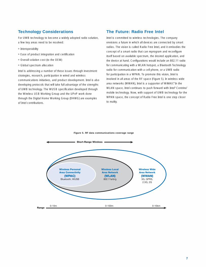
Technology ConsiderationsFor UWB technology to become a widely adopted radio solution,
a few key areas need to be resolved:
Interoperability
Ease of product integration and certification
Overall solution cost (to the OEM)
Global spectrum allocation
Intel is addressing a number of these issues through investment
strategies, research, participation in wired and wireless
communications initiatives, and product development. Intel is also
developing protocols that will take full advantage of the strengths
of UWB technology. The WUSB specification developed through
the Wireless USB Working Group and the UPnP work done
through the Digital Home Working Group (DHWG) are examples
of Intel contributions.
The Future: Radio Free IntelIntel is committed to wireless technologies. The company
envisions a future in which all devices are connected by smart
radios. The vision is called Radio Free Intel, and it embodies the
concept of a smart radio that can reprogram and reconfigure
itself based on available spectrum, the desired application, and
the device at hand. Configurations would include an 802.11 radio
for communicating with a WLAN hotspot, a Bluetooth Technology
radio for communication with a cell phone, or a UWB radio
for participation in a WPAN. To promote this vision, Intel is
involved in all areas of the RF space (Figure 5). In wireless wide
area networks (WWAN), Intel is a supporter of WiMAX*. In the
WLAN space, Intel continues to push forward with Intel® Centrino™
mobile technology. Now, with support of UWB technology for the
WPAN space, the concept of Radio Free Intel is one step closer
to reality.
7
Wireless PersonalArea Connectivity
(WPAC)Bluetooth, WUSB
Wireless LocalArea Network
(WLAN)802.11a/b/g
Wireless WideArea Network
(WWAN)3G, GPRS,2.5G, 2G
Short-Range Wireless
Range0-10m 0-100m 0-10km
Figure 5. RF data communications coverage range
INFORMATION IN THIS DOCUMENT IS PROVIDED IN CONNECTION WITH INTEL® PRODUCTS. NO LICENSE, EXPRESS OR IMPLIED, BY ESTOPPEL OR OTHERWISE, TO ANY INTELLECTUALPROPERTY RIGHTS IS GRANTED BY THIS DOCUMENT. EXCEPT AS PROVIDED IN INTEL’S TERMS AND CONDITIONS OF SALE FOR SUCH PRODUCTS, INTEL ASSUMES NO LIABILITYWHATSOEVER, AND INTEL DISCLAIMS ANY EXPRESS OR IMPLIED WARRANTY, RELATING TO SALE AND/OR USE OF INTEL® PRODUCTS INCLUDING LIABILITY OR WARRANTIESRELATING TO FITNESS FOR A PARTICULAR PURPOSE, MERCHANTABILITY, OR INFRINGEMENT OF ANY PATENT, COPYRIGHT OR OTHER INTELLECTUAL PROPERTY RIGHT. INTELPRODUCTS ARE NOT INTENDED FOR USE IN MEDICAL, LIFE SAVING, OR LIFE SUSTAINING APPLICATIONS.
INTEL MAY MAKE CHANGES TO SPECIFICATIONS AND PRODUCT DESCRIPTIONS AT ANY TIME, WITHOUT NOTICE. ALL PRODUCTS, DATES, AND FIGURES SPECIFIED ARE PRELIMINARYBASED ON CURRENT EXPECTATIONS, AND ARE SUBJECT TO CHANGE WITHOUT NOTICE. INTEL, PROCESSORS, CHIPSETS AND BOARDS MAY CONTAIN DESIGN DEFECTS OR ERRORSKNOWN AS ERRATA, WHICH MAY CAUSE THE PRODUCT TO DEVIATE FROM PUBLISHED SPECIFICATIONS. CURRENT CHARACTERIZED ERRATA ARE AVAILABLE ON REQUEST.
* Other names and brands may be claimed as the property of others.Copyright © 2005 Intel Corporation. All rights reserved.Intel, the Intel logo, and Intel Centrino are trademarks or registered trademarks of Intel Corporation or its subsidiaries in the United States and other countries.
Printed in USA. 0205/MLG/HBD/PDF Please Recycle 300982-002 US
ConclusionUWB and the associated networking protocol efforts are in
the early stages of development, and several key deployment
scenarios are being defined and evaluated. UWB complements
currently deployed wireless networks in the WLAN environment,
plus it extends high bit-rate, multimedia connectivity to WPANs
supporting PC, CE and cellular devices. This combination will
enable true convergence of computers, consumer electronics
and mobile communications.
A common radio platform that connects seamlessly with the
existing networking protocols and cost effectively enables
connectivity solutions among CE peripherals will shift the home
entertainment environment. It will enable multiple usage models
from cable replacement to the streaming of video, audio, and
other entertainment media.
Many UWB components and systems are already in the testing
and demonstration phases, with actual release dates for final
consumer products expected in early 2005. Intel Corporation is
working with the industry to enable this exciting technology and
help ensure its success.