a cmos integrated cc-isfet device for water quality...
TRANSCRIPT

A CMOS Integrated CC-ISFET Device for Water Quality
Monitoring
Pawan Whig1 and Prof. Syed Naseem Ahmad 2
1 Research Scholar, Department of Electronics and Communication Engineering, Jamia Millia Islamia,
New Delhi-110025 India
2 Department of Electronics and Communication Engineering, Jamia Millia Islamia,
New Delhi-110025 India
Abstract This study presents a performance analysis of low power CMOS
Integrated “Current Conveyor Ion Sensitive Field Effect
transistor” (CC-ISFET). The study’s main focus is on simulation
of power and performance analysis of ISFET device, which is
used for water quality monitoring. This approach can improve
calibration of device to a fairly wide range without the use of a
high speed digital processor. The conventional devices generally
used, consume high power and are not stable with temperature
and frequency variations for long term monitoring. The
conventional device [1] has a drawback of low value of slew rate,
high power consumption, and non linear characteristics but in
this novel design, the device exhibits a better slew rate, piece-
wise linear characteristics, and seen consuming low power of the
order of 5.7µW. The functionality of the circuit is tested using
Tanner simulator version 15 for a 70nm CMOS process model.
Very high speed integrated circuit Hardware description
language (VHDL) code for the same scheme is simulated on
Xilinx ISE 10.1 and various simulation results are obtained. The
proposed circuit reduces total power consumption per cycle,
increases speed of operation, fairly linear and is simple to
implement.This device has a simple architecture, and hence is
very suitable for water quality monitoring applications.
Keywords: Slew rate, Calibration, Simulation, Monitoring, Ion
Sensitive Field Effect Transistor, Simulation, Current
Conveyors, Frequency compensation, Low power.
1. Introduction
Monitoring the pH of water resources for water pollution is
a typical and necessary task in today’s overdeveloped
scenario. The normal pH for surface water systems is 6.5-
8.5 and for ground water system 6-8. Water with low pH is
acidic, corrosive and contains several toxic materials
which are very dangerous for health, but the water having
pH more than 8.5 is called hard water which does not
contain harmful materials but the long use of such kind of
water can cause many problems [2]. With the invention of
ISFET [3] there has been a rapid development of pH
Measurement Instruments [4]. With the further
advancement of semiconductor technology ISFET emerged
as a standard device. In spite of the fact that ISFET Sensor
has been developed 30 years ago [5], several drawback of
ISFET sensor remained unsolved, such as phenomena of
fluctuation with time and temperature variations. This
causes in drift in the pH values, and result in poor and slow
response of the device. The second phenomenon is pH
dependent Temperature Coefficient and non linear
temperature dependent mobility in MOSFETS of ISFET
device. Also it was observed that in ISFET drift rate has an
exponential incremental tendency with pH values as well
as Temperature. In Urban water supply system, the water
quality determining indices such as pH value and turbidity
are monitored continuously. When the indices exceed the
limiting value, the system will effectively handle the
treatment against deterioration ensuring the safety of water.
Water is vital for all known forms of life. Many research
works have contributed to design water quality measuring
devices. But it has always been a challenge to find a
precise and accurate device for monitoring the quality of
water. The concept of p[H] was first introduced by Danish
chemist Soren Peder Lauritz Sorensen at the Carlsberg
Laboratory in 1909 and revised to the modern pH in 1924
after it became apparent that electromotive force in cells
depended on activity rather than concentration of hydrogen
ions. The pH is a measure of the acidity or basicity of an
aqueous solution. The use of micro sensors for infield
monitoring of environmental parameters is gaining interest
due to their advantages over conventional sensors. In the
field of micro sensors for environmental applications, Ion
Selective Field Effect Transistors (ISFETs) has proved to
be of special application. They are particularly helpful for
measuring pH and other ions in small volumes and they
can be integrated in compact flow cells for continuous
measurements and monitoring [6]. Pure water is said to be
neutral, with a pH close to 7.0 at 25 °C (77 °F). Solutions
with a pH less than seven (7) are said to be acidic and
IJCSI International Journal of Computer Science Issues, Vol. 9, Issue 4, No 2, July 2012 ISSN (Online): 1694-0814 www.IJCSI.org 365
Copyright (c) 2012 International Journal of Computer Science Issues. All Rights Reserved.
solutions with a pH greater than seven (7) are basic or
alkaline.
1.1 ISFET
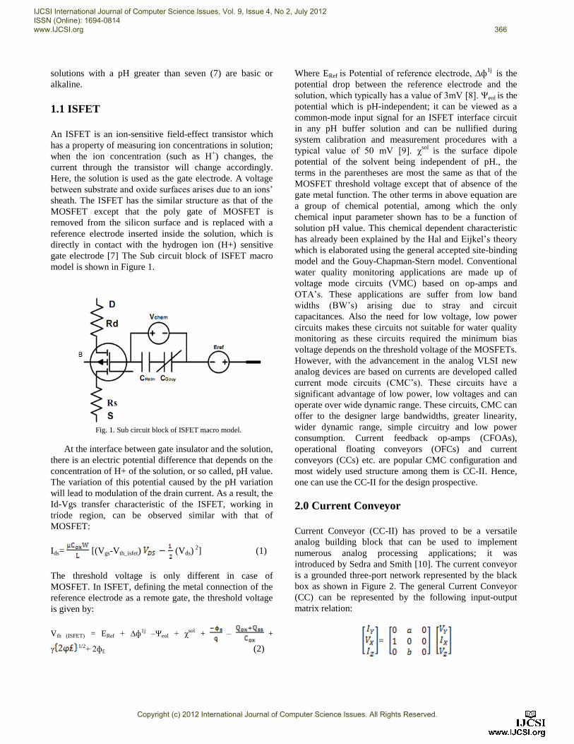
An ISFET is an ion-sensitive field-effect transistor which
has a property of measuring ion concentrations in solution;
when the ion concentration (such as H+) changes, the
current through the transistor will change accordingly.
Here, the solution is used as the gate electrode. A voltage
between substrate and oxide surfaces arises due to an ions’
sheath. The ISFET has the similar structure as that of the
MOSFET except that the poly gate of MOSFET is
removed from the silicon surface and is replaced with a
reference electrode inserted inside the solution, which is
directly in contact with the hydrogen ion (H+) sensitive
gate electrode [7] The Sub circuit block of ISFET macro
model is shown in Figure 1.
Fig. 1. Sub circuit block of ISFET macro model.
At the interface between gate insulator and the solution,
there is an electric potential difference that depends on the
concentration of H+ of the solution, or so called, pH value.
The variation of this potential caused by the pH variation
will lead to modulation of the drain current. As a result, the
Id-Vgs transfer characteristic of the ISFET, working in
triode region, can be observed similar with that of
MOSFET:
Ids= [(Vgs-Vth_isfet) (Vds) 2] (1)
The threshold voltage is only different in case of
MOSFET. In ISFET, defining the metal connection of the
reference electrode as a remote gate, the threshold voltage
is given by:
Vth (ISFET) = ERef + ∆ф1j –Ψeol + χsol + – +
γ 1/2+ 2ф£ (2)
Where ERef is Potential of reference electrode, ∆ф1j
is the
potential drop between the reference electrode and the
solution, which typically has a value of 3mV [8]. Ψeol is the
potential which is pH-independent; it can be viewed as a
common-mode input signal for an ISFET interface circuit
in any pH buffer solution and can be nullified during
system calibration and measurement procedures with a
typical value of 50 mV [9]. χsol
is the surface dipole
potential of the solvent being independent of pH., the
terms in the parentheses are most the same as that of the
MOSFET threshold voltage except that of absence of the
gate metal function. The other terms in above equation are
a group of chemical potential, among which the only
chemical input parameter shown has to be a function of
solution pH value. This chemical dependent characteristic
has already been explained by the Hal and Eijkel’s theory
which is elaborated using the general accepted site-binding
model and the Gouy-Chapman-Stern model. Conventional
water quality monitoring applications are made up of
voltage mode circuits (VMC) based on op-amps and
OTA’s. These applications are suffer from low band
widths (BW’s) arising due to stray and circuit
capacitances. Also the need for low voltage, low power
circuits makes these circuits not suitable for water quality
monitoring as these circuits required the minimum bias
voltage depends on the threshold voltage of the MOSFETs.
However, with the advancement in the analog VLSI new
analog devices are based on currents are developed called
current mode circuits (CMC’s). These circuits have a
significant advantage of low power, low voltages and can
operate over wide dynamic range. These circuits, CMC can
offer to the designer large bandwidths, greater linearity,
wider dynamic range, simple circuitry and low power
consumption. Current feedback op-amps (CFOAs),
operational floating conveyors (OFCs) and current
conveyors (CCs) etc. are popular CMC configuration and
most widely used structure among them is CC-II. Hence,
one can use the CC-II for the design prospective.
2.0 Current Conveyor
Current Conveyor (CC-II) has proved to be a versatile
analog building block that can be used to implement
numerous analog processing applications; it was
introduced by Sedra and Smith [10]. The current conveyor
is a grounded three-port network represented by the black
box as shown in Figure 2. The general Current Conveyor
(CC) can be represented by the following input-output
matrix relation:
=
IJCSI International Journal of Computer Science Issues, Vol. 9, Issue 4, No 2, July 2012 ISSN (Online): 1694-0814 www.IJCSI.org 366
Copyright (c) 2012 International Journal of Computer Science Issues. All Rights Reserved.

When a=1, the first generation current conveyor
(commonly denoted CCI) is obtained. For a=0, we obtain
the second generation current conveyor (commonly
denoted CCII). For a=-1 we obtain the third generation
current conveyor (commonly denoted CCIII). Usually,
b=±1. The sign of the b parameter determines the conveyor
current transfer polarity. Positive b indicates that the CC
has a positive current transfer ratio and is denoted by
CCI+, CCII+ or CCIII+ while negative b means that it has
a negative current transfer ratio and is denoted by CCI-,
CCII-or CCIII-
Fig. 2. Block diagram current conveyor
A well-known basic building block is the second
generation current conveyor (CCII). Second generation
current conveyors are widely used by analog designers. An
important attribute of current conveyor is its ability to
convey current between two terminals (X and Z) at vastly
different impedance levels.
2.1 CCISFET For the integrated sensor, the measurement circuit tracks
the threshold voltage (or the flat-band voltage) of the
ISFET as the electrolyte pH is varied. A practical solution
to integrate the sensor with electronics is to view the
ISFET sensor as a circuit component in an integrated
circuit rather than as an add-on sensor whose output signal
is further processed. In this paper, the ISFET is used as
one of the input transistors in the differential stage of the
current conveyor as shown in Figure 3. The circuit
functions as follows: when the ISFET-Current Conveyor is
configured as a voltage follower, the output voltage (Vo) is
equal to the input voltage (Vin); any difference in
threshold voltages and bias currents between the two input
transistors at the differential input stage will also appear at
the output.
Fig. 3. CCISFET device
3.0 Simulation and Observations
Simulation of a device for water quality monitoring
device using CCISFET involving second generation
current conveyors have been carried out on Tanner
simulator version 15 for a 70nm CMOS process model
shown in Figure 4.The output response of the device with
respect to the time i.e transient analysis shown in Figure 6
justify the device is highly linear and having better slew
rate than the conventional device . The power results
obtained when the device is simulated 70nm technology is
shown in the appendix at the end of the paper and it is
found that the device consumes the average power of 5.7
µW watts.
Fig. 4. Circuit diagram of device
IJCSI International Journal of Computer Science Issues, Vol. 9, Issue 4, No 2, July 2012 ISSN (Online): 1694-0814 www.IJCSI.org 367
Copyright (c) 2012 International Journal of Computer Science Issues. All Rights Reserved.
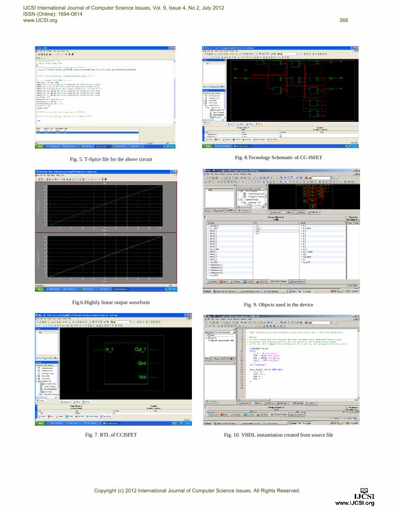
Fig. 5. T-Spice file for the above circuit
Fig.6.Highily linear output waveform
Fig. 7. RTL of CCISFET
Fig. 8.Tecnology Schematic of CC-ISFET
Fig. 9. Objects used in the device
Fig. 10. VHDL instantiation created from source file
IJCSI International Journal of Computer Science Issues, Vol. 9, Issue 4, No 2, July 2012 ISSN (Online): 1694-0814 www.IJCSI.org 368
Copyright (c) 2012 International Journal of Computer Science Issues. All Rights Reserved.

Table 1. Transient analysis
Table 2. Device process parameters
Process Parameters
Power Supply (V) 5
Load Regulation 3.93
Line Regulation(m) 0.6
Current range (µA) 1-50
Average Power Consumed
(W)
1.126179e-005
Max Power(W) 0.574213e-005
Above Table-1 describe the transient behavior of the input
with the output and Table-2 describe the various device
process parameters including power supply, Load
regulation, Line Regulation, Current range, Average power
consumed, Max Power.
Fig. 11.Power Comparison Chart
Fig. 12. Component Comparison Chart
Table3: Result analysis of various schemes
Parameters Conventional
Device
New
Device
Technology CMOS CMOS
Power
supply(VDD,
GND)
5V-0V 5V-0V
No. of Mosfets 27 16
Capacitor 2 2
Current Source 4 3
NMOS 17 10
PMOS 10 6
Resistor 5 5
Voltage Source 4 2
Average power
dissipation
(Watts)
1.304338e-005 1.126179e-
005
Max power
(Watts) 1.635414e-005
0.574213e-
005
Min power
(Watts) 0000000e-000
0.131296e-
005
Stability
analysis
Closed loop
Stable
Closed loop
Stable
Inference from table 3: For the same technology i.e. CMOS technology deployed
for all the four analog IC’s and the same power supply we
arrive at the following comparative results:
a. Number of MOSFET’s is 27 in Conventional
device, 16 in New device, Later deploys 37% of
components over 63% used in the previous one
shown in Fig. 12.
b. Number of capacitors remains constant in both
techniques.
c. Number of current sources deployed is 4 in
Conventional device and 3 in new device.
d. Number of n-MOS and p-MOS required are as
follows: 17 and 10 for Conventional device, 10
and 6 for new device. From these numbers we can
figure out that there is significant saving in terms
of Components.
e. Number of resistors required for both cases are
same.
f. Voltage source require for proper operation of
the devices are 4 for Conventional device and 2 in
new device.
g. The average power dissipation in watts is listed
for the two cases:
1. Conventional device - 1.304338e-005
2. New device - 1.126179e-005
IJCSI International Journal of Computer Science Issues, Vol. 9, Issue 4, No 2, July 2012 ISSN (Online): 1694-0814 www.IJCSI.org 369
Copyright (c) 2012 International Journal of Computer Science Issues. All Rights Reserved.

Form this we come down to the conclusion that the average
power dissipated in the later case is less.
h. Maximum power dissipated in watts is listed for
the four cases:
1. Conventional device - 1.635414e-005
2. New device - 0.574213e-005
From this we come down to the conclusion that the
maximum power consumption in case of new device is
26% as compared to conventional device which consumes
74%. Hence there is total 48% power saving shown in Fig.
11.
4.0 Result and Conclusion
In this novel design, a new device employing second
generation current conveyors (CCIIs) is proposed. The
second-generation current conveyor introduced is a
convenient building block that provides a simplified
approach to the design of linear analog systems. It also
consumes considerably low power of the order of 5.7 µW
compared to [1]. There is significant improvement in the
slew rate. The output observed in Fig 6 is highly linear. A
significant advantage of the proposed design is it’s simple
architecture, and low component count a saving of 26% as
compared to [1]. Therefore it is very suitable for water
quality monitoring applications. VHDL code for the device
is simulated on Xilinx ISE 10.1 software and RTL
schematic is shown in fig 7. This study may be extended
for further improvements in terms of power and size,
besides the wiring and layout characteristics level.
References
[1] Pawan Whig, S. N. Ahmad, (2011) On the Performance of ISFET-based Device for Water Quality Monitoring. Int'l J. of Communications, Network and System Sciences ISSN 1913-3715, pp:709 -719.
[2] [Online].Available:http://www.freedrinkingwater.com/water-
education/quality-water-ph.htm.
[3] P.Bergveld (1970), Development of an Ion-sensitive Solid-state
Device for Neurophysiologic Measurements, IEEE Trans. Biomed.
Eng.pp: 70-71.
[4] Cecilia Jimenez-Jorquera, Jahir Orozoo, Antoni Baldi (2010),
ISFET based Microsensors for Environmental Monitoring, Journal
of Sensors ISSN 1424-8220, pp: 61-83.
[5] P.Bergveld,(2000) “Thirty years of ISFETOLOGY what happened
in the past 30 years and what may happen in the next 30
years,’Sens.Actuators B, Vol . 88,pp1-20.
[6] Chang, Y.-H.; Lu, Y.-S.; Hong, Y.-L.; Gwo, S.; Yeh, J. A. (2011);
“Highly Sensitive pH Sensing Using an Indium Nitride Ion-
Sensitive Field-Effect Transistor.” Vol: 11, Issue: 5, pp: 1157-
1161.
[7] D.MWilson,S.Hoyt,J.Janata,K.Booksh,andL.obando,(2001)”Chemi
cal sensors for portable ,handheld field instruments,’IEEE Sensors
j.,vol.1,no.4,pp256-274.
[8] S.jamasb,S.D. Collins , and R.L Smith(1998) ,”A physical model
for threshold voltage insability in SI3N4 gate H+ sensitive
FETs,”IEEE Tran. Electron Devices, Vol. 45 no. 6 ,pp.1239-1245.
[9] L.J Bousse,D.Hafeman, and N.Tran(1991),’Time Dependence of
the chemical response of silicon nitride surfaces ,”Sens. Actuators
B,Vol.1,pp.361-367. [10] A Sedra, K. A Smith (1970). second-generation conveyor and its
applications,IEEE Transconductions on Circuit Theory. 1970, CT-17,pp: 132-134.
[11] Pawan Whig, S. N. Ahmad, (2011) Performance analysis and frequency Compensation Technique for Low Power Water Quality Monitoring Device Using ISFET Sensor. International Journal of Mobile and Adhoc Network
Appendix ======================================
* Synthesis Options Summary *
======================================
---- Source Parameters
Input File Name "Cell3.prj"
Input Format mixed
Ignore Synthesis Constraint File : NO
---- Target Parameters
Output File Name : Cell3
Output Format : NGC
Target Device : xc3s100e-5-
vq100
---- Source Options
Top Module Name : Cell3
Automatic FSM Extraction : YES
FSM Encoding Algorithm : Auto
FSM Style : lut
RAM Extraction : Yes
RAM Style : Auto
ROM Extraction : Yes
Mux Style : Auto
Decoder Extraction : YES
Priority Encoder Extraction : YES
Shift Register Extraction : YES
Logical Shifter Extraction : YES
XOR Collapsing : YES
ROM Style : Auto
Mux Extraction : YES
Resource Sharing : YES
Asynchronous To Synchronous : NO
Multiplier Style : auto
Automatic Register Balancing : No
---- Target Options
Add IO Buffers : YES
Global Maximum Fanout : 500
Add Generic Clock Buffer(BUFG) : 24
Register Duplication : YES
IJCSI International Journal of Computer Science Issues, Vol. 9, Issue 4, No 2, July 2012 ISSN (Online): 1694-0814 www.IJCSI.org 370
Copyright (c) 2012 International Journal of Computer Science Issues. All Rights Reserved.

Slice Packing : YES
Use Clock Enable : Yes
Use Synchronous Set : Yes
Use Synchronous Reset : Yes
Pack IO Registers into IOBs : auto
Equivalent register Removal : YES
---- General Options
Optimization Goal : Speed
Optimization Effort : 1
Library Search Order : Cell3.lso
Netlist Hierarchy :
as_optimized
RTL Output : Yes
Global Optimization :
AllClockNets
Read Cores : YES
Hierarchy Separator : /
Bus Delimiter : <>
Case Specifier : maintain
Slice Utilization Ratio : 100
BRAM Utilization Ratio : 100
Verilog 2001 : YES
Auto BRAM Packing : NO
Slice Utilization Ratio Delta : 5
======================================
* Final Report *
======================================
Final Results
RTL Top Level Output File Name : Cell3.ngr
Top Level Output File Name : Cell3
Output Format : NGC
Optimization Goal : Speed
Keep Hierarchy : NO
Design Statistics
# IOs : 4
Cell Usage :
# BELS : 1
# GND : 1
# IO Buffers : 4
# IBUF : 1
# OBUF : 3
# Others : 28
# Capacitor : 2
# CurrentSource : 3
# NMOS : 10
# PMOS : 6
# Resistor : 5
# VoltageSource : 2
======================================
*SEDIT: Alter blocks = 0
* General options:
* Device and node counts:
* MOSFETs - 11 MOSFET geometries - 4
* BJTs - 0 JFETs - 0
* MESFETs - 0 Diodes - 0
* Capacitors - 1 Resistors - 0
* Inductors - 0 Mutual inductors - 0
* Transmission lines - 0 Coupled transmission lines - 0
* Voltage sources - 4 Current sources - 0
* VCVS - 0 VCCS - 0
* CCVS - 0 CCCS - 0
* V-control switch - 0 I-control switch - 0
* Macro devices - 0 External C model instances - 0
* HDL devices - 0
* Sub circuits - 0 Sub circuit instances - 0
* Independent nodes - 6 Boundary nodes - 5
* Total nodes - 11
Power Report
Power Results
vdd from time 0 to 1e-008
Average power consumed -> 1.626179e-005 watts
Max power 0.574213e-005at time 5e-009
Min power 1.31296e-005 at time 5e-009
Authors Pawan Whig is born in India (New Delhi) on13 June
1980. He received the B.Tech (ECE) in 2005 from MAIT
under GGSIPU and M.Tech in VLSI from CDAC NOIDA
in 2008. He is currently a Research Scholar in ECE
department at Jamia Millia Islamia. He is working on
Readout circuit for various sensor devices. His research
interest is simulation and design, Modeling and Process
Technology.
Prof. (Dr.) Syed Naseem Ahmad is currently working as
a Head of Department (ECE) at Jamia Milia Islamia
University, Jamia Nagar India; New Delhi-110025. He did
bachelor in electrical engineering in 1975 from
Aligarh Muslim University. He did his M.Tech degree
from the same university in Instrumentation and Control
engineering in 1978. He has done PhD from JMI. He has
wide area of research ranging from Analog Signal
Processing, Image processing and communication
engineering. He has guided many research fellows He has
several papers in national and international journals.
IJCSI International Journal of Computer Science Issues, Vol. 9, Issue 4, No 2, July 2012 ISSN (Online): 1694-0814 www.IJCSI.org 371
Copyright (c) 2012 International Journal of Computer Science Issues. All Rights Reserved.