a cell-based design methodology for synthesizable rf
TRANSCRIPT

A Cell-Based Design Methodology for Synthesizable RF/Analog Circuits
by
Young Min Park
A dissertation submitted in partial fulfillment
of the requirements for the degree of Doctor of Philosophy
(Electrical Engineering) in The University of Michigan
2011
Doctoral Committee:
Assistant Professor David D. Wentzloff, Chair Professor Dennis Michael Sylvester Associate Professor Michael Flynn Associate Professor Vineet Rajendra Kamat
Acknowledgments
Firstly, I want to thank my research advisor, Professor David Wentzloff. He helped me
establish a direction of research and solve numerous problems during the course, by
providing technical guidance and unending encouragement. His support and advice,
however, were not limited to research, and he has been a great mentor in many aspects
throughout my Ph.D. Without him, this process would have been much harder, and I was
very fortunate to have him as my research advisor. I’d also like to thank Professor Dennis
Sylvester, Professor Michael Flynn, and Professor Vineet Kamat for serving on my thesis
committee. Their review and helpful advice during the meetings improved this thesis, and
their time on the committee will be always appreciated.
I want to thank my group members, Sangwook Han, Dae Young Lee, Jonathan Brown,
Seunghyun Oh, Kuo-Ken Huang, Osama Khan, Muhammad Faisal, and Nathan Roberts.
We have encouraged each other, and shared ideas to solve problems in the lab and in the
office. However, we never missed opportunities to have break from work, and promote our
friendship. I really enjoyed the time with these great group members.
I also want to thank the Kwanjeong Educational Foundation for their financial support
for my graduate study.
I want to thank my parents, Jaeho Park and Sukhee Lee, my parents-in-law, Yoonsik Min
and Hoisun Kim, my sister, Youngeun Park, and extended family for their support. Most of
all, I am really grateful to my wife, Sunghwa Min, and my son, Sean Siwoo Park. They
ii

always make me smile, which has been the best encouragement to me. Without their
support, I could not survive this process.
iii

Table of Contents
Acknowledgments ............................................................................................................. ii List of figures ................................................................................................................... vii List of Tables ................................................................................................................... xii Abstract ........................................................................................................................... xiii Chapter 1. Introduction ....................................................................................................................1
1.1. Background ...............................................................................................................1
1.1.1. Digital vs. Analog in nanometer-scale CMOS Technology ...............................1
1.1.2. Digitally Assisted Architectures .........................................................................2
1.1.3. All-Digital Architectures ....................................................................................5
1.2. Cell-Based Circuit Design ........................................................................................8
1.3. Applications of Cell-Based Design ........................................................................11
1.4. Primary Contributions ............................................................................................12 2. Cell-Based Digitally Controlled Oscillator ...............................................................15
2.1. Introduction ............................................................................................................15
2.2. Cell-Based DCO: Structure and Properties .............................................................16
2.3. Calibration of DCO .................................................................................................20
2.4. Modeling of Cell-Based DCO Performance ..........................................................25
iv

2.4.1. Timing Model Based on Effective Drive Strength ..........................................26
2.4.2. Modeling of coefficients and Effective Drive Strength ..................................28
2.5. Experimental Results ..............................................................................................35
2.6. Summary ................................................................................................................36
3. All-Digital Synthesizable UWB Transmitter ............................................................38
3.1. Introduction ............................................................................................................38
3.2. UWB Transmitter Architecture ..............................................................................39
3.2.1. Digitally Controlled Oscillator with Tunable Delay Cells ..............................41
3.2.2. Pulse Width Delay Line ...................................................................................42
3.2.3. Scrambler .........................................................................................................44
3.3. Calibration of UWB Center Frequency ..................................................................45
3.4. Measured UWB Transmitter Performance .............................................................49
3.5. Summary ................................................................................................................55 4. All-Digital Synthesizable Time-to-Digital Converter ..............................................57
4.1. Introduction ............................................................................................................57
4.2. Cyclic Vernier Time-to-Digital Converter .............................................................59
4.2.1. TDC Architecture ............................................................................................59
4.2.2. Digitally Controlled Oscillator ........................................................................61
4.2.3. Edge Detector ..................................................................................................62
4.3. TDC Calibration Utilizing Mismatch .....................................................................64
4.4. TDC Performance ...................................................................................................68
v
vi
4.4.1. TDC Measurement ..........................................................................................69
4.4.2. Rising/falling Edge Detection and TDC in ADPLL ........................................71
4.4.3. Power ...............................................................................................................74
4.5. Summary ................................................................................................................75 5. All-Digital Synthesizable PLL ...................................................................................77
5.1. Introduction ............................................................................................................77
5.2. ADPLL Architecture ..............................................................................................78
5.3. Circuit Implementation ..........................................................................................79
5.3.1. DCO and DCO controller ................................................................................79
5.3.2. Time to digital converter .................................................................................84
5.3.3. Prescaler ..........................................................................................................85
5.3.4. Digital loop filter .............................................................................................86
5.3.5. Divider .............................................................................................................87
5.3.6. Linear model of ADPLL .................................................................................88
5.4. Measurement Results .............................................................................................91
5.5. Summary ................................................................................................................92 6. Conclusions ..................................................................................................................94 Bibliography .....................................................................................................................97

List of Figures Fig. 1.1. Energy-equivalent number of logic gates as a function of digital feature size and ADC resolution in bits [6] ..................................................................................................2 Fig. 1.2. Digitally assisted ADC [60] ................................................................................3 Fig. 1.3. Area and Power of post-processor [60] ...............................................................3 Fig. 1.4. Digital predistortion for power amplifier [14] .....................................................4 Fig. 1.5. Frequency synthesizer with digital calibration technique [67] ............................4 Fig. 1.6. Block diagram of all-digital UWB transmitter [21] ............................................6 Fig. 1.7. Block diagram of all-digital GSM transmitter [26] .............................................7 Fig. 1.8. Proposed cell-based design flow ........................................................................10 Fig. 1.9. Micrograph and layout view of cell-based designed UWB transmitter in 65nm CMOS ...............................................................................................................................11 Fig. 2.1. Digitally controlled oscillator with tri-state buffers from standard cell library .17 Fig. 2.2. Simulated periods of three-stage DCO with different number of buffers (N) ...18 Fig. 2.3. Description of automatically P&R-ed buffers in a three-stage DCO and wire network between stages ....................................................................................................19 Fig. 2.4. Simulated incremental period in a stage of DCO with N=32 .............................20 Fig. 2.5. Measured period by turning off each buffer in a stage ......................................21 Fig. 2.6. Measured incremental period by turning off each buffer in a stage ..................21 Fig. 2.7. Coarse/fine frequency control using sorted buffer list and measured frequency control ...............................................................................................................................22
vii

Fig. 2.8. Measured incremental period of buffers in stage 3 over different supply voltages (upper, 0.95V, 1V, and 1.05V) and over different temperatures (lower, 0°C, 25°C, and 70°C) .................................................................................................................................23 Fig. 2.9. Measured incremental period over 13 chips ......................................................23 Fig. 2.10. Measured standard deviation of incremental periods divided by mean of incremental periods for each buffer ..................................................................................24 Fig. 2.11. Measured incremental periods at different supply voltages (6 chips at 0.9V, 4 chips at 0.8V, and 2 chips at 0.7V) ...................................................................................25 Fig. 2.12. Measured and modeled periods of DCO over different configurations ..........27 Fig. 2.13. Example placement in three-stage DCO with N=32 .......................................28 Fig. 2.14. Coefficients and constant over simplified load model ....................................29 Fig. 2.15. Minimum period over simplified load model ..................................................30 Fig. 2.16. Constant current source model for interconnect ...............................................32 Fig. 2.17. Multiple current sources to a sink .....................................................................32 Fig. 2.18. Constant current source model .........................................................................33 Fig. 2.19. Simplified wire length model ..........................................................................34 Fig. 2.20. Comparison between effective drive strengths from measurement and model 35 Fig. 2.21. Cumulative sum of effective drive strength from measurement and model .....36 Fig. 3.1. Block diagram of proposed UWB transmitter ...................................................40 Fig. 3.2. Digitally controlled oscillator embedding tunable delay cells ..........................41 Fig. 3.3. Delay line embedding tunable delay cells .........................................................42 Fig. 3.4. Measured programmable pulse width range. By turning off tri-state buffers in the delay line, the pulse width is increasing ...........................................................................43 Fig. 3.5. Delay-based BPSK scheme with scrambler ......................................................44 Fig. 3.6. Description of cell-based layout and measured incremental periods of buffers in stage1 ................................................................................................................................46
viii

Fig. 3.7. Description of calibration scheme with sorted lists ...........................................46 Fig. 3.8. Measured frequency control with sorted lists in DCO employing delay cells with 64 buffers, operating at 1V (top), and DCO employing delay cells with 32 buffers, operating at 0.9V (bottom) ................................................................................................47 Fig. 3.9. Measured incremental period of buffers in stage 1 over 4 different chips ........48 Fig. 3.10. Measured incremental period of buffers in stage 1 over different supply voltages (top, 0.85V, 0.9V, and 0.95V), and over different temperatures (bottom, -40°C, 25°C, and 80°C) .................................................................................................................................49 Fig. 3.11. 65nm CMOS transmitter die micrograph and layout view ..............................50 Fig. 3.12. Measured transient waveform of UWB pulse at 3.5GHz after off-chip high-pass filter ...................................................................................................................................50 Fig. 3.13. Measured output spectral densities of three channels after off-chip high-pass filter ...................................................................................................................................51 Fig. 3.14. Measured power spectral densities w/ and w/o scrambling. Without scrambling, PSD violates the FCC mask ..............................................................................................51 Fig. 3.15. Measured output amplitude before/after filter of 13 chips. These are attenuated values (1dB) by cable in measurement .............................................................................52 Fig. 3.16. Measured temperature variation of center frequency control ..........................53 Fig. 3.17. Measured frequency control of 13 chips .........................................................54 Fig. 3.18. Measured active energy/pulse at four different pulse widths from 1.1ns (1.4GHz bandwidth) to 2.6ns (500MHz bandwidth) .......................................................................54 Fig. 4.1. General block diagram of all digital PLL ...........................................................58 Fig. 4.2. (a) Block diagram of the proposed TDC and (b) timing diagram ......................59 Fig. 4.3. Digitally controlled oscillator with tri-state buffers. The buffers from standard cell library are automatically placed-and-routed .....................................................................61 Fig. 4.4. Structure of edge detector ...................................................................................62 Fig. 4.5. Detection of (a) rising and (b) falling edges in the proposed phase detector .....64 Fig. 4.6. Measured incremental period in stage 2 of slow DCO and sorted buffer list ....65
ix

Fig. 4.7. Measured coarse step resolution .........................................................................65 Fig. 4.8. Description of fast DCO calibration ...................................................................66 Fig. 4.9. Measured fine step resolution .............................................................................66 Fig. 4.10. Measured fine step resolution variation over supply voltage (0.9V, 0.95V, 1V, 1.05V, and 1.1V) ...............................................................................................................67 Fig. 4.11. Measured fine step resolution variation over temperature (0°C, 25°C, and 70°C) ............................................................................................................................................67 Fig. 4.12. Micrograph and layout view of TDC ...............................................................69 Fig. 4.13. Coarse and fine measurement of TDC .............................................................70 Fig. 4.14. (a) Single shot measurements over constant inputs with a fine resolution of 5.5ps, (b) standard deviation over a large range of inputs, and (c) standard deviation over sum of coarse/fine codes ...............................................................................................................71 Fig. 4.15. Measurement time reduction by detecting either of rising or falling edge .......72 Fig. 4.16. Calculated output vs. input time difference. In this figure, the offset from input signal paths such as cable and PCB is adjusted. The measured duty cycle is 41%, and the deviation by duty cycle variation is observed ...................................................................72 Fig. 4.17. Application of TDC in ADPLL ........................................................................73 Fig. 5.1. Block diagram of proposed ADPLL ...................................................................79 Fig. 5.2. Block diagram of DCO and control blocks ........................................................80 Fig. 5.3. Calibration algorithm utilizing systematic mismatch .........................................81 Fig. 5.4. Measured DCO frequency control over (a) voltage, (b) temperature, and (c) process variation ...............................................................................................................82 Fig. 5.5. Measured incremental period of buffers in Stage1 over (a) voltage, (b) temperature, and (c) process variation ..............................................................................83 Fig. 5.6. Block diagram of TDC and fine step resolution control ....................................85 Fig. 5.7. Description of prescaler operation ......................................................................86 Fig. 5.8. z-domain model of Digital loop filter (DLF) ......................................................87
x

xi
Fig. 5.9. Structure of counter-based divider .....................................................................87 Fig. 5.10. Linear model of ADPLL ...................................................................................88 Fig. 5.11. Linear model of ADPLL with noise sources ....................................................90 Fig. 5.12. Measured output clock signal and jitter histogram at 2.5GHz (top) and power consumption of ADPLL (bottom) .....................................................................................91 Fig. 5.13. Die micrograph of ADPLL ...............................................................................92

List of Tables Table 3.1. Performance Summary of UWB Transmitter ................................................55 Table 4.1. Performance Summary of TDC .......................................................................75 Table 5.1. Performance Summary of ADPLL .................................................................93
xii

xiii
Abstract
A Cell-Based Design Methodology for Synthesizable RF/Analog Circuits
by
Young Min Park
Chair: David D. Wentzloff
As CMOS processes scale and digital gates become faster, it is practical to implement
precisely-timed digital circuits switching in the GHz range. As a result, traditionally analog
circuits have moved towards mostly-digital designs, utilizing accurate time control and
digital signal processing. Recently published all-digital architectures have shown several
advantages over conventional analog circuits in terms of area, scalability, testability, and
programmability. This thesis proposes a cell-based design methodology for synthesizable
RF/analog circuits, where all functional blocks are not only implemented in all-digital
architectures, but they are also described in a hardware description language, synthesized
from commercial standard cell libraries, and automatically placed and routed using design
tools. This cell-based design procedure significantly shortens the design time, and
enhances portability of the circuits for various applications and different design nodes.

A cell-based digitally controlled oscillator (DCO) is proposed as a core block for
synthesizable circuits. The DCO consists of tri-state buffers from standard cell libraries,
and the frequency of the DCO is digitally controlled by turning on/off the buffers. Instead
of custom layout, the buffers in the DCO are automatically placed and routed (P&R), and
systematic mismatch from automatic P&R is modeled and utilized to characterize the DCO
in the design phase. Calibration schemes utilizing systematic mismatch are also proposed
to achieve higher DCO resolution.
This thesis presents an ultra-wideband (UWB) transmitter, a time-to-digital converter
(TDC), and a PLL in 65nm CMOS technologies as prototypes of cell-based circuits. The
UWB transmitters embed the proposed DCO to control the center frequency and width of
output pulses in the 3.1GHz-5.0GHz UWB band, and the measured active energy
efficiency of the transmitter ranges from 12pJ/pulse to 19pJ/pulse. The TDC adopts a
cyclic Vernier structure, where two DCOs are oscillating with slightly different periods.
The resolution of the TDC is the difference between two periods, which is measured as low
as 8ps. The prototype PLL adopts the TDC and the DCO, and shows 3.2psrms of period
jitter at 2.5GHz output frequency, which is comparable to state-of-the-art full-custom
ADPLLs.
xiv

Chapter 1
Introduction
1.1. Background
1.1.1. Digital vs. Analog in nanometer-scale CMOS Technology
The evolution in CMOS technologies has been mostly driven by demand for digital
circuits. The process scaling has been necessary to meet the requirements on speed,
complexity, circuit density, and power consumption, which all results in reduced cost of
digital computation. With the introduction of nanometer-scale CMOS technologies,
however, analog circuit design faces challenges due to the reduced geometry and limited
supply voltage [1-4]. These challenges include degradation in device matching and
increased power dissipation for comparable analog performance in the advanced processes.
Also, passive components are typically required in analog integrated circuits (ICs);
however, they have not scaled as aggressively as transistors, preventing significant density
improvement of analog ICs.
Fig. 1.1 shows the energy efficiency of digital gates in advanced CMOS processes in
terms of an energy-equivalent number of gates compared to analog-to-digital converters
(ADCs). For example, a single conversion of a 10-bit ADC consumes as much energy as
100,000 digital gates in 90nm CMOS, and the number is expected to be significantly
1

increasing in the following process nodes. According to [5], the relative energy cost of
digital computations has reduced roughly by a factor of ten over the past decade.
Fig. 1.1. Energy-equivalent number of logic gates as a function of digital feature size and ADC resolution in bits [6].
1.1.2. Digitally Assisted Architectures
In this environment where the relative energy consumption of digital computation is low
compared to analog circuits, it is beneficial to use digitally assisted architectures to relax
the complexity of analog circuits, thus saving power consumption, and to take advantage of
digital circuits to compensate for non-idealities from the simplified analog circuits. ADCs
were one of the first to adopt digital signal processing to enhance the performance of
analog circuits in advanced CMOS processes. Some examples of compensation through
digital circuits include linearization and mismatch/error correction [5-12][60]. Fig. 1.2
shows an example of a digitally assisted ADC where a post-processor compensates for
inaccuracy of the ADC [60]. The residue amplifier in the pipeline ADC is replaced with an
2

open loop amplifier, reducing significant amplifier power while the post-processor adds
relatively low power as shown in Fig. 1.3; thus the net power consumption is reduced by
adopting this architecture. Fig. 1.3 also shows that the additional area occupied by the
post-processor is only about 20% of the ADC area.
Fig. 1.2. Digitally assisted ADC [60].
Fig. 1.3. Area and Power of post-processor [60].
Other areas have since followed, such as digitally assisted RF circuits [13][14][61-63],
electronics for audio [15], and others [64][65][67]. Fig. 1.4 shows an example of digital
predistortion for a power amplifier (PA) [14]. In cost-driven applications such as mobile
handsets, implementing a linear PA, which is often inefficient, is not desirable. By
adopting digital predistortion, it is allowed to implement a nonlinear PA which is efficient.
Other analog circuits such as image sensors [64], voltage controlled oscillators (VCOs)
3

[65], and charge pumps [67] (Fig. 1.5) adopt digital calibration schemes to improve
performance, which also can be categorized as digitally assisted architectures. As the
implementation cost of digital circuits, this digital calibration can prevail in analog circuits
to improve the performance.
Fig. 1.4. Digital predistortion for power amplifier [14].
Fig. 1.5. Frequency synthesizer with digital calibration technique [67].
In summary, the digitally assisted architectures move the accuracy burden from analog
circuits to digital circuits. Though these digitally assisted architectures have existed for
decades, the degree and the effect of the architectures has become more promising as
4

process scales, since the relative cost of digital gates is further reduced as discussed in
Section 1.1.1.
1.1.3. All-Digital Architectures
All-digital architectures take further advantage of digital circuits in conventional analog
applications. While the previously discussed architectures use digital gates to compensate
for non-idealities of analog components, in all-digital architectures, analog circuits are
completely replaced by digital circuits where signals are switching between the power
supply voltage and ground. Therefore, the primary operation of all-digital architectures is
different from conventional analog architectures, and the performance is determined by the
timing accuracy of signals rather than the voltage level accuracy. As devices scale, the
switching frequency of logic gates increases, and it improves the timing control of digital
signals. On the other hand, supply voltage in advanced CMOS process is reduced, thereby
limiting voltage headroom for analog operations. Thus, all-digital architectures leverage
the advantages of current processes, and avoid the weakness of them.
All-digital architectures also provide advantages such as testability, flexibility, noise
immunity, and higher levels of integration. The interfaces between blocks are digital
signals; thus they are more observable through testing structures, easier for post-fabrication
control, and more immune to noise in the signal paths. Also, the functional blocks can be
integrated with other digital circuits with the same process options, improving the degree
of integration, and reducing manufacturing cost.
The feasibility of all-digital architectures is also dependent on applications, and an
architectural study is required to determine the feasibility of converting an analog function
5

to an all-digital implementation. The impulse radio ultra-wideband (IR-UWB) transmitter
is one of the applications that fits well with all-digital architectures. The duty-cycled nature
of IR-UWB is advantageous for digital implementation, since there is no static current
except leakage power, thereby minimizing power consumption between pulsed signal
generation. Also, when non-coherent communication is adopted with e.g. an energy
detection receiver [17], the timing accuracy achievable in recent digital circuits is
sufficient for wireless communication with only a <0.1dB degradation in the effective SNR
compared to an ideal implementation. In [18-24], several all-digital UWB transmitters are
presented, and Fig. 1.6 shows the structure of the UWB transmitter in [21]. In the
transmitter in Fig. 1.6, all functional blocks are implemented in a digital process, and pulse
shaping for meeting a spectral mask is achieved through accurate timing control of several
parallel digital paths. One advantage of this architecture is that there is no functional block
which consumes static power, other than leakage current through digital gates, therefore
the transmitter only consumes power when generating a UWB pulse and is idle between
pulses. Low power, low range communication such as specified for 802.15.4a [25] have
Fig. 1.6. Block diagram of all-digital UWB transmitter [21].
6

been target applications for IR-UWB, thus this all-digital architecture can provide low
power and low manufacturing cost due to its small size.
Fig. 1.7. Block diagram of all-digital GSM transmitter [26].
Fig. 1.7 shows the block diagram of a commercial all-digital GSM transmitter [26]. This
transmitter is implemented based on an all-digital PLL (ADPLL), which replaces the
conventional voltage controlled oscillator (VCO), phase/frequency detector (PFD), charge
pump, and loop filter found in an analog PLL with a digitally controlled oscillator (DCO),
time-to-digital converter (TDC), and digital loop filter.
Though the DCO in this transmitter employs passive components such as an inductor and
varactors, the analog structure is abstracted, and interfaced by only digital signals.
Therefore, the functional blocks: (DCO, TDC and digitally controlled power amplifier
(DPA)) are controlled by digital signals, and integrated with other digital logic blocks. This
approach provides smaller silicon area, less power consumption, testability, and a higher
probability of first-time silicon success. All-digital architecture is not a new approach,
where all-digital phase locked loops (ADPLL) were studied decades ago [66], however,
CMOS process scaling has actively motivated this approach recently, achieving
7

performance for target applications comparable to analog counterparts [27-37] as well as
the advantages mentioned above.
1.2. Cell-Based Circuit Design
While all-digital architectures take advantage of digital circuits in advanced CMOS
processes, and address design challenges for analog functions, the circuits still cannot be
absorbed in an automated digital design flow. Digital VLSI circuits such as
microprocessors and DSPs are described in hardware description languages, and
synthesized from a standard cell library of logic gates. The designs are then automatically
placed and routed by powerful CAD tools. The standard cell library consists of pre-defined
digital building blocks (e.g. AND, OR, D-Flipflop gates) which are fully characterized for
performance and the circuit layout is provided in libraries, and CAD tools have been
advanced to fully leverage the standard cell engineering. Thus, the typical design
methodology with standard cells significantly simplifies the circuit implementation. Also,
standard cells can fully take advantage of process scaling. Since standard cell libraries
consist of digital logic gates, the area, power of cell-based circuits only improves through
process nodes. In addition, standard cell libraries provide identical functional cells between
process nodes, or between different process technologies, making cell-based circuits more
scalable and portable.
All-digital transmitters and PLLs in Section 1.1, however, include custom circuit blocks
whose performance is dependent on precise, custom layout which is time consuming and
error prone. These full-custom designs follow separate design flow from synthesized
digital logic blocks in the circuit. This limits the portability and scalability of these
8

partially-custom, all-digital architectures. From the discussion in Section 1.1, it is shown
that each functional block in the all-digital architectures can be abstracted as a digital block,
interfaced with digital signals. If the functional blocks are implemented with standard cells,
the circuits can be synthesized from standard cell libraries. In this thesis, we propose a
cell-based design methodology for synthesizable analog functionality. Fig. 1.8 describes
the proposed design flow for synthesized all-digital analog/RF circuits. Standard digital
logic circuits follow the design flow on the bottom in Fig. 1.8. When the HDL description
is synthesized from a standard cell library, synthesis tools reference the timing analysis in
the library, and compile netlists with standard cells that meet a target speed. Then,
automatic P&R tools place and route the cells based on the timing analysis, incorporating
the impact of additional wiring capacitance. This design flow works for most digital logic
circuits, where only timing constraints in critical paths need to be satisfied. For analog
functions, however, every signal path can affect the performance, and automatic design
flow complicates the timing analysis of the cell-based circuits. Therefore, a modified
design flow is required as shown on the top of Fig. 1.8.
The first step of the proposed design methodology is to convert current building block,
which are analog or full-custom digital blocks, to cell-based functional blocks. In Fig. 1.6
and Fig. 1.7, DCOs are still analog-structured or fully custom digital circuits/layouts. We
propose a cell-based DCO as a core building block in the cell-based design in Chapter 2.
Other blocks are also converted to structured Verilog code or behavioral description in
Verilog. Then, the functional blocks are synthesized from target standard cell libraries, and
placed and routed with automatic design tools with the same process used by standard
digital circuit (e.g. microprocessor).
9
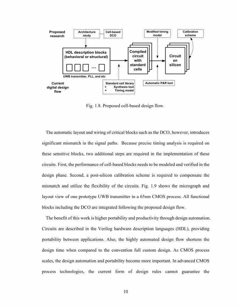
Fig. 1.8. Proposed cell-based design flow.
HDL description blocks(behavioral or structural)
Standard cell library+ Synthesis tool+ Timing model
Modified timing model
Automatic P&R tool
Compiledcircuit with
standardcells
Circuiton
silicon
Calibrationscheme
Architecturestudy
UWB transmitter, PLL, and etc
Proposed research
Currentdigital design
flow
Cell-basedDCO
The automatic layout and wiring of critical blocks such as the DCO, however, introduces
significant mismatch in the signal paths. Because precise timing analysis is required on
these sensitive blocks, two additional steps are required in the implementation of these
circuits. First, the performance of cell-based blocks needs to be modeled and verified in the
design phase. Second, a post-silicon calibration scheme is required to compensate the
mismatch and utilize the flexibility of the circuits. Fig. 1.9 shows the micrograph and
layout view of one prototype UWB transmitter in a 65nm CMOS process. All functional
blocks including the DCO are integrated following the proposed design flow.
The benefit of this work is higher portability and productivity through design automation.
Circuits are described in the Verilog hardware description languages (HDL), providing
portability between applications. Also, the highly automated design flow shortens the
design time when compared to the convention full custom design. As CMOS process
scales, the design automation and portability become more important. In advanced CMOS
process technologies, the current form of design rules cannot guarantee the
10

manufacturability of circuits; thus the design rules become much more complex, or allow
only restricted forms of circuit layout [38]. This degrades the productivity of analog circuit
design and custom digital circuits, making cell-based design more attractive.
Fig. 1.9. Micrograph and layout view of cell-based designed UWB transmitter in 65nm CMOS.
TX
190 µm
190 µm
DCO
DelayLine
Counter
In this research, synthesizable architectures of several applications are presented, and
prototypes are implemented. Calibration schemes are applied to the prototypes, and
performance comparable to full-custom implementations is achieved. Also, a modified
timing model for cell-based DCO is explored to apply to a completely automated design
flow.
1.3. Applications of Cell-Based Design
The cell-based design methodology can be applied to various applications that are
currently good candidates for all-digital architectures (e.g. UWB transmitter, TDC, and
ADPLL). In each prototype, a synthesizable architecture through cell-based design is
proposed, and the performance of the circuit is calibrated and measured.
11

1. UWB Transmitter – An IR-UWB provides several characteristics favorable to
all-digital transmitter architectures, thereby cell-based design. The duty-cycled
nature and non-coherent communication reduces power consumption and system
complexity through all-digital architectures. In this prototype, functional blocks are
implemented with standard cells, and UWB pulses in the 3-5GHz band are
generated.
2. TDC - All-digital phase locked loops (ADPLL) has been an active research area that
replaces conventional analog blocks with an all-digital architecture, benefitting from
the advanced digital process. In the ADPLL, a time-to-digital converter (TDC)
compares the phase error between the reference clock and the divided clock. In this
prototype TDC, all functional blocks are implemented with standard cells, and a fine
resolution of 8ps has been demonstrated.
3. ADPLL – An ADPLL for clock generation is implemented, and measured. With the
proposed cell-based DCO, and the cell-based TDC, all functional blocks in the
generic ADPLL structure are synthesized from standard cell libraries. For the loop
operation in the ADPLL, the calibration scheme utilizing systematic mismatch is
applied through a controller and embedded memory.
1.4. Primary Contributions
This thesis covers several aspects of cell-based design methodology for synthesizable
analog/RF applications. The goal of the research is to explore each design phase of the
circuits, and seek approaches to allow the cell-based design procedure. The thesis
contributions are as follows.
12

1. Cell-Based Digitally Controlled Oscillator (DCO) - The core building block in the
proposed design methodology is a cell-based DCO. Instead of custom and regular
layout to achieve a desired performance, the buffers in the proposed DCO are
distributed and routed by automatic place-and-route tools. This method significantly
simplifies the design procedure of the DCO, and enables the complete integration of
the DCO with other cell-based digital blocks. The structure and properties of the
DCO are studied in Chapter 2, and the DCOs with different configurations are
applied in different prototypes in Chapter 3 to Chapter 5.
2. Timing Model of Cell-Based DCO - The cell-based design and automatic P&R
suggest that the proposed DCO can be implemented in the automated digital design
flow. To fully incorporate the DCO in the digital design flow, however, a modified
timing model is required, since current digital timing analysis cannot address the
mismatch in the DCO. In this research a timing model based on relative cell positions
is explored to predict and verify the performance of the DCO at the design phase.
3. Calibration Scheme for Cell-Based DCO - The cell-based design imposes several
challenges. Unlike custom layout, automated layout causes systematic mismatch in
the signal paths. Also, since standard cells are minimally sized, the cell-based circuits
are relatively susceptible to process variation. To address these challenges, a
calibration scheme is proposed, which takes the mismatch into account.
4. Cell-Based Design Architectures and Verification – An UWB transmitter, a
time-to-digital converter (TDC), and an ADPLL are implemented as prototypes of
cell-based designs in 65nm CMOS technologies. The prototypes embed the
cell-based DCO, following the automated digital design flow. The performances of
13

14
these prototypes are comparable to custom designs, verifying feasibility of the
proposed design methodology.

Chapter 2
Cell-Based Digitally Controlled Oscillator
2.1. Introduction
Recent process scaling has driven the digitally intensive implementation of conventional
analog/radio-frequency (RF) circuits. While analog circuits suffer from the reduced
voltage headroom of scaled CMOS and large passive component area, digital
implementations provide high timing accuracy for signal processing, and significantly
reduce die area and manufacturing cost. Also, compatibility with other digital circuits
enables higher system integration. All-digital phase locked loops (ADPLL) and all-digital
transmitters have been an active research area, and have shown the advantages of digitally
intensive implementation [18-24][27-37]. In these architectures, conventional analog
functional blocks are replaced with logic blocks that are implemented with standard cells.
The design procedure with standard cells is highly automated so that synthesis, layout, and
verification of the circuits are done with design tools; thus the circuits become highly
scalable and portable.
While the cell-based design is common in all-digital architectures, there are functional
blocks such as digitally controlled oscillators (DCOs) that are still analog-structured or
dependent on custom circuit design and layout. These blocks cannot be fully integrated in
the automated design flow of cell-based blocks, thereby limiting scalability and portability
15

of the circuits. This chapter proposes a cell-based DCO that can be integrated in the
automated design flow. When cell-based DCOs are applied, custom circuits and layout can
be minimized, and in many all-digital architectures, it is possible that the whole circuit can
be implemented with only standard cells. Since characterization of circuits and layout
becomes more challenging in nanometer-scale CMOS, it is commercially advantageous to
implement circuits with standard cells utilizing automatic design tools.
The synthesized, and automatically laid out circuits have historically been considered
inappropriate for a DCO with high timing accuracy. Contrary to digital circuits where it is
sufficient to verify the timing of critical paths, the performance of a DCO is affected by
many signal paths, and there are inherent mismatches in the signal paths by automatic
layout. The current digital timing model used in CAD tools does not characterize the
systematic mismatch by automatic layout to a level of accuracy required to verify the
analog performance of a cell-based DCO (e.g. frequency tuning range). While analog
simulations such as Hspice and Spectre fully characterize the analog performance, the time
required for these simulations is prohibitive for a large number of buffers in the proposed
DCO, since the number of frequency configurations increases exponentially with the
number of buffers. In this chapter, a simplified timing model for the cell-based DCO is
derived based on the placement of buffers, applying a constant current source model to
simplify the calculations. The proposed timing model can be incorporated in the
conventional digital design flow, and can be utilized to characterize the DCO in the design
phase.
2.2. Cell-Based DCO: Structure and Properties
16

Fig. 2.1. Digitally controlled oscillator with tri-state buffers from standard cell library.
Stage 1 Stage 2 Stage 2M+1
Start / Stop
Frequency Control
N buffers/stage
The cell-based DCO consists of an odd number of inverting stages in a ring structure as
shown in Fig. 2.1. In order to implement a digitally controllable delay with standard cells,
each stage of the DCO consists of multiple inverting tri-state buffers connected in parallel.
While the load capacitance in each stage is fixed by the total number of buffers and the
wiring between buffers, the drive strength is controlled by turning on a different number of
buffers. The maximum frequency is obtained when all buffers are turned on, then the
frequency is controlled by turning off buffers to reduce the drive strength, increasing the
oscillation period. The frequency range and the tuning resolution of the DCO are functions
of the number of stages and the number of buffers in each stage. As the number of buffers
increases, the tuning range is enlarged, and the resolution is improved at the expense of a
lower maximum frequency and increased power consumption. The number of stages and
buffers can be determined in the design phase according to a target performance. Fig. 2.2
shows the simulated period of three-stage DCO with different numbers of buffers without
any layout parasitics. In Fig. 2.2.a, one buffer is turned off at a time while rotating stages to
balance the drive strength between stages. As shown in Fig. 2.2.a, the period of each ring
17

increases inversely proportional to the number of enabled buffers (Non) in each stage.
When projected to the ratio of number of disabled buffers and total number (Noff/N) in each
stage as shown in Fig. 2.2.b, the period plots are overlapped, showing the following
relationship.
Fig. 2.2. Simulated periods of three-stage DCO with different number of buffers (N).
0 0.2 0.4 0.6 0.8 10
0.5
1
1.5
2
0 20 40 60 80 1000
0.5
1
1.5
2
Perio
d (n
s)Pe
riod
(ns)
period k · NN
k (2.1)
where kdrive strength and kintrinsic are coefficients and a constant determined by process
parameters, and are independent of the number of buffers, N. It is also straightforward from
Fig. 2.2 and (2.1) that as N increases, the resolution of period control is improved.
Instead of custom, symmetric layout to achieve a desired performance, the buffers in the
DCO are placed and routed by automatic place-and-route (P&R) tools. This method
significantly simplifies the design procedure of the DCO, and enables the complete
integration of the DCO with other cell-based digital blocks. Fig. 2.3 describes
18

automatically P&R-ed buffers and wire networks between stages by P&R. In a symmetric
layout, each buffer in a stage is considered to be identical, and have the same effect on the
frequency control. On the other hand, in the P&R-ed DCO, each buffer is uniquely placed
and routed by physical design algorithms, thus having a different and unique effect on the
drive strength, which is determined by the wire networks in Fig. 2.3. Fig. 2.4 shows the
simulated incremental period of each buffer, highlighting the mismatch between buffers in
one stage of the DCO. Here we define the incremental period for buffer i as the increase in
period when only one buffer i is turned off, compared to minimum period when all buffers
are turned on. In Fig 2.4, each buffer has a unique incremental period; thus a different
frequency is obtained that depends on which buffer is turned off. Theoretically, the number
Fig. 2.3. Description of automatically P&R-ed buffers in a three-stage DCO and wire network between stages.
19

of frequency configuration increases exponentially with the number of buffers, and higher
tuning resolution can be obtained when an appropriate calibration scheme is employed.
Fig. 2.4. Simulated incremental period in a stage of DCO with N=32.
0 5 10 15 20 25 30 350.4
0.6
0.8
1
1.2
1.4
2.3. Calibration of the DCO
We propose a calibration scheme for the cell-based DCO, which utilizes the systematic
mismatch in incremental period due to wiring variations. Fig. 2.6 shows the measured
incremental period in a stage of a prototype DCO in 65nm CMOS. Once the DCO is
fabricated, the incremental period is measured by measuring the frequency of oscillation
with an on-chip counter before and after a single buffer is disabled. At each configuration,
the number of DCO cycles is measured by the on-chip counter during a certain time which
is programmed as a number of off-chip reference clock cycles. In this measurement, the
time duration is programmed to be 0.1 seconds, and the frequency measurement is repeated
100 times at each configuration to obtain mean values, which are shown in Fig. 2.5. Then,
the buffers are sorted in order of their incremental period: from the buffer with maximum
value (buffer 34) to the buffer with minimum value (buffer 33). Then, they can be turned
off in order to achieve a coarse/fine tuning of the DCO frequency as shown in Fig.
20

2.7. When the buffers are turned off beginning at the top of the sorted list (largest
incremental period), the DCO frequency decreases rapidly (coarse tune). Turning off the
buffers from the bottom of the list (smallest incremental period) decreases the frequency
slowly (fine tune). These two curves determine the upper and lower limits of the DCO
frequency, and we can achieve a coarse/fine calibration strategy between the limits by
reordering the buffers to be turned off by: 1) a coarse frequency band is selected by turning
off buffers with higher drive strengths, and 2) buffers with lower drive strengths are turned
Fig. 2.5. Measured period by turning off each buffer in a stage.
0 10 20 30 40 50 60 70164
164.5
165
165.5
166
Fig. 2.6. Measured incremental period by turning off each buffer in a stage.
0 10 20 30 40 50 60 700
0.2
0.4
0.6
0.8
1
1.2
1.4
34
Reordering buffers
Index of buffers
Incr
emen
tal p
erio
d (p
s)
12
33
29
buffer 34
buffer 33
21

off to finely tune the frequency. The advantage of this scheme is that we can finely tune the
frequency around target values, which is possible due to the mismatch in the effective drive
strength of each buffer. Also, monotonic frequency control is guaranteed.
Fig. 2.7. Coarse/fine frequency control using sorted buffer list and measured frequency control.
0 50 100 150 2000
1
2
3
4
5
6
7
Number of buffers turned off
Sorted buffer lists
Stage1 Stage2 Stage3
Coarsecontrol
Finecontrol
Upper limit (off from bottom)
Lower limit (off from top)
Fine control
Coarsecontrol
The above calibration scheme requires a consistent order of the buffers over
environmental variations such as temperature and supply voltage, and over process
variation, even though the absolute value of incremental period will vary. If the order of the
buffers significantly varies over the variations, the coarse/fine frequency control will not
work properly, and the ordering process would need to be repeated for every chip. This is
time consuming, and increases the cost of circuits embedding the DCOs. In P&R-ed
circuits, however, the order of the buffer drive strength is dominated by systematic
mismatch; thus, the order is less affected by the variations, and the reordering process is
only required once per design, but not for every chip.
Fig. 2.8 shows the incremental periods of the buffers in the stage over different supply
voltages and temperatures. Though the absolute values of the incremental period change,
22

the order of buffers is consistent over the variations. Fig. 2.9 shows the measured
incremental periods over 13 chips. Although process variation imposes the variation in the
absolute values in Fig. 2.9, the trend in the incremental periods is consistent over the chips.
Also, the random effect between the buffers is dominated by the systematic mismatch; thus
Fig. 2.8. Measured incremental period of buffers in stage 3 over different supply voltages (upper, 0.95V, 1V, and 1.05V) and over different temperatures (lower, 0°C, 25°C, and 70°C).
0 10 20 30 40 50 60 700
0.5
1
1.5
0 10 20 30 40 50 60 700
0.5
1
1.5
Index of buffers
Index of buffers
Incr
emen
tal p
erio
d (p
s)In
crem
enta
l per
iod
(ps)
0.95V1.00V1.05V
0°C25°C70°C
Fig. 2.9. Measured incremental period over 13 chips.
0 10 20 30 40 50 60 700
0.5
1
1.5
23

the one-time ordering is enough for the coarse/fine frequency control. Fig. 2.10 shows the
standard deviation of the measured incremental periods divided by the mean of
incremental periods for each buffer. The measured incremental periods over 13 chips show
a matching resolution of 2-bits to 4-bits around the mean values.
Fig. 2.10. Measured standard deviation of incremental periods divided by mean of incremental periods for each buffer.
0 10 20 30 40 50 60 700
0.05
0.1
0.15
0.2
0.25
It would also be interesting to look at the dominance of systematic mismatch at different
supply voltages. As the supply voltage is reduced, the voltage headroom shrinks, and
threshold voltage variation is expected to be more significant. At a low enough supply
voltage, we would expect that Vth variation would begin to dominate systematic wiring
variation. Fig. 2.11 shows the measured incremental periods at different supply voltages.
Since the operating frequency of the on-chip counter is slowed down at lower supply
voltages, the frequency measurement is limited for some chips, and a smaller number of
chips are shown in Fig. 2.11. It is observable that random effects increase as supply voltage
decreases, and the dominance of the systematic mismatch becomes less apparent.
24

Fig. 2.11. Measured incremental periods at different supply voltages (6 chips at 0.9V, 4 chips at 0.8V, and 2 chips at 0.7V).
0 10 20 30 40 50 600
0.5
1
1.5
2
0 10 20 30 40 50 600
0.5
1
1.5
2
0 10 20 30 40 50 600
0.5
1
1.5
2
2.4. Modeling of Cell-Based DCO Performance
In Section 2.3, a calibration scheme was proposed, which improves frequency control
after a DCO is fabricated. To fully incorporate the DCO in the automated design flow, in
the design phase, a modified timing model for the DCO is required to predict the
systematic mismatch. Since the systematic mismatch is determined by automatic P&R, it is
advantageous to have a pre-layout prediction model to avoid massive re-routing
procedures. In the following sections, a period model based on effective drive strength is
proposed, and individual terms in the model are analyzed for a pre-layout verification.
25

2.4.1. Timing Model Based on Effective Drive Strength
In (2.1), the period of a cell-based DCO is expressed with N and Non, since all buffers are
assumed to be identical. With systematic layout, however, the period cannot be modeled
with the number of enabled buffers alone. Each buffer has a different effect on the period;
thus we propose a concept of an effective drive strength for each buffer. Now, the period of
the three-stage DCO can be expre sed as (2.s 2).
period k · ∑ ,:k · ∑ ,:
k ·
∑ ,: k (2.2)
where kdrive strengthk are coefficients for the drive strength dependent terms for stage k, kintrinsic
is an intrinsic constant, dsk,i (k=1,2, or 3) is the effective drive strength of buffer i in stage k,
which are normalized so that the sum of the drive strengths in each stage equals 1 (2.3).
The coefficients and constants are now dependent on P&R as well as process parameters.
∑ , 1. (2.3)
Then, the period of the cell-based DCO can be predicted, given the coefficients and the
distribution of effective drive strengths in (2.2). Before the coefficients and drive strengths
are modeled, the period model in (2.2) is verified with measured incremental periods. First,
we measured incremental periods from one of the prototype DCOs in 65nm CMOS, and
the dsk,i are calculated from the incremental periods. From the definition of incremental
period, the relationship is as follows.
∆ , , · ,
, (2.4)
where ∆Tk,i is incremental period of buffer i in stage k. From (2.3) and (2.4), the
coefficients and dsk,i are obtained. Next, the model in (2.2) is used to predict the DCO
26

period when an arbitrary set of buffers is disabled. In each stage of the DCO, a different set
of buffers are turned off, maintaining the number of disabled buffers. As shown in Fig. 2.12,
the model accurately predicts the measured periods over these different configurations. As
more buffers are disabled, the sensitivity of the model increases since the value in the
denominator in (2.2) decreases. For typical applications of the DCO, however, the error at
higher Noff may be acceptable. To achieve high frequency resolution, the DCO operates
Fig. 2.12. Measured and modeled periods of DCO over different configurations.
0 10 20 30 40 50 60158
160
162
164
166
0 10 20 30 40 50 60160
162
164
166
168
0 10 20 30 40 50 60160
165
170
175
0 10 20 30 40 50 60160
180
200
220
Perio
d (p
s)Pe
riod
(ps)
Perio
d (p
s)Pe
riod
(ps)
27

with low Noff, and the maximum error from the model is less than 8ps, and most values are
within 1ps up to 15 buffers disabled out of 64.
Fig. 2.13. Example placement in three-stage DCO with N=32.
2.4.2. Modeling of Coefficients and Effective Drive Strength
There are a number of buffers connected in parallel in each stage in the DCO, and the
placement and routing between buffers by P&R complicates an analytical model of the
performance of the DCO. Even if an accurate analytical model is derived, the computation
complexity is prohibitive for a large DCO, limiting the integration of the DCO in the
automated design flow. Instead, in this section, we propose models for coefficients and
effective drive strengths based on relative positions of buffers. Fig. 2.13 shows an
exemplary placement of buffers in a three-stage DCO with N=32. Since buffers within a
stage have common input and output nets, they tend to be placed closely by automatic P&R
to minimize the total wire lengths. Our model is based on this information of placement
such as centroid position of each stage, distance between centroids, and standard deviation
28
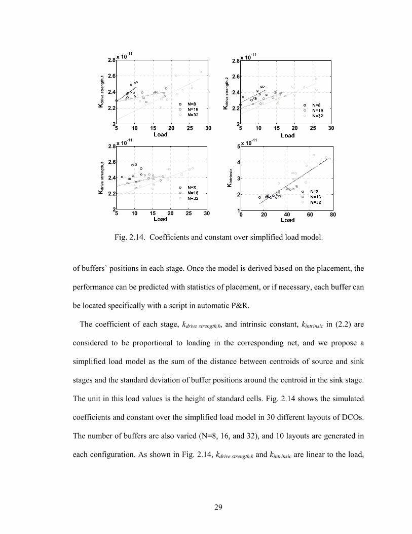
of buffers’ positions in each stage. Once the model is derived based on the placement, the
performance can be predicted with statistics of placement, or if necessary, each buffer can
be located specifically with a script in automatic P&R.
Fig. 2.14. Coefficients and constant over simplified load model.
5 10 15 20 25 302
2.2
2.4
2.6
2.8 x 10⁻¹¹
5 10 15 20 25 302
2.2
2.4
2.6
2.8x 10⁻¹¹
0 20 40 60 801
2
3
4
5x 10-11
5 10 15 20 25 302
2.2
2.4
2.6
2.8x 10⁻¹¹
Kdr
ive
stre
ngth
,1
Kdr
ive
stre
ngth
,2
Kdr
ive
stre
ngth
,3
Kin
trin
sic
The coefficient of each stage, kdrive strength,k, and intrinsic constant, kintrinsic in (2.2) are
considered to be proportional to loading in the corresponding net, and we propose a
simplified load model as the sum of the distance between centroids of source and sink
stages and the standard deviation of buffer positions around the centroid in the sink stage.
The unit in this load values is the height of standard cells. Fig. 2.14 shows the simulated
coefficients and constant over the simplified load model in 30 different layouts of DCOs.
The number of buffers are also varied (N=8, 16, and 32), and 10 layouts are generated in
each configuration. As shown in Fig. 2.14, kdrive strength,k and kintrinsic are linear to the load,
29

while kintrinsic has a higher dependency. Once the dependency is characterized in a process
technology, kdrive strength,k and kintrinsic are projected based on the placement of buffers.
Fig. 2.15. Minimum period over simplified load model.
10 20 30 40 50 60 70 800.8
0.9
1
1.1
1.2x 10⁻¹⁰
Min
imum
per
iod
The minimum period of each DCO is also predicted based on kdrive strength,k and kintrinsic.
From (2.2), the minimum period of a DCO is the sum of the coefficients and the constant,
and Fig. 2.15 shows the minimum period over the simplified load. The minimum period
shows a high dependency on the load, which is useful to project the minimum period
during the design phase.
Unlike kdrive strength,k and kintrinsic, the effective drive strengths are modeled based on the
distance between a pair of buffers from each source and sink stage, and analyzed in terms
of the interconnect delay. The Elmore delay model [39], which is the first moment of the
impulse response, has been pervasive for decades in synthesis and layout for modeling
interconnect delay. Though the Elmore delay can be written in a simple, closed form in
terms of design parameters such as device parasitics and the width of wires, it provides
limited accuracy. To improve the accuracy of the Elmore delay model, many variants
[40-42] also have been proposed. The computation of those models, however, is too
expensive for the cell-based DCO because it has an interconnect-intensive structure. Our
30

proposed timing model adopts another variant of the Elmore delay model, the Fitted
Elmore Delay (FED), since the FED improves accuracy while maintaining computing
efficiency [43]. In FED, the coefficients are determined by a curve fitting technique to
approximate Hspice simulation results. Following the FED, the interconnect delay can be
simplified as
· · . (2.5)
where a, b and c are determined by design parameters, and l is the wire length. Since the
design parameters are identical for the buffers and wires in the cell-based DCO, the values
of a, b, and c can be considered constant for each buffer. Also, the target model is the
normalized drive strength given in (2.3), thus only relative values of tint between buffers are
required. Then, (2.5) can be simplified as
· . (2.6)
(2.6) suggests that the interconnect delay can be approximated to be proportional to l2 as l
increases.
In the DCO, each stage has multiple buffers, and all buffers in consecutive stages are
connected to each other through a wire network. Thus, the timing models of a buffer should
be extended for the structure with multiple sources and multiple sinks. To derive an
interconnect model of the DCO, we propose a constant current source model as shown in
Fig. 2.16. Let tint (j, k) refer to an interconnect delay between source buffer j and sink buffer
k, and assume the output transition is linear. Then, the interconnect can be modeled as a
lumped capacitance driven by a constant current source, and the current value is as follows.
, ·· ,
(2.7)
31

where C is the lumped capacitance, and V is the supply voltage. Then, the constant current
source model can be extended to multiple sources (Fig. 2.17). When N source buffers drive
a sink k, the total curren fr h sink s obtai (2.8).
Fig. 2.16. Constant current source model for interconnect.
Fig. 2.17. Multiple current sources to a sink.
t om sources to t e i ned as
∑ , · ∑ , (2.8)
where ik is total current from source buffers to the sink k. Thus, the interconnect delay at
sink k by ik is as follows.
, ··
∑ , (2.9)
Since there are N buffers in the sink stage, the macro interconnect delay for a stage can be
expressed as a function of individual delays as (2.10). Assuming that tint,k’s have a small
32

standard deviation when all buffers are turned on, the function is approximated again as the
mean of the individual interconnect delays.
Fig. 2.18. Constant current source model.
, , … ,
, , , , … , , (2.10)
, , ,
The macro interconnect delay model in (2.9) and (2.10) indicates that the effect of each
buffer on the delay is different from each other, and the distribution can be approximately
modeled. Fig. 2.18 shows an example where one buffer in the source stage is turned off.
When turning off source 1, the current from sources to sink k is reduced by i(1,k), thus,
using (2.8) and (2.9), the in erco nect d y at the sink k is increased as follows. t n ela
, | ∑ , , (2.11)
Then, the incremental delay is
33

∆ , | , | ,
Fig. 2.19. Simplified wire length model.
,∑ , , ·∑ ,
, (2.12)
and the macro interconnect delay is increased as
∆ ∆ , | , … , ∆ , | . (2.13)
(2.13) corresponds to the incremental period in (2.4), thus the effective drive strength can
be represented as
,∆
∆ , . (2.14)
Through (2.6)-(2.14), dsk,i are calculated, and applied to (2.2). The wire length between a
pair of buffers, l in (2.6), however, is not available in the pre-layout model; thus
approximation of l is required. In the layout of standard cells, the length l between two
buffers can be approximated as the sum of the distance in X and Y coordinates (Fig. 2.19).
This approximation represents the minimum wire length between two buffers, while most
physical design algorithms seek minimum total wire length for non-critical signal paths
34

[44]. The validity of this approximation in modeling effective drive strength is verified in
Section 2.5.
Fig. 2.20. Comparison between effective drive strengths from measurement and model.
0 5 10 15 20 25 30 350.02
0.025
0.03
0.035
0.04
0.045
2.5. Experimental Results
In these experiments, effective drive strengths are calculated based on buffers’ positions,
then compared with the effective drive strengths calculated from measurements. Fig. 2.20
shows the effective drive strength from measurement and model in a stage of a DCO.
Though there are errors between the measurement and model, the model captures many of
the features due to P&R, considering the limited information used in the model. More
important than being able to predict each individual effective drive strength, however, is
the ability to predict the tuning range and resolution of a DCO using this model, as
discussed next.
The distribution of effective drive strengths plays an important role in the calibration
proposed in Section 2.3. In Fig. 2.7, the upper and lower limits of frequency control are
35

36
determined by turning off the buffers sorted in rising or falling order of effective drive
strength. Then, the frequency of the DCO can be controlled between the two lines by
reordering buffers to be disabled as shown in Fig. 2.7. Therefore, the shape of two lines
features the performance of the DCO. If the proposed model decently predicts the shape
with two lines, we can characterize the performance of the DCO. First, we sort the effective
drive strengths from measurement and model both in increasing and decreasing orders,
then plot cumulative sum of them in Fig. 2.21. The root mean square errors (RMSE)
between measurements and models are 0.0094, 0.0007, and 0.0017 on average for 10
different layouts of DCOs with N=8, 16, and 32, respectively.
Fig. 2.21. Cumulative sum of effective drive strength from measurement and model.
0 5 10 15 20 25 30 350
0.2
0.4
0.6
0.8
1
1.2
2.6. Summary
This chapter proposed a cell-based DCO to aid in an automated design procedure and
higher system integration with digital circuit blocks. The proposed DCO is composed of
tri-state buffers which are placed and routed by automatic design tools. The frequency of

the DCO is controlled by turning on a different number of buffers, and a calibration scheme
is proposed to achieve a high resolution frequency control. The timing model was derived
to address the P&R effect on the DCO performance. The proposed DCO is a core block in
the prototypes in Chapter 3 to Chapter 5.
37

Chapter 3
All-digital Synthesizable UWB Transmitter
3.1. Introduction
This chapter presents an all-digital impulse radio ultra-wideband (IR-UWB) transmitter
which is synthesized from a CMOS standard cell library, leveraging design automation
technologies. IR-UWB provides several characteristics favorable to all-digital transmitter
architectures. First, IR-UWB signaling is inherently duty-cycled. The width of UWB
pulses in the time domain is short (~2ns), while the pulse rate is relatively low. That is,
most of the time, the transmitter does not produce pulses. By implementing all-digital
architectures, the functional blocks can be turned off between pulses, thereby consuming
only leakage power. This significantly reduces power consumption in all-digital
transmitters. Second, IR-UWB is operated in non-coherent communication by applying
pulse position modulation (PPM) or on-off keying (OOK). Non-coherent communication
relaxes the frequency tolerance enough that typical accuracy specifications can be satisfied
by the time resolution of recent digital circuits. Recently published all-digital UWB
transmitters [18-21] take advantage of these characteristics to achieve low power and low
cost architectures. The proposed transmitter is not only implemented in an all-digital
architecture, but it is also implemented with standard cells in the automated design
procedure, adopting the cell-based DCO. Though standard cells are less flexible to
38

implement circuits with, the simulation, synthesis and layout of the cell-based circuits are
highly automated with current design tools. Since all functional blocks in the proposed
transmitter are implemented with standard cells and automatically place-and-routed, the
design procedure is significantly simplified, and a compact layout is derived. Also, by
adopting advanced CMOS technologies, the proposed transmitter achieves a low power
and small area, benefitting from process scaling.
The cell-based design of the transmitter, however, imposes several challenges, as
discussed in Chapter 2. Unlike custom layout, automated layout causes systematic
mismatch in the radio frequency signal paths. Also, since standard cells are minimally
sized, the cell-based circuits are relatively susceptible to process, voltage and temperature
(PVT) variations. To address these challenges, the transmitter provides a wide range of
center frequency and bandwidth of the UWB pulses which can be calibrated with high
resolution. With sufficient flexibility, the transmitter can compensate for the systematic
mismatch and variations, and it can target different applications. A calibration scheme
proposed in Section 2.3 is applied to address the systematic mismatch.
3.2. UWB Transmitter Architecture
A block diagram of the proposed UWB transmitter is shown in Fig. 3.1. According to
incoming data, a PPM modulator asserts a trigger edge in a modulated time slot, which
activates both a DCO and a delay line. When activated, the DCO begins oscillating at a
programmable frequency, and the DCO output is enabled. Simultaneously, the trigger
edge propagates through the programmable delay line. When the edge arrives at the end of
the delay line, the DCO output is disabled, forming a UWB pulse that takes the form of a
39

gated oscillator. The frequency of the DCO and the delay through the delay line are
digitally controlled by the frequency control word and pulse width control word,
respectively. In this way, the center frequency and bandwidth of UWB pulses are
separately controlled. The output of the delay line is also used to turn off the DCO to save
power between pulses, utilizing the duty-cycled nature of IR-UWB. The pulse start logic
detects the edge at the output of the delay line, and disables the DCO until the next trigger
edge is asserted. A scrambler is used to mimic delay-based binary phase shift keying
(DB-BPSK) [45] by randomizing the polarity of the pulses. In a PPM modulated spectrum,
UWB pulses have spectral lines, which limits the transmit power. With low hardware
complexity, the scrambler reduces the spectral lines, maximizing the transmit power within
the FCC mask.
Fig. 3.1. Block diagram of proposed UWB transmitter.
The transmitter provides a calibration mode where the center frequency and bandwidth
40

of the pulses are measured, and tuned for target performance. During the calibration mode,
the DCO is continuously enabled, and its frequency is measured by counting cycles over a
time period. A frequency divider, which is a chain of flip-flops, is inserted to reduce the
frequency of DCO output before the relatively slow counter. To calibrate the bandwidth of
the UWB pulses, the delay line is configured as a loop, and the frequency around the delay
line is measured with a similar technique. The counter values for the DCO and the delay
line indicate the current center frequency and the bandwidth of the UWB pulses, and the
digital control codes are adjusted according to target values.
Fig. 3.2. Digitally controlled oscillator embedding tunable delay cells.
3.2.1. Digitally Controlled Oscillator with Tunable Delay Cells
The core building block of the cell-based UWB transmitter is the cell-based DCO. Fig.
3.2 shows the structure of the DCO using the tunable delay cells. Each delay cell is
implemented with multiple inverting tri-state buffers connected in parallel. The first stage
includes a NAND gate and one less buffer to disable the DCO when necessary. According
to a target DCO performance, the number of buffers can be determined in the design phase.
The DCO in the transmitter was designed to have three stages to generate an oscillation
41

frequency ranging 3.1-to-5.0GHz, and each stage has 31 (in the first stage) or 32 buffers to
achieve sufficient resolution for non-coherent UWB communication. Instead of custom,
symmetric layout to achieve a desired performance, the buffers in the DCO are distributed
and routed by an automatic layout tool. This method significantly simplifies the design
procedure of the DCO, and enables a complete integration with other cell-based digital
blocks.
Fig. 3.3. Delay line embedding tunable delay cells.
3.2.2. Pulse Width Delay Line
Fig. 3.3 shows the structure of the delay line that employs tunable delay cells. A trigger
edge from the PPM modulator propagates through the delay line, and the edge at the output
of the delay line gates the DCO output to an antenna, thereby determining the width of the
UWB pulses. In the transmitter, the delay line has 57 tunable delay cells, and each delay
cell is implemented with 5 parallel tri-state buffers to cover a desired pulse width range.
Among the 57 stages in the delay line, the first 10 stages are used to block unavoidable
power supply transients when the DCO is turned on. To prevent this transient from
42

impacting the pulsed output, the gating logic turns on the DCO output only while the edge
in the delay line is propagating between stage 10 and stage 57. By controlling the delay in
the first 10 stages, we can control the time which the transmitter waits for the supply
voltage transients to settle. The pulse width of the UWB pulse is controlled with the
remaining 47 stages. Fig. 3.4 shows the measured pulse widths of the transmitter. When
every buffer is turned on in the 47 stages, the pulse width is shortest, and the pulse width is
increased by turning off the buffers. In the first section in Fig. 3.4, only one buffer is turned
off in each delay cell, and additional buffers are turned off for the next sections. Since the
delay cells have 5 buffers, there are four sections, whose values range from 1.1ns to 5.1ns.
Since the bandwidth of UWB pulses is required to be higher than 500MHz, the pulse width
should always be less than ~2ns; therefore, the fourth section is used only when the delay
line is significantly affected by PVT variations. The resolution of the pulse width control
varies (from 4ps to 47ps), based on the number of buffers off in each delay cell. A wide
range of pulse widths, calibrated with high resolution, is useful to compensate systematic
Fig. 3.4. Measured programmable pulse width range. By turning off tri-state buffers in the delay line, the pulse width is increasing.
0 10 20 30 40 50 601
2
3
4
5
6
43

mismatch and PVT variations, or target different applications. For instance, in a
multiple-channel communication, the pulse width is tuned to be wide, while the pulse
width is tuned to be short for single-channel communication.
Fig. 3.5. Delay-based BPSK scheme with scrambler.
LFSR
Scrambler
FromDCO
FromDelay line
1 or 0
Pulse widthwindow
LFSR=0
LFSR=1
3.2.3. Scrambler
PPM modulation has been popular in IR-UWB communication, offering reduced system
complexity over BPSK. Pulse generation in PPM modulation reduces power and area,
while BPSK requires functional blocks dissipating static power, and/or large passive
components. Also, PPM modulation allows non-coherent communication where receivers
also have low complexity and power efficiency. A spectrum in PPM modulation, however,
contains spectral lines which are 10log(PRF/1MHz) dB above the BPSK spectrum when
measured in a 1MHz bandwidth [46], where PRF is the pulse repetition frequency. Since
the power spectrum of UWB signaling is limited by the FCC mask, the maximum transmit
power in PPM modulation must be lowered by this factor.
In the proposed transmitter, a scrambler is used to reduce the spectral lines in the PPM
spectrum by randomizing the polarity of pulses. The scrambler consists of a linear
feedback shift register (LFSR) and an XOR gate. Between the pulses, the LFSR generates a
44

bit, which is 1 or 0, and the output of the DCO is XOR-ed with the LFSR bit. As shown in
Fig. 3.5, the output pulse is shifted by a half cycle when the LFSR bit is 1. When filtered by
an off-chip high-pass filter, the combined effect is equivalent to DB-BPSK [45], which is
transparent to a non-coherent receiver. Feedback taps in the LFSR are digitally
configurable, and a 16bit maximum length LFSR is configured in the transmitter.
3.3. Calibration of UWB Center Frequency
All functional blocks in the transmitter, including the DCO and the delay line, are
implemented with standard cells, and automatically place-and-routed. This cell-based
design methodology significantly simplifies the design procedure, and allows higher
system integration of the UWB transmitter. Though the characterization of the circuit
performance at the design phase becomes difficult due to systematic mismatch and
susceptibility to variations, the proposed DCO provides a wide range of frequencies which
are finely tunable with a digital calibration scheme. The proposed calibration scheme
proposed in Chapter 2 takes advantage of the systematic mismatch due to buffer placement
and wiring, which is represented as the effective drive strength.
Fig. 3.6 shows the measured incremental period for each buffer in stage 1 of the DCO.
Once the incremental periods for each buffer are measured, the buffers are sorted
according to their effective drive strengths (Fig. 3.7). If the buffers are turned off in order
beginning with the highest drive strength, the frequency decreases rapidly as shown by the
lower limit line in Fig. 3.8 (top). Turning off the buffers in order beginning with the
smallest drive strength decreases the frequency slowly, as shown by the upper limit line in
Fig. 3.8. These two controls determine the upper/lower limits of the DCO frequencies, and
45
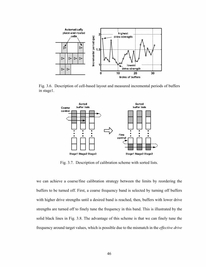
we can achieve a coarse/fine calibration strategy between the limits by reordering the
buffers to be turned off. First, a coarse frequency band is selected by turning off buffers
with higher drive strengths until a desired band is reached, then, buffers with lower drive
strengths are turned off to finely tune the frequency in this band. This is illustrated by the
solid black lines in Fig. 3.8. The advantage of this scheme is that we can finely tune the
frequency around target values, which is possible due to the mismatch in the effective drive
Fig. 3.6. Description of cell-based layout and measured incremental periods of buffers in stage1.
0 10 20 30
1
1.5
2
Fig. 3.7. Description of calibration scheme with sorted lists.
46

strength of each buffer. Also, the proposed calibration scheme guarantees monotonic
tuning of the frequency.
Fig. 3.8. Measured frequency control with sorted lists in DCO employing delay cells with 64 buffers, operating at 1V (top), and DCO employing delay cells with 32 buffers, operating at 0.9V (bottom).
0 10 20 30 40 50 60 700
1
2
3
4
5
6
7
0 20 40 60 80 100 120 140 160 180 2000
1
2
3
4
5
6
7
Freq
uenc
y (G
Hz)
Freq
uenc
y (G
Hz)
To study the impact of the number of buffers-per-stage on center frequency resolution,
we implemented two 3-stage DCOs, one with 32 buffers-per-stage, and one with 64. Fig.
3.8 shows the measured frequency control of these two DCOs. When 64 buffers are
embedded in each stage, and automatically place-and-routed, the incremental period of
each buffer is reduced, and the distribution of the incremental periods is widened. This
results in higher resolution, and clear coarse/fine tuning of the frequency as show in Fig.
3.8 (top). In the DCO with 32 buffers-per-stage, the incremental period is higher, and more
47

evenly balanced between buffers, which results in deteriorated resolution as shown in Fig.
3.8 (bottom). The measured frequency resolutions are 10MHz for the DCO with 64
buffers-per-stage, and 50MHz for the DCO with 32 buffers-per-stage. The IR-UWB
transmitter adopted the DCO with 32 buffers-per-stage because it provides a more compact
layout, lower power and higher maximum frequency. Furthermore, the 50MHz resolution
is adequate for non-coherent PPM [47], resulting in only 0.02dB loss when a
square-and-integrate receiver is used [17][48-50].
Fig. 3.9. Measured incremental period of buffers in stage 1 over 4 different chips.
0 5 10 15 20 25 30 350
0.5
1
1.5
2
The above coarse/fine calibration scheme requires a consistent order of the buffers’
incremental period over supply voltage and temperature variations, even though the
absolute value of incremental period may vary. In cell-based circuits, however, the relative
ordering of buffers’ drive strength is dominated by systematic mismatch due to routing. In
other words, the ordering of buffers depends mostly on the mismatched wiring, and the
order is not affected by other variables such as device mismatch, supply voltage or
temperature. To verify this, Fig. 3.9 shows the incremental periods of the buffers in stage 1
over four chips, and Fig. 3.10 shows the incremental periods over different supply voltages
48

and temperatures. Though the absolute values of the incremental period change, the order
of buffers in stage 1 is relatively consistent over the variations. Therefore, the order of the
buffers’ drive strengths are measured only once, after which they can be used to tune the
frequency regardless of voltage or temperature variation during the calibration mode. This
significantly simplifies the implementation of the calibration.
Fig. 3.10. Measured incremental period of buffers in stage 1 over different supply voltages (top, 0.85V, 0.9V, and 0.95V), and over different temperatures (bottom, -40°C, 25°C, and 80°C).
0 5 10 15 20 25 30 350
0.5
1
1.5
2
0 5 10 15 20 25 30 350
0.5
1
1.5
2
3.4. Measured UWB Transmitter Performance
The transmitter was fabricated in a 65nm CMOS process, and the micrograph and the
layout view of the transmitter are shown in Fig. 3.11. All functional blocks are integrated
49

through automatic place-and-route so that the transmitter occupies a small area. The area of
the transmitter is 0.032mm2. Benefitting from high operating frequency of 65nm standard
cells, the transmitter is operated at 0.9V (not at a nominal supply voltage, 1V), in order to
reduce power consumption. Fig. 3.12 shows the measured transient waveform of a 3.5GHz
UWB pulse. The output has a DC component that is characteristic of all-digital IR-UWB
Fig. 3.11. 65nm CMOS transmitter die micrograph and layout view.
Fig. 3.12. Measured transient waveform of UWB pulse at 3.5GHz after off-chip high-pass filter.
-2 -1 0 1 2 3 4-60
-40
-20
0
20
40
60
50

transmitters, since the transmitter generates UWB pulses that are switching between
supply voltage and ground. The DC spectrum is filtered by an off-chip high-pass filter. The
measured power spectral densities (PSD) when the transmitter is tuned to three channels
are shown in Fig. 3.13. The center frequency of the UWB pulse is tunable in the
3.1-to-5.0GHz frequency band with an average tuning step of 50MHz. The bandwidth of
Fig. 3.13. Measured output spectral densities of three channels after off-chip high-pass filter.
2 2.5 3 3.5 4 4.5 5 5.5-90
-80
-70
-60
-50
-40
PSD
(dB
m/M
Hz)
Fig. 3.14. Measured power spectral densities w/ and w/o scrambling. Without scrambling, PSD violates the FCC mask.
2 2.5 3 3.5 4 4.5 5-90
-80
-70
-60
-50
-40
51

the UWB pulse is also digitally controlled, and the measured bandwidth ranges from
500MHz to 1.4GHz. Fig. 3.14 illustrates the effect of DB-BPSK by the scrambler. When
the scrambler is enabled, the spectral lines, characteristic of PPM modulation, are
suppressed, allowing higher transmit power without violating the FCC mask.
Fig. 3.15. Measured output amplitude before/after filter of 13 chips. These are attenuated values (1dB) by cable in measurement.
0 2 4 6 8 10 12 1470
80
90
100
110
120
130
Consistent with the synthesized design, the final stage of the transmitter is a large,
standard cell inverter. The chips were packaged in a wirebonded 5mm x 5mm QFN
package, and an off-chip high-pass filter was used to attenuate the DC component of the
pulses. According to simulations, the inverter output can directly drive a 50Ω load with a
fixed amplitude of 84% of the supply voltage, when no losses from packaging and filtering
are considered. The pulse amplitude at the antenna will be reduced by packaging parasitics,
off-chip filter attenuation, and cable loss. Although package parasitics cannot be measured,
assuming an on-chip 20Ω trace resistance, 3nH bondwire inductance, and 3pF load
capacitance, the simulated attenuation of the pulse is 12.5dB. The measured off-chip filter
loss is 2.9dB from Fig. 3.15, and cable loss is 1dB. The sum of these losses account for the
52

limited amplitude reported in Fig. 3.12 and Fig. 3.15, and by utilizing better RF packaging
and antenna filtering, much higher radiated amplitudes are achievable.
Fig. 3.16. Measured temperature variation of center frequency control.
0 10 20 30 40 50 60 700
1
2
3
4
5
6
-40 -20 0 20 40 60 804
4.02
4.04
4.06
Fig. 3.15 also shows the variation of the output amplitude. The standard deviation of the
amplitude measured over 13 chips, including chip, package, and printed circuit board
(PCB), is 0.23dB. The maximum level of the transmitted PSD will depend on the pulse
amplitude and the pulse repetition frequency (PRF). Given the relatively constant
amplitude of output pulses, the transmitted PSD can be determined solely by the PRF.
Fig. 3.16 shows the measured variation of center frequency over a temperature range of
-40°C to 80°C. The frequency varies less than 2% over the temperature range, which is
well within the tuning range of the DCO. Fig. 3.17 shows the measured frequency control
and the maximum operating frequencies of 13 chips. The maximum frequency is limited
by the frequency divider in the transmitter, not by the DCO. All measured chips show
maximum frequency over 5GHz at 0.9V, satisfying the target performance. Though the
53
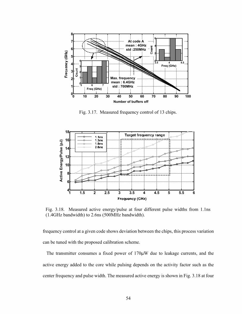
frequency control at a given code shows deviation between the chips, this process variation
can be tuned with the proposed calibration scheme.
Fig. 3.17. Measured frequency control of 13 chips.
0 10 20 30 40 50 60 70 80 90 1000
1
2
3
4
5
6
7
8
Number of buffers off
Max. frequencymean : 6.4GHzstd : 700MHz
At code Amean : 4GHz std :250MHz
Freq (GHz)3.5 4 4.50
2
4
6
5 6 70
1
2
3
4
Freq (GHz)
Fig. 3.18. Measured active energy/pulse at four different pulse widths from 1.1ns (1.4GHz bandwidth) to 2.6ns (500MHz bandwidth).
1 1.5 2 2.5 3 3.5 4 4.5 5 5.5 64
6
8
10
12
14
16
18
Act
ive
Ener
gy/P
ulse
(pJ)
The transmitter consumes a fixed power of 170μW due to leakage currents, and the
active energy added to the core while pulsing depends on the activity factor such as the
center frequency and pulse width. The measured active energy is shown in Fig. 3.18 at four
54
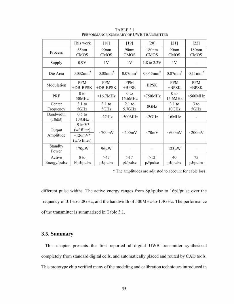
55
TABLE 3.1PERFORMANCE SUMMARY OF UWB TRANSMITTER
This work [18] [19] [20] [21] [22] 65nm
CMOS 90nm
CMOS 90nm
CMOS 180nm CMOS
90nm CMOS
180nm CMOS Process
Supply 0.9V 1V 1V 1.8 to 2.2V 1V -
0.032mm2 0.08mm2 0.07mm2 0.045mm2 0.07mm2 0.11mm2 Die Area
PPM PPM PPM PPM PPM BPSK Modulation +BPSK +BPSK +DB-BPSK +DB-BPSK +BPSK 0 to
15.6MHz 0 to
15.6MHz 0 to <560MHz<750MHz <16.7MHz PRF 50MHz
Center Frequency
3.1 to 3.1 to 2.1 to 5.7GHz 5GHz 5GHz 8GHz 3.1 to
10GHz 3 to
5GHz Bandwidth
(10dB) 0.5 to
1.4GHz ~2GHz ~500MHz ~2GHz 16MHz -
Output Amplitude
~91mV* (w/ filter) ~700mV ~200mV ~70mV ~600mV ~200mV ~126mV* (w/o filter)
Standby 170μW 96μW - - 123μW - Power Active
Energy/pulse 8 to
16pJ/pulse >47
pJ/pulse >17
pJ/pulse >12
pJ/pulse 40
pJ/pulse 75
pJ/pulse
* The amplitudes are adjusted to account for cable loss
different pulse widths. The active energy ranges from 8pJ/pulse to 16pJ/pulse over the
frequency of 3.1-to-5.0GHz, and the bandwidth of 500MHz-to-1.4GHz. The performance
of the transmitter is summarized in Table 3.1.
3.5. Summary
This chapter presents the first reported all-digital UWB transmitter synthesized
completely from standard digital cells, and automatically placed and routed by CAD tools.
This prototype chip verified many of the modeling and calibration techniques introduced in

Chapter 2 of this thesis for precisely regulating the frequency of a DCO and delay through
a delay line for controlling the center frequency and width of UWB pulses. In the following
chapters, I present components of an all-digital phase-locked loop synthesized from a
standard cell library that uses similar calibration techniques.
56

CHAPTER 4
All-Digital Synthesizable Time-to-digital Converter
4.1. Introduction
All-digital phase locked loop (ADPLL) is a recent active research area focused on
replacing conventional analog blocks in a PLL with an all-digital architecture, benefitting
from the performance of advanced digital processes [51][52]. Fig. 4.1 shows the general
block diagram of an ADPLL. In the ADPLL, a time-to-digital converter (TDC) compares
the phase error between the reference clock (Fref) and the divided clock (Fdiv). Then, the
digitized phase error is filtered by a digital loop filter (DLF), and utilized to control the
frequency of a digitally controlled oscillator (DCO). The TDC and DLF replace a charge
pump and large passive components of conventional analog PLLs, reducing the power
dissipation and area of the ADPLL. Also, the digital interface between the blocks enhances
testability and programmability of the ADPLL. In this architecture, the DLF and the
divider are required to satisfy only timing constraints; thus, they can be implemented with
digital logic circuits. On the other hand, the TDC and DCO directly affect the performance
of the ADPLL. Many structures for TDCs and DCOs have been proposed to achieve high
performance ADPLLs [53-59].
In this chapter, we focus on the TDC, and propose a cyclic Vernier structure which is
synthesized from a standard cell library. The quantization noise from the TDC, however,
57
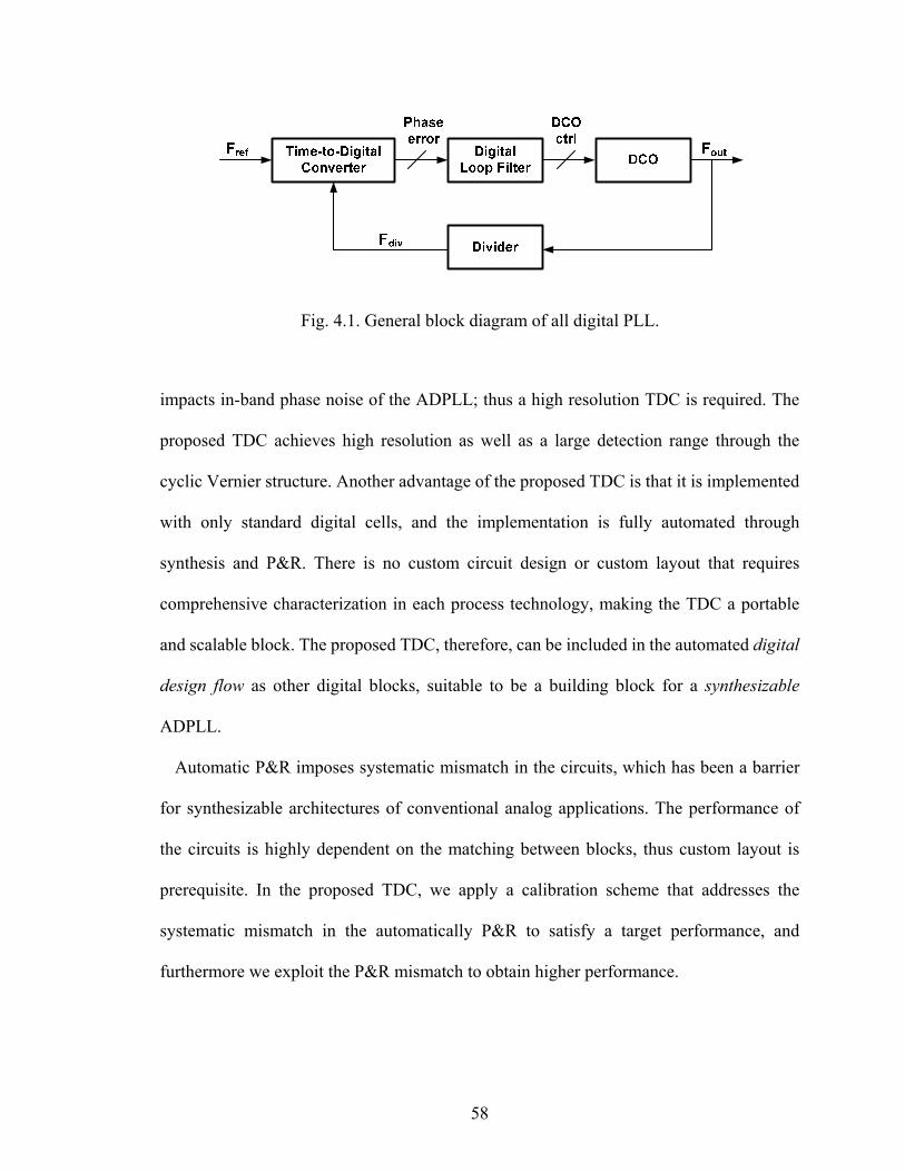
impacts in-band phase noise of the ADPLL; thus a high resolution TDC is required. The
proposed TDC achieves high resolution as well as a large detection range through the
cyclic Vernier structure. Another advantage of the proposed TDC is that it is implemented
with only standard digital cells, and the implementation is fully automated through
synthesis and P&R. There is no custom circuit design or custom layout that requires
comprehensive characterization in each process technology, making the TDC a portable
and scalable block. The proposed TDC, therefore, can be included in the automated digital
design flow as other digital blocks, suitable to be a building block for a synthesizable
ADPLL.
Fig. 4.1. General block diagram of all digital PLL.
Automatic P&R imposes systematic mismatch in the circuits, which has been a barrier
for synthesizable architectures of conventional analog applications. The performance of
the circuits is highly dependent on the matching between blocks, thus custom layout is
prerequisite. In the proposed TDC, we apply a calibration scheme that addresses the
systematic mismatch in the automatically P&R to satisfy a target performance, and
furthermore we exploit the P&R mismatch to obtain higher performance.
58

4.2. Cyclic Vernier Time-to-Digital Converter
4.2.1. TDC Architecture
Fig. 4.2 shows the block diagram of a cyclic Vernier TDC [53][54]. The goal of the TDC
is to measure the time difference between the rising edges of the ‘Start’ and ‘Stop’ signals,
which are Fref and Fdiv in the ADPLL, respectively. When the ‘Start’ is asserted, the slow
DCO starts to oscillate with a period of Ts, and the number of oscillations is counted by the
coarse counter. After an input delay of Tinput, the ‘Stop’ signal is asserted which triggers the
faster DCO to oscillate with a period of Tf. At this time, the coarse counter is disabled, and
the output of the counter represents a coarse measurement of the time between ‘Start’ and
(a)
(b)
Fig. 4.2. (a) Block diagram of the proposed TDC and (b) timing diagram.
Stop
Start
1
1
Ns
Nf
OSCs
OSCf
CNTs
CNTf
Tinput
Tcoarse Tfine
Detect
Detect
Ts
Tf
59

‘Stop’ rising-edges (Tcoarse). To improve the measurement accuracy, the residue of the
input delay (Tfine) is measured by the Vernier structure. When Tf is slightly smaller than Ts,
the time difference between rising edges of the two oscillations is reduced every cycle by
the difference in periods (Ts – Tf), and the edge of the fast DCO eventually catches up with
the slow DCO. By counting the number of cycles it takes for the fast DCO to catch up with
the slow DCO, Tfine is measured. Then, the overall measurement of Tinput can be determined
as follows.
(4.1)
(4.2)
where Ns and Nf are the number of cycles of the slow and fast oscillations, respectively,
and (Ts-Tf) is programmed to be much smaller than Ts. As shown in Fig. 4.2, the TDC
operates in two-steps; a coarse step and a fine step. The coarse step resolution is the period
of the slow DCO, and the fine step resolution is the difference between the periods of the
two DCOs. Note that the fine resolution does not depend on the absolute frequencies of the
DCOs, but only their difference in periods. This is crucial for the calibration of mismatch
between the P&R-ed DCOs discussed in Section 4.3.
Unlike conventional Vernier delay lines, the cyclic Vernier TDC adopts the ring
structure to extend input range, limited only by the counter size that easily scales according
to application. Also, the linearity of the TDC improves by utilizing the periods of the
DCOs, which is repetitive and consistent over operation, while the delay in Vernier delay
lines is more susceptible to variation and mismatch. The drawbacks of the cyclic Vernier
TDC are the accumulated jitter in ring oscillators, and a large latency of the fine step
measurement. It takes one period of the fast DCO cycle (Tf) to resolve a time difference of
60

one fine step resolution (Ts – Tf). To reduce the conversion time, we adopt the two-step
operation. The coarse step covers a large input time difference without any latency, and the
residue of the coarse step is measured by the fine step, which is less than one cycle of slow
DCO. Also, this fine step range can be further reduced by the edge detector described in
Section 4.2.3.
Fig. 4.3. Digitally controlled oscillator with tri-state buffers. The buffers from standard cell library are automatically placed-and-routed.
4.2.2. Digitally Controlled Oscillator
While the previous cyclic Vernier TDC architectures [53][54] adopt voltage controlled
oscillators (VCOs), which require custom design and layout, the proposed TDC adopts
DCOs that are implemented with standard cells. Fig. 4.3 shows the structure of the DCO.
The DCO consists of three stages, and each stage is implemented with eight parallel
inverting tri-state buffers which are digitally controlled. Tri-state buffers are available in
commercial standard cell libraries. While the load capacitance at each stage is fixed by the
number of buffers and wiring capacitance, the driving strength can be varied by turning on
a different number of tri-state buffers, thereby configuring the frequency of the DCO.
61

Since the buffers are automatically P&R-ed by design tools, the placement and routing of
the buffers are not regular as illustrated in Fig. 3, and it results in systematic mismatch in
the wiring capacitance, thus the effective drive strength of each buffer. Though the
individual drive strength cannot be controlled in the automated layout, the placement area
and the wire lengths are constrained by layout algorithms, and the distribution of the P&R
mismatch is predictable at the design phase.
In the proposed TDC, both the slow and fast DCOs are identically designed in the
Verilog description, and automatically P&R-ed. Then, the P&R mismatch is characterized
in the calibration mode, and the DCOs are configured to have slightly different periods,
utilizing the P&R mismatch. The P&R mismatch provides higher resolution for the TDC,
compared to the resolution obtained when the buffers are ideally matched. The calibration
scheme and measured results are shown in Section 4.3.
4.2.3. Edge Detector
Fig. 4.4 shows the structure of the edge detector which detects when the fast and slow
oscillator edges have aligned. At the frontend of the edge detector, a flip-flop detects the
phase of OSCs at the rising edge of OSCf. Since OSCf has a slightly smaller period, it
catches up with OSCs every cycle, and the output of the flip-flop switches when the two
Fig. 4.4. Structure of edge detector.
62

edges are in line. A flip flop from a standard cell library will have a finite setup time;
therefore, the detection event occurs when the OSCs edge is ahead of OSCf by the setup
time. This will appear as an offset in the TDC measurement, which would be digitally
corrected, or potentially even ignored, in a typical ADPLL application. Another issue with
the flip-flop is metastability. When the two edges are separated by the setup time, the delay
of the flip-flop increases and the output can be metastable; thus the phase of OSCs is not
detected in one cycle period. In the TDC, however, the OSCs and OSCf edges get closer by
the fine resolution every cycle, therefore if a metastable condition occurs, the output is
guaranteed to settle at the very next cycle.
Edge detection logic is included in the TDC to determine the direction of the phase shift
(low to high, or high to low), and terminate the fine step measurement early to save power.
When either edge is detected, the ‘Detect’ signal is asserted, and the ‘Edge’ signal indicates
the direction of the detected edge. When the rising edge of OSCs is detected, the ‘Edge’
signal is asserted, and the measured time indicates the fine step measurement (Tfine). On the
other hand, if the falling edge of OSCs is detected, ‘Edge’ is de-asserted, and half of Ts is
added to the measured time (Fig. 4.5).
While only one edge (rising edge) is detected in conventional TDCs, the proposed edge
detector detects rising and falling edges to save power consumption. Both DCOs are
oscillating during the fine measurement, and the power consumption is proportional to the
measurement time. By detecting either rising or falling edge, and terminating the fine step
measurement, the maximum measurement time is reduced by half, and the maximum
power consumption is reduced by as much.
63

4.3. TDC Calibration Utilizing Mismatch
A key challenge in the standard cell-based implementation is systematic mismatch
induced by automatic P&R, and addressing this mismatch is a primary focus of this thesis.
Unlike custom layout, automatic P&R generates significant mismatch in interconnects,
preventing accurate modeling of the analog performance. The systematic mismatch,
however, can be utilized for a higher resolution, if measured and calibrated accurately.
This section proposes a calibration scheme for the fine TDC resolution.
As shown in Fig. 4.3, there are a total of 23 tri-state buffers in each DCO (3 stages, 8
buffers / stage, and one NAND gate replacing a buffer in the first stage). Fig. 4.6 shows the
measured incremental period in stage 2 of the slow DCO. During a one-time calibration,
(a)
(b)
Fig. 4.5. Detection of (a) rising and (b) falling edges in the proposed phase detector.
64

the incremental periods of buffers are measured, and the buffers are sorted based on the
incremental period.
There are two resolutions in the proposed TDC, a coarse step resolution (Ts) and a fine
step resolution (Ts-Tf). First, the coarse step resolution is determined by configuring the
slow DCO. Fig. 4.7 shows the measured coarse step resolution, ranging from 170ps to
480ps. In Fig. 4.7, Ts is increased by turning off one additional buffer at each code in the
rotating order of stages. Although a DCO with three stages in 65nm CMOS can be faster,
the counters synthesized with standard cells cannot operate at the highest frequencies and
Fig. 4.6. Measured incremental period in stage 2 of slow DCO and sorted buffer list.
1 2 3 4 5 6 7 85.5
5.6
5.7
5.8
5.9
6
6.1
Incr
emen
tal p
erio
d (p
s)
cD
ecre
asin
g st
reng
th
Fig. 4.7. Measured coarse step resolution.
1 2 3 4 5 6 7 8 9 10100
200
300
400
500
Control code
65

become the limiting factor on operating frequency. The DCOs are, therefore, calibrated at
frequencies less than 6GHz, which is sufficient for many ADPLL applications.
The DCOs in the TDC are calibrated with a slightly different technique than described in
Chapter 3 for the UWB transmitter. When the coarse step resolution is determined, the fine
step resolution is obtained by configuring the fast DCO to have a slightly lower period. Fig.
4.8 shows the calibration scheme to utilize P&R mismatch. When the coarse step
resolution, for instance, is obtained by turning on three buffers in each stage, the calibration
starts with turning on the same number of buffers in the fast DCO. First, buffers on top of
Fig. 4.8. Description of fast DCO calibration.
stage1 stage2 stage3 stage1 stage2 stage3stage1 stage2 stage3
Sorted buffer lists in fast DCO
Afterstage1
Afterstage2,3
On Off
1
2
3
4
5
6
7
8
Fig. 4.9. Measured fine step resolution.
0 2 4 6 8 10 12 14 160
0.5
1
1.5
2
2.5
3
3.5
Fine
reso
lutio
n (p
s)
66

the sorted lists are enabled to have a lowest period. Then, the period is slightly increased by
swapping each buffer with a neighboring buffer in the list. Fig. 4.8 illustrates the
calibration process from the fastest DCO configuration to the slowest DCO configuration
when the number of enabled buffers per stage is maintained. The resulting range of period
(Tf) is around the coarse step resolution (Ts), and a desired fine step resolution (Ts – Tf) can
be obtained. Fig. 4.9 shows the measured fine step resolution, ranging from 0 to 3.3ps. If
P&R mismatch between two DCOs is excessive, and the whole range of Tf from the
Fig. 4.10. Measured fine step resolution variation over supply voltage (0.9V, 0.95V, 1V, 1.05V, and 1.1V).
0 2 4 6 8 10 12 14 16-1
0
1
2
3
4
5
Control code
0.90V0.95V1.00V1.05V1.10V
Fig. 4.11. Measured fine step resolution variation over temperature (0°C, 25°C, and 70°C).
0 2 4 6 8 10 12 14 16-1
0
1
2
3
4
Control code
0°C25°C70°C
67

calibration is not around Ts, the TDC resolution can be tuned by turning off a different
number of buffers in each DCO. Ultimately, the performance of the TDC is determined by
the fine step resolution. For the ADPLL application, we are therefore mainly interested in
the calibration of the difference between two periods, and less on their absolute values.
Fig. 4.10 and Fig. 4.11 show the measured fine step resolution over supply voltage and
temperature variation. Although the environmental variation significantly affects the
absolute value of the periods, Ts and Tf, we focus on the difference between periods which
determines the fine resolution of the TDC. When configuring the fine resolution as 1ps at
nominal condition, both supply voltage (0.9V) and temperature (70°C) variation increases
the resolution up to 1.5ps. In the ADPLL application, the variation affects the stability of
ADPLL, which is a function of many parameters such as DLF and DCO gain. Thus, the
stability of the ADPLL can be addressed with other ADPLL parameters, considering the
environmental variations.
4.4. TDC Performance
The proposed cyclic Vernier TDC was fabricated in 65nm CMOS, and the micrograph
and layout view of the TDC is shown in Fig. 4.12. All functional blocks are integrated
through automatic P&R so that the TDC occupies a small area. The core area of the TDC is
only 0.006mm2.
The input time difference (Tinput) in the following measurements is generated by a
Tektronix AWG5012 arbitrary waveform generator with a step size of 1ps. To eliminate
input jitter from the waveform generator and the measurement setup, each value is
obtained by averaging 1000 measurements in Fig. 4.13 and Fig. 4.15. Also, nonlinearity of
68

the generated delay from the AWG5012 is adjusted, and applied in the figures.
Fig. 4.12. Micrograph and layout view of TDC.
80 µm
80 µm
TDC core
4.4.1. TDC measurement
Fig. 4.13 shows the TDC measurement with the two-step operation. The slow DCO is
tuned to have a period of 220ps by turning off the buffers. Then, the period of the fast DCO
is calibrated to have a slightly lower period as described in Section 4.3. Fig. 4.13 shows
two different fine step resolutions, 1ps and 5ps. According to the target performance, the
coarse and fine step resolutions are digitally reconfigured, providing flexibility to the TDC.
Fig. 14(a) shows the single shot measurements of the TDC. Assuming the application of
ADPLLs, the TDC is required to operate with high accuracy when the ADPLL is in lock, or
close to locking. Thus, the single shot measurements are shown for the input range where
the coarse code is zero. The measured standard deviation of the fine codes ranges from
2.7ps to 4.3ps when the fine resolution is set as 5.5ps. Thus the maximum standard
deviation of the single shot measurements is 0.78 LSB.
69

Fig. 4.13. Coarse and fine measurement of TDC.
2.1 2.12 2.14 2.16 2.18 2.215
20
25
30
35
2.1 2.12 2.14 2.16 2.18 2.20
30
60
90
120
150
0 0.5 1 1.5 2 2.5 3 3.5 4 4.50
5
10
15
20
Fig. 14(a) shows that the jitter of the DCO affects the TDC measurement, and the
standard deviation of the fine code increases as the time difference increases. Fig. 14(b)
and Fig. 14(c) show the standard deviation of the measurements over a large range of input
time differences, and the standard deviation over the sum of the coarse and fine codes.
From these figures, the standard deviation can be modeled as a function of the sum of
coarse/fine cod wes, hich fits (4.3).
0.044 2.35 (4.3)
Eq. (3) indicates that the TDC precision is affected by the measurement range. Assuming
an ADPLL application with a reference frequency of 10MHz, the maximum range is 100ns
which is covered by the ring structure and the on-chip counters. Though the measured
standard deviation at 100ns is 23ps, the precision improves as the ADPLL moves closer to
being locked, and the TDC operates with a precision of 0.78LSB when the ADPLL is
locked.
70

Fig. 4.14. (a) Single shot measurements over constant inputs with a fine resolution of 5.5ps, (b) standard deviation over a large range of inputs, and (c) standard deviation over sum of coarse/fine codes.
0 20 40 60 80 100 1202
4
6
8
0 5 10 152
4
6
8
35 40 45 50 550
1000
2000
3000
4000
5000
6000
20 25 30 35 400
1000
2000
3000
4000
5000
6000
5 10 15 20 250
1000
2000
3000
4000
5000
6000
4.4.2. Rising/falling Edge Detection and TDC in ADPLL
To reduce the conversion time in the fine step, we proposed an edge detector that detects
both rising and falling edges. Fig. 4.15 shows the measured fine codes when this scheme is
applied. As shown in Fig. 4.15, when the fine step range is over about a half cycle of OSCs,
71

the edge detector starts to detect falling edges, rather than rising edges. In this way, the
maximum conversion time of the fine step can be reduced by half.
Fig. 4.15. Measurement time reduction by detecting either of rising or falling edge.
2.1 2.15 2.2 2.250
10
20
30
40
50
60
Input time difference (ns)
Falling edge detection
Rising edge detection
Fig. 4.16. Calculated output vs. input time difference. In this figure, the offset from input signal paths such as cable and PCB is adjusted. The measured duty cycle is 41%, and the deviation by duty cycle variation is observed.
2 2.1 2.2 2.3 2.4
2
2.1
2.2
2.3
2.4
The proposed detection scheme, however, causes inaccuracy in the measurement due to
duty cycle variation. Fig. 4.16 shows the calculated TDC output from the coarse output
code and fine output code. As can be seen in this figure, the calculated output from falling
edge detection deviates from the desired values, if the duty cycle varies. Fig. 4.16 also
shows inaccuracy around multiple cycles of OSCs due to coarse/fine code ratio mismatch.
72

Fig. 4.17. Application of TDC in ADPLL.
Time-to-DigitalConverter
DigitalLoop Filter DCO
Fref Fout
Fdiv
Phase error
DCOctrl
Targetoffset
To Divider
The application of the proposed TDC, however, is a phase detector in ADPLLs for clock
synthesis. If the PLL is programmed to be locked close to zero phase error, the phase error
greater than a half cycle of OSCs is used to steer the ADPLL dynamics, and the
performance is dependent only on the lower phase error measurements when the ADPLL is
locked. The measured DNL and INL are less than 1 LSB when the phase error is lower than
a half cycle of OSCs. Though the inaccuracy of the duty cycle affects the pre-lock
operation of the ADPLL, it is not critical for the purpose of the ADPLL when locked.
In the ADPLL application, a target offset value can be subtracted from the TDC output
before it is filtered by DLF as shown in Fig. 4.17. The purpose of the target offset is to lock
the ADPLL while the TDC output is non-zero. When the TDC output is close to zero, it is
possible that cycle slipping could occur, depending on the ADPLL implementation.
Subtracting a target offset value also increases the time difference between ‘Start’ and
‘Stop’ in the TDC measurement when the ADPLL is in lock, thereby increasing the power
consumption. By locking to a positive target offset, the TDC output is maintained around
the offset value, and cycle slipping in the ADPLL can be avoided.
If a target offset, α, is set, the real phase error between two edges are considered to be
(setup time + transient offset + α), where the transient offset is defined as an offset
73

originated from transient cycles when the DCOs start to oscillate. Though the absolute
phase is less critical in the proposed application of clock generation, it is required to be
consistent during operation. Environmental variations such as supply voltage and
temperature can cause variation in the phase error during operation, which needs to be
addressed. If the setup time varies, the phase detection point is varied, generating an offset.
In a simulation of the D flip-flop, the setup time varied by as much as 0.8ps over -40°C to
80°C, and it varied by as much as 2.1ps over 0.9V to 1.1V (10% variation). Another source
of offset in the TDC is transient offset due to transient cycles of the DCOs while starting to
oscillate. During this startup time, the period of the DCOs may deviate from the
steady-state period values. Simulations show that the transient offset of the TDC is around
0.5 periods, and it varies by as much as 0.06 periods and 0.08 periods with temperature and
supply voltage variation, respectively.
4.4.3. Power
The power dissipation in the Vernier structure depends on Tinput, and the sampling
frequency of the TDC. The DCOs, which are the most power hungry blocks in the TDC,
oscillate only when Tinput is measured. Therefore, the TDC operation is duty-cycled, and
power dissipation is proportional to the sampling frequency.
During the coarse step operation, only the slow DCO oscillates, and the measurement
time is the same as the Tcoarse without any latency. During the fine step operation, however,
both DCOs are oscillating, and the measurement time is inversely proportional to the fine
step resolution, and multiplied by Ts. The measured power consumption during coarse and
fine step measurements is as follows.
74

75
TABLE 4.1PERFORMANCE SUMMARY OF TDC
This work [54] [55] [56] [57] [58]
65nm 130nm 90nm 130nm 90nm 65nm Process CMOS CMOS CMOS CMOS CMOS CMOS
Supply 1.0V 1.5V 1.0V 1.5V 1.2V 1.2V
0.006mm2 0.263mm2 0.6mm2 0.04 mm2 0.02mm2 0.02mm2 Die Area
Cyclic Vernier
Gated Passive 2D Technique Cyclic Vernier Time amp. Ring osc. Interp. Vernier
T (4.4) 1.4 F
2.6 Tf F (4.5)
where Pcoarse and Pfine is power during coarse and fine step, and Fs is sampling frequency of
the TDC. The performance of the TDC is summarized in Table 4.1.
4.5. Summary
This chapter presents a prototype TDC designed for all-digital PLLs. The main
advantage of this TDC over other presented work is the synthesis from a standard cell
library using automatic P&R tools. In this case, it resulted in a TDC much smaller and
Resolution 5.5ps 2ps (sim) 1.25ps 6ps 0.6/1.2 4.8ps 8ps (meas)
Single shot precision
0.008 LSB x (coarse+fine) +0.42 LSB
< 1 LSB 0.64 LSB - 0.7 LSB -
Measurement range 15 bits* 12 bits 9 bits 11 bits 7 bits 7 bits
Power
Max. 1.4mW (coarse)
Max. 0.63mW (fine)
7.5mW 3mW 3.3mW – 31.5mW 3.6mW 1.7mW
Sampling frequency 10MHz 15MHz 10MHz 50MHz 180MHz 50MHz
* The precision varies over the range. The range is 11 bits for a precision less than 1 LSB.

lower power than other TDCs presented, without much loss in resolution. In the next
Chapter, a complete ADPLL is presented using this TDC architecture.
76

Chapter 5
Synthesizable ADPLL
In this chapter, we present measurement results of a synthesized ADPLL. The ADPLL is
implemented with the proposed DCO and TDC; thus all functional blocks are synthesized
from a standard cell library. Though ADPLL is currently a very active research area, this is
the first ADPLL fully implemented with standard cells, following the automatic design
flow. The ADPLL can be applied to clock generation of digital systems, and portability of
the proposed ADPLL to other designs and processes is useful for fast turnaround of digital
systems.
5.1. Introduction
Recently published all-digital phase locked loops (ADPLL) have shown several
advantages over conventional analog PLLs, in terms of area, scalability, testability, and
programmability [27-31]. This section presents an ADPLL suitable for clock synthesis for
digital systems such as microprocessors. All functional blocks in the ADPLL are designed
with digital standard cells, synthesized from a commercial cell library, and automatically
placed and routed (P&R) using design tools. The design procedure of this completely
synthesizable ADPLL significantly shortens the design time compared to custom circuit
77

design and layout, and it enhances portability of the ADPLL as a building block for various
applications. Automatic P&R introduces variation in the placement and routing of cells in
the ADPLL. This is particularly a challenge in the design of precision blocks such as the
digitally controlled oscillator (DCO) and time-to-digital converter (TDC). A calibration
scheme is presented that accounts for systematic mismatch from automatic layout of the
DCO, which is also applied to the DCO-based TDC. The calibration for the DCO in this
ADPLL differs from calibration schemes presented in prior chapters in that this calibration
operates in a closed-loop controller. This means the state of the DCO buffers must be
maintained and ordering taken into account when the controller issues commands to speed
up or slow down the DCO frequency. For this reason, a local SRAM is implemented with
the ADPLL.
5.2. ADPLL Architecture
A block diagram of the proposed ADPLL is shown in Fig. 5.1. The TDC compares the
edges of the reference clock (Fref) and the divided output clock (Fdiv), and provides 16-bit
phase difference measurements to the digital loop filter (DLF). The proposed TDC
operates in two steps; a coarse step and a fine step, producing 8 MSBs and 8 LSBs,
respectively. The prescaler combines this output by weighting the MSBs and the LSBs
separately, making a 16-bit input to the DLF. This enables floating point processing of the
TDC output, and provides more programmability of the coarse/fine step resolutions. The
DLF consists of a proportional path and an integral path, each with programmable
coefficients. The 3-bit MSBs of the DLF output determine whether the DCO controller
increases, decreases, or holds the DCO frequency. The 8-bit LSBs of the DLF output are
78

used to dither the DCO frequency to reduce the effect of limit cycles. The dithering block is
clocked at a higher frequency of Fout /4. Finally, Fout is divided by an integer N (1-to-511),
and compared with Fref. In calibration mode, on-chip counters are used for one-time
characterization of the TDC and the DCO, which is later used to control them in locking
mode.
Fig. 5.1. Block diagram of proposed ADPLL.
5.3. Circuit Implementation
5.3.1. DCO and DCO Controller
All blocks, including the DCO, are constructed only of standard cells and synthesized
from a commercial cell library. Fig. 5.2 shows the block diagram of the DCO and control
blocks. The DCO consists of 5 stages, and each stage is implemented with 64 inverting
tri-state buffers connected in parallel (63 buffers in Stage1). The maximum frequency is
obtained when all buffers are turned on, and the frequency is reduced by turning off buffers.
79

Instead of custom layout to achieve matched delays [29-31], the buffers in the DCO are
P&R’ed by design tools. Similar to the DCOs in the UWB transmitter and TDC, this
introduces systematic mismatch between buffer delays that is dominated by routing
variation. In calibration mode, the effective drive strength of each buffer is measured,
capturing the relative differences between buffers. Buffers are sorted based on drive
strength, and the reordered indexes are stored in a local memory. The DCO controller
decodes one row of the memory each cycle, and turns on/off the indexed buffers according
to the DLF output. This reordering procedure provides a coarse/fine frequency control, and
improves the resolution of the DCO. Two buffers in Stage2 and Stage3 are dedicated to
dither the DCO frequency. The dithering block generates 2-bit control signals to
pseudo-randomly turn on/off the buffers at a rate proportional to the 8 LSBs of the DLF
output.
Fig. 5.2. Block diagram of DCO and control blocks.
Stage 1 Stage 2 Stage 3
Start / Stop
64 buffers/stage
Stage 4 Stage 5
DCOController
63 63+1 63+1 64 64
x64
Dithering
DCO
317
30
6
addr
2
Mem
data
3
8stage1 stage2 stage3 stage4 stage5
Buffer index
80

Fig. 5.3. Calibration algorithm utilizing systematic mismatch.
0 20 40 60 80 1001.8
2
2.2
2.4
2.6
2.8
3
Freq
uenc
y (G
Hz)
0 10 20 30 40 50 600
0.5
1
1.5
Incr
emen
tal p
erio
d (p
s)
Fig. 5.3 illustrates the DCO control scheme to address systematic mismatch caused by
automatic P&R. When all buffers are enabled, the DCO oscillates at its maximum
frequency. If only one buffer is turned off, the DCO period slightly increases. We refer to
this as the incremental period for that buffer, implying an effective drive strength of each
buffer. The measured incremental periods for the 62 buffers in Stage1 of the DCO are
shown in Fig. 5.3. The buffers in each stage are reordered based on the incremental periods
and stored in the memory while in calibration mode. When the ADPLL is in locking mode,
the DCO controller turns off the buffers following the order stored in memory. During
coarse control, 5 buffers at a time are turned off from the top of the memory, which has the
highest drive strengths. During fine control, only one buffer is turned off from the bottom
of the memory, which has the lowest drive strengths. The coarse control range is
81

programmable by the starting memory address, which enables fast-locking at a target
frequency range. The fine control achieves higher resolution by turning off buffers with the
lowest drive strength. The measured fine-frequency resolution is 3MHz/step at 2.5GHz.
Fig. 5.4. Measured DCO frequency control over (a) voltage, (b) temperature, and (c) process variation.
2.8 2.85 2.9 2.950
0.5
1
1.5
2
0 50 100 150 200 250 3000
1
2
3
4
0 50 100 150 200 250 3000
1
2
3
4
Freq
uenc
y (G
Hz)
Freq
uenc
y (G
Hz)
Cou
nt
This coarse/fine frequency control is obtained due to systematic mismatch by automatic
P&R. If the buffers and wiring were completely matched, the incremental periods of the
buffers would all be the same, and a coarse/fine tuning would not be possible. Instead, the
frequency would be determined only by the absolute number of enabled buffers, regardless
of which ones were used. The proposed calibration scheme therefore leverages the
systematic wiring mismatch by reordering buffers to achieve better resolution at desired
coarse frequency bands.
To address the sensitivity of the synthesized ADPLL over environmental variations, the
DCO frequency control is measured over PVT variation as shown in Fig. 5.4. The DCO
82

frequency varies less than 10% and 15% over the voltage and temperature variation,
respectively. The maximum DCO frequencies of 5 chips are also measured to address
process variation. The mean of the maximum frequency is 2.9GHz with a standard
deviation is 37.4MHz. The above PVT variation is within a few coarse control steps in the
proposed calibration scheme, and can be overcome by the broad DCO frequency range and
its programmability when the ADPLL operates in closed-loop.
Fig. 5.5. Measured incremental period of buffers in Stage1 over (a) voltage, (b) temperature, and (c) process variation.
0 10 20 30 40 50 600
0.5
1
1.5
0 10 20 30 40 50 600
0.5
1
1.5
Index of buffers
Index of buffers
1.10V1.05V1.15V
25°C-40°C80°C
(a)
(b)
The proposed calibration scheme requires a consistent order of the buffers over supply
voltage and temperature variations, since the index of buffers is reordered and stored in the
memory while in calibration mode, and remains during the ADPLL locking mode. Since
the systematic mismatch is dominant in the automatically P&R-ed DCO, the order of the
buffers’ drive strengths is relatively consistent over environmental variations as shown in
Fig. 5.5 by the same relative shapes of the incremental periods, resulting in the same sorted
83
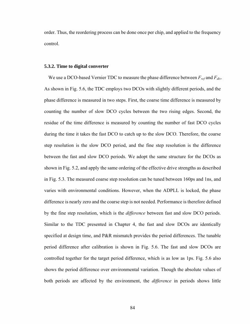
order. Thus, the reordering process can be done once per chip, and applied to the frequency
control.
5.3.2. Time to digital converter
We use a DCO-based Vernier TDC to measure the phase difference between Fref and Fdiv.
As shown in Fig. 5.6, the TDC employs two DCOs with slightly different periods, and the
phase difference is measured in two steps. First, the coarse time difference is measured by
counting the number of slow DCO cycles between the two rising edges. Second, the
residue of the time difference is measured by counting the number of fast DCO cycles
during the time it takes the fast DCO to catch up to the slow DCO. Therefore, the coarse
step resolution is the slow DCO period, and the fine step resolution is the difference
between the fast and slow DCO periods. We adopt the same structure for the DCOs as
shown in Fig. 5.2, and apply the same ordering of the effective drive strengths as described
in Fig. 5.3. The measured coarse step resolution can be tuned between 160ps and 1ns, and
varies with environmental conditions. However, when the ADPLL is locked, the phase
difference is nearly zero and the coarse step is not needed. Performance is therefore defined
by the fine step resolution, which is the difference between fast and slow DCO periods.
Similar to the TDC presented in Chapter 4, the fast and slow DCOs are identically
specified at design time, and P&R mismatch provides the period differences. The tunable
period difference after calibration is shown in Fig. 5.6. The fast and slow DCOs are
controlled together for the target period difference, which is as low as 1ps. Fig. 5.6 also
shows the period difference over environmental variation. Though the absolute values of
both periods are affected by the environment, the difference in periods shows little
84

variation. Calibration of the TDC is therefore needed once to account for the systematic
mismatch.
Fig. 5.6. Block diagram of TDC and fine step resolution control.
1 2 3 4 5 6 7 8-4
-2
0
2
4
1 2 3 4 5 6 7 8-4
-2
0
2
4
5.3.3. Prescaler
In the two-step measurement of the TDC, the coarse step resolution is the period of the
slow DCO, and the fine step resolution is the difference between two periods of the fast and
slow DCOs; thus, the units of the coarse and fine counter values are the coarse step
resolution and the fine step resolution, respectively. To concatenate 8 bits from each
counter to form the input to the following DLF, the coarse step resolution is required to be
28 times the fine step resolution.
85

Fig. 5.7. Description of prescaler operation.
Fig. 5.7 shows the operation of the prescaler, which helps match the units of coarse and
fine measurements. According to programmable control codes, the coarse counter output
and the fine counter output are shifted, and concatenated. This is also useful for flexible
PLL performance. Depending on the resolution requirements of the ADPLL, the fine
resolution is programmed, and the fine counter output is shifted accordingly, without
re-calibrating the coarse step resolution.
5.3.4. Digital loop filter
Fig. 5.8 shows the model of the DLF, which is a programmable digital filter with a
proportional path and integral path. The proportional coefficient (KP) and integral
coefficient (KI) are programmed according to the desired performance of the ADPLL, and
the coefficients are chosen to be power of two; thus the internal values are shifted rather
than multiplied. The input to the DLF is the 16-bit scaled TDC output, and the output of the
DLF is internally 16-bits. The DCO control scheme, however, turns on or off one buffer at
a time, and therefore does not require all 16 bits. Thus, 11 bits of the filter output are wired
86

to the DCO controller. The 3 MSB bits of the DLF output are used by the DCO controller
to determine whether to turn on or off buffers to increase or decrease the frequency, and the
8 LSB bits of the DLF output are passed to the dithering block, which finely controls the
DCO frequency.
Fig. 5.8. z-domain model of Digital loop filter (DLF).
Fig. 5.9. Structure of counter-based divider.
5.3.5. Divider
The divider in the ADPLL is counter-based (Fig. 5.9), and the integer-N divide value is
programmable from 1 to 511. Since the input signal has a relatively high frequency of over
2GHz, the first two bits of the internal counter are structurally described in Verilog with an
87

inverting D-flip flop chain, and later bits are counted by a synthesized counter. The
following divider logic outputs an oscillating signal with a divided frequency.
Fig. 5.10. Linear model of ADPLL.
5.3.6. Linear model of ADPLL
A linear model of the overall ADPLL is required to obtain the loop dynamics of the
system and predict the phase noise at the output. First, a simplified linear model of each
functional block is obtained, and the overall loop transfer function, G(s), is calculated. Fig.
5.10 shows the linear model of the overall system. In the TDC, the phase information is
converted to time, and the time is digitized. Thus, the gain of the TDC is expressed as
follows.
GainTDCT
·∆TDC (5.1)
where T is the reference period, and ∆TDC is the fine resolution of the TDC.
The DLF can also be expressed as a linear block with a transfer function, H(z). Since the
DLF is a discrete-time functional block, H(z) is expressed in z-domain that is obtained
from Fig. 5.8.
88

H z KPKI (5.2)
The proposed DCO controller turns on or off only one buffer at a time, which is not linear
operation. However, the dithering process increases or decreases the frequency
proportional to the output of the DLF when the ADPLL is in lock, which approximates the
DCO control as a linear block. Since the phase is obtained by integrating the frequency of
the DCO, the overall gain of the DCO is expressed as (5.3) in the s-domain.
GainDCO·KDCO (5.3)
The divider divides the phase by N, and discrete/continuous time domain conversion is
expressed with T and 1/T.
Combining the above linear models of the components in the system, we can obtain an
open loop gain, A(s).
A s T∆· TDC
· H s · ·KDCO ·N
(5.4)
H s H z | T/T/
(5.5)
where the transfer function of the DLF is transformed to the s-domain through the
bilinear transformation. Then, a closed loop transfer function, G(s), is derived from
(5.6).
G s AA
(5.6)
From (5.6), the closed loop bandwidth of the overall system is around 1MHz, which is one
tenth of the reference frequency.
Fig. 5.11 shows the linear model of the overall ADPLL with noise sources. Various noise
sources can be simplified as two primary sources, which are the TDC quantization noise (tq)
89
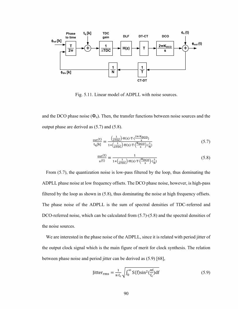
and the DCO phase noise (Φn). Then, the transfer functions between noise sources and the
output phase are derived as (5.7) and (5.8).
Fig. 5.11. Linear model of ADPLL with noise sources.
T2π
1∆TDC H(z) T 2πKDCO
s
1N
1T
+ +
Phase to time
TDCgain DLF DT-CT DCO
CT-DT
ref [k]
div [k]
out (t)
tq [k] n (t)
∆TDC ·H ·T· ·KDCO
∆TDC ·H ·T· KDCO · N
(5.7)
∆TDC ·H ·T· KDCO · N
(5.8)
From (5.7), the quantization noise is low-pass filtered by the loop, thus dominating the
ADPLL phase noise at low frequency offsets. The DCO phase noise, however, is high-pass
filtered by the loop as shown in (5.8), thus dominating the noise at high frequency offsets.
The phase noise of the ADPLL is the sum of spectral densities of TDC-referred and
DCO-referred noise, which can be calculated from (5.7)-(5.8) and the spectral densities of
the noise sources.
We are interested in the phase noise of the ADPLL, since it is related with period jitter of
the output clock signal which is the main figure of merit for clock synthesis. The relation
between phase noise and period jitter can be derived as (5.9) [68],
Jitter·
S f sin df (5.9)
90

where fc is the center frequency, and L(f) is the phase noise of the ADPLL. The jitter in the
clock signal from the ADPLL is a function of the phase noise in the spectrum, which can be
addressed with noise sources in the TDC and the DCO, and design parameters in the closed
loop transfer function, G(s).
Fig. 5.12. Measured output clock signal and jitter histogram at 2.5GHz (top) and power consumption of ADPLL (bottom).
1.6 1.8 2 2.2 2.4 2.69
10
11
12
13
14
15
-20 -10 0 10 200
1
2
3
4
5
6x 10⁴
5.4. Measurement Results
The ADPLL was fabricated in 65nm CMOS. The active area of the ADPLL is
185x190μm2, and the memory occupies an additional 85x90μm2. The ADPLL operates at
1.1V, and the output frequency locks from 1.5GHz to 2.7GHz. Fig. 5.12 shows the period
jitter, and power consumption of the ADPLL. At 2.5GHz, the RMS and peak-to-peak jitter
91

92
is 3.2psrms and 36pspp, respectively. The ADPLL dissipates 4.6mW/GHz over the
frequency range with an offset of 2.2mW. The chip micrograph of the ADPLL is shown in
Fig. 5.13, and the performance is summarized in Table 5.1.
Fig. 5.13. Die micrograph of ADPLL.
5.5. Summary
This is the first reported ADPLL to be designed completely from standard logic cell and
automatically placed and routed by CAD tools. While the performance is comparable to
other recently reported ADPLLs, the main advantage of this synthesized ADPLL is the
design cycle time is much shorter when compared to other ADPLLs with custom design
and layout.

TABLE 5.1PERFORMANCE SUMMARY OF ADPLL
This work [27] [28] [29] Process 65nm CMOS 65nm CMOS 65nm CMOS 65nm CMOS technology
0.042mm2 0.045mm2 0.027mm2 0.048mm2 Area
Supply Voltage 1.1V 1.3V / 1.1V 1.1-1.3V 1.2V
13.7mW 11.6mW 19.7mW Power - @ 2.5GHz @ 3GHz @ 2GHz
Output frequency 1.5 to 2.9GHz 0.19 to 4.27GHz 600 to 800MHz 1 to 2GHz
3.6psrms 1.4psrms 21psrms 1.0psrms @ 2.5GHz @ 3GHz @ 800MHz @ 2GHz
Jitter 46pspp 15pspp 193pspp 16.6pspp
@ 2.5GHz @ 3GHz @ 800MHz @ 2GHz
93

Chapter 6
Conclusions
With the introduction of nanometer-scale CMOS technologies, all-digital architectures
have been proposed to take advantage of digital circuits, while analog circuits suffer from
reduced supply voltage and increased noise. All-digital architectures, however, still depend
on custom circuits and layouts, which do not fully utilize advanced design automation
common in digital designs. To incorporate all-digital architectures in the automated design
flow, a cell-based design methodology was proposed. In this design procedure, circuits are
described in hardware description languages such as Verilog, then, synthesized and
P&R-ed by automatic design tools; thereby providing higher integration, portability, and
scalability. Also, standard cell engineering provides building blocks for the circuits in
advanced process technologies, where the cells only benefit from process scaling.
This work covered several aspects of cell-based design for synthesizable analog/RF
applications. First, the cell-based design requires structural modification, which enables
synthesizable circuits. A core block, a cell-based DCO is proposed. Implemented with
tri-state buffers connected in parallel, the DCO is P&R-ed by automatic design tools. The
cell-based DCO can be applied to many applications such as transmitters and PLLs,
replacing custom oscillators. Since oscillators are core blocks in analog/RF circuits, the
cell-based DCO can be an important milestone for synthesizable analog/RF circuits.
94

95
While automatic P&R increases productivity of cell-based designs, it also imposes
systematic mismatch that cannot be characterized with conventional verification methods.
To address the effect of P&R, a concept of effective drive strength was proposed, and
applied to the timing model and calibration scheme. The proposed timing model based on
effective drive strength captures the effect of P&R in the parallel structures, and the
distribution of effective drive strength was approximated with only placement information
with low error. This model can be applied in two ways; first, the placement of buffers can
be specified to achieve a target performance, which can be done easily with script for
design tools. Second, the placement of buffers by P&R can be statistically modeled. Then,
the distribution of effective drive strength, thereby the performance of cell-based DCO,
can be also statistically modeled.
Finally, the proposed calibration scheme provided a monotonic frequency control with
improved resolution. Since the number of configurations of the DCO increases
exponentially with the number of buffers, frequency control becomes complicated as the
size of the DCO grows. By sorting the buffers and storing them in a memory, the frequency
control is dramatically simplified. Though it requires additional functionality for sorting
and storing buffer control signals, the systematic mismatch is dominated by layout which is
consistent over process, voltage, and temperature variation. Thus, the initial calibration
may be done only once per design, reducing manufacturing cost.
The feasibility of the proposed cell-based circuits for analog/RF application was verified
through prototypes, an IR-UWB transmitter, a TDC, and an ADPLL. The proposed
structures, timing model, and calibration schemes allowed these all-digital architectures to
be synthesizable, and the measurements of the prototypes showed comparable

performance as well as advantages of the cell-based designs. The prototypes, however, also
point out design challenges which are required to be addressed in the future. First, standard
cells are single-ended; thus, the circuits are susceptible to supply noise. To reduce the
supply noise, sensitive circuit blocks require a separate supply domain, or differential cell
structures need to be proposed. Also, the signal from the cell-based design includes a DC
component, which requires an off-chip filter for RF applications. Second, the proposed
design requires calibration structures such as an embedded memory and on-chip counter,
and additional manufacturing process for calibration. Though the relative cost of additional
circuitry decreases as process scales, some applications still require minimal designs which
are advantageous in terms of area and power consumption. Finally, the proposed
calibration scheme can also be affected by reduced supply voltage. As shown in Chapter 2,
it is possible that random effects become more apparent as supply voltage scales. To
maintain the dominance of systematic mismatch, which is useful to simplify the calibration,
the buffers are required to be distributed sparsely during P&R, trading off area and power.
With efforts in structural study, modeling, and calibration to address the above design
challenges, the proposed cell-based design becomes more promising in the advance
process technologies.
96

Bibliography
[1] A-J. Annema, B. Nauta, R. van Langevelde, and H. Tuinhout, “Analog Circuits in
Ultra-Deep-Submicron CMOS,” IEEE J. Solid-State Circuits, vol. 40, pp. 132-143, Jan. 2005.
[2] L. L. Lewyn, T. Ytterdal, C. Wulff, and K. Martin, “Analog Circuit Design in Nanometer-scale CMOS Technologies”, IEEE Proceedings of, vol. 97, pp. 1687-1714, 2009.
[3] P. R. Kinget, “Designing analog and RF circuits for ultra-low supply voltages,” IEEE European Solid State Circuits Conference, pp. 58-67, 2007.
[4] B. Murmann, P. Nikaeen, D. J. Connelly, and R. W. Dutton, “Impact of Scaling on Analog Performance and Associated Modeling Needs,” IEEE Trans. on Electron Devices, vol. 53, .no. 9, Sep. 2006.
[5] B. Murmann, “A/D Converter Trends: Power Dissipation, Scaling and Digitally Assisted Arhitectures,” IEEE Custom Integrated Circuits Conf., pp. 105-112, Sep. 2008.
[6] B. Murmann, “Digitally-assited analog circuits,” IEEE Micro, vol. 26, no. 2, pp. 38-47, Mar.-Apr. 2006.
[7] R. H. M. van Veldhoven et al., “An Inverter-Based Hybrid ∑∆ Modulator,” IEEE Int. Solid-State Circuits Conf., pp. 493-494, Feb. 2008.
[8] C. Donovan and M. Flynn, “A ‘Digital’ 6-bit ADC in 0.25-um CMOS,” IEEE J. Solid State circuits, vol. 37, pp. 432-437, Mar. 2002.
[9] S. Park, et al., “A 40GS/s 5-b Flash ADC in 0.18um CMOS,” IEEE J. Solid-State Circuits, vol .42, no. 9 pp. 1865-1872, Sep. 2007.
[10] B. P. Ginsburg and A. P. Chandrakasan, “Highly Interleaved 5b 250MS/s ADC with Redundant Channels in 65nm CMOS,” Int. Solid-State Circuits Conf. Dig. Tech. Papers, pp. 240-241, Feb. 2008.
[11] W. Namgoon, “ A channelized digital ultrawadeband receiver,” IEEE Trans. Wireless Communications, pp. 502-510, Mar. 2003.
97

[12] Y. Oh and B. Murmann, “A Low-Power, 6-bit Time-Interleaved SAR ADC Using OFDM Pilot Tone Calibration,” IEEE Custom Integrated Circuits Conf., pp. 193-196, Sep. 2007.
[13] S. Chung and J. L. Dawson, “A 73.1dB SNDR digitally assisted subsampler for RF power amplifier linearization systems,” IEEE VLSI circuits, Symposium on, pp. 148-149, Jun. 2009.
[14] H. H. Boo, S. W. Chung, and J. L. Dawson, “Adpative Predistortion Using a ∆∑ Modulator for Automatic Inversion of Power Ammplifier Nonliearity,” IEEE Trans. on Circuits and Systems-II, vol. 56, no. 12, Dec. 2009.
[15] M. Teplechuk, T. Gribben, and C. Amadi, “Filterless integrated Class-D Adio Amplifier Achieving 0.0012% THD+N and 96dB PSRR When Supplying 1.2W,” IEEE Int. Solid-State Circuits Conf., Feb. 2011.
[16] M. Pastre and M. Kayal, “Digital Calibration Methodology Applied to a Sensor Microsystem,” IEEE int. Conf. on Automation, Quality and Testing, Probotics, pp. 110-113, Dec. 2006.
[17] F. Lee and A. Chandrakasan, “A 2.5 nJ/b 0.65 V 3-to-5 GHz subbanded UWB receiver in 90nm CMOS,” IEEE Int. Solid-State Circuits Conf. Dig. Tech. Papers, pp. 116-117, Feb. 2007.
[18] D.D. Wentzloff, and A. P. Chandrakasan, “A 47pJ/pulse 3.1 to 5GHz all-digital UWB transmitter in 90 nm CMOS,” IEEE Int. Solid-State Circuits Conf. Dig. Tech. Papers, pp. 118-119, Feb., 2007.
[19] J. Ryckaert, et al., “A 0.65-to-1.4nJ/burst 3-to-10GHz UWB Digital TX in 90nm CMOS for IEEE 802.15.4a,” IEEE Int. Solid-State Circuits Conf., Dig. Tech. Papers, Feb. 2007.
[20] V.V. Kulkarni, M. Muqsith, K. Niitsu, H. Ishikuro, and T. Kuroda, “A 750 Mb/s, 12pJ/b, 6-to-10GHz CMOS IR-UWB Transmitter with Embedded On-Chip Antenna,” IEEE J. Solid-State Circuits, vol. 44, pp. 394-403, Feb. 2009.
[21] P.P. Mercier, D.C. Daly, and A.P. Chandrakasan, “An Energy-Efficient All-Digital UWB Transmitter Employing Dual Capacitively-Coupled Pulse-Shaping Drivers,” IEEE J. Solid-State Circuits, vol. 44, pp. 1679-1688, June 2009.
[22] A. P. Chandrakasan et al., “Low-Power Impulse UWB Architectures and Circuits,” IEEE Proc. of, vol. 97, no. 2, Feb. 2009.
[23] T. Norimatsu et al., “A UWB-IR transmitter with digitally controlled pulse generator,” IEEE J. Solid-State Circuits, vol. 42, pp. 1300-1309, Jun. 2007.
98

[24] H. Kim, D. Park, and Y. Joo, “All-digital low-power CMOS pulse generator for UWB system,” Electron, Lett., vol. 40, no. 24, pp. 1523-1535, Nov. 2004.
[25] IEEE 802.15.4a Wireless MAC and PHY Specifications for LR-WPANs, IEEE Std. 802.15.4a, 2007.
[26] R. B. Staszewski, C-M. Hung, N. Barton, M-C. Lee, and D. Leipold, “A Digitally Controlled Oscillator in a 90nm Digital CMOS Process for Mobile Phones,” IEEE J. Solid-State Circuits, vol. 40, no. 11, pp. 2203-2211, Nov. 2005.
[27] W. Grollitsch, R. Nonis, and N.D. Dalt, “A 1.4psrms-Period-Jitter TDC-Less Fractional-N Digital PLL with Digitally Controlled Ring Oscillator in 65nm CMOS,” ISSCC Dig. Tech. Papers, pp. 478-479, Feb. 2010.
[28] M.S-W. Chen, D. Su, and S. Mehta, “A Calibration-Free 800MHz Fractional-N Digital PLL with Embedded TDC,” ISSCC Dig. Tech. Papers, pp. 472-473, Feb. 2010.
[29] A.V. Rylyakov, J.A. Tierno, D.Z. Turker, J-O. Plouchart, H.A. Ainspan, and D. Friedman, “A Modular All-Digital PLL architecture Enabling Both 1-to-2GHz and 24-to-32GHz Operation in 65nm CMOS,” ISSCC Dig. Tech. Papers, pp. 516-517, Feb. 2008.
[30] J.A. Tierno, A.V. Rylyakov, and D. Friedman, “A Wide Power Supply Range, Wide Tuning Range, All Static CMOS All Digital PLL in 65 nm SOI,” IEEE J. Solid-State Circuits, vol. 43, no. 1, pp. 42-51, Jan. 2008.
[31] T. Olsson and P. Nilsson, “A Digitally Controlled PLL for SoC Application,” IEEE J. Solid-State Circuits, vol. 39, pp. 751-760, May. 2004.
[32] M. Zanuso, S. Levantino, C. Samori, and A. Lacaita, “A 3MHz-BW 3.6GHz Digital Franctional-N PLL with Sub-Gate-Delay TDC, Phase-Interpolation Divider, and Digital Mismatch Cancellation,” IEEE Int. Solid-State Circuits Conf. Dig. Tech. Papers, pp. 476-477, Feb., 2010.
[33] J. Borremans, K. Vengattaramane, V. Giannini, and Jan. Craninckx, “A 86MHz-to-12GHz Digitally-Intensive Phase-Modulated Fractional-N PLL Using a 15pJ/Shot 5ps TDC in 40nm digital CMOS,” IEEE Int. Solid-State Circuits Conf. Dig. Tech. Papers, pp. 480-481, Feb., 2010.
[34] S. Lee, Y. Seo, Y. Suh, H. Park, J. Sim, “A 1GHz ADPLL with a 1.25ps Minimum-Resolution Sub-Exponent TDC in 0.18um CMOS,” IEEE Int. Solid-State Circuits Conf. Dig. Tech. Papers, pp. 482-483, Feb., 2010.
[35] R. B. Staszewski, et al., “All-Digital PLL and Transmitter for Mobile Phones,” IEEE Journal of Solid State Circuits, vol. 40, no. 12, pp. 2469-2482, Dec. 2005.
99

[36] C. Hsu, M. Z. Straayer, and M. H. Perrott, “A Low-Noise Wide-BW 3.6-GHz Digital ∆∑ Fractional-N Frequency Synthesizer With a Noise-Shaping Time-to-Digital Converter and Quantization Noise Cancellation,” IEEE Journal of Solid State Circuits, vol. 43, no. 12, pp. 2776-2786, Dec. 2008.
[37] M. Lee, M. E. Heidari and A. A. Abidi, “A Low Noise, Wideband Digital Phase-locked Loop based on a New Time-to-Digital Converter with Subpicosecond Resolution,” IEEE Symposium on VLSI Circuits Dig. pp. 112-113, Jun. 2008.
[38] V. Kheterpal et al., “Design methodology for IC manufacturability based on regular logic-bricks,” in Proc. ACM/IEEE Design Automation Conf., pp. 353-358, June 2005.
[39] W. C. Elmore, “The transient response of damped linear network with particular regard to wideband amplifiers,” Journal of Applied Physics, 1948.E. Barajas, D. Gomez, D. Mateo, and J. L. Gonzalez, “A 75pJ/bit All-Digital Quadrature Coherent IR-UWB Transceiver in 0.18µm CMOS,” IEEE Radio Frequency Integrated Circuits Symposium, pp. 197-200, May 2010.
[40] B. Tutuianu, F. Dartu, and L. Pileggi, “An explicit RC-circuit delay approximation based on the first three moments of the impulse response,” IEEE/ACM Design Automation Conference, pp. 463-368, 1998.
[41] A. B. Kahng and S. Muddu, “Two-pole analysis of Interconnection trees,” IEEE Multi-Ship Module Conference, pp. 105-110, Jan. 1995.
[42] A. B. Kahng and S. Muddu, “An analytical delay model for RLC interconnects,” IEEE Int. Symposium on Circuits and Systems, pp. 4237-4240, May 1996.
[43] A. I. Abou-Seido, B. Nowak, and C. Chu, “Fitted Elmore Delay: A Simple and Accurate Interconnect Delay Model,” IEEE Int. Conf. on Computer Design, pp.422-427, 2002.
[44] K. D. Boese, A. B. Kahng, B. A. McCoy, and G. Robins, “Rectilinear Steiner Trees with Minimum Elmore Delay,” IEEE Design Automation Conf. pp. 371-386, 1994.
[45] D. D. Wentzloff, A. P. Chandrakasan, "Delay-Based BPSK for Pulsed-UWB Communication," IEEE International Conference on Speech, Acoustics, and Signal Processing, pp. 561-564, Apr. 2007.
[46] Y. Nakache and A. Molisch, “Spectral shaping of UWB signals for time hopping impulse radio,” IEEE Journal on Selected Areas in Communications, vol. 24, no. 4, pp. 738-744, Apr. 2006.
[47] J. Qian, S.Pullela, and Lawrence Pillage, “Modeling the “Effecitve Capacitance” for the RC Interconnect of CMOS Gates,” IEEE Tans. on Computer-Aided Design of Integrated Circuits and Systems, vol. 13, no. 12, Dec. 1994.
100

101
[48] T. A. Pahn, V. Krizhanovskii, and S. G. Lee, “Low-power CMOS energy detection transceiver for UWB impulse radio system,” IEEE Custom Integrated Circuits Conf., pp. 675-678, Sep. 2007.
[49] Y. Zheng, Y. Tong, J. Yan, Y. P. Xu, W. G. Yeoh, and F. Lin, “A low power noncoherent CMOS UWB transceiver ICs,” IEEE Radio Freq. Integrated Circuits Symp., pp. 347-350, Jun. 2005.
[50] L. Stoica, S. Tiuraniemi, I. Oppermann, and H. Repo, “An ultra wideband low complexity circuit transceiver architecture for sensor networks,” IEEE Int. Symp. Circuits System, vol. 1, pp. 364-467, May 2005.
[51] M. Lee, M. E. Heidari, and A. A. Abidi, “A Low Noise, Wideband Digital Phase-locked Loop based on a New Time-to-Digital Converter with Subpicosecond Resolution,” IEEE VLSI Symp. Dig. Tech. Papers, pp. 112-113, Jun. 2008.
[52] M.S-W. Chen, D. Su, and S. Mehta, “A Calibration-Free 800MHz Fractional-N Digital PLL with Embedded TDC,” ISSCC Dig. Tech. Papers, pp. 472-473, Feb. 2010.
[53] P. Chen, C. C. Chen, J. C. Zheng, and Y. S. Shen, “A PVT Insensitive Vernier-Based Time-to-Digital Converter With Extended Input Range and High Accuracy,” IEEE Trans. on Nuclear Science, vol. 54, pp. 294-302, Apr. 2007.
[54] J. Yu, F. F. Dai, and R. C. Jaeger, “A 12-Bit Vernier Ring Time-to-Digital Converter in 0.13µm CMOS Technology,” IEEE J. Solid-State Circuits, vol. 45, no. 4, pp. 830-842, April 2010.
[55] M. Lee, and A. A. Abidi, “A 9b, 1.25 ps Resolution Coarse-Fine Time-to-Digital Converter in 90nm CMOS that Amplifies a Time Residue,” IEEE J. Solid-State Circuits, vol. 43, no. 4, pp. 769-777, April 2008.
[56] M. Z. Straayer, and M. H. Perrott, “A Multi-Path Gated Ring Oscillator TDC With First-Order Noise Shaping,” IEEE J. Solid-State Circuits, vol. 44, no. 4, pp. 1089-1098, Apr. 2009.
[57] S. Henzler, S. Koeppe, W. Kamp, H. Mulatz, and D. Schmitt-Landsiedel, “90nm 4.7ps-Resolution 0.7-LSB Single-Shot Precision and 19pJ-per Shot Local Passive Interpolation Time-to-Digital Converter with On-Cihp Characterization,” IEEE Int. Solid-State Circuits Conf. Dig. Tech. Papers, Feb. 2008.
[58] L. Vercesi, A. Liscidini, and R. Castello, “Two-Dimensions Vernier Time-to-Digital Converter,” IEEE J. Solid-State Circuits, vol. 45, no. 8, pp. 1504-1512, August 2010.
[59] A. Mantyniemi, T. Rahkonen, and J. Kostamovaara, “A CMOS Time-to-Digital Converter (TDC) Based On a Cyclic Time Domain Successive Approximation

102
Interpolation Method,” IEEE J. Solid-State Circuits, vol. 44, no. 11, pp. 3067-3077, November 2009.
[60] E. Iroaga and B. Murmann, “A 12b, 75MS/s Pipelined ADC Using Incomplete Settling,” IEEE J. Solid-State Circuits, vol. 42, no. 4, pp. 748-756, Apr. 2007.
[61] D. H. Kwon, H. Li, Y. Chang, R. Tseng, and Y. Chiu, “Digitally Equalized CMOS Transmitter Front-End With Integrated Power Amplifier,” IEEE J. Solid-State Circuits, vol. 45, no. 8, Aug. 2010.
[62] J. Kim, Y.Woo, J. Moon, and B. Kim, “A new wideband adaptive digital predistortion technique employing feedback linearization,” IEEETrans. Microw. Theory Tech., vol. 56, no. 2, pp. 385–392, Feb. 2008.
[63] M. Thian, M. Xiao, and P. Gardner, “Digital baseband predistortion based linearized broadband inverse Class-E power amplifier,” IEEE Trans. Microw. Theory Tech., vol. 57, no. 2, pp. 323–328, Feb. 2009.
[64] J. Yuan, H. Y. Chan, S. W. Fung, and B. Liu, “An Activity-Triggered 95.3 dB DR 75.6 dB THD CMOS Imaging Sensor With Digital Calibration,” IEEE J. Solid-State Circuits, vol. 44, no. 10, pp. 2834-2843, 2009.
[65] A. D. Berny, A. M. Niknjad, and R. G. Meyer, “A 1.8-GHz LC VCO With 1.3-GHz Tuning Range and Digital Amplitude Calibraion,” IEEE J. Solid-State Circuits, vol. 40, no. 4, Apr. 2005.
[66] R. L. Kirlin, “An All-Digital Second-Order PLL,” IEEE Trans. on Aerospace and Electronic Systems, pp. 710-712, 1974.
[67] C-F. Liang, S-H. Chen, and S-I. Liu, “A Digital Calibration Technique for Charge Pumps in Phase-Locked Systems,” IEEE J. Solid-State Circuits, vol. 43, no. 2, Feb. 2008.
[68] A. A. Abidi, “Phase Noise and Jitter in CMOS Ring Oscillators,” IEEE J. Solid-State Circuits, vol. 41, no. 8, Aug. 2006.