a carbon nanotube-based hundred watt-level ka-band
TRANSCRIPT
This article has been accepted for inclusion in a future issue of this journal. Content is final as presented, with the exception of pagination.
IEEE TRANSACTIONS ON ELECTRON DEVICES 1
A Carbon Nanotube-Based Hundred Watt-LevelKa-Band Backward Wave Oscillator
Xuesong Yuan , Qingyun Chen, Xiaotao Xu, Matthew T. Cole , Senior Member, IEEE,Yu Zhang , Zexiang Chen, and Yang Yan
Abstract— Carbon nanotube (CNT) cold-cathodes holdmuch promise in a variety of millimeter-wave and terahertzvacuum electronic radiation devices due to their inherentnear instantaneous temporal turn-on and near-ideal idealfield electron emission performance. Here we report on thedevelopment of a CNT cold-cathode Ka-band backward-wave oscillator (BWO). Using a novel beam compressionstage, theoretical studies, simulation results, and empiricalfindings collectively demonstrate that this device affords anunprecedentedly high output power of 230 W at a techno-logically important operating frequency of 33.65 GHz. Thedeveloped magnetic injection electron gun achieves a highemission current of 265.5 mA (emission current densityof 188.3 mA/cm2) and a high focused beam current densityof 18.5 A/cm2, which our studies suggest, is essential to theBWOs high output power.
Index Terms— Backward wave oscillator (BWO), carbonnanotube (CNT), cold cathode, field emission (FE), highpower, millimeter-wave (MMW) radiation.
I. INTRODUCTION
OWING to their high output power and high operatingfrequency, vacuum electronic radiation sources (VERS)
have been deployed widely in many technologies, includ-ing radar, biology, imaging, and communications [1]–[4].At present, commercially available VERS typically utilizeconventional thermionic cathode electron guns that are bulky
Manuscript received January 21, 2021; revised March 3, 2021;accepted March 10, 2021. This work was supported in part by theNational Key Research and Development Program of China under Grant2019YFA0210202, in part by the National Natural Science Foundationof China under Grant 61771096, in part by the Sichuan Science andTechnology Program under Grant 2021YJ0096, and in part by theFundamental Research Funds for the Central Universities under GrantZYGX2019J012. The review of this article was arranged by EditorR. Letizia. (Xuesong Yuan and Qingyun Chen are co-first authors.)(Corresponding author: Xuesong Yuan.)
Xuesong Yuan, Qingyun Chen, Xiaotao Xu, and Yang Yan are with theSchool of Electronic Science and Engineering, University of ElectronicScience and Technology of China, Chengdu 610054, China (e-mail:[email protected]; [email protected]).
Matthew T. Cole is with the Department of Electronic andElectrical Engineering, University of Bath, Bath BA2 7AY, U.K. (e-mail:[email protected]).
Yu Zhang is with the State Key Laboratory Optoelectronic Materialsand Technologies, Sun Yat-sen University, Guangzhou 510275, China(e-mail: [email protected]).
Zexiang Chen is with the School of Optoelectronic Science andEngineering, University of Electronic Science and Technology of China,Chengdu 610054, China (e-mail: [email protected]).
Color versions of one or more figures in this article are available athttps://doi.org/10.1109/TED.2021.3066144.
Digital Object Identifier 10.1109/TED.2021.3066144
and require additional heater driver electronics. Thermionicsources are inherently functionally limited due to theirhigh-temperature operation and comparatively slow temporalresponse [5], [6]. Electron emission from thermionic cathodesrequires comparatively lengthy preheating and thermalizationtimes, which are often tens to hundreds of seconds. Though notparticularly problematic during operation, the removal of addi-tional heating circuitry from the electron sources helps driveimportant mass and volume reduction—a system-level designpriority in many VERS applications. Perhaps the most pressingchallenge facing thermionic-based devices is the ongoingdifficulty in source miniaturization. As a result, research onthe development of millimeter-wave (MMW) VERS has beenlargely stifled due to the lack of suitable emission sourceswhich to develop new VERS on.
Though much-hyped, functional assessment of field emis-sion (FE) cold cathode material continues to highlight themas the leading alternative for the replacement of incum-bent thermionic electron sources in MMW VERS [7], [8].Nanostructured cold cathodes have come to the fore in thevacuum electronics community due to their engineered sur-face properties and nanoscale morphologies, which allow forroom temperature operation [9], self-ballasting emission [10],low turn-on voltages [11], and time stable electron emis-sion [12]–[14]. The near-instantaneous switch-ON time [15]of such nanostructured FE sources removes the need for anypreheating or thermal conditioning of the electron emitter.Nanostructured FE sources have long lifetimes [14], andfacile system architectures [16], [17] are inexpensive to inte-grate due to their design simplicity, all of which allow foraggressive volume and mass miniaturization [17]–[22]. Withinthe absence of surface-bound adsorbents, carbon nanotubes(CNTs) emitters afford significantly extended operation timescompared to other electron source technologies [14]. Thoughthe emergence of a wide variety of new 1-D and 2-D materialshas stimulated a revival in electron emission-based research,due to their comparative maturity CNTs remain one of themost attractive materials upon which to develop electronemission devices [23]. Their high electronic and thermalconductivity, large aspect ratio, and excellent chemical andmechanical stability continue to drive significant on-goingresearch efforts [23]–[26]. To date, several attempts have beenmade to increase the FE current from CNT cold-cathodes andintegrate them into VERS devices to support the developmentof new technologies [21], [24], [26]. Previously, we havedesigned a truncated-cone CNT cold-cathode electron gun
0018-9383 © 2021 IEEE. Personal use is permitted, but republication/redistribution requires IEEE permission.See https://www.ieee.org/publications/rights/index.html for more information.
Authorized licensed use limited to: UNIVERSITY OF BATH. Downloaded on March 30,2021 at 09:51:54 UTC from IEEE Xplore. Restrictions apply.
This article has been accepted for inclusion in a future issue of this journal. Content is final as presented, with the exception of pagination.2 IEEE TRANSACTIONS ON ELECTRON DEVICES
with beam transmission of nearly 100% and a maximumemission current of 100 mA [16]. This electron gun wassuccessfully used to develop a fully sealed 0.22-THz-gyrotronwith an output power of 500 mW [27]. These systems demon-strate viable integration pathways toward the development of anew generation of functionally advanced nanomaterial-basedcold-cathode VERS. Nevertheless, the output power of thisgyrotron remained limited to only a few hundred milliwatts,making it unsuitable for many applications which requireorders of magnitude higher output powers [26]. This work wasextended by Li et al. [28] who used our truncated-cone CNTcold-cathode as a reference device when they developed amagnetic-focused X-band traveling wave tube (TWT) capableof delivering an emission current of 358 μA at 12.5 kV/mm.Unfortunately, the CNT cathode was damaged during pulsedmode testing, and the output power of their TWT was notextensively characterized or reported [28]. To date, princi-pally due to the comparatively low emission current densityachieved, there has been very little progress in producing highpower MMW and terahertz VERS based on CNT cold cathodethat is capable of operating at hundreds of watts [29]–[33].This report looks to address this.
Capable of generating microwaves up to the THz frequencyrange, one of the most established VERS devices is thebackward-wave oscillator (BWO). The emission frequency ofBWOs is largely independent of the load impedance. As aresult, BWOs can be designed to operate with exceptionallystable emission frequencies, enabling the realization of manypreviously unmanufacturable technologies [34]–[38]. In thisarticle, we report on the development of a hundred watt-levelBWO based on a CNT cold-cathode. On the basis of ourearlier truncated-cone electron gun structure [16], we haveoptimized the cathode nanomaterial through precise controlover the CNT growth to further improve emission currentdensity to functionally useful levels. An operating currentdensity of tens of A/cm2 has been repeatedly achieved using acustom-designed high-compression-ratio electron gun design.Here, we report on the development of a proof-of-principle Ka-band disk-loaded waveguide BWO employing the improvedCNT cold-cathode electron gun that delivers empirically testedoutput power of hundreds of watts. A hundred watt-level CNTcold-cathode VERS has been successfully realized, whichlays important prototyping foundations for the developmentof future high-power terahertz VERS based on emergingnanomaterials.
II. RESULTS
A. High-Performance CNT Cold-Cathode FECharacteristics
FE measurements were conducted using as-synthesizedCNT-coated stainless steel (SS304) cathodes (see Section IV),with a control anode–cathode of 1.1 mm. The control anode isresponsible for the electron extraction from the CNT emitters.The sidewalls of truncated-cone acted as the cold cathodesubstrate and the CNT forest has been directly synthesized onthe whole substrate. The total emission area of the CNT coldcathode was estimated to be 1.41(±0.01) cm2. Typical currentdensity–electric field (I–E) characteristics from the CNT cold
Fig. 1. Experimental results of the current (I)–electric field (E) charac-teristic of the truncated-cone CNT cold-cathode: emission current as afunction of applied electric field, inset: FN plot.
cathodes are shown in Fig. 1. Measured from n = 5 samples,we observe a typical maximum emission current of 265.5 mA(emission current density of 188.3 mA/cm2) for an appliedelectric field of 7 kV/mm, and there are few differences in FEcharacteristic of all samples. Used for simplicity the emissionis broadly described by the simplified Fowler–Nordheim (FN)equation: J = AE2exp(−B/E), where A and B are the FNconstants. To support the development of our representativemacroscale models, A and B here have been estimated bynumerical fitting based on our experimental data. Applying afitting procedure (described elsewhere [30]) across all samples,we find A = 6.93 × 10⁻⁷ A/V2 and B = 6.86 × 10⁷ V/m(R2 = 0.9872 (red data), R2 = 0.9897 (blue data), R2 =0.9863 (black data)). From this, a representative emissioncharacteristic curve was obtained which has been used insubsequent emitter modeling. The threshold electric field was4.7 kV/mm for an emission current of 1 mA.
B. High-Performance CNT Cold-Cathode FECharacteristics
The CNT cold-cathode BWO device consists of a mag-netic injection CNT cold-cathode electron gun, disk-loadedwaveguide slow-wave structure, collector, and output window.Fig. 2 shows, a cross-sectional schematic of the structure andan optical photograph of the manufactured device. A doubleanode electro-optical system is used. The output system isformed from a mode converter, as shown in Fig. 2(c). Duringoperation, electrons are extracted from the CNT cold-cathodeunder the action of the applied electric field between thecontrol anode and cathode. Owing to the influence of the localmagnetic field (Bz = 0.4 T) in the cathode region [16], elec-trons adopt a cyclotron motion. These electrons are acceleratedby the anode into the beam tunnel (i). During this migration,the electron beam has a nonzero longitudinal velocity andtransverse velocity component. The ratio of the transverse-to-longitudinal velocity of the electron beam is 0.54. Afterthe electron beam is compressed within the beam tunnel,
Authorized licensed use limited to: UNIVERSITY OF BATH. Downloaded on March 30,2021 at 09:51:54 UTC from IEEE Xplore. Restrictions apply.

This article has been accepted for inclusion in a future issue of this journal. Content is final as presented, with the exception of pagination.YUAN et al.: CNT-BASED HUNDRED WATT-LEVEL KA-BAND BWO 3
Fig. 2. (a) Cross-sectional illustration and (b) photograph of the CNTcold-cathode BWO (scale bar: 5 cm). (c) Photograph of the fabricatedmode convertor (scale bar: 1 cm).
it enters the beam–wave interaction slow-wave structure (ii).The slow-wave structure consists of 15 disks loaded in thecylindrical waveguide with a waveguide inner diameter d1 of3.6 mm and a period length p of 2 mm. The thickness ofdisk t and the inner diameter of disk d2 are 0.5 and 1.3 mm,respectively. Here, the electron beam interacts with the highfrequency (HF) field (circular TM01 mode). The longitudinalenergy of beams decreases, and the electromagnetic radiationof MMW is generated. Finally, the HF circular TM01 signalis output as a rectangular TE10 mode through the modeconverter as the electron beam reaches the collector (iii). Theoutput port (iv) of the circular waveguide TM01-rectangularwaveguide TE10 mode converter is WR-28 [39].
Experimentally, the CNT cold-cathode BWO was attachedto an ultrahigh-vacuum system by a corrugated stainless-steelhose, with the entire evacuated system operating at a base pres-sure of 6.3×10⁻⁷ Pa. The CNT BWO measurements were per-formed using computer-controlled negative voltage pulses witha duration of 20 (±0.05) μs. The pulse repetition frequencywas 30 (±0.1) Hz. A high-power matching load (attenuator)was connected to the output terminal of the CNT cold-cathodeBWO through a directional coupler and mode converter.A low-power HF signal after attenuation was obtained usinga directional coupler. The amplitude of the low-power HFsignal was measured in triplicate using a Ka-band MMWdetector (China Electronics Technology Instruments CompanyLtd., Qingdao, China, AV70304). In addition, the frequencyof the low-power HF signal was directly measured by aspectrum analyzer (China Electronics Technology InstrumentsCompany Ltd., AV4036). When the negative voltage Ua of thecathode was increased from 36 to 38 kV, the output powersignal was detected using a Ka-band MMW detector. Thenegative voltage Ug of the control anode was 28.8–30.4 kVbased on the voltage division ratio of 4/5. Two operatingfrequencies of 33.412 and 33.645 GHz were measured usingthe spectrum analyzer. Typical results of the output frequencyand measured power are given in Fig. 3. Fig. 3(a) shows theoutput frequency spectrum of the 33.645-GHz signal. Fig. 3(b)
Fig. 3. Typical results of radiation output frequency and power mea-surement of the CNT cold-cathode BWO. (a) Peak spectra frequencyof 33.645 GHz, inset: pulsed emission stability of CNT cold cathode.(b) Output power signal test results, inset: a typical temporal emissionprofile of the FE current and high-voltage signal in conventional diodemode measurements.
shows this peak’s typical output power signal at an operationvoltage of 37.4 kV. There is a delay between the peaks inthe collector current and the output power associated withthe MMW detector response of several microseconds due tomeasurements procedure used. Based on these findings, ourcalculations suggest that the output power of our BWO isapproximately 230 W. The beam current is about 220 mAbased on the collector current signal at an electric field of6.9 kV/mm. According to the test profiles of our abovemen-tioned FE measurements, the emission current is 224 mA at6.9 kV/mm. The beam transmission is approximately 98.2%,which empirically aligns with the findings of our earlier work[16]. For an operation voltage of 36.8 kV, the measured outputpower was 220 W at a frequency of 33.412 GHz.
From the beam-compression-ratio of 100 reported in ourearlier work, and the maximum emission current of 265.5 mA,coupled to a beam transmission of 98.2%, we estimate abeam current density in the HF tunnel to be approximately18.5 A/cm2. Such a high current density proves essentialfor the efficient operation of the MMW VERS. Owing to alarge number of emitters per unit area of the emitter, whichwe estimate to be around 108/cm2, the emitted current perCNT emitter is, on average, low which ensures, time stableemission and addresses on-going functionality concerns withinthe nanomaterial-based FE community [21], [24], [40], [28].Our data suggest that our CNT cathode has an emissioncurrent density of around the level of hundred mA/cm2. Thehigh final operating beam current density is attributed tothe systems’ subsequent high-compression-ratio, which createsthe approximate three-orders of magnitude higher operatingcurrent density recorded and offers a viable technologicalsolution to increasing the current density from CNT coldcathode in vacuum electron devices.
After 14 days of pulse-mode testing, the device showed apulsed operating (20 μs, 30 Hz) lifetime of more than 100 h,with the FE current (100 mA) decreasing by only 5% through-out this entire duration as shown in the inset of Fig. 3(a).After the pulse-mode processing, the FE current has begunto level out dramatically with a stable current of ∼95 mAduring the testing time of 100 h. The operational magneticfield in the cathode region was only 0.4 T, supporting furthersystem miniaturization. Should the cold cathodes engineerednanostructure be further optimized to achieve greater emission
Authorized licensed use limited to: UNIVERSITY OF BATH. Downloaded on March 30,2021 at 09:51:54 UTC from IEEE Xplore. Restrictions apply.

This article has been accepted for inclusion in a future issue of this journal. Content is final as presented, with the exception of pagination.4 IEEE TRANSACTIONS ON ELECTRON DEVICES
Fig. 4. Typical (a) areal-view SEM of an unoptimized misaligned andoverly dense CNT cold cathode source [16] and (b) edge-view SEM ofdensity and alignment optimized as-grown CNT thin film on a stainlesssteel substrate dense CNT forest, consisting of CNTs with mean diameterof 10 nm and mean length of 5 µm, as measured elsewhere [27], [32].
current densities, we believe, based on these findings, that suchelectron guns will ultimately replace incumbent hot cathodesin a wide range of applications and in doing so will providea new vehicle for the development of the next generation ofhigh power VERS devices.
III. DISCUSSION
A. CNT Growth Optimization and CNT Cold-CathodeModeling
In our previous research on the development of a 220-GHzcold-cathode gyrotron, high-density CNTs forests were usedas the primary electron source [27]. In this earlier work,we successfully designed an electron-gun based on curvedstainless steel (SS304) supported CNT cold-cathodes [16]. Thefinal emission current was relatively low, only 28.2 mA, whichwas attributed to common electrostatic shielding effects result-ing from the chemical vapor deposition (CVD) synthesizedhigh-packing density CNTs (dense forests) [16], as shown inFig. 4(a). As suggested elsewhere [33], in the present design,to mitigate this issue, a CNTs forest with lower relativedensity was employed to reduce electric field shielding effects,as shown in Fig. 4(b). Though vertically aligned CNTs havebeen shown to afford improved FE performance over theirmis-orientated counterparts [33], CNT growth technology oncurved substrates, such as those used here, remains chal-lenging. Here we build on these preliminary designs, witha focus on their integration in a BWO. Efforts focused onimproving the emission characteristics of the nanostructuredcathode substrate material and engineering the CNT growthand subsequent geometry to increase their maximum emissioncurrent. Initial growth experiments resulted in the produc-tion of highly dense and misaligned CNTs. These emitters,though functional, demonstrated poor emission performancewith unsatisfactory time stability. Upon optimization of theCNT growth (see Section IV), to be reported elsewhere [32],we reduced the CNT packing density and increased the typicalvertical alignment of the CNTs on the emitter. These twomorphological effects resulted in dramatically reduced nearestneighbor electrostatic shielding between CNTs as well asincreasing local electric field enhancement by increasing themean aspect ratio across the emitter. Moreover, we foundthat under the high electric fields used, anisotropic torqueinduction in the CNTs caused by the tip growth adopted by theCNTs and the presence of the Fe catalyst nanoparticles within
the CNT tips ensured that the CNTs aligned to, and stayedaligned with the electric field direction during BWO operation[27], [32].
B. Simulation of a Ka-Band Disk-Loaded WaveguideBWO
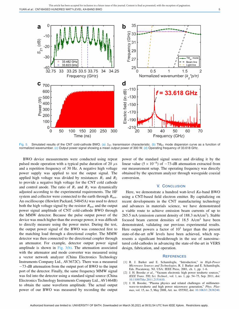
To analyze the experimental results, commercially available3-D simulation software was used. Summarized simulationsshowing the transmission characteristic, dispersion, outputpower, and operating frequency are illustrated in Fig. 5.As there are 14 cavities in the HF circuit (15 disks loaded inthe waveguide), 14 resonant frequencies have been obtained bycalculating the S21, as shown in Fig. 5(a). Our simulations con-firm the formation of two resonant frequencies at 33.482 and33.623 GHz among all of the resonant frequencies produced.Fig. 5(b) shows the dispersion curve of the TM01 mode asa function of the normalized wavenumber. The operatingvoltage of the gyrating electron beam is obtained by therelativistic velocity correction formula [41]. When operatedat 37.4 kV, and the ratio of the longitudinal velocity andtransverse velocity of the electron beam is 0.54, the beamline(longitudinal velocity line) is superimposed onto the disper-sion curve, intercepting the dispersion curve at a frequencyof 33.623 GHz. When the beam voltage decreases to 36.8 kV,the operating frequency is 33.482 GHz. These findings indicatethat the operating voltage fluctuates around 37 kV. Fig. 5(c)shows simulation results of the instantaneous output power atan operating voltage of 37.4 kV. The average output power isuncommonly large, at around 300 W (half of the instantaneousoutput power). Fig. 5(d) shows the frequency spectrum of theelectric field (in dB) in the output waveguide; the primaryfrequency mode is at 33.618 GHz, closely matching (by99.92%) the operating frequencies in our experiments. Whenthe operating voltage was set to 36.8 kV, the average outputpower is 290 W at an output frequency of 33.484 GHz, furthercorroborating our empirical findings.
IV. MATERIALS AND METHODS
Multiwalled carbon nanotubes (MWCNTs) were grown onthe sidewalls of an SS304 stainless steel truncated-cone bymicrowave plasma CVD. The SS304 substrate was coated withAl (10 nm) and Fe (1 nm) by thermal evaporation (EdwardsE306). To synthesis the CNTs, catalyst samples were placedin a 2.45-GHz microwave plasma CVD system (ASTeX). Themicrowave power level was set to 1 kW, the reactor pressureto 2500 Pa and a gas flow of 180 sccm of H2 and 20 sccm ofCH4. The growth temperature was 600 ◦C. A typical as-grownMWCNT sample is shown in Fig. 4(b).
In the CNT cold-cathode characteristic electron emissionmeasurements, diode experiments were performed using nega-tive voltage pulses. The cathode was connected to the negativehigh voltage and the control anode was connected to the earththrough a protection resistor Rp (12.8 k�) and test resistorRtest (27 �). The beam currents I were acquired by measuringthe voltage (Utest) across Rtest using an oscilloscope (HewlettPackard, 54845A). The voltage difference Uc between thecathode and the control anode was inferred by: Uc = U0 −I (Rp + Rtest), here U0 was the power supply output voltage.
Authorized licensed use limited to: UNIVERSITY OF BATH. Downloaded on March 30,2021 at 09:51:54 UTC from IEEE Xplore. Restrictions apply.
This article has been accepted for inclusion in a future issue of this journal. Content is final as presented, with the exception of pagination.YUAN et al.: CNT-BASED HUNDRED WATT-LEVEL KA-BAND BWO 5
Fig. 5. Simulated results of the CNT cold-cathode BWO. (a) S21 transmission characteristic. (b) TM01 mode dispersion curve as a function ofnormalized wavenumber. (c) Output power signal showing a mean output power of 300 W. (d) Operating frequency of 33.618 GHz.
BWO device measurements were conducted using repeatpulsed mode operation with a typical pulse duration of 20 μsand a repetition frequency of 30 Hz. A negative high voltagepower supply was applied to test the output signal. Theapplied high voltage was divided by resistances R1 and R2
to provide a negative high voltage for the CNT cold cathodeand control anode. The ratio of R1 and R2 was dynamicallyadjusted according to the experimental requirements. The HFsystem and collector were connected to the earth through Rtest.An oscilloscope (Hewlett Packard, 54845A) was used to detectboth the high voltage signal by the resistor Rtest and the outputpower signal amplitude of CNT cold-cathode BWO throughthe MMW detector. Because the pulse output power of thedevice was much higher than the average power, it was difficultto directly measure using the power meter. During the test,the output power signal of the BWO was connected first tothe matching load through a directional coupler. The MMWdetector was then connected to the directional coupler throughan attenuator. For example, detector output power signalamplitude is shown in Fig. 3(b). The attenuation associatedwith the attenuator and mode converter was measured usinga vector network analyzer (China Electronics TechnologyInstruments Company Ltd., AV3672C). There was a measured−73-dB attenuation from the output port of BWO to the inputport of the detector. Finally, the same frequency MMW signalwas fed into the detector using a standard signal source (ChinaElectronics Technology Instruments Company Ltd., AV1464B)to obtain the same waveform amplitude. The actual outputpower of our BWO was measured by recording the output
power of the standard signal source and dividing it by thelinear value (5 × 10⁻⁸) of −73-dB attenuation extracted fromour measurement setup. The operating frequency was directlyobtained by the spectrum analyzer through waveguide coaxialconversion.
V. CONCLUSION
Here, we demonstrate a hundred watt-level Ka-band BWOusing a CNT-based field electron emitter. By capitalizing onrecent developments in the CNT manufacturing technologyand advances in materials science, we have demonstrateda viable route to achieve emission beam currents of up to265.5 mA (emission current density of 188.3 mA/cm2). Stablefocused beam current densities of 18.5 A/cm2 have beendemonstrated, validating our previous experimental results.Here output powers a factor of 103 larger than the presentstate-of-the-art mW levels have been achieved, which rep-resents a significant breakthrough in the use of nanostruc-tured cold-cathodes in advancing the state-of-the-art in VERSdesign, fabrication, and operation.
REFERENCES
[1] R. J. Barker and E. Schamiloglu, “Introduction,” in High-PowerMicrowave Sources and Technologies, R. J. Barker and E. Schamiloglu,Eds. Piscataway, NJ, USA: IEEE Press, 2001, ch. 1, pp. 1–6.
[2] J. H. Booske et al., “Vacuum electronic high power terahertz sources,”IEEE Trans. THz Sci. Technol., vol. 1, no. 1, pp. 54–75, Sep. 2011, doi:10.1109/Tthz.2011.2151610.
[3] J. H. Booske, “Plasma physics and related challenges of millimeter-wave-to-terahertz and high power microwave generation,” Phys. Plas-mas, vol. 15, no. 5, May 2008, Art. no. 055502, doi: 10.1063/1.2838240.
Authorized licensed use limited to: UNIVERSITY OF BATH. Downloaded on March 30,2021 at 09:51:54 UTC from IEEE Xplore. Restrictions apply.

This article has been accepted for inclusion in a future issue of this journal. Content is final as presented, with the exception of pagination.6 IEEE TRANSACTIONS ON ELECTRON DEVICES
[4] A. A. Borisov et al., “The development of vacuum microwave devicesin Istok,” in Proc. IEEE Int. Vac. Electron. Conf. (IVEC), Bengaluru,India, Feb. 2011, pp. 437–438.
[5] J. Pasour et al., “Demonstration of a 100-kW solenoidally focusedsheet electron beam for millimeter-wave amplifiers,” IEEE Trans.Electron Devices, vol. 58, no. 6, pp. 1792–1797, Jun. 2011, doi:10.1109/Ted.2011.2126577.
[6] R. Li, C. Ruan, A. K. Fahad, C. Zhang, and S. Li, “Broadband and high-power terahertz radiation source based on extended interaction klystron,”Sci. Rep., vol. 9, no. 1, p. 4584, Mar. 2019, doi: 10.1038/s41598-019-41087-3.
[7] D. R. Whaley, R. Duggal, C. M. Armstrong, C. L. Bellew, C. E. Holland,and C. A. Spindt, “100 W operation of a cold cathode TWT,” IEEETrans. Electron Devices, vol. 56, no. 5, pp. 896–905, May 2009.
[8] M. Garven, S. N. Spark, A. W. Cross, S. J. Cooke, and A. D. R. Phelps,“Gyrotron experiments employing a field emission array cathode,”Phys. Rev. Lett., vol. 77, no. 11, pp. 2320–2323, Sep. 1996, doi:10.1103/physrevlett.77.2320.
[9] S. Berhanu et al., “Microscopic analysis of performance variationsin carbon nanotube field emission cathodes: Implications for deviceoptimization,” Phys. Status Solidi (A), vol. 209, no. 11, pp. 2114–2125,Nov. 2012, doi: 10.1002/pssa.201228296.
[10] C. Li et al., “Stable, self-ballasting field emission from zinc oxidenanowires grown on an array of vertically aligned carbon nanofibers,”Appl. Phys. Lett., vol. 96, no. 14, Apr. 2010, Art. no. 143114, doi:10.1063/1.3380597.
[11] K. B. K. Teo et al., “Microwave devices: Carbon nanotubes as cold cath-odes,” Nature, vol. 437, no. 7061, p. 968, 2005, doi: 10.1038/437968a.
[12] L. T. Williams, V. S. Kumsomboone, W. J. Ready, and M. L. R. Walker,“Lifetime and failure mechanisms of an arrayed carbon nanotube fieldemission cathode,” IEEE Trans. Electron Devices, vol. 57, no. 11,pp. 3163–3168, Nov. 2010, doi: 10.1109/TED.2010.2069563.
[13] A. M. Fennimore, D. H. Roach, G. A. Wilson, F. M. Pellicone, andL. T. Cheng, “Enhancing lifetime of carbon nanotube field emittersthrough hydrocarbon exposure,” Appl. Phys. Lett., vol. 92, no. 21,May 2008, Art. no. 213108, doi: 10.1063/1.2936960.
[14] N. S. Xu and S. E. Huq, “Novel cold cathode materials and applications,”Mater. Sci. Eng., R, Rep., vol. 48, no. 2, pp. 47–189, Jan. 2005, doi:10.1016/j.mser.2004.12.001.
[15] C. Li et al., “Carbon nanotubes: Carbon nanotubes as an ultrafast emitterwith a narrow energy spread at optical frequency,” Adv. Mater., vol. 29,no. 30, Aug. 2017, Art. no. 1701580, doi: 10.1002/adma.201770216.
[16] X. Yuan et al., “A truncated-cone carbon nanotube cold-cathodeelectron gun,” Carbon, vol. 120, pp. 374–379, Aug. 2017, doi:10.1016/j.carbon.2017.03.046.
[17] X. Yuan et al., “A gridded high-compression-ratio carbon nanotubecold cathode electron gun,” IEEE Electron Device Lett., vol. 36, no. 4,pp. 399–401, Apr. 2015, doi: 10.1109/LED.2015.2401593.
[18] Y. Saito and S. Uemura, “Field emission from carbon nanotubes and itsapplication to electron sources,” Carbon, vol. 38, no. 2, pp. 169–182,2000, doi: 10.1016/S0008-6223(99)00139-6.
[19] P. Liu, Y. Wei, K. Liu, L. Liu, K. Jiang, and S. Fan, “New-typeplanar field emission display with superaligned carbon nanotube yarnemitter,” Nano Lett., vol. 12, no. 5, pp. 2391–2396, May 2012, doi:10.1021/nl3003792.
[20] J.-W. Jeong, J.-W. Kim, J.-T. Kang, S. Choi, S. Ahn, and Y.-H. Song,“A vacuum-sealed compact X-ray tube based on focused carbonnanotube field-emission electrons,” Nanotechnology, vol. 24, no. 8,Mar. 2013, Art. no. 085201, doi: 10.1088/0957-4484/24/8/085201.
[21] H. J. Kim, J. J. Choi, J.-H. Han, J. H. Park, and J.-B. Yoo, “Design andfield emission test of carbon nanotube pasted cathodes for traveling-wave tube applications,” IEEE Trans. Electron Devices, vol. 53, no. 11,pp. 2674–2680, Nov. 2006, doi: 10.1109/TED.2006.884076.
[22] Q. Chen et al., “Study on a high beam transparency gridded X-rayelectron gun based on carbon nanotube cold cathode,” J. Nanoelec-tron. Optoelectron., vol. 13, no. 9, pp. 1265–1270, Sep. 2018, doi:10.1166/jno.2018.2364.
[23] C. M. Collins, R. J. Parmee, W. I. Milne, and M. T. Cole, “Highperformance field emitters,” Adv. Sci., vol. 3, no. 5, May 2016,Art. no. 1500318, doi: 10.1002/advs.201500318.
[24] W. I. Milne and K. B. K. Teo, “Aligned carbon nanotubes/fibersfor applications in vacuum microwave amplifiers,” J. Vac. Sci. Tech-nol. B, Microelectron., vol. 24, no. 1, pp. 345–348, Jan./Feb. 2006, doi:10.1116/1.2161223.
[25] G. Ulisse et al., “Carbon nanotube cathodes for electron gun,” IEEEElectron Device Lett., vol. 34, no. 5, pp. 698–700, May 2013, doi:10.1109/LED.2013.2250247.
[26] H. M. Manohara, R. Toda, R. H. Lin, A. Liao, M. J. Bronikowski, andP. H. Siegel, “Carbon nanotube bundle array cold cathodes for THzvacuum tube sources,” J. Infr., Millim., THz Waves, vol. 30, no. 12,pp. 1338–1350, Jul. 2009, doi: 10.1007/s10762-009-9547-x.
[27] X. Yuan et al., “A fully-sealed carbon-nanotube cold-cathode tera-hertz gyrotron,” Sci. Rep., vol. 6, no. 1, p. 32936, Dec. 2016, doi:10.1038/srep32936.
[28] X. Li, B. Chen, Y. Feng, Y. Zhang, S. Deng, and J. Feng, “Beam test ofa novel CNT cathode-based electron gun assembled in a TWT,” IEEETrans. Electron Devices, vol. 66, no. 5, pp. 2382–2388, May 2019, doi:10.1109/TED.2019.2902385.
[29] X. Yuan, M. Cole, Y. Zhang, J. Wu, W. Milne, and Y. Yan,“Parametrically optimized carbon nanotube-coated cold cathode spindtarrays,” Nanomaterials, vol. 7, no. 1, p. 13, Jan. 2017, doi:10.3390/nano7010013.
[30] Y. Xue-Song et al., “Study of pulsed field emission characteristics andsimulation models of carbon nanotube cold cathodes,” Wuli Xuebao/ActaPhys. Sinica, vol. 61, no. 21, 2012, Art. no. 216101.
[31] X. Yuan et al., “Theoretical research on a multibeam-modulated elec-tron gun based on carbon nanotube cold cathodes,” IEEE Trans.Electron Devices, vol. 63, no. 7, pp. 2919–2924, Jul. 2016, doi:10.1109/TED.2016.2565583.
[32] M. T. Cole et al., “In-situ deposition of sparse vertically alignedcarbon nanofibres on catalytically activated stainless steel mesh forfield emission applications,” Diamond Rel. Mater., vol. 23, pp. 66–71,Mar. 2012, doi: 10.1016/j.diamond.2011.12.039.
[33] M. T. Cole, K. B. K. Teo, O. Gröening, L. Gangloff, P. Legagneux,and W. I. Milne, “Deterministic cold cathode electron emission fromcarbon nanofibre arrays,” Sci. Rep., vol. 4, no. 1, p. 4840, May 2015,doi: 10.1038/srep04840.
[34] M. I. Yalandin, S. N. Rukin, V. G. Shpak, S. A. Shunailov, V. V. Rostov,and G. A. Mesyats, “Highly effective, repetitive nanosecond-range Ka-band BWO,” in Proc. IEEE Int. Power Modulators High-Voltage Conf.,May 2008, pp. 402–404.
[35] R. A. Kehs et al., “A high-power backward-wave oscillator driven by arelativistic electron beam,” IEEE Trans. Plasma Sci., vol. PS-13, no. 6,pp. 559–562, Dec. 1985, doi: 10.1109/TPS.1985.4316473.
[36] Z. Wang et al., “High-power millimeter-wave BWO driven by sheet elec-tron beam,” IEEE Trans. Electron Devices, vol. 60, no. 1, pp. 471–477,Jan. 2013, doi: 10.1109/Ted.2012.2226587.
[37] M. I. Yalandin et al., “Compact Ka-band backward-wave generator ofsuperradiative pulses operating at reduced guiding magnetic field,” IEEETrans. Plasma Sci., vol. 36, no. 5, pp. 2604–2608, Oct. 2008, doi:10.1109/Tps.2008.2004244.
[38] Q. Chen, X. Yuan, M. Cole, Y. Zhang, L. Meng, and Y. Yan, “Theoreticalstudy of a 0.22 THz backward wave oscillator based on a dual-gridded,carbon-nanotube cold cathode,” Appl. Sci., vol. 8, no. 12, p. 2462,Dec. 2018.
[39] Q. Chen et al., “Development of a K a-band circular TM01 to rectangularTE10 mode converter,” IEEE Trans. Electron Devices, vol. 67, no. 3,pp. 1254–1258, Mar. 2020, doi: 10.1109/TED.2020.2968347.
[40] W. A. de Heer, A. C. Telain, and D. Ugarte, “A carbon nanotube field-emission electron source,” Science, vol. 270, no. 5239, pp. 1179–1180,Nov. 1995, doi: 10.1126/science.270.5239.1179.
[41] A. S. Gilmour and I. Ebrary, Klystrons, Traveling Wave Tubes, Mag-netrons, Crossed-Field Amplifiers, and Gyrotrons. Fitchburg, MA, USA:Artech House, 2011, p. 21.
Authorized licensed use limited to: UNIVERSITY OF BATH. Downloaded on March 30,2021 at 09:51:54 UTC from IEEE Xplore. Restrictions apply.