a building block approach to sensornet...
TRANSCRIPT

A Building Block Approach to Sensornet Systems
Prabal Dutta, Jay Taneja, Jaein Jeong, Xiaofan Jiang, and David CullerComputer Science Division
University of California, BerkeleyBerkeley, CA 94720
prabal,taneja,jaein,fxjiang,[email protected]
ABSTRACTWe present a building block approach to hardware platformdesign based on a decade of collective experience in this area,arriving at an architecture in which general-purpose modulesthat require expertise to design and incorporate commonly-used functionality are integrated with application-specificcarriers that satisfy the unique sensing, power supply, andmechanical constraints of an application. Of course, modulesare widespread, but our focus is far less on the performanceof any individual module and far more on an overall archi-tecture that supports the prototype, pilot, and productionstages of design, and preserves the artifacts and learningsaccumulated along the way.
We present heuristics for partitioning functionality be-tween modules and carriers, and identify guidelines for theirinterconnection. Our approach advocates exporting a wideelectrical interface, eliminating the system bus, and support-ing many physical interconnect options for modules and car-riers. We evaluate this approach by constructing a familyof general-purpose modules and application-specific carriersthat achieve a high degree of reuse despite very different ap-plication requirements. We show that this approach short-ens platform development time-to-result for novice graduatestudents, making custom platforms broadly accessible.
Categories and Subject DescriptorsB.0 [Hardware]: General; B.4 [Hardware]: Input/Output& Data Communication
General TermsDesign, Experimentation, Performance
KeywordsArchitecture, Mote, Wireless, Sensor Network
Permission to make digital or hard copies of all or part of this work forpersonal or classroom use is granted without fee provided that copies arenot made or distributed for profit or commercial advantage and that copiesbear this notice and the full citation on the first page. To copy otherwise, torepublish, to post on servers or to redistribute to lists, requires prior specificpermission and/or a fee.SenSys’08, November 5–7, 2008, Raleigh, North Carolina, USA.Copyright 2008 ACM 978-1-59593-990-6/08/11 ...$5.00.
1. INTRODUCTIONSensornet platforms, like most other embedded systems,
are tightly coupled to their applications. This coupling canmake it difficult for general-purpose platforms to addressapplication-specific needs, forcing platform designers to ac-cept either suboptimal solutions or to repeatedly reimple-ment functionality. We propose a third way that composesplatforms from a two-layer hierarchy consisting of compact,general-purpose modules which provide the common func-tionality and application-specific carriers which glue togetherthese modules and also incorporate the sensors, power sup-plies, and mechanical constraints unique to the application.
Of course, sensornet platforms and modular approachesare widespread. In this paper, however, our focus is on anoverall platform architecture for supporting the three phasesof sensornet development – prototype, pilot, and production.This focus acknowledges the tensions among design trade-offs in a rapidly changing field. The desire to tackle new,unexplored problems means that rapid prototyping and “tryit and see” experimentation are very important. The widediversity of valuable applications make realistic pilot studiesat modest scale and modest investment essential, and thesehave to be well-enough executed to gain unprecedented mea-surements. And the maturing of the field means bringingthe technology into production state, reducing cost, opti-mizing performance, improving manufacturability, and ob-taining high reliability, all while preserving the learningsand artifacts accumulated along the way in moving rapidlythrough these phases of development. Despite the diversityof prior platform design efforts, it is safe to say that noneof the available options meet all of these goals, as Section 2articulates.
This paper presents a building block approach to sensor-net platform design represented by the Epic family which webelieve is the first to support all three phases of sensornetplatform development well enough for rapid forward goinginnovation. The key ideas behind this approach include sys-tematically partitioning functionality, exporting a wide elec-trical interface for modules, eliminating the system bus, andsupporting multiple ways of physically interconnecting mod-ules and carriers, from hand-soldering to machine-assembly.The specifics of this approach are presented in Section 3.
At the heart of the Epic family is a core module thatintegrates a state-of-the art microcontroller, IEEE 802.15.4radio, and flash memory onto a small, inexpensive, single-sided board with excellent RF characteristics. Following thearchitectural principles of exporting a wide electrical inter-face and minimizing logical interface constraints, the core

exposes essentially all the pins that might possibly be use-ful, including internal signals, and does not hide any of thesesignals behind a multiplexed system bus. The core can besnapped into a standard socket for prototyping, easily sol-dered to routine carrier boards for pilots, or inlined for pro-duction, according to the principle of supporting many phys-ical interconnect options. Despite this architectural focus,we recognize that modules can be only ε-suboptimal if theyare to be enthusiastically adopted. Therefore, module de-signers must go to some lengths to ensure that the basicbuilding blocks exhibit competitive performance. Section 4describes the Epic core module and its internal subsystems,introducing the key characteristics and revisiting part selec-tion with these in mind, looks at new alternatives since thecore was designed, discusses manufacturing and mechanicalconsiderations, provides a quantitative analysis of core mod-ule performance, and outlines future development directionsfor the core.
The case for a core module is clear: effective RF engineer-ing requires deep expertise to design high-frequency circuitsand specialized equipment to assemble, test, and tune them.These reasons are not limited to the core module, however.For example, a solar harvesting circuit can present a rangeof design options and subsystem choices that a designer un-familiar in the art would find difficult to navigate. Thereare other reasons to build modules as well. Some functionsare so common that reuse in modular form is inevitable.Many platforms, for example, require a USB host interfaceor battery charger, so this is an obvious module candidate.Finally, sometimes it is simply more convenient to group aset of related chips together on a board, like a handful ofdifferent memory technologies to create a memory hierarchymodule. Collectively, these principles provide some guidancefor partitioning functionality between modules and carriers.Complementing the core module is a supporting cast of spe-cialized peripheral modules that offer a handful of choicesfor complete systems, and a framework for forward goinginnovation, as Section 5 describes.
The glue for these modules are breakout and develop-ment boards or application-specific carriers. For prototyp-ing, breakout and development boards expose a wide arrayof pins and allow modules to be socketed, enabling novicesystem builders to compose platforms using simple jumperwires in a “try it and see” fashion and module developers todebug otherwise complex systems with complete freedom toaccess all exposed and intermediate signals. Section 6 ex-plains our overall vision and approach for prototyping usingthe Epic family and presents some development hardwaredesigned to support such prototyping efforts.
For pilots, inexpensive two-layer carriers are typically de-signed to fit a particular enclosure and a set of mechanicalconstraints with Epic modules being treated just like chips.For production, the modules are eliminated by incorporat-ing their contents directly into the underlying board throughhardware inlining. Section 7 evaluates the architecture byillustrating how these building blocks are used to build sev-eral simple, cost-effective, and application-specific carriersare designed using freely available CAD tools, inexpensivelymanufactured, and hand-assembled by novice graduate stu-dents. Carrier board design is so simple that it can be usedeven in an undergraduate classroom setting where studentsdo application-specific design, fabricate the boards, and as-semble a final solution in just weeks.
The final sections reflect on how effectively the Epic ap-proach meets the various contraposing design goals of thethree phases of sensornet platform development. Our ex-perience shows that the building block approach leads togreater reuse, more compact designs, increased simplicity,and lower overall part count. Not only do modules becometrue building blocks, but so do other components createdlike CAD parts and scripts. An important benefit of view-ing hardware in this way is that modules capture workinghardware designs. In the future, we envision others will cre-ate many new modules make them available to the widerresearch community.
2. BACKGROUNDIn the early stages of wireless sensor network research,
the architecture and the form factor of the platform werewide open questions. The UCLA WINS project developedWinCE-based devices about the size of a shoebox [33]; USCdeveloped PC/104 devices and proposed a tag that wouldhave a small motherboard with slots for a radio board, apower board, and sensor boards [34]; the UCB SmartDustproject developed the WeC mote with two microcontrollers,a radio, and a couple of sensors on a disk the size of a half-dollar [12]. Numerous other projects developed a variety ofARM-based systems. The Berkeley Rene mote [25] began asea change by integrating the core elements of the low-powerWeC design into a simple board with an array of commonanalog and digital interfaces organized like a conventionalsystem bus on a 51-pin connector.
The Rene design reflected a key understanding that thecommon elements across sensor network applications are sam-pling, processing, storage, and communication, while theparts that are application-specific are the sensor suite, thepower subsystem (which can support the application’s sam-ple and communication rate), and the mechanical designwhich holds the three together, exposes the sensors to thephenomena they need to sense, and protects the rest. This51-pin “AT Bus” of the sensornet world carried forward tothe MICA [25], MICA2 [3], MICAz [5], IRIS [2], and many,many other designs. Numerous sensor boards and powerboards were designed to stack on it. In many ways, it shapedsensor network research activities for over five years.
Unfortunately, the 51-pin connector proved to be unsoundfor long-term deployments in harsh conditions, and it wasexpensive relative to the other components in the system.It began to fail the Goldilocks test – instead of being “justright” it was often too general for simple applications and toolimited for demanding ones. New microcontrollers, new ra-dios, and new flash chips led to a variety of new mote designs,such as the Mica2Dot [4], Telos [32], iMote [6], BTnode [15],Eyes, TIP [7], TinyNode [18], Sensinode [8], IRIS [2], MI-CAz Stamp [5], and kMote. Each with different form factor,connectors, power requirements, and interfaces.
In hindsight, this chaos was a symptom of an underlyingtension among design tradeoffs. The rapidly changing na-ture of the field and the desire to explore novel applicationsmeant that prototyping and experimentation were very im-portant. Meanwhile, realistic pilot studies at modest scalewere essential to gain unprecedented measurements, leadingresearchers to either use commercial offerings that were oftennot quite right or design their own platforms from scratch atgreat opportunity cost. And while the maturing of the fieldmeant bringing the technology into production state, none

of the commercial offerings addressed the unique challengesin moving through the design phases, critical for preservingthe accumulated learnings and artifacts.
Despite the diversity of efforts, earlier approaches remaininadequate because they rarely address the spectrum of needsfor prototype, pilot, and production usage. We classify theseapproaches into three broad categories, bus-based, highly-integrated, and assembly-optimized, and explore their draw-backs.
The modular, stackable approach of bus-based architec-tures like WINS [33], MICA [25], iMote [6], PASTA [34],Stack [14], MASS [20], and mPlatform [29] make prototyp-ing mechanically simple but their busses can present barriersto interfacing peripherals and also result in signal conflictsif not multiplexed, and their backplanes and board stackscan be too bulky, expensive, or fragile for realistic pilot orproduction use.
The highly-integrated approach, advocated by Telos [32],bundles a mote core with sensors, antenna, and host inter-face into a single circuit board, which makes software devel-opment and desktop experimentation easy. However, withthis approach, realistic prototypes and pilots are strainedbecause too few I/O lines are exported, production costs aretoo high since many unnecessary features are integrated, andonboard sensors are not useful for many scientific purposes.
To address the various shortcomings of the bus-based andhighly-integrated approaches, vendors began to offer new,assembly-optimized module versions of their core platforms,like the MICAz [5], IRIS [2], and Tmote Mini [9]. Thesemodules, while ideal for high-volume surface-mount assem-bly, are challenging to integrate into prototype and pilotprojects because their packaging makes hand-assembly andsocketing difficult or expensive, and their relatively narrowinterfaces hide many internal signals useful for research.
3. BUILDING BLOCK APPROACHThis section presents the architecture and principles that
support the prototype, pilot, and production stages of plat-form design, and preserves the artifacts and learnings accu-mulated in their implementation. At the heart of our ap-proach are two architectural elements: the module and thecarrier. Modules are reusable, self-contained subsystems in amulti-chip module (MCM) package. Modules are composedof one or more packaged ICs and other electronic compo-nents typically found on a system board. Carriers are customcircuit board substrates that glue together general-purposemodules with application-specific sensors, power supplies,and mechanical constraints. Heuristics for partitioning func-tionality between modules and carriers are discussed in Sec-tions 4 and 5, and their effectiveness in Section 8. A sensor-net platform constructed using this building block approachis shown in Figure 1.
Several principles focus on the interface between modulesand carriers. First, we observe that a bus adds cost andcomplexity but that effective modularity does not really re-quire one. Therefore, we eliminate the system bus from amodule’s interface specification. This allows modules to beflexibly wired together in whatever way a designer sees fit,rather than being encumbered by the constraints of a genericsystem bus since it uses precious circuit board space, requirescostly or bulky or fragile connectors, complicates integrationof peripherals, and reduces generality. Extending this lineof thought, modules should export a wide electrical inter-
Figure 1: A sensornet platform designed accordingto the building block-approach. A general-purposemodule (square board) is attached to an application-specific carrier (rectangular board). The carrier in-cludes the sensor interface (large 2x3 and 2x5 head-ers), hosts a solar harvesting circuit (to the rightof the square module), and conforms to a standardenclosure (footprint and four mounting holes).
face to maximize generality and reuse potential. Finally, tosupport prototype, pilot, and production purposes, modulesshould support many physical interconnect options rangingfrom socketing to hand-soldering to machine-assembly, as§ 4.3 explores.
4. CORE MODULEEpic platforms are organized around a general-purpose
core module as well as optional peripheral modules. Thissection describes the core module, shown in Figure 2, whichis essentially the guts of a mote without the constraints onhow it can be used. The core module integrates a state-of-the-art microcontroller, IEEE 802.15.4 radio, flash memory,a 48-bit unique serial identifier, and a U.FL RF connector,all attached to a four-layer, 1 mm thick, LCC-68 form factorcircuit board one inch on a side, as Figure 3 shows.
Architecturally, the core is very similar to earlier mote de-signs like Telos [32] and MICAz, but its design is part ofa larger framework that seeks to better support the proto-typing, piloting, and production of sensornet platforms. Tobe useful for prototyping, the core module must be easy touse, debug, and profile, and it must provide good perfor-mance, sufficient storage, and ample I/O lines. To be usefulfor pilots, the core module must be easy to design-in at theCAD level, simple to hand solder at bench scales, and flex-ible when it comes to antenna choices. The core must alsobe easy to program in-circuit and debug in situ, both at thehardware and software levels. To be viable for production,the core must provide performance comparable to commer-cial modules, have an attractive cost profile, satisfy regula-tory constraints like RoHS and FCC, and be open source toallow unforeseen innovation and adaptation.
4.1 Component Choices RevisitedWhen this study was started over a year ago, a handful
of new microcontroller and radio options were available thatdid not exist when earlier platforms were designed, and to-

Figure 2: The Epic Core module: a wireless sensor-net node (“mote”) core that integrates a microcon-troller, radio, and flash memory.
day this list has grown even longer. This situation raisesthe question of whether earlier component choices still holdgiven today’s offerings. The short answer is that when thecore was designed a year ago, the answer was still yes. To-day, the answer is still (mostly) yes. Moving forward, theanswer is less clear. The rest of this section articulates thelong answer to this question.
The opportunity to revisit the core’s design raises anotherarchitectural question: what changes are needed regardless ofcomponent choice to effectively support prototype, pilot, andproduction designs? Addressing this question is a centralcontribution of this work.
4.1.1 MicrocontrollerThe microcontroller market includes many new offerings
that were not available when earlier generation mote plat-forms were designed, as Table 1 summarizes. Many of thenew offerings, like the TI MSP430F2618 and MSP430F5437are product line extensions of existing microcontrollers likethe MSP430F1611 that offer more memory, better perfor-mance, or new features. Other products, like the JennicJN5139 or Atmel ATmega1281, were not available for con-sideration until recently. Given these new choices, it is worthrevisiting why the MSP430F1611 still makes sense. Severalfactors influenced the decision to use this microcontroller,but most of the reasons are the same as the ones articulatedin the Telos mote design [32]. These include low active cur-rent, wide operating voltage range, a 16-bit sleep timer, fastwakeup from sleep, a large amount of RAM, and three directmemory access (DMA) channels that can operate while theCPU sleeps.
By these metrics, the Atmel ATmega1281 (and larger AT-mega2561) look more competitive than their predecessor,the ATmega128L. The active current has remained approxi-mately constant at 0.9 µA at 1 MHz, only about twice thatof the MSP430F1611. Since the microcontroller does notdominate the system power budget, this difference is notlikely to have a large impact on lifetime. The operating
4 SPI
SPI
SFDCCAFIFOFIFOP
2 ENA/RST
ATEST1ATEST2
RFOUTRFGND(2)
4
WPRST
RVDD
FVDD
VREF+VeREF+VeREF-
P4 / GPIO [LED(3)]3
P5 / GPIO
JTAG OSC
P6 / ADC / DAC / GPIO
P1 / GPIO
P2 / GPIO
8
8
5
4
P3 / USART / GPIO4
DVDD AVDD P4.1P1.4P1.3P1.0
P4.5/P4.6
P3/SPI0
P5/SPI1
P1.7
OSC
RST
U.FL
24
LCC-68 PAD FRAME
P2.4 ONEWIRE
MSP430F1611 CC2420
AT45DB161D
DS2411
AGND
2
RFRXTX
Figure 3: The Epic Core architecture. ATexas Instruments MSP430F1611 microcontrollerand CC2420 radio sit at the heart of the core mod-ule. An Atmel AT45DB161D NOR flash provides16 Mbit of storage. A Maxim DS2411 provides aglobally unique serial identifier. Nearly all MCU pe-ripherals are exported, including GPIO lines, ADCinputs, ADC voltage references, DAC outputs, US-ART lines, and the JTAG module. Many internalconnections between components are exported aswell.
voltage of the ATmega1281 matches the MSP430F1611 onthe low end with a minimum voltage of 1.8 V and exceedsthe MSP430F1611 on the high end at 5.5 V, providing a full1.9 V wider operating range. This can be beneficial for sys-tems that are directly connected to a lithium battery, whichsupplies between 2.6 V and 4.2 V, depending on its state ofcharge. This benefit only accrues if all system componentscan be operated over this range, which is usually not thecase today.
The ATmega1281 offers 8 KB of RAM, only 2 KB less thanthe MSP430F1611. The memory requirements for manysensornet applications make the 4 KB available on the AT-mega128L untenable. Embedded networked devices can usesignificant amounts of RAM to store message buffers whiledata collection applications can buffer sensor data in RAMfor processing or prior to writing to flash. Therefore, RAMsize is an important consideration for mote-class devices.With its 10 KB of RAM, the most among microcontrollers inits size and performance class, the MSP430F1611 remains acompetitive choice. And yet, despite this significant amountof RAM, it still has among the lowest of sleep currents (withRAM retention). Today, we see fewer complaints aboutRAM since many systems with greater RAM requirementsuse members of the Telos family. We do observe that someapplications, like TinyDB [30], require more flash memorythan the MSP430F1611 offers, and since the ATmega1281offers 128 KB and the ATmega2561 offers 256 KB, they arebetter choices for applications requiring a large code foot-print.
Despite the ATmega1281’s many improvements over theATmega128L, there are two important drawbacks that tippedthe scale in the MSP430F1611’s favor. First, the ATmega1281low-power mode timer is only 8 bits wide, meaning it hasto wakeup every 7.8 ms (using a 32 kHz clock) to service
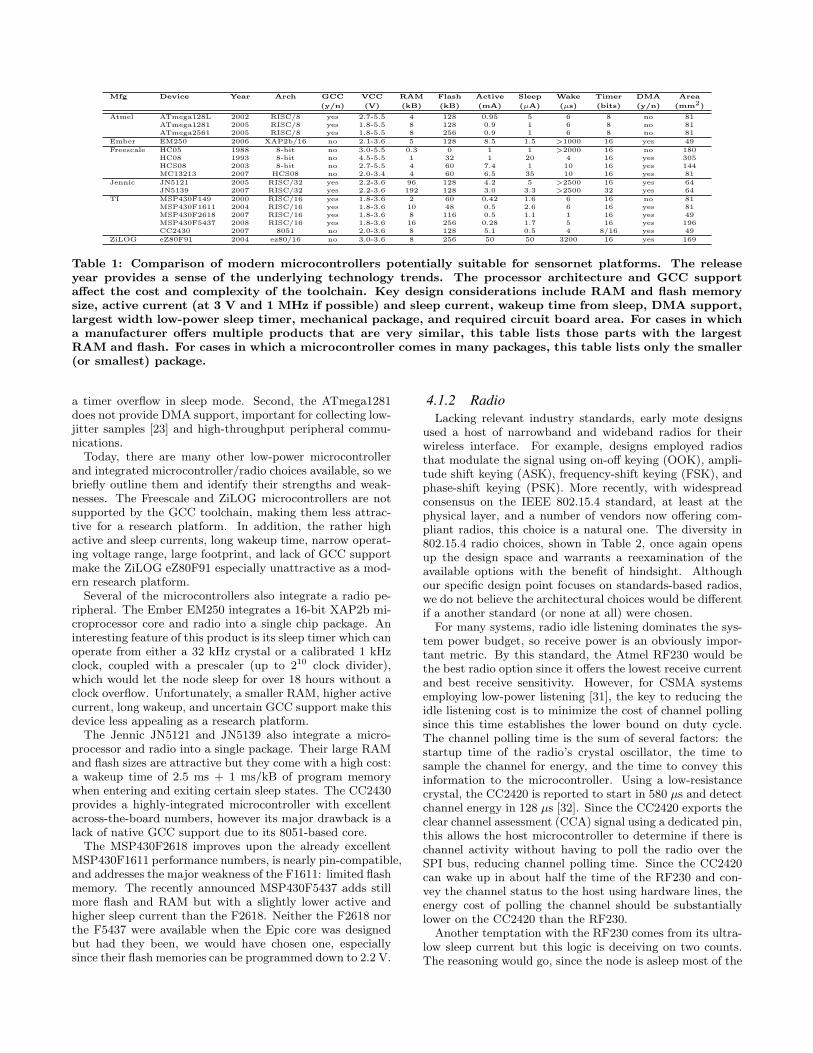
Mfg Device Year Arch GCC VCC RAM Flash Active Sleep Wake Timer DMA Area
(y/n) (V) (kB) (kB) (mA) (µA) (µs) (bits) (y/n) (mm2)
Atmel ATmega128L 2002 RISC/8 yes 2.7-5.5 4 128 0.95 5 6 8 no 81ATmega1281 2005 RISC/8 yes 1.8-5.5 8 128 0.9 1 6 8 no 81ATmega2561 2005 RISC/8 yes 1.8-5.5 8 256 0.9 1 6 8 no 81
Ember EM250 2006 XAP2b/16 no 2.1-3.6 5 128 8.5 1.5 >1000 16 yes 49Freescale HC05 1988 8-bit no 3.0-5.5 0.3 0 1 1 >2000 16 no 180
HC08 1993 8-bit no 4.5-5.5 1 32 1 20 4 16 yes 305HCS08 2003 8-bit no 2.7-5.5 4 60 7.4 1 10 16 yes 144MC13213 2007 HCS08 no 2.0-3.4 4 60 6.5 35 10 16 yes 81
Jennic JN5121 2005 RISC/32 yes 2.2-3.6 96 128 4.2 5 >2500 16 yes 64JN5139 2007 RISC/32 yes 2.2-3.6 192 128 3.0 3.3 >2500 32 yes 64
TI MSP430F149 2000 RISC/16 yes 1.8-3.6 2 60 0.42 1.6 6 16 no 81MSP430F1611 2004 RISC/16 yes 1.8-3.6 10 48 0.5 2.6 6 16 yes 81MSP430F2618 2007 RISC/16 yes 1.8-3.6 8 116 0.5 1.1 1 16 yes 49MSP430F5437 2008 RISC/16 yes 1.8-3.6 16 256 0.28 1.7 5 16 yes 196CC2430 2007 8051 no 2.0-3.6 8 128 5.1 0.5 4 8/16 yes 49
ZiLOG eZ80F91 2004 ez80/16 no 3.0-3.6 8 256 50 50 3200 16 yes 169
Table 1: Comparison of modern microcontrollers potentially suitable for sensornet platforms. The releaseyear provides a sense of the underlying technology trends. The processor architecture and GCC supportaffect the cost and complexity of the toolchain. Key design considerations include RAM and flash memorysize, active current (at 3 V and 1 MHz if possible) and sleep current, wakeup time from sleep, DMA support,largest width low-power sleep timer, mechanical package, and required circuit board area. For cases in whicha manufacturer offers multiple products that are very similar, this table lists those parts with the largestRAM and flash. For cases in which a microcontroller comes in many packages, this table lists only the smaller(or smallest) package.
a timer overflow in sleep mode. Second, the ATmega1281does not provide DMA support, important for collecting low-jitter samples [23] and high-throughput peripheral commu-nications.
Today, there are many other low-power microcontrollerand integrated microcontroller/radio choices available, so webriefly outline them and identify their strengths and weak-nesses. The Freescale and ZiLOG microcontrollers are notsupported by the GCC toolchain, making them less attrac-tive for a research platform. In addition, the rather highactive and sleep currents, long wakeup time, narrow operat-ing voltage range, large footprint, and lack of GCC supportmake the ZiLOG eZ80F91 especially unattractive as a mod-ern research platform.
Several of the microcontrollers also integrate a radio pe-ripheral. The Ember EM250 integrates a 16-bit XAP2b mi-croprocessor core and radio into a single chip package. Aninteresting feature of this product is its sleep timer which canoperate from either a 32 kHz crystal or a calibrated 1 kHzclock, coupled with a prescaler (up to 210 clock divider),which would let the node sleep for over 18 hours without aclock overflow. Unfortunately, a smaller RAM, higher activecurrent, long wakeup, and uncertain GCC support make thisdevice less appealing as a research platform.
The Jennic JN5121 and JN5139 also integrate a micro-processor and radio into a single package. Their large RAMand flash sizes are attractive but they come with a high cost:a wakeup time of 2.5 ms + 1 ms/kB of program memorywhen entering and exiting certain sleep states. The CC2430provides a highly-integrated microcontroller with excellentacross-the-board numbers, however its major drawback is alack of native GCC support due to its 8051-based core.
The MSP430F2618 improves upon the already excellentMSP430F1611 performance numbers, is nearly pin-compatible,and addresses the major weakness of the F1611: limited flashmemory. The recently announced MSP430F5437 adds stillmore flash and RAM but with a slightly lower active andhigher sleep current than the F2618. Neither the F2618 northe F5437 were available when the Epic core was designedbut had they been, we would have chosen one, especiallysince their flash memories can be programmed down to 2.2 V.
4.1.2 RadioLacking relevant industry standards, early mote designs
used a host of narrowband and wideband radios for theirwireless interface. For example, designs employed radiosthat modulate the signal using on-off keying (OOK), ampli-tude shift keying (ASK), frequency-shift keying (FSK), andphase-shift keying (PSK). More recently, with widespreadconsensus on the IEEE 802.15.4 standard, at least at thephysical layer, and a number of vendors now offering com-pliant radios, this choice is a natural one. The diversity in802.15.4 radio choices, shown in Table 2, once again opensup the design space and warrants a reexamination of theavailable options with the benefit of hindsight. Althoughour specific design point focuses on standards-based radios,we do not believe the architectural choices would be differentif a another standard (or none at all) were chosen.
For many systems, radio idle listening dominates the sys-tem power budget, so receive power is an obviously impor-tant metric. By this standard, the Atmel RF230 would bethe best radio option since it offers the lowest receive currentand best receive sensitivity. However, for CSMA systemsemploying low-power listening [31], the key to reducing theidle listening cost is to minimize the cost of channel pollingsince this time establishes the lower bound on duty cycle.The channel polling time is the sum of several factors: thestartup time of the radio’s crystal oscillator, the time tosample the channel for energy, and the time to convey thisinformation to the microcontroller. Using a low-resistancecrystal, the CC2420 is reported to start in 580 µs and detectchannel energy in 128 µs [32]. Since the CC2420 exports theclear channel assessment (CCA) signal using a dedicated pin,this allows the host microcontroller to determine if there ischannel activity without having to poll the radio over theSPI bus, reducing channel polling time. Since the CC2420can wake up in about half the time of the RF230 and con-vey the channel status to the host using hardware lines, theenergy cost of polling the channel should be substantiallylower on the CC2420 than the RF230.
Another temptation with the RF230 comes from its ultra-low sleep current but this logic is deceiving on two counts.The reasoning would go, since the node is asleep most of the

Mfg Device Year Wake VCC RxSens TxPwr Rx Tx Sleep FIFO SCLK SFD CCA AES Area
(ms) (V) (dBm) (dBm) (mA) (mA) (µA) (Rx/Tx) (MHz) (y/n) (y/n) (y/n) (mm2)
Atmel RF230 2006 1.1 1.8-3.6 -101 +3 15.5 16.5 .02 128 8.0 no no no 25Ember EM260 2006 1 2.1-3.6 -99 +2.5 28 28 1.0 128 5 yes yes yes 36Freescale MC13192 2004 7-20 2.0-3.4 -92 +4 37 30 1.0 128/256 8.0 yes yes yes 25
MC13202 2007 7-20 2.0-3.4 -92 +4 37 30 1.0 128/256 8.0 yes yes yes 25MC13212 2005 7-20 2.0-3.4 -92 +3 37 30 1.0 128/256 8.0 yes yes yes 81
Jennic JN5121 2005 >2.5 2.2-3.6 -93 +1 38 28 <5.0 16 16.0 yes yes yes 64JN5139 2007 >2.5 2.2-3.6 -95.5 +0.5 37 37 2.8 16 16.0 yes yes yes 64
TI CC2420 2003 0.58 2.1-3.6 -95 0 18.8 17.4 1 128/128 10 yes yes yes 49CC2430 2005 0.65 2.0-3.6 -92 0 17.2 17.4 0.5 128/128 4 yes yes yes 49CC2520 2008 0.50 1.8-3.8 -98 +5 18.5 25.8 .03 128/128 8.0 yes yes yes 25
Table 2: Comparison of modern IEEE 802.15.4-compatible radios. The release year provides a sense of theunderlying technology trends. The wakeup time (wake) is the time required to transition the radio fromsleep to listen. The receive sensitivity (RxSens) is a measure of the minimum signal strength needed forsuccessful reception. The transmit power (TxPwr) is the output power of the radio. Rx, Tx, and Sleep arethe receive, transmit, and sleep current draws. The amount of the receive and transmit data path bufferingis available (FIFO). The speed of the data bus (SCLK) limits the rate of data input/output to/from theradio from the host microcontroller. The start-of-frame-delimiter (SFD) is a hardware handshake signal thattoggles at a well-defined point during packet transmission or reception. The clear-channel-assessment (CCA)is a hardware handshake signal that indicates whether the channel power exceeds the clear channel threshold.The advanced encryption system (AES) indicates whether hardware support for encryption is included in theradio.
time, sleep current matters a great deal. While this maybe true in theory, in practice the constant factors dominate.First, the sleep cost must consider sleep currents aggregatedover all components, and the lowest microcontroller currentis 25 times larger at 500 nA. Second, for systems that operatearound 1% duty cycle, but use a radio whose active currentto sleep current is 10000:1 or higher like the RF230, energyconsumed in the sleep state pales in comparison to energyconsumed in the active state. Recent research has demon-strated radio operation at permille (0.1%) duty cycles, mak-ing sleep currents more important yet still not among themost important of factors.
The RF230 also offers better receive sensitivity than theCC2420 (-101 dBm vs -95 dBm) and higher transmit power(+3 dBm vs 0 dBm), so its link budget is about 9 dB higherthan the CC2420. This translates to either longer-rangeor lower-power communications since transmit power is ad-justable. Finally, a shared send/receive FIFO and the lackof hardware support for AES means this cryptographic func-tion must occur in MCU software, rather than in optimizedhardware.
Today, there are many other 802.15.4-compliant radio choices,so we briefly outline some of them and identify some of theirstrengths and weaknesses. The EM260 appears to offer ex-cellent receive sensitivity and transmit power, at the expenseof higher current draws and a constrained development en-vironment. The Freescale family of radios offer an order ofmagnitude longer wakeup times, in the range of 7-20 ms,than the CC2420 as well as much higher current draws.The Jennic JN5121 and JN5139 are attractive because oftheir large RAM and 32-bit core, but their 2.5 ms minimumwakeup latency is long, and still longer if RAM retention isdisabled and the program must be copied to RAM from flashon each wakeup. The CC2430 appears to be an excellent,highly-integrated system with ample RAM and flash. Theonly downsides are low receive sensitivity and a lack of GCCtoolchain support. Finally, the CC2520 offers nearly all ofthe benefits of the CC2420 and RF230. If this radio hadbeen available when the core was designed in early 2007, wewould have selected it.
For these reasons, the CC2420 still provided the best over-all power profile at the time of the Epic core design, ce-
menting our decision to use it in the core module. To en-sure a low radio wakeup similar to Telos, the core’s radiooscillator circuit is built around a Hong Kong Xtal’s C5Mfamily 16 MHz crystal. This decision was inspired by obser-vations that showed the benefits of choosing a crystal witha low series resistance, namely allowing the radio to startup quickly [32]. This crystal’s lines are also exported usingshort traces to allow oscillator quick start circuits to be ex-plored using this module [16]. If such a circuit is added, caremust be taken to ensure that capacitive loading of the crys-tal does not exceed the manufacturer’s recommended toler-ances. Our evaluation of the Epic core in Section 4.4 showsthat its wakeup performance tracks that of Telos.
The CC2420 also provides a pair of test lines, ATEST1and ATEST2. These lines can be programmed to output arange of internal signals at various stages of the signal pro-cessing pipeline. Although normally intended for productiontesting, these signals can provide the low-level access neededto implement analog network coding [27] or interference can-cellation [24]. The radio SPI bus, CCA, and SFD lines arealso exported from the module, simplifying external probingand allowing external hardware to count both the numberof times these signal are asserted as well as the amount oftime they remain asserted. These are important indicatorsof channel activity, availability, and interference.
4.1.3 FlashThe core uses an AT45DB161D NOR flash [1] that pro-
vides 16 Mbit of non-volatile storage. Although this chiphas a higher sleep current than the ST M25P80 [11] usedin Telos, the dual RAM buffers simplify driver software andallow data to be accessed from one buffer over the SPI inter-face while the other buffer is busy reading from or writingto non-volatile storage.
There are two core module designs that only differ in theway the flash memory is connected to the MCU. In one con-figuration, the radio and flash are on the same bus (SPI0),preferable for workloads where the node is connected withanother serial device, like a host computer or a sensor withan RS-232 port. In the other configuration, the flash andradio are on different buses, SPI0 and SPI1, respectively,desirable for nodes that do not use their UART, like routers

in a mesh network, since resource contention will not occurand SPI bandwidth does not have to be shared.
The flash memory has a write-protect line that is exportedbecause there is no broadly appropriate default. Accordingto one school of thought, a “boot sector” should always bewrite-protected unless the module is being reprogrammedthrough physical connection to a programming board or hostcomputer; however, there is no simple and fool-proof wayfor the module to determine this unambiguously. Accordingto another school of thought, the default behavior of themodule should be to allow the flash to be reprogrammedin its entirety. The issue boils down to a policy decision,so in the interest of end-user flexibility, this line is neitherdriven nor pulled high or low – the platform developer hasthe option to pull-up this line by populating a resistor onthe core module.
4.2 Implementation DecisionsThis section presents several implementation choices that
focus on component interconnections, I/O exports, and sup-ply circuitry that have architectural motivations like “exporteverything” and “minimize constraints.”
4.2.1 Component Interconnections and ExportsThe MCU communicates with the radio using an SPI bus
(USART0), receives status information (CCA, FIFO, andFIFOP) from the radio using three interrupt-capable inputlines and packet transmission/reception timing (SFD) fromthe radio using one timer capture register, and controls andresets the radio using a pair of output lines. The MCU com-municates with the flash memory using SPI on either US-ART0 or USART1 and communicates with the serial iden-tifier chip using a single, interrupt-capable, GPIO line withpull-up to implement Dallas Semiconductor’s 1-wire proto-col. The MCU exports a byte-wide port to simplify the in-terface to devices with a byte-wide bus interface like NANDflash memory, FIFOs, and high-speed parallel ADCs.
In addition to the communications and control interfacesshared with the MCU, the radio also exports a wireless in-terface and some useful test lines. The wireless port passesthrough a balun and is routed to both a 50-ohm RF porton the LCC-68 module as well as a U.FL connector onboardthe module circuit board. A single capacitor selects whichway the RF signal goes – LCC-68 pad or U.FL connector.This flexibility allows developers to choose either an exter-nal antenna with a U.FL-terminated pigtail – now commonbecause of 802.11 b/g radios – or a board-integrated antennalike a chip antenna or a planar-inverted F-antenna (PIFA).The first choice eliminates low-level RF engineering whilethe second choice allows for a more compact solution.
4.2.2 Power, Ground, and ReferencesThe core exports four different power supply lines for the
four major power domains: DVDD supplies the microcon-troller core and serial identifier, AVDD supplies the ADCcore and reference, RVDD supplies the radio, and FVDDsupplies the external flash memory. These signals may betied together externally, connected to different supplies withslightly different voltages, or individually passed throughcurrent sense resistors to allow current profiling per powerdomain. All of the supply lines are internally decoupled us-ing 0.1 µF capacitors. If long external power traces are used,larger external capacitors should be used. The core also ex-
ports several references used by the ADC. The VREF+ lineallows the internal ADC reference to be used by externalcircuitry (with appropriate buffering). The VeREF+ andVeREF- lines allow externally-generated high and low refer-ences to be used by the ADC.
In addition to the four supply lines, the core exports fourdifferent ground lines. Although three of these ground linesare internally connected, they individually provide the pref-erential ground return for the microcontroller, radio, andflash memory. The fourth ground line, AGND, connects toan isolated ground plane section and provides the return forthe analog section of the microcontroller. The AGND can beconnected to the digital grounds externally, but care mustbe taken to reduce digital noise from coupling with AGND.Finally, the radio ground is divided into a digital sectionand an analog section with a separate ground, RFGND. Theradio digital section shares a common ground with the mi-crocontroller and flash while RFGND provides the returnfor the RF path. The point where the RFGND lines are ex-ported from the module is the only place where the analogand digital grounds are connected together – the proverbial“ground mecca”– situated on the ground ring along the mod-ule perimeter, providing a convenient solder point for an RFshield.
4.3 Mechanical DesignA question that every module designer must confront at
some point is what form factor and connector interface shouldthe module use? There are nearly as many different answersto this question as there are mote platforms. The Epic coremodule uses an industry-standard LCC-68 (68-pin leadlesschip carrier) form factor that places all parts on one sideof the module circuit board and exposes nearly every sig-nal that might possibly be useful along the board edge viaperimeter pads. This packaging wastes no connector spacesince the board edge is otherwise unused, allows a seam-less transition from prototype to production since modulescan socketed, hand-soldered, or machine-assembled, and asingle-sided board makes signal probing easy.
Several considerations played a role in the choice of perime-ter pads. First, since the package is leadless, no costs areincurred on connectors. Second, since the package land pat-tern is essentially JEDEC-compliant (except for pin num-bering), an off-the-shelf prototype or production socket canbe used to program the device or break out the signal linesfor debugging. Third, since the 68 pads around the mod-ule perimeter are actually plated-through semi-holes (alsoknown as castellations or routed vias), they are easy to solderby hand which greatly simplifies prototyping. Fourth, sincethe plated-through semi-holes are concave, an oscilloscope orvoltmeter probe tip rests easily in them, making debuggingjust a bit easier. Fifth, since the plated-through semi-holesare actually vias that connect all layers of the circuit board,they reduce the number of vias that might otherwise be nec-essary, potentially reducing cost and providing more circuitboard real estate.
Superficially, the Epic core’s LCC-68 footprint might seemsimilar to the the MICAz [5] and IRIS [2] OEM modules orthe Tmote Mini [9], but there are some important differencesthat make Epic well-suited to pilot studies: it can be hand-soldered, it has a wide interface that exports nearly everyinternal signal, and it can be socketed. This design consid-eration raises an important architectural question: should

−25 −20 −15 −10 −5 0−100
−80
−60
−40R
SS
I (d
Bm
)
EpicTelos
−25 −20 −15 −10 −5 095
100
105
110
Transmit Power (dBm)
LQ
I
Figure 4: Radio reception performance (RSSI andLQI) of Epic and Tmote Sky over the same channelas the transmit power is swept from -25 to 0 dBm.
the number of pins a module exports grow linearly with itsarea or as the square root? A ball grid array (BGA) al-lows a linear relationship between area and pin count whilethe perimeter pins of a leadless chip carrier (LCC) grows asthe square root of the area. We chose an LCC-68 packagewith plated-through semi-holes to allow hand assembly, buta side-effect of the decision is that modules are more limitedin their I/O width. We also experimented with differentmodule thicknesses and found that an 0.5 mm board wastoo flimsy (without a structural shield) and that the stan-dard 1/16 in circuit board was unnecessarily thick, so wesettled on a module thickness of 1.0 mm.
Other mote designs, like the MICA family including theMICA, MICA2, and MICAz often waste circuit board real-estate unnecessarily making them too large to comfortablydesign into enclosures, require expensive and fragile connec-tors, and do not export many I/O lines useful for researchand experimentation. The highly-integrated Telos suffersfrom many of these same problems. The MICA2Dot [4] ismore space-optimized and integrates the core pieces better,buts its limited I/O lines reduce choice, its connector is diffi-cult to attach, and its antenna connector is poorly matched.
4.4 EvaluationModules will only be adopted if their performance is at
most ε-suboptimal to other alternatives, and we show herethat Epic compares favorably to earlier work. One of thekey metrics for a platform is the radio wakeup time. Wemeasured the wakeup time of both Epic and Telos by moni-toring the state of the CC2420’s CCA pin in the same waythat the TinyOS 1.x and 2.x stacks use to determine whenthe oscillator has stabilized. In our experiments, Epic wakesup in 629± 3µs while the Telos wakes up in 619± 3µs (95%confidence).
Sleep current is another important performance metricwhich for Epic is 7 µA at 3 V. In comparison, we measuredthe Telos sleep current to be 6 µA at 3 V when running theTinyOS Null application. Although the Epic sleep currentis comparable to Telos, the constituent currents are differ-ent: most of the Epic current draw comes from the flash
chip while most of the Telos current draw comes from itshost interface, which Epic removes for reasons of generality.
To evaluate radio reception, a transmitter node (Telos B)is positioned 3 m from a fixed antenna. In the first experi-ment, a Sentilla Tmote Sky [10] is connected to the antenna.In the second experiment, an Epic is connected to the sameantenna. During each experiment, 20 packets are transmit-ted from the sender to the receiver. The received signalstrength indicator (RSSI) and link quality indicator (LQI)are logged. This experiment is repeated at eight differentpower levels. These results, along with tests over a range ofchannels and distances, confirm that the RF performance ofEpic is commensurate with a mature commercial system.
As a cautionary note, we point out that achieving thisperformance required months of design, evaluation, tuning,and redesign. This work was carried out using expensivetest and measurement equipment including high-speed digi-tal oscilloscopes, spectrum analyzers, and network analyzers.In the final analysis, ten different RF section layouts, threedifferent inductor choices, and two different RF ports wereevaluated. All of our designs are open-sourced and availableonline.
4.5 Future DirectionsIn hindsight, the choice of the MSP430F1611 microcon-
troller and CC2420 radio have stood the test of time, andproduct line extensions like the MSP430F26x, MSP430F54x,and CC2520 promise a simple migration pathway forward.An obvious next-generation core module will be an evolu-tionary one that integrates these much improved but stillbackward-compatible parts. This path will allow the com-munity to leverage existing investments in software yet allownew research efforts by moving more functionality into theradio, and making the processor-radio interface richer andmore flexible. At the same time, new products from othervendors are quickly closing, or have already closed, the gapin wakeup latency, RAM size, low-power timer support, di-rect memory access, and operating voltage range.
5. EXPERT PERIPHERAL MODULESComplementing the core module are a family of peripheral
modules that provide specific functions, such as power sup-ply conditioning, high speed host communication interfaces,bulk storage, or analog signal conditioning. Figure 6 showsthe modules currently in the Epic family.
(a) Core (b) Storage (c) USB
Figure 6: Core, storage, and USB Epic modules.
Since a key aspect of the architectural approach is a sys-tematic partioning of functionality between modules andcarriers, we identify four cases when modules make sense:when their design requires deep expertise, when their as-sembly or tuning requires specialized equipment, when theirfunction is so common that reuse in modular form is in-evitable, and when it is simply more convenient to group a

(a) Development Board (b) Interface Board (c) Breakout Board (d) COTS Parts
Figure 5: The Epic family includes hardware specifically designed for (a) making platform prototyping possiblein a classroom setting by novice designers (b) interfacing with the popular Phidgets analog and digital sensors(c) empowering module designers to construct, probe, and debug intricate circuits on-the-fly, both only using(d) off-the-shelf parts such as jumpers, sensors, solar power packs, and surfboards.
set of related components. Collectively, these principles pro-vide some guidance for partitioning functionality betweenmodules and carriers and they address the question: wheredo modules come from? Following these heuristics, Table 3traces the genesis of the modules currently in the Epic family,and the remainder of this section discusses their functions.
Deep Special Modular SimpleModule Expertise Equip. Reuse Convenience
Core yes yes yes noUSB no no yes yes
Storage no yes no yes
Table 3: The genesis of core and peripheral modulesin the current Epic family. Modularizing a compo-nent is beneficial if it demands deep expertise to de-sign, requires specialized equipment to assemble ortune, is general enough that reuse in modular formis inevitable, or just as a way to group together re-lated parts into a subsystem as a matter of simpleconvenience.
The USB module provides four functions: host interface,reprogramming, JTAG over USB (requires additional hostsoftware), and battery charging and management. The firstthree offer the same functionality as the Telos [32] in that thehost interface and reprogramming functions are multiplexedusing the same I/O lines and JTAG over USB is possible (butnot supported). The battery charging and management canrecharge a Lithium battery whenever the module is pluggedinto a USB port and arbitrate between USB power and anattached Lithium (or alkaline) battery. This module wasbuilt because it was perceived to be quite useful to a numberof platforms in modular form and was a convenient containerfor related functionality.
The storage module integrates four different non-volatilememory chips – a 1 Gbit NAND flash, two 16 Mbit NORflashes, and one 512 Kbit FRAM. These memory chips havevery different read, write, and erase characteristics and sothey represent a useful collection of chips integrated on asingle module for simple convenience when researching stor-age systems. Additionally, some of the included flash chipsare in packages that are either leadless or with extremelysmall pitch, making them difficult to hand solder and war-ranting specialized manufacturing equipment. This modulewas built both for experimentation and as a storage subsys-tem for motes.
6. PROTOTYPINGIn our vision for prototyping, platform developers are able
to pick a handful of components like sensors, motes, bat-tery packs, and solar harvesting modules, and literally wirethem together in whatever way is most appropriate. Writ-ing the corresponding system software would follow a simi-lar pattern; most components would have associated driversthat could simply be declared and wired to the hardwareresources they use, like GPIO lines, ADC channels, or anSPI bus. We envision the emergence of platform construc-tion kits that include an assortment of building blocks, theirassociated driver software, and the glue to assemble a widevariety of prototype nodes. In this section, we examine howEpic supports prototyping approaches for both novice andadvanced system designers.
6.1 Try It And SeeMany projects begins with experimentation and rapid pro-
totyping inspired by a “try it and see” attitude. The goal isto demonstrate a basic implementation that showcases animportant capability, enables some exploratory data to becollected, or reduces perceived implementation risk throughan existence proof. At this stage of the game, maximum im-pact demands a narrow focus on the essential elements of thesystem, but the other parts must be good enough to evaluatethe prototype. The metric of merit is time-to-result.
Unfortunately, several factors increase time-to-result. Is-sues like sensor and power supply selection, electrical wiring,and device driver development dominate engineering effortswhile more novel aspects like application software, perfor-mance characterization, and end-user data collection are rou-tinely back burnered during the initial stages. To improveproductivity, we created a Development Board that can beeasily and inexpensively integrated with off-the-shelf sensors,displays, and solar packs to improve time-to-result.
Figure 5(a) shows the Development Board, which benefitsfrom the choice of an industry-standard LCC-68 footprint byincluding an off-the-shelf socket for easily swapping modules.Adhering to the principle that all signals should be availableto the platform designer, breakout pins allow access to everysignal, simple shorting shunts allow each signal to be indi-vidually connected to power or ground, and jumper wiresallow a signal to be easily connected to off-the-shelf partslike the ones shown in Figure 5(d).
The Development Board also incorporates a USB modulefor programming, alkaline and lithium battery connectionsfor supplying power, and LEDs and buttons for feedback,

debugging, and control. This flexible platform enables quickprototyping and exploration of novel development elementswhile circumventing the complexities of module and carrierdesign. The board has already been used by undergradu-ate students to develop application-specific platforms and asecond version, shown in Figure 5(b), was used to teach asummer school on wireless embedded systems.
6.2 DebuggingDebugging is an often frustrating aspect of prototyping.
Effective debugging requires the developer to probe signalvoltages to verify circuit operation and measure currents toidentify unexpected draws and verify expected ones. Unfor-tunately, many systems can make probing signals and de-bugging painfully difficult: signals are buried under chips,routed through to intermediate layers of the printed circuitboard, and never exposed through any header. Measuringcurrents can be still more challenging since it requires break-ing a circuit to take the measurement. In most systems, di-rectly measuring the individual draws of the microcontroller,radio, flash, or other peripherals is impossible since the in-dividual power supply lines are buried in the circuit boardand a single, global power supply line is exposed. The resultis that developers must write test code that isolates differ-ent functions, rather than being able to directly observe thesystem running application code.
To address these challenges of hardware debugging, wedeveloped a breakout board, shown in Figure 5(c), thatincludes an LCC-68 socket, pins for easily accessing andjumpering each signal, and an Epic programming port. Withaccess to the full array of signals, hardware developers caneasily probe every point in a design, connecting the circuit,multimeters, oscilloscopes, and other monitoring equipmentas they see fit.
7. CARRIER BOARD CASE STUDIESCarriers are circuit boards that act as substrates to glue
together general-purpose modules with application-specificsensors, power supplies, and mechanical constraints. To eval-uate the utility of our proposed architecture, we designedand implemented several different pilot-stage carrier boards.These case studies illustrate how our decomposition allowsnew platforms to be designed quickly by novice graduatestudents (usually in a few days), fabricated inexpensively ontypically two-sided circuit boards (for a few hundred dollars),and easily hand-assembled (in hours, by the same studentswho designed the carriers). Table 4 summarizes these carri-ers and their differences.
Carrier Modules Sensors Power Mechanical
HydroWatch Core T, H, L solar enclosureACMeter Core V, C AC enclosure
BenchMark Core, USB T, H, L USB Telos-likeMeraki Core T, H Meraki Meraki
Table 4: Despite their unique application require-ments, all carriers incorporate the same mote core.Sensors: temperature (T), humidity (H), light (L),voltage (V), and current (C).
7.1 External Sensor and SolarThe literature on sensornet applications shows many plat-
forms built for monitoring animals and the environment, a
subset of which employ a solar power subsystem for sus-tainable operation including ZebraNet [26, 39] for trackingthe location of zebras in African savanna and jungle, SolarDust [35] for measuring the penetration of light under shrubthickets in former grasslands, and Fleck [36] for measuringsoil moisture and tracking livestock behavior on farms.
Building on this line of research, we have developed anew platform to study to the hydrological cycle in forestedenvironments. Each microweather sensing node, shown inFigure 7(a), consists of a small waterproof box containinga carrier board, batteries, and carefully exposed tempera-ture, relative humidity, and light sensors [37]. Addition-ally, RF requirements in the moist, dense forest require ahigh-gain antenna; thus, we export the U.FL connector pro-vided by the Epic core module to an SMA connector and usean externally-attached 7-dBi omnidirectional antenna. Thecarrier board, shown in Figure 1, incorporates an Epic coremodule, a solar energy harvesting circuit with voltage andcurrent monitoring, the iCount [19] system for measuringsystem energy consumption, and connections for the sen-sors. This 2-layer PCB was created using the freeware EagleCAD Tool in less than two days and fabricated at a unit costof $10.83 for a 60 piece build with a five day leadtime. Theboard took under two hours to populate by hand.
Previous incarnations of the HydroWatch node were builtaround a Telos family mote, resulting in a larger form fac-tor (twice the enclosure size), insufficient exposed GIO andADC pins (some desired measurements could not be taken),and a significantly higher cost (the Telos cost three timesas much as the Epic). The new HydroWatch node designremedies these issues while achieving similar RF and en-ergy performance. In terms of board fabrication cost, theprevious 2-layer HydroWatch PCB took about a week todesign, took two revisions to become operational, and cost$11.59 per board for a 54 piece build with a five day lead-time. Indeed, the Epic platform design flow has improveddesign flexibility while reducing time-to-result with compa-rable fabrication cost to previous methods.
7.2 AC Power MonitoringMonitoring building energy consumption is an important
opportunity for savings in an increasingly energy-consciousera; in fact, many AC power metering and control devicesalready exist and some are even network-enabled [28, 13].However, since these are either commercially unavailable orcost prohibitive, we developed a platform for AC power me-tering, seen in Figure 7(b), to support research in energy-aware decision-making in datacenter and home environmentsboth inexpensively and at scale. This platform includes aTRIAC for switching the AC load on and off, and an Epiccore module for wireless communications.
The primary sensor of this platform is an industry stan-dard IC that measures real, apparent, and reactive power byusing a manganin current sensing resistor. Though the ACelectricity presents a convenient source of power, the highmains voltage must be reduced, rectified, and regulated, forthe DC circuitry including the Epic core module and relatedcomponents. A standard approach is to use a transformerand a bridge rectifier, but this can be bulky. Recognizingthe minimal DC current requirements of our design, a morecost-effective and space-saving way is to simply use capaci-tor dividers and a pair of diodes to shave off a small amountof AC current. This specialized design effort will not need

(a) HydroWatch Board (b) ACMeter Board (c) BenchMark Board (d) Meraki Daughterboard
Figure 7: Platforms for different applications have been built to evaluate the Epic architecture: (a) anenvironmental monitoring node incorporating solar energy harvesting and application energy metering, (b)an AC electricity meter for measuring building energy use, (c) a platform for sensornet testbeds with a USBinterface, application energy metering, and a FIFO buffer for collecting and streaming high-frequency data,and (d) a Meraki Mini daughterboard that connects 802.3 and 802.11-based IP networks to 6lowpan-basedsensor networks. Each platform was designed in less than a week using the same generalized core modulewhile satisfying the specific requirements of the application.
to be repeated; the circuit can be replicated in future AC-powered platforms. One drawback to this approach is thefloating ground, which may not be ideal for an experimentaldevice, suggesting an isolation transformer may be a betterchoice for future revisions.
For the enclosure, rather than formulating a custom de-sign, often both costly and time consuming, we selected theenclosure of an off-the-shelf AC power meter and designedour PCB within its restrictions. Thus, the board needed toaccommodate not only a standard NEMA 5-15 AC plug andreceptacle, but also a number of holes and contact points im-posed by the clip design of the off-the-shelf enclosure. Sincethe Epic core module is a thin single-sided board, we wereable to incorporate it easily within our volume constraintswithout facing the difficulty of connecting and accommodat-ing a separate, larger mote inside the enclosure.
Additionally, we included an optically-coupled TRIAC toenable remote control of the current flowing to appliancesconnected to this AC meter. The TRIAC can also be used asa dimmer when combined with a zero-crossing output fromthe AC measurement chip. To save space and cut cost, weused a Planar Inverted-F Antenna (PIFA). Switching fromthe default U.FL antenna connector on the Epic core mod-ule involves switching a single capacitor. More challenging,however, is the RF engineering needed to match the Epiccore, microstrip, and PIFA antenna. The antenna and itsfeedline are available as a script, allowing a simple way tochange important parameters.
The design process for this board took one week using Ea-gle and fabrication of the 2-layer board cost $26.40 each for aquantity of 5 pieces and five day leadtime, while populationof the prototype took roughly three hours. The results ofthis design cycle represent a cost and time commitment thatare well within the constraints of most research budgets.
7.3 Testbed ReplacementThe bulk of sensornet research over the last decade has
largely been conducted on office or laboratory testbeds, fixedand reusable infrastructures of nodes with the network sizeand extent to enable researchers to investigate link, rout-ing, and transport protocol dynamics without the overheadof constructing a deployment. Existing sensornet testbed ar-chitectures vary from flat networks of hundreds of mote-classdevices [38, 17] to hierarchical networks interspersing mote-class devices with PC-class devices [22, 21] with backchan-
nels that are USB, Ethernet, or even 802.15.4. However,data collection on current testbeds is generally constrainedby limited memory and UART port baud rates on the on theMSP430F1611 and ATmega128L based mote families. Thelimitation prevents the collection of very high-frequency datasuch as noise floor information, application program state,scheduler context switches, or other debugging data. We de-veloped the BenchMark mote with these limitations in mind.
The key elements of the BenchMark platform are an Epiccore module, an Epic USB module for programming andinterfacing, system-wide energy metering using the iCountsystem [19] with six decades of resistors for calibration overthe entire operating range, and a 128 KB synchronous FIFOmemory chip. This memory is meant as a high-speed queuefor data generated by the application with a read/write timeon the order of a few microcontroller instruction cycles. Be-yond these components, this platform also incorporates atemperature/humidity sensor.
This platform was developed chiefly for conducting net-working research and closing energy-measurement gap on ageneral-purpose testbed; given this requirement, the primary“sensors” are the iCount energy meter and the radio itself.Further, this platform is intended as a “drop-in” replacementfor Telos family devices that already comprise a number ofexisting testbeds. This goal drove the selection of USB forthe interface and power source and an internal PIFA (lever-aged from the AC Meter carrier described in Section 7.2) forthe antenna. The form factor is nearly identical to Telos.
Design of this platform was among the most recent of thecarriers described in this section (only the Meraki Daughter-board was designed more recently). The design of the 4-layerboard took roughly three days and fabrication cost $141.30each for a quantity of 10 boards and a turnaround time of fivedays. Population of the prototype board took three hours.This time-to-result compares quite favorably with previousmotes, which took months to develop and prototype.
8. DISCUSSIONComponent reuse is a basic aspect of the building block
approach to platform construction and carriers are no ex-ception. The motivation for reuse comes from a desire topreserve the accumulated learnings and artifacts in mov-ing through the phases of development, but this section alsotraces our experience with unplanned, organic reuse at thelevel of CAD parts and schematics.

Component Type Library Breakout DevBoard HydroWatch ACMeter BenchMark Interface Meraki
Core module Epic # # # # # #USB module Epic # # #Storage module Epic ProgPort part Epic # # #Header17 part Epic # G#LED0603 part Epic # # # # #Socket68 part Epic # #Headers part HydroWatch # G# #MAX1724 part HydroWatch # #Switch part HydroWatch # # # #Schottky part HydroWatch Zener part HydroWatch ZXCT1010 part HydroWatch ADE7753 part ACMeter DualPlug part ACMeter R-AXIAL part ACMeter R2010 part ACMeter R0603 part ACMeter MCP1700 part ACMeter RSENSE part ACMeter AC PLUG part ACMeter PIFA Ant script ACMeter G#74HC138 part Epic 74V293 part Epic 74LVC1G00 part Epic Trimpot part Epic Phidgets Conn part Epic
Parts Reuse 0% 83% 33% 30% 61% 70% 100%
Table 5: Tracking component reuse over time. The listed components were created specifically for the carrierin question. Components from the Eagle CAD library or other third-party libraries are neither listed abovenor included in the reuse statistics. identifies the carrier for which a component was originally made andin which it was first used. # identifies a carrier that uses a particular component. G# indicates a carrier forwhich a pre-existing component was modified and then used.
We demonstrated the viability of this approach by buildinga handful of application-specific carrier boards from a collec-tion of modules but, in the process, we discovered two curi-ous things. First, reuse occurs at the CAD parts, schematic,and parts inventory level as well as at the module level. De-signers use parts and circuits created by their colleagues orstocked in the lab rather than create new CAD parts them-selves or choose parts that must be ordered from distribu-tors. This suggests that we should encourage greater reuseby sharing our niche part libraries more broadly and cre-ating platform development kits that bundle many of thesecommon pieces. Table 5 illustrates the benefits of doing so.
A second observation is that there is little overlap in elec-tronic parts between modules and carriers. Even discreteparts like 10 kΩ pull-up resistors or 0.1 µF decoupling ca-pacitors are different. The module designs, driven by spaceconstraints and anticipating machine assembly (of the mod-ules themselves but not necessarily the carriers), use smallersurface mount parts (e.g. 0402). The carrier board designs,constrained far less by space and anticipating hand assembly(at least for pilot runs) use larger surface mount parts (e.g.0603 or 0805). This limited overlap in part usage providessome evidence that our modularity hits a design sweet spot;modules and carriers appear well-optimized for their partic-ular purpose. Indeed, the first article of every carrier boardpresented in this paper was hand-assembled while almostexactly the opposite is true for the modules.
The development of many systems proceeds through thefamiliar phases of prototype, pilot, and production and whilethe engineering activities undertaken in each phase are verydifferent, accruing the experiences and intellectual propertythrough the phases is important. The modular architecture
proposed in this paper supports such a fluid developmentmodel and we believe this approach to sensornet platformdesign is the first to support all three phases of sensornetdevelopment well enough for rapid progress.
9. CONCLUSIONThis paper argues for a building block approach to hard-
ware platform design that partitions functionality betweengeneral-purpose modules and application-specific carriers. Akey principle of this approach is for modules to export aswide an electrical interface as possible rather than a narrowly-defined system bus. Lowering the hardware abstraction level“below the bus” facilitates greater module reuse, more com-pact designs, increased integration simplicity, and lower over-all part count. And, by supporting many physical intercon-nect options for modules including socketing, soldering, andhardware inlining, this approach supports prototype, pilot,and production system development well enough for rapidprogress. An important benefit of decomposing platformsin this way is that modules capture working hardware de-signs, making hardware libraries a natural extension. In thefuture, we envision others will create many new modules –like solar harvesting, signal conditioning, or high-precisionclocks – and share them broadly to support rapid forwardgoing innovation.
10. ACKNOWLEDGMENTSSpecial thanks to Gary Myers, Jonathan Hui, Phil Buon-
adonna, Lama Nachman, and the anonymous reviewers fortheir insightful and constructive comments. This material isbased upon work supported by the National Science Foun-

dation under grants #0435454 (“NeTS-NR”) and #0454432(“CNS-CRI”), a grant from the Keck Foundation, an NSFGraduate Fellowship, a Microsoft Graduate Fellowship, andgenerous gifts from Aginova, HP, Intel, Microsoft, and Sharp.
11. REFERENCES[1] ATMega AT45DB161D Flash Memory.
http://www.atmel.com/dyn/products/product_card.
asp?part_id=3772.
[2] Crossbow IRIS OEM Module.http://www.xbow.com/Products/Product_pdf_files/
Wireless_pdf/IRIS_OEM_Datasheet.pdf.
[3] Crossbow MICA2 Mote.http://www.xbow.com/products/Product_pdf_files/
Wireless_pdf/MICA2_Datasheet.pdf.
[4] Crossbow MICA2Dot Mote.http://www.xbow.com/products/Product_pdf_files/
Wireless_pdf/MICA2DOT_Datasheet.pdf.
[5] Crossbow MICAz OEM Module.http://www.xbow.com/Products/Product_pdf_files/
Wireless_pdf/MICAz_OEM_Edition_Datasheet.pdf.
[6] Intel iMote. http://www.intel.com/research/exploratory/motes.htm.
[7] Maxfor TIP. http://maxfor.co.kr/sub5_1.html.
[8] Sensinode. http://www.sensinode.com.
[9] Sentilla Tmote Mini. http://www.sentilla.com/pdf/eol/Tmote_Mini_Datasheet.pdf.
[10] Sentilla Tmote Sky. http://www.sentilla.com/pdf/eol/tmote-sky-datasheet.pdf.
[11] STMicroelectronics STM25P80 Flash Memory.http://www.st.com.
[12] UC Berkeley SmartDust Project. http://robotics.eecs.berkeley.edu/~pister/SmartDust/.
[13] Watts Up? .NET Electricity Meter.https://www.wattsupmeters.com/secure/products.
php?pn=0&wai=32&spec=2.
[14] A. Y. Benbasat and J. A. Paradiso. A compactmodular wireless sensor platform. In IPSN ’05:Proceedings of the 4th international symposium onInformation processing in sensor networks, page 56,Piscataway, NJ, USA, 2005. IEEE Press.
[15] J. Beutel, O. Kasten, F. Mattern, K. Roemer,F. Siegemund, and L. Thiele. Prototyping WirelessSensor Network Applications with BTnodes. InProceedings of the 1st European Workshop on WirelessSensor Networks (EWSN 2004), 2004.
[16] S. Blanchard. Quick Start Crystal Oscillator Circuit.In Proceedings of the IEEE 15th BiennialUniversity/Government/Industry MicroelectronicsSymposium, 2003.
[17] B. N. Chun, P. Buonadonna, A. AuYoung, C. Ng,D. C. Parkes, J. Shneidman, A. C. Snoeren, andA. Vahdat. Mirage: A Microeconomic ResourceAllocation System for Sensornet Testbeds. InProceedings of the 2nd IEEE Workshop on EmbeddedNetworked Sensors (EmNets ’05), 2005.
[18] H. Dubois-Ferriere, R. Meier, L. Fabre, andP. Metrailler. TinyNode: A Comprehensive Platformfor Wireless Sensor Network Applications. InProceedings of the 5th International Conference onInformation Processing in Sensor Networks (IPSN’06),2006.
[19] P. Dutta, M. Feldmeier, J. Paradiso, and D. Culler.Energy Metering for Free: Augmenting SwitchingRegulators for Real-Time Monitoring. In Proceedingsof the 7th International Conference on InformationProcessing in Sensor Networks (IPSN’08), 2008.
[20] N. Edmonds, D. Stark, and J. Davis. Mass: modulararchitecture for sensor systems. In IPSN ’05:Proceedings of the 4th international symposium onInformation processing in sensor networks, pages393–397, apr 2005.
[21] J. Elson, S. Bien, V. Bychkovskiy, A. Cerpa,D. Ganesan, L. Girod, B. Greenstein,T. Schoellhammer, T. Stathopoulos, and D. Estrin.EmStar: An Environment for Developing WirelessEmbedded Systems Software. UCLA CENS TechnicalReport No. 9, 2003.
[22] E. Ertin, A. Arora, R. Ramnath, V. Naik, S. Bapat,V. Kulathumani, M. Sridharan, H. Zhang, H. Cao, andM. Nesterenko. Kansei: A Testbed for Sensing atScale. In Proceedings of the 5th InternationalConference on Information Processing in SensorNetworks (IPSN ’06), 2006.
[23] B. Greenstein, C. Mar, A. Pesterev, S. Farshchi,E. Kohler, J. Judy, and D. Estrin. CapturingHigh-Frequency Phenomena Using aBandwidth-Limited Sensor Network. In Proceedings ofthe 4th ACM Conference on Embedded NetworkedSensor Systems (SenSys’06), 2006.
[24] D. Halperin, J. Ammer, T. Anderson, andD. Wetherall. Interference Cancellation: BetterReceivers for a New Wireless MAC. In The 6thWorkshop on Hot Topics in Networks (HotNets VI),2007.
[25] J. L. Hill. System Architecture for Wireless SensorNetworks. PhD thesis, University of California,Berkeley, 2003.
[26] P. Juang, H. Oki, Y. Wang, M. Martonosi, L.-S. Peh,and D. Rubenstein. Energy-Efficient Computing forWildlife Tracking: Design Tradeoffs and EarlyExperiences with ZebraNet. In Proceedings of theInternational Conference on Architectural Support forProgramming Languages and Operating Systems(ASPLOS ’02), 2002.
[27] S. Katti, S. Gollakota, and D. Katabi. EmbracingWireless Interference: Analog Network Coding. InProceedings of the 2007 Conference on Applications,Technologies, Architectures, and Protocols forComputer Communications (SIGCOMM ’07), 2007.
[28] J. Lifton, M. Feldmeier, Y. Ono, C. Lewis, and J. A.Paradiso. A Platform for Ubiquitous SensorDeployment in Occupational and DomesticEnvironments. In Proceedings of the 6th internationalConference on Information Processing in SensorNetworks (IPSN ’07), 2007.

[29] D. Lymberopoulos, N. B. Priyantha, and F. Zhao.mPlatform: A Reconfigurable Architecture andEfficient Data Sharing Mechanism for Modular SensorNodes. In Proceedings of the 6th InternationalConference on Information Processing in SensorNetworks (IPSN ’07), 2007.
[30] S. R. Madden, M. J. Franklin, J. M. Hellerstein, andW. Hong. TinyDB: An Acquisitional Query ProcessingSystem for Sensor Networks. In ACM Transactions onDatabase Systems, 2005.
[31] J. Polastre, J. Hill, and D. Culler. Versatile Low PowerMedia Access for Wireless Sensor Networks. InProceedings of the 2nd ACM Conferences on EmbeddedNetworked Sensor Systems (Sensys’04), 2004.
[32] J. Polastre, R. Szewczyk, and D. Culler. Telos:Enabling Ultra-Low Power Wireless Research. InProceedings of the 4th International Conference onInformation Processing in Sensor Networks (IPSN’05),2005.
[33] G. J. Pottie and W. J. Kaiser. Wireless IntegratedNetwork Sensors. Communications of the ACM,43(5):51–58, 2000.
[34] B. Schott, M. Bajura, J. Czarnaski, J. Flidr, T. Tho,and L. Wang. A modular power-aware microsensorwith >1000x dynamic power range. In IPSN ’05:Proceedings of the 4th international symposium onInformation processing in sensor networks, page 66,Piscataway, NJ, USA, 2005. IEEE Press.
[35] L. Selavo, A. Wood, Q. Cao, T. Sookoor, H. Liu,A. Srinivasan, Y. Wu, W. Kang, J. Stankovic,D. Young, and J. Porter. LUSTER: Wireless SensorNetwork for Environmental Research LUSTER:Wireless Sensor Network for Environmental Research.In Proceedings of the 5th ACM Conference onEmbedded Networked Sensor Systems (SenSys’07),2007.
[36] P. Sikka, P. I. Corke, P. Valencia, C. Crossman,D. Swain, and G. Bishop-Hurley. Wireless AdhocSensor and Actuator Networks on the Farm. InProceedings of the 5th International Conference onInformation Processing in Sensor Networks (IPSN’06),2006.
[37] J. Taneja, J. Jeong, and D. Culler. Design, Modeling,and Capacity Planning for Micro-Solar Power SensorNetworks. In Proceedings of the 7th InternationalConference on Information Processing in SensorNetworks (IPSN’08), 2008.
[38] G. Werner-Allen, P. Swieskowski, and M. Welsh.MoteLab: A Wireless Sensor Network Testbed. InProceedings of the 4th international Conference onInformation Processing in Sensor Networks (IPSN’05), 2005.
[39] P. Zhang, C. M. Sadler, S. A. Lyon, and M. Martonosi.Hardware Design Experiences in ZebraNet. InProceedings of the 2nd ACM Conference on EmbeddedNetworked Sensor Systems (SenSys’04), 2004.