a blister test for interfacial adhesion of large-scale ...ruihuang/papers/carbon2014.pdfa blister...
TRANSCRIPT

C A R B O N 6 9 ( 2 0 1 4 ) 3 9 0 – 4 0 0
.sc iencedi rect .com
Avai lab le at wwwScienceDirect
journal homepage: www.elsev ier .com/ locate /carbon
A blister test for interfacial adhesion of large-scaletransferred graphene
0008-6223/$ - see front matter � 2013 Elsevier Ltd. All rights reserved.http://dx.doi.org/10.1016/j.carbon.2013.12.041
* Corresponding author.E-mail address: [email protected] (K.M. Liechti).
Z. Cao a, P. Wang a, W. Gao a, L. Tao b, J.W. Suk c, R.S. Ruoff c, D. Akinwande b,R. Huang a, K.M. Liechti a,*
a Department of Aerospace Engineering and Engineering Mechanics, Research Center for the Mechanics of Solids, Structures and Materials,
The University of Texas at Austin, Austin, TX 78712, United Statesb Department of Electrical and Computer Engineering, The University of Texas at Austin, Austin, TX 78712, United Statesc Department of Mechanical Engineering and The Materials Science and Engineering Program, The University of Texas at Austin, Austin,
TX 78712, United States
A R T I C L E I N F O A B S T R A C T
Article history:
Received 31 August 2013
Accepted 13 December 2013
Available online 25 December 2013
A blister test and associated analysis was developed to characterize the interfacial adhe-
sion between graphene and substrates to which it has been transferred. In this study,
chemical vapor deposition grown graphene had been transferred to a highly polished cop-
per substrate from its seed foil. The graphene/photoresist composite film was pressurized
with deionized water through a nominally 1-mm hole in the copper and the deflection of
the membrane was measured by a full field interference method. The deflection profiles
compared well with those obtained from a linear plate model that accounted for the initial
strain in the membrane and a relaxed boundary condition at the edge of the blister. This
was used to calculate the energy release rate as a function of delamination growth to
obtain fracture resistance curves for the graphene/copper interface. To the best of our
knowledge, these are the first measurements of fracture resistance curves for adhesive
interactions between transferred graphene and a copper substrate. The delamination path
of the graphene/photoresist sample was confirmed by Raman spectroscopy. The measured
adhesion energy for the graphene/copper interface was higher than that of a photoresist/
copper interface, but slightly lower than previous measurements for as-grown graphene
on copper foil.
� 2013 Elsevier Ltd. All rights reserved.
1. Introduction
Graphene is a one-atom thick layer of carbon atoms arranged
in a regular hexagonal pattern. The Young’s modulus and
intrinsic strength of graphene were first measured by Lee
et al. [1] as 1 TPa and 130 GPa, respectively. Based on its elec-
tronic and thermal transport, optoelectronic and mechanical
properties, many potential applications of graphene have
been proposed and demonstrated. Simply as a few examples,
high frequency graphene transistors (100 GHz) have been re-
ported [2], and its high flexibility and possibly high strength
(as yet unproven at macroscale) suggest graphene as a candi-
date to replace indium tin oxide (ITO) in transparent conduc-
tive film applications, particularly in flexible systems [3]. In
almost every application, high quality monolayer graphene
in controllable sizes is needed.
Various methods have been proposed to produce large
area, monolayer graphene. Among them, one of the most
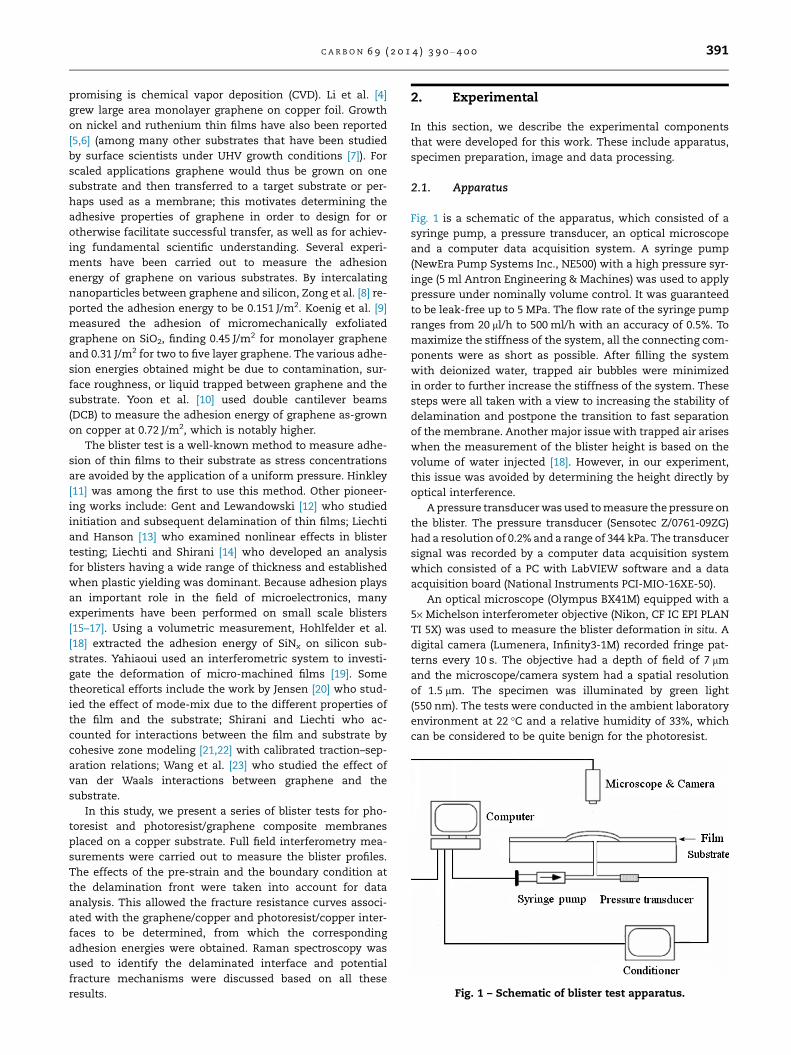
Fig. 1 – Schematic of blister test apparatus.
C A R B O N 6 9 ( 2 0 1 4 ) 3 9 0 – 4 0 0 391
promising is chemical vapor deposition (CVD). Li et al. [4]
grew large area monolayer graphene on copper foil. Growth
on nickel and ruthenium thin films have also been reported
[5,6] (among many other substrates that have been studied
by surface scientists under UHV growth conditions [7]). For
scaled applications graphene would thus be grown on one
substrate and then transferred to a target substrate or per-
haps used as a membrane; this motivates determining the
adhesive properties of graphene in order to design for or
otherwise facilitate successful transfer, as well as for achiev-
ing fundamental scientific understanding. Several experi-
ments have been carried out to measure the adhesion
energy of graphene on various substrates. By intercalating
nanoparticles between graphene and silicon, Zong et al. [8] re-
ported the adhesion energy to be 0.151 J/m2. Koenig et al. [9]
measured the adhesion of micromechanically exfoliated
graphene on SiO2, finding 0.45 J/m2 for monolayer graphene
and 0.31 J/m2 for two to five layer graphene. The various adhe-
sion energies obtained might be due to contamination, sur-
face roughness, or liquid trapped between graphene and the
substrate. Yoon et al. [10] used double cantilever beams
(DCB) to measure the adhesion energy of graphene as-grown
on copper at 0.72 J/m2, which is notably higher.
The blister test is a well-known method to measure adhe-
sion of thin films to their substrate as stress concentrations
are avoided by the application of a uniform pressure. Hinkley
[11] was among the first to use this method. Other pioneer-
ing works include: Gent and Lewandowski [12] who studied
initiation and subsequent delamination of thin films; Liechti
and Hanson [13] who examined nonlinear effects in blister
testing; Liechti and Shirani [14] who developed an analysis
for blisters having a wide range of thickness and established
when plastic yielding was dominant. Because adhesion plays
an important role in the field of microelectronics, many
experiments have been performed on small scale blisters
[15–17]. Using a volumetric measurement, Hohlfelder et al.
[18] extracted the adhesion energy of SiNx on silicon sub-
strates. Yahiaoui used an interferometric system to investi-
gate the deformation of micro-machined films [19]. Some
theoretical efforts include the work by Jensen [20] who stud-
ied the effect of mode-mix due to the different properties of
the film and the substrate; Shirani and Liechti who ac-
counted for interactions between the film and substrate by
cohesive zone modeling [21,22] with calibrated traction–sep-
aration relations; Wang et al. [23] who studied the effect of
van der Waals interactions between graphene and the
substrate.
In this study, we present a series of blister tests for pho-
toresist and photoresist/graphene composite membranes
placed on a copper substrate. Full field interferometry mea-
surements were carried out to measure the blister profiles.
The effects of the pre-strain and the boundary condition at
the delamination front were taken into account for data
analysis. This allowed the fracture resistance curves associ-
ated with the graphene/copper and photoresist/copper inter-
faces to be determined, from which the corresponding
adhesion energies were obtained. Raman spectroscopy was
used to identify the delaminated interface and potential
fracture mechanisms were discussed based on all these
results.
2. Experimental
In this section, we describe the experimental components
that were developed for this work. These include apparatus,
specimen preparation, image and data processing.
2.1. Apparatus
Fig. 1 is a schematic of the apparatus, which consisted of a
syringe pump, a pressure transducer, an optical microscope
and a computer data acquisition system. A syringe pump
(NewEra Pump Systems Inc., NE500) with a high pressure syr-
inge (5 ml Antron Engineering & Machines) was used to apply
pressure under nominally volume control. It was guaranteed
to be leak-free up to 5 MPa. The flow rate of the syringe pump
ranges from 20 ll/h to 500 ml/h with an accuracy of 0.5%. To
maximize the stiffness of the system, all the connecting com-
ponents were as short as possible. After filling the system
with deionized water, trapped air bubbles were minimized
in order to further increase the stiffness of the system. These
steps were all taken with a view to increasing the stability of
delamination and postpone the transition to fast separation
of the membrane. Another major issue with trapped air arises
when the measurement of the blister height is based on the
volume of water injected [18]. However, in our experiment,
this issue was avoided by determining the height directly by
optical interference.
A pressure transducer was used to measure the pressure on
the blister. The pressure transducer (Sensotec Z/0761-09ZG)
had a resolution of 0.2% and a range of 344 kPa. The transducer
signal was recorded by a computer data acquisition system
which consisted of a PC with LabVIEW software and a data
acquisition board (National Instruments PCI-MIO-16XE-50).
An optical microscope (Olympus BX41M) equipped with a
5· Michelson interferometer objective (Nikon, CF IC EPI PLAN
TI 5X) was used to measure the blister deformation in situ. A
digital camera (Lumenera, Infinity3-1M) recorded fringe pat-
terns every 10 s. The objective had a depth of field of 7 lm
and the microscope/camera system had a spatial resolution
of 1.5 lm. The specimen was illuminated by green light
(550 nm). The tests were conducted in the ambient laboratory
environment at 22 �C and a relative humidity of 33%, which
can be considered to be quite benign for the photoresist.

Fig. 2 – An AFM image of the topography of the copper
substrate. The RMS roughness is 4.7 nm over an area of
10 · 10 lm2. (A color version of this figure can be viewed
online.)
392 C A R B O N 6 9 ( 2 0 1 4 ) 3 9 0 – 4 0 0
2.2. Specimen preparation
In this study we were interested in determining the adhesion
of monolayer graphene that had been transferred to copper.
Accordingly, two types of specimens were considered. First
was a composite film of graphene coated with an epoxy pho-
toresist SU-8 2025 (MicroChem Corporation). The purpose of
the photoresist was to facilitate transfer of the graphene to
the copper and reinforce it during pressurization. For compar-
ison, the second specimen consisted of the same photoresist
on copper but without graphene.
The graphene that was used in this study was produced by
chemical vapor deposition (CVD), the details of which can be
found in [4,24]. The preparation of the photoresist started
with depositing a copper layer, roughly 100 nm thick, on a sil-
icon wafer using a Denton thermal evaporation system. The
operating pressure was approximately 10�6 Torr and the
deposition rate was 1 A/s. The photoresist was spun on top
of the copper layer at 2500 rpm for 35 s. The nominal thick-
ness of the photoresist was 33 lm, but this was measured in
each experiment using a profilometer (Dektak6M) with a ver-
tical range and resolution of 260 lm and 10 nm, respectively.
The sample was then soft-baked at 80 �C for 5 min. A razor
blade was used to cut grids of 1 · 1 cm on the photoresist
membrane. Then the assembly was submerged in an ammo-
nium persulfate solution (1.0 wt.%). The etchant flows
through the trenches to etch away the copper underneath
the photoresist. This process took 3–4 h. Finally, all the small
squares of photoresist were sonicated in deionized water. In
this way, optically flat photoresist films were obtained and
each square was used to produce a circular blister on copper.
The membranes consisting of graphene coated with photo-
resist were prepared in the same fashion except that a mono-
layer of CVD graphene was first transferred to the same copper
on silicon substrate referred to above [25,26]. The photoresist
was applied, cured and diced as above to produce squares of
graphene/photoresist. The etching process did not adversely
affect the adhesion of graphene to the photoresist.
The next step was to transfer the membrane over a
0.797 mm diameter drilled hole in a copper substrate to pro-
duce a free-standing window. The copper substrate was made
of 101 oxygen-free, high-conductivity (OFHC) copper (Trident,
Inc.). The surface of the substrate was first polished by a
range of sand papers, then by 3 lm, 1 lm, and 0.05 lm dia-
mond compound pastes, until it was mirror-like. Fig. 2 dis-
plays the topography of the copper substrate obtained by
atomic force microscopy (AFM). The root-mean-squared
(RMS) roughness was 4.7 nm over a 10 · 10 lm area approxi-
mately 0.15 mm from the edge of the hole. The RMS rough-
ness of three other areas nearby was 4.4, 4.1, and 3.9 nm.
Deionized water and acetone were applied to clean the sur-
face after polishing.
After the transfer, the specimen was baked at 135 �C for
15 min with pressure being applied via a small weight (approx-
imately 100 g). The weight prevented the heat flux from blow-
ing off the membrane, and also improved the contact between
the membrane and the substrate. The graphene with photore-
sist sample was prepared in a similar fashion, making sure
that the graphene side was in contact with the copper.
2.3. Blister deflection
After attaching the specimen to the pressure manifold with a
rubber O-ring seal, it was placed under the microscope (Fig. 1).
The distance between the objective and the specimen was
carefully adjusted so that fringe patterns were visible. At this
time the tilt of the reference mirror in the interference objec-
tive was also adjusted to establish proper alignment. At zero
pressure, the free-standing membrane was slack and drooped
below the copper substrate. The reason for this is not clear,
but one possibility is that gravity pulled the membrane down
while the epoxy was softening during the baking. Van der
Waals interactions between the films and side wall have been
noted for suspended graphene [9], but it is unlikely that they
were the cause of this phenomenon here due to greater thick-
ness of the films. Another possibility is that the application of
the weight at 135 �C to enhance contact following transfer re-
sulted in compressive residual strains during cool down. At
the same time, the glass transition temperature of the photo-
resist is 200 �C, making it unlikely that large viscoelastic ef-
fects could be responsible for this. Deflection profiles in this
initial state were obtained. In subsequent analysis of these
profiles, deflections were measured with respect to this initial
state. As the pressure increased due to the injection of deion-
ized water at a rate of 5 ml/h, a number of phenomena were
observed. More and more circular fringes were generated, as
the membrane was pressurized. Stable delamination of the
blister from the substrate initiated at a critical pressure
(approximately 75 kPa). In this regime, the delamination
could be arrested by stopping injection and the delamination
front remained quite circular. This is indicative of uniform
adhesion. The stable growth took place over about 50 lm
and was followed by unstable crack growth and blow-off of
the membrane. Before the blow-off, the delamination propa-
gated rapidly for approximately 2 s. Stopping injection did
not arrest the propagation. During the whole process, distin-
guishable fringes were apparent all over the blister, thereby
enabling whole field measurement of the blister deflections.
The membrane thickness was optimized to make sure that
the full range of deflections could be measured within the
C A R B O N 6 9 ( 2 0 1 4 ) 3 9 0 – 4 0 0 393
range of the pressure transducer. Membranes having a nom-
inal thickness of 33 lm achieved this objective.
Images of the fringe patterns were taken at 10 s intervals
using a time-lapse recording feature of the camera. The mem-
brane deflections were extracted from the centerlines of the
dark fringes. The associated image processing was accom-
plished with the ImageJ application. First, the image was di-
vided into approximately 30 square regions which were
chosen so that, within each region, the contrast of the dark
and bright fringes was roughly the same. Then the brightness
and contrast of each region was optimized until the ‘‘finding
local maximum’’ feature of ImageJ generated centerlines of
the dark fringes. Since the optimization of brightness and
contrast depended mainly on human judgment, which could
be a source of error, this operation was carried out several
times on the same photo to examine reproducibility. The dif-
ference was minimal. Finally, all the square regions were
assembled according to their locations in the original gray-
scale photo and the centerlines of the fringes were extracted
for subsequent transformation to the blister profiles.
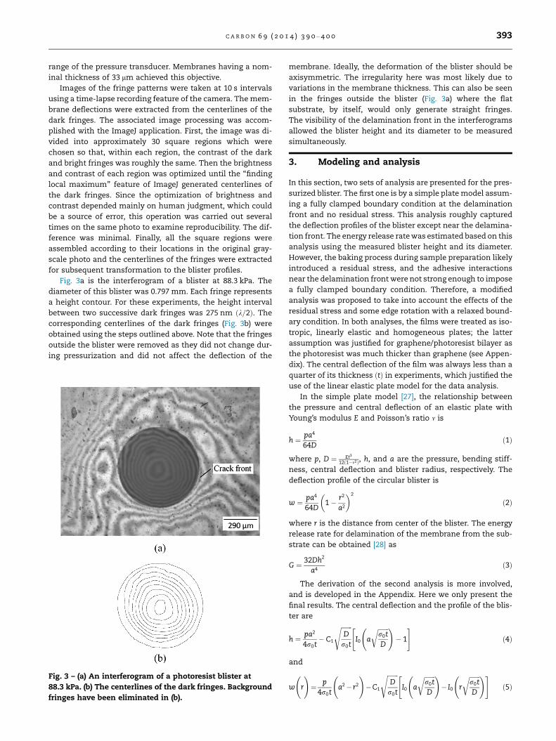
Fig. 3a is the interferogram of a blister at 88.3 kPa. The
diameter of this blister was 0.797 mm. Each fringe represents
a height contour. For these experiments, the height interval
between two successive dark fringes was 275 nm ðk=2Þ. The
corresponding centerlines of the dark fringes (Fig. 3b) were
obtained using the steps outlined above. Note that the fringes
outside the blister were removed as they did not change dur-
ing pressurization and did not affect the deflection of the
Fig. 3 – (a) An interferogram of a photoresist blister at
88.3 kPa. (b) The centerlines of the dark fringes. Background
fringes have been eliminated in (b).
membrane. Ideally, the deformation of the blister should be
axisymmetric. The irregularity here was most likely due to
variations in the membrane thickness. This can also be seen
in the fringes outside the blister (Fig. 3a) where the flat
substrate, by itself, would only generate straight fringes.
The visibility of the delamination front in the interferograms
allowed the blister height and its diameter to be measured
simultaneously.
3. Modeling and analysis
In this section, two sets of analysis are presented for the pres-
surized blister. The first one is by a simple plate model assum-
ing a fully clamped boundary condition at the delamination
front and no residual stress. This analysis roughly captured
the deflection profiles of the blister except near the delamina-
tion front. The energy release rate was estimated based on this
analysis using the measured blister height and its diameter.
However, the baking process during sample preparation likely
introduced a residual stress, and the adhesive interactions
near the delamination front were not strong enough to impose
a fully clamped boundary condition. Therefore, a modified
analysis was proposed to take into account the effects of the
residual stress and some edge rotation with a relaxed bound-
ary condition. In both analyses, the films were treated as iso-
tropic, linearly elastic and homogeneous plates; the latter
assumption was justified for graphene/photoresist bilayer as
the photoresist was much thicker than graphene (see Appen-
dix). The central deflection of the film was always less than a
quarter of its thickness ðtÞ in experiments, which justified the
use of the linear elastic plate model for the data analysis.
In the simple plate model [27], the relationship between
the pressure and central deflection of an elastic plate with
Young’s modulus E and Poisson’s ratio m is
h ¼ pa4
64Dð1Þ
where p, D ¼ Et3
12ð1�m2Þ, h, and a are the pressure, bending stiff-
ness, central deflection and blister radius, respectively. The
deflection profile of the circular blister is
w ¼ pa4
64D1� r2
a2
� �2
ð2Þ
where r is the distance from center of the blister. The energy
release rate for delamination of the membrane from the sub-
strate can be obtained [28] as
G ¼ 32Dh2
a4ð3Þ
The derivation of the second analysis is more involved,
and is developed in the Appendix. Here we only present the
final results. The central deflection and the profile of the blis-
ter are
h ¼ pa2
4r0t� C1
ffiffiffiffiffiffiffiDr0t
sI0 a
ffiffiffiffiffiffiffir0tD
r !� 1
" #ð4Þ
and
w
r
!¼ p
4r0t
a2�r2
!�C1
ffiffiffiffiffiffiffiDr0t
sI0 a
ffiffiffiffiffiffiffir0tD
r !� I0 r
ffiffiffiffiffiffiffir0tD
r !" #ð5Þ
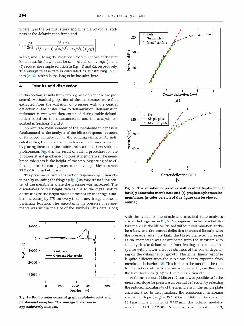
Fig. 5 – The variation of pressure with central displacement
for (a) photoresist membrane and (b) graphene/photoresist
membrane. (A color version of this figure can be viewed
online.)
394 C A R B O N 6 9 ( 2 0 1 4 ) 3 9 0 – 4 0 0
where r0 is the residual stress and Ks is the rotational stiff-
ness at the delamination front, and
C1 ¼pa
2r0t
KsaD þ mþ 1
KsaD þ m� 1� �
I1 affiffiffiffiffir0tD
q� �þ a
ffiffiffiffiffir0tD
qI0 a
ffiffiffiffiffir0tD
q� �264
375 ð6Þ
with I0 and I1 being the modified Bessel functions of the first
kind. It can be shown that, for Ks !1 and r0 ! 0, Eqs. (4) and
(5) recover the simple solution in Eqs. (1) and (2), respectively.
The energy release rate is calculated by substituting (A.15)
into (A.16), which is too long to be included here.
4. Results and discussion
In this section, results from two regimes of response are pre-
sented. Mechanical properties of the membranes were first
extracted from the variation of pressure with the central
deflection of the blister prior to delamination. Delamination
resistance curves were then extracted during stable delami-
nation based on the measurements and the analysis de-
scribed in Sections 2 and 3.
An accurate measurement of the membrane thickness is
fundamental to the analysis of the blister response, because
of its cubed contribution to the bending stiffness. As indi-
cated earlier, the thickness of each membrane was measured
by placing them on a glass slide and scanning them with the
profilometer. Fig. 4 is the result of such a procedure for the
photoresist and graphene/photoresist membranes. The mem-
brane thickness is the height of the step. Neglecting edge ef-
fects due to the cutting process, the average thickness was
33.2 ± 0.6 lm in both cases.
The pressure vs. central deflection response (Fig. 5) was ob-
tained by counting the fringes (Fig. 3) as they crossed the cen-
ter of the membrane while the pressure was increased. The
discreteness of the height data is due to the digital nature
of the fringes; the height was determined by the fringe num-
ber, increasing by 275 nm every time a new fringe crosses a
particular location. The uncertainty in pressure measure-
ments was within the size of the symbols. This data, along
Fig. 4 – Profilometer scans of graphene/photoresist and
photoresist samples. The average thickness is
approximately 33.2 lm.
with the results of the simple and modified plate analyses
are plotted together in Fig. 5. Two regimes can be detected. Be-
fore the kink, the blister bulged without delamination at the
interface, and the central deflection increased linearly with
the pressure. After the kink, the blister diameter increased
as the membrane was delaminated from the substrate with
a nearly circular delamination front, leading to a nonlinear re-
sponse with a lower effective stiffness of the blister depend-
ing on the delamination growth. The initial linear response
is quite different from the cubic one that is expected from
membrane behavior [18]. This is due to the fact that the cen-
tral deflections of the blister were considerably smaller than
the film thickness ½ðt=hÞ2 � 1� in our experiments.
With the measured blister radiusa, it was possible to fit the
measured slope for pressure vs. central deflection by selecting
the reduced modulus E1�m2 of the membrane in the simple plate
analysis. Prior to delamination, the photoresist membrane
yielded a slope ph ¼ 64D
a4 ¼ 35:2 GPa/m. With a thickness of
32.4 lm and a diameter of 0.797 mm, the reduced modulus
was then 4.89 ± 0.12 GPa. Assuming Poisson’s ratio of 0.3,

Fig. 7 – Profiles of a photoresist blister under varying
pressures. Points are measured data. Lines are calculated
from (a) simple and (b) modified plate models with
Ks ¼ 0:32 N and e0 ¼ 0:2%. (A color version of this figure can
be viewed online.)
C A R B O N 6 9 ( 2 0 1 4 ) 3 9 0 – 4 0 0 395
the Young’s modulus of the photoresist is 4.45 ± 0.11 GPa. This
result is in good agreement with existing data for similar pho-
toresists [29,30]. Carrying out the same analysis on the mem-
brane with graphene and photoresist yielded a reduced
modulus of 4.54 GPa. The similarity of the values of reduced
moduli for the two cases indicates that the presence of graph-
ene did not change the stiffness of the membrane noticeably,
which is not surprising since the in-plane stiffness of the
photoresist membrane was about 400 times of the graphene
(i.e., Ept >> Eg2D). For both types of the blister, the simple plate
model agrees well with the measured data up until the last
few points, where the model overestimates the deflection.
The reason for the discrepancy is not clear, but the blister
did become slightly oval with a minor to major axis ratio less
than 1 but always greater than 0.9. Although the average ra-
dius was used in the modeling, there is still room for uncer-
tainty as the radius effects height to the fourth power.
In preparation for obtaining bulge profiles at various pres-
sure levels, the centerlines of the dark fringes were converted
to three dimensional surfaces (Fig. 6) by interpolating be-
tween centerlines using the CFTOOL routine in MATLAB. Once
these had been obtained, the deflected surface at zero pres-
sure was taken to be the reference state and was subtracted
from the surface topographies at all subsequent pressure lev-
els to reveal the corresponding deflection. For comparison, ra-
dial profiles predicted from the simple and modified plate
models were plotted as a function of pressure level (Fig. 7).
The lines in Fig. 7a represent Eq. (2), which was developed un-
der zero residual stress and a fully clamped boundary condi-
tion. However, in the experiment, residual stress was present
and there was a nonzero deflection slope dwdr ¼ h� �
at r ¼ a.
These resulted in the discrepancy between measured and
predicted deflections from the simple plate model, especially
near the delamination front. The modified plate model was
proposed to resolve these issues. By choosing the appropriate
combination of residual stress and rotational stiffness
through a parametric study, a better fit to the measured pro-
files was achieved (Fig. 7b). Using the same parameters, the
center deflection vs. pressure response by the modified plate
model shows no significant difference from the simple plate
model (Fig. 5).
Examples of the delamination growth histories of speci-
mens with photoresist and copper and photoresist, graphene
and copper are shown in Fig. 8a and b, respectively. It can be
seen that delamination accelerated gradually until the growth
became unstable and the films blew off. The filled points in
each case corresponded to steady-state behavior in the
Fig. 6 – 3D profile of a blister at a pressure of 115 kPa. The
deformation is with respect to the initial shape, a concave
surface. (A color version of this figure can be viewed online.)
resistance curves (Fig. 9). In this regime, the delamination
rates were 0.7 and 0.4 lm/s, respectively, for the photoresist/
copper and graphene/copper interfaces.
The deflection profiles (Fig. 7) and the delamination
growth data (Fig. 8) were the basis for determining delamina-
tion resistance curves (Fig. 9) that represented the adhesive
interactions of the photoresist/copper (Fig. 9a and c) and
graphene/copper (Fig. 9b and d) interfaces. In cases where
an interface is completely brittle, its resistance curve is a step
function which initiates at the origin and jumps to the tough-
ness Cc of the interface. In other words, as soon as the energy
release rate being provided by the pressure reaches Cc, the
crack propagates and the energy release rate remains con-
stant (G ¼ Cc). For realistic interfaces, the step function is re-
placed by a gradually increasing resistance to delamination,
which eventually reaches a steady state value Css, as the
delamination proceeds with a constant energy release rate
ðG ¼ CssÞ. In the simple plate model, the energy release rate
is calculated from Eq. (3), using the measured blister radius
a and central deflection h along with the bending stiffness D
obtained from the slope of the pressure vs. central deflection

Fig. 8 – Crack growth histories for (a) photoresist/copper and
(b) graphene/copper.
396 C A R B O N 6 9 ( 2 0 1 4 ) 3 9 0 – 4 0 0
response (Fig. 5). Fig. 9a and b are the resistance curves for
three photoresist/copper interfaces and four graphene/copper
interfaces, respectively, each from different specimens. In all
the cases, the resistance curves rose quite sharply from the
initiation toughness ðG ¼ C0Þ before reaching a steady state
regime ðG ¼ CssÞ, which then transitioned to unstable growth,
represented by the last data point. This was taken to be the
interfacial toughness of each particular specimen. The initia-
tion toughness ðC0Þ of each interface was similar, ranging
from 0.03 to 0.07 J/m2 for the photoresist/copper interface
and 0.02 to 0.08 J/m2 for the graphene/copper interface. The
corresponding average values for the steady state toughness
ðCssÞ obtained from all the specimens were 0.264 ± 0.013 and
0.341 ± 0.024 J/m2, respectively, which are lower than the val-
ues for adhesive energy reported previously [9,29]. The blister
was blown off shortly after the plateau was reached, most
likely due to some compliance in the pressurization system.
The amount of delamination growth that was required to
achieve a steady state was approximately 50 lm in both cases.
The total growth was approximately 100 lm before the blister
became unstable.
Using the parameters determined in Fig. 7b, the energy re-
lease rate was also determined from the modified plate model
with the effects of residual stress and rotational stiffness at
the delamination front (see Appendix). Fig. 9c and d compare
the resistance curves obtained from the modified plate model
with those from the simple plate model, using one of the data
sets for each interface. The two models yielded similar trends
but the modified plate model resulted in higher energy re-
lease rates. The difference was largest just prior to onset of
unstable growth. This is because the energy release rate from
the modified plate model was calculated using the measured
pressure and blister radius, as opposed to blister height and
radius for the simple plate model. Since this model overesti-
mated the blister height in this regime (Fig. 5), the calculated
energy release rates using the measured pressure are higher
than those using the measured height, which made the pla-
teau in the resistance curve (Fig. 9c and d) disappear. Taking
the last data point of the resistance curve as the closest
approximation of the steady-state toughness, the modified
plate model yielded toughness values of 0.465 ± 0.008 and
0.484 ± 0.007 J/m2 for photoresist/copper and graphene/cop-
per interfaces, respectively. The uncertainty was estimated
by running the analysis with propagation of uncertainties in
pressure, modulus and blister radius. As might be expected,
these values of toughness are lower than the toughness of
graphene being separated from seed copper [10]. They are in
the same range as the values for graphene transferred to sil-
icon [9]. Koenig et al. [9] noted that the measured adhesion
energy of multi-layer graphene to silicon was less than that
of monolayer graphene, likely due to a transition from confor-
mal to non-conformal morphologies associated with the lar-
ger bending modulus of multilayer graphene [31]. Similar
effects can be expected when graphene is backed by the much
stiffer (based on tensile modulus times layer thickness) pho-
toresist layer employed in this study. Moreover, it is interest-
ing to note that, based on the fully clamped condition, the
adhesive toughness of graphene transferred to copper was
about 70 mJ/m2 higher than that for photoresist alone. This
suggests that the presence of graphene enhances the adhe-
sion energy (in comparison to photoresist alone), which
may be attributed to the close packing of carbon atoms in
graphene. As noted before [32], the adhesion energy of van
der Waals interactions is proportional to the number density
of the atoms. At the same time, the modified analysis sug-
gests that there is no significant difference between the adhe-
sive toughness values of the two interfaces, which could
suggest that there was no influence from the graphene. These
issues clearly require further study. Finally, it should be noted
that the fracture mode-mix (ratio of shear to tension) of the
blisters in the present study is between �45� and �65� [20].
If there is any mode-mix dependence [33] for the interfacial
fracture between graphene and copper, then further experi-
ments would be required.
After the graphene/photoresist membrane had been
blown off from the copper substrate, the graphene side of
the membrane was inspected by Raman spectroscopy. This
was to verify that the delamination occurred at graphene/
copper interface rather than graphene/photoresist interface.
The presence of graphene on the photoresist film before and
after the blister test is indicated (Fig. 10) by the G and 2D
peaks at 1583 and 2721 cm�1, respectively. The D peak region
(1350–1380 cm�1), which is used to ascertain the quality of

Fig. 9 – Resistance curves for (a) photoresist/copper and (b) graphene/copper interfaces based on the measurements and the
simple plate model. A comparison of resistance curves from simple and modified plate models for (c) photoresist/copper and
(d) graphene/copper interfaces, respectively. (A color version of this figure can be viewed online.)
Fig. 10 – Raman spectra of the graphene side of the
photoresist membrane before and after a blister test. (A
color version of this figure can be viewed online.)
C A R B O N 6 9 ( 2 0 1 4 ) 3 9 0 – 4 0 0 397
graphene, was present but was masked by contributions
from the photoresist itself making it impossible to make a
definitive assessment. The ratio of the peak intensities
ðIG=I2DÞ is 1:3 for high quality monolayer graphene [34] on
silicon. The ratio obtained here was 1:12, which was an aver-
age of three spectra from two different specimens; each
spectrum was itself an average of three runs. The lower
intensity ratio is likely due to background noise produced
by the photoresist, which is an epoxy that also contains
sp2 carbon bonding. Another possibility is contamination
during the graphene transfer, most likely from residue of
the PMMA [25] that was used in the transfer of the graphene
to the copper substrate. This could indicate that the acetone
did not completely remove the PMMA. Subsequent heating
of the PMMA was not feasible in this case due to the poten-
tial for oxidization of the copper. Nonetheless, the intensity
ratio of the G band to 2D band and the minimal D band
indicate that the graphene was separated from the copper
substrate with minimal defects.

398 C A R B O N 6 9 ( 2 0 1 4 ) 3 9 0 – 4 0 0
5. Conclusions
This paper describes the development of a blister test for
characterizing the interfacial adhesion of graphene that had
been transferred to a polished copper surface over larger
areas than have been previously considered. SU-8 2025 photo-
resist served as a backing layer, and its adhesion to copper
was also studied for comparison. A simple plate model with
zero residual stress and a fully clamped boundary was
adopted to extract the mechanical behavior of each mem-
brane and the interfacial toughness associated with their
adhesion to copper. The blister profiles predicted by the
simple model did not correspond to the measurements
everywhere, with relatively large discrepancies near the
delamination front. A modified plate model resolved this is-
sue by accounting for the presence of residual stress and rota-
tional stiffness at the delamination front. As a result, there
was a difference in the calculated energy release rates for
the resistance curves. The steady-state toughness or adhe-
sion energy was obtained from the resistance curves; simple
plate model yielded 0.264 ± 0.013 J/m2 and 0.341 ± 0.024 J/m2
for photoresist/copper and graphene/copper interfaces,
respectively, whereas modified plate model yielded values of
0.44 J/m2 and 0.51 J/m2, emphasizing the need to account for
residual stress effects and the rotational stiffness of the
delamination front when relatively weak interactions are at
play. The higher toughness values obtained by the modified
analysis are in closer agreement with measurements of
graphene interactions, albeit with other substrates. Raman
spectroscopy was carried out to examine the delamination
path for the copper/graphene/photoresist specimens, which
confirmed delamination between copper and graphene over
a large area.
Acknowledgements
The authors gratefully acknowledge partial financial sup-
port of this work by the National Science Foundation
through Grant No. CMMI-1130261. This work is also based
upon work supported in part by the National Science Foun-
dation under Cooperative Agreement No. EEC-1160494. Any
opinions, findings and conclusions or recommendations ex-
pressed in this material are those of the author(s) and do
not necessarily reflect the views of the National Science
Foundation.
Appendix A
Prior to pressurization, the strain components of the mem-
brane are:
er ¼ e0; eh ¼ e0 and erh ¼ 0; ðA:1Þ
where e0 is the pre-strain. The radial and circumferential
membrane forces are:
Nr ¼ Nh ¼ Se0; ðA:2Þ
where S is the biaxial in-plane stiffness of the membrane. The
average residual stress is then r0 ¼ Se0=t, where t is the mem-
brane thickness.
Upon pressurization, the deflection profile of the circular
blister is assumed to be axi-symmetric with w ¼ wðrÞ. The
curvature components are
jr ¼d2wdr2
; jh ¼1r
dwdr
and jrh ¼ 0: ðA:3Þ
The corresponding bending moments are
Mr ¼ Dd2wdr2þ m
rdwdr
!andMh ¼ D m
d2wdr2þ 1
rdwdr
!ðA:4Þ
where D is the bending stiffness and m is Poisson’s ratio. Mo-
ment equilibrium yields the equation for the deflection of
the membrane:
Dd3wdr3þ 1
rd2wdr2� 1
r2
dwdr
!� r0t
dwdr¼ 1
r
Z r
0
qrdr ðA:5Þ
where q is the lateral loading intensity. In the present study,
the loading was a uniform pressure q ¼ p and the right hand
side reduces to pr=2.
Because of symmetry, the boundary condition at center
(r ¼ 0) is h ¼ dwdr ¼ 0. At the delamination front r ¼ a, the deflec-
tion w ¼ 0. In order to account for the possibility of rotation at
the delamination front due to the nature of the interactions
between the film and substrate, a spring-like boundary condi-
tion is assumed:
Mr ¼ Dd2wdr2þ m
rdwdr
!¼ �Ks
dwdr
ðA:6Þ
where Ks is the rotational stiffness of the delamination front.
This indicates that, at the boundary (r ¼ a), the radial moment
is proportional to angle of rotation. When Ks ¼ 0, the bound-
ary condition becomes a simply-supported one while the
fully-clamped condition corresponds to Ks !1.
The solution to Eq. (A.5) can be developed by rewriting it in
terms of the rotation h ¼ dwdr as
d2hdr2þ 1
rdhdr� 1
r2þ r0t
D
� �h ¼ pr
2DðA:7Þ
The angle of rotation is then obtained as
hðrÞ ¼ C1I1 r
ffiffiffiffiffiffiffir0tD
r !þ C2K1 r
ffiffiffiffiffiffiffir0tD
r !� pr
2r0tðA:8Þ
where I1ðxÞ and K1ðxÞ are modified Bessel functions of the first
and second kinds, respectively. Applying the boundary condi-
tion at r = 0 leads to C2 ¼ 0, and the condition (A.6) at r = a
yields
C1 ¼pa
2r0t
KsaD þ mþ 1
KsaD þ m� 1� �
I1 affiffiffiffiffir0tD
q� �þ a
ffiffiffiffiffir0tD
qI0 a
ffiffiffiffiffir0tD
q� �264
375 ðA:9Þ
The deflection is then obtained by integrating the angle of
rotation so that
w¼ p4r0t
a2�r2
!�C1
ffiffiffiffiffiffiffiDr0t
sI0 a
ffiffiffiffiffiffiffir0tD
r !� I0 r
ffiffiffiffiffiffiffir0tD
r !" #: ðA:10Þ
The central deflection is thus
h ¼ pa2
4r0t� C1
ffiffiffiffiffiffiffiDr0t
sI0 a
ffiffiffiffiffiffiffir0tD
r !� 1
" #ðA:11Þ

C A R B O N 6 9 ( 2 0 1 4 ) 3 9 0 – 4 0 0 399
To obtain the energy release rate for advancing the delam-
ination front, we calculate the total potential energy as fol-
lows. The strain energy of the membrane consists of two
parts: one due to bending and the other one due to stretching.
With the biaxial residual stress, the elastic stretching energy
per unit area is approximately
UsðrÞ ¼r0t2
dwdr
� �2
ðA:12Þ
The elastic bending energy per unit area is
UbðrÞ ¼D2
d2wdr2
!2
þ 1r2
dwdr
� �2
þ 2vr
dwdr
d2wdr2
0@
1A ðA:13Þ
In addition, the potential energy due to the rotational
spring-like condition at the delamination front (per unit
length) is
Uk ¼12
Ksdwdr
� �2r¼a
ðA:14Þ
The total potential energy of the pressurized blister is
then
Pða;pÞ ¼2pR a
0 ½UsðrÞþUbðrÞ�rdrþ2paUk�2ppR a
0 wðrÞrdr
¼�ppR a
0 wðrÞrdr
¼�pp2a4
16r0t�pDp2a2
2ðr0tÞ2KsaD þmþ1� �
I1 affiffiffiffiffir0tD
q� �� a
2
ffiffiffiffiffir0tD
qI0 a
ffiffiffiffiffir0tD
q� �h iKsaD þm�1� �
I1 affiffiffiffiffir0tD
q� �þa
ffiffiffiffiffir0tD
qI0 a
ffiffiffiffiffir0tD
q� �ðA:15Þ
The energy release rate for delamination is obtained as a
function of the blister radius and the pressure as
Gða;pÞ ¼ � 12pa
@Pða;pÞ@a
� �ðA:16Þ
For fully clamped boundary condition with Ks !1, the po-
tential energy becomes
Pða;pÞ ¼ �pp2a4
16r0t� pDp2a2
2ðr0tÞ21�
affiffiffiffiffir0tD
qI0 a
ffiffiffiffiffir0tD
q� �2I1 a
ffiffiffiffiffir0tD
q� �264
375: ðA:17Þ
Further when r0 ! 0, the potential energy reduces to
Pða;pÞ ¼ �pp2a6
384D: ðA:18Þ
Substitution of (A.18) into (A.16) recovers the simple solu-
tion in Eq. (3) for the energy release rate with zero residual
stress and fully clamped boundary condition.
The membrane with photoresist and graphene can be con-
sidered as a bilayer composite plate of total thickness t. The
effective biaxial in-plane stiffness of the composite is
S ¼ 11� v
Eptþ Eg2D
� �¼ Ept
1� v1þ kð Þ ðA:19Þ
where Ep is Young’s modulus of the photoresist, Eg2D is the
two-dimensional Young’s modulus of graphene [4], and
k ¼ Eg2D
Ept. Because the graphene monolayer is much thinner
than the photoresist, the overall Poisson’s ratio is approxi-
mately that of the photoresist alone. Similarly, the effective
bending stiffness of the composite membrane is
approximately
D ¼ Ept3
12ð1� m2Þ1þ 4k1þ k
: ðA:20Þ
For our experiments, Ept >> Eg2D and k! 0. Hence, we have
S � Ept1�v and D � Ept3
12ð1�m2Þ, implying that we can use the in-plane
and bending stiffness of the photoresist alone for the com-
posite membrane.
R E F E R E N C E S
[1] Lee C, Wei XD, Kysar JW, Hone J. Measurement of the elasticproperties and intrinsic strength of monolayer graphene.Science 2008;321(5887):385–8.
[2] Lin YM, Dimitrakopoulos C, Jenkins KA, Farmer DB, Chiu HY,Grill A, et al. 100 GHz transistors from wafer-scale epitaxialgraphene. Science 2010;327(5966). 662-662.
[3] Bae S, Kim H, Lee Y, Xu XF, Park JS, Zheng Y, et al. Roll-to-rollproduction of 30 in. graphene films for transparentelectrodes. Nat Nanotechnol 2010;5(8):574–8.
[4] Li XS, Cai WW, An JH, Kim S, Nah J, Yang DX, et al. Large-areasynthesis of high-quality and uniform graphene films oncopper foils. Science 2009;324(5932):1312–4.
[5] Kim KS, Zhao Y, Jang H, Lee SY, Kim JM, Kim KS, et al. Large-scale pattern growth of graphene films for stretchabletransparent electrodes. Nature 2009;457(7230):706–10.
[6] Sutter PW, Flege JI, Sutter EA. Epitaxial graphene onruthenium. Nat Mater 2008;7(5):406–11.
[7] Batzill M. The surface science of graphene: metal interfaces,CVD synthesis, nanoribbons, chemical modifications, anddefects. Surf Sci Rep 2012;67(3–4):83–115.
[8] Zong Z, Chen CL, Dokmeci MR, Wan KT. Direct measurementof graphene adhesion on silicon surface by intercalation ofnanoparticles. J Appl Phys 2010;107(2):026104.
[9] Koenig SP, Boddeti NG, Dunn ML, Bunch JS. Ultrastrongadhesion of graphene membranes. Nat Nanotechnol2011;6:543–6.
[10] Yoon T, Shin WC, Kim TY, Mun JH, Kim TS, Cho BJ. Directmeasurement of adhesion energy of monolayer graphene as-grown on copper and its application to renewable transferprocess. Nano Lett 2012;12(3):1448–52.
[11] Hinkley JA. A blister test for adhesion of polymer films toSiO2. J Adhes 1983;16:115–25.
[12] Gent AN, Lewandowski LH. Blow-off pressures for adheringlayers. J Appl Polym Sci 1987;33:1567–77.
[13] Liechti KM, Hanson E. Nonlinear effects in mixed-modedelaminations. Int J Fract 1988;36:199–217.
[14] Liechti KM, Shirani A. Large scale yielding in blisterspecimens. Int J Fract 1994;67:21–36.
[15] Allen MG, Mehregany M, Howe RT, Senturia SD.Microfabricated structures for the in situ measurement ofresidual stress, young’s modulus, and ultimate strain of thinfilms. Appl Phys Lett 1987;51:241–3.
[16] Allen MG, Senturia SD. Analysis of critical debondingpressures of stressed thin films in the blister test. J Adhes1988;25:303–15.
[17] Allen MG, Senturia SD. Application of the island blister testfor thin film adhesion measurement. J Adhes 1989;29:219–31.
[18] Hohlfelder RJ, Luo HH, Vlassak JJ, Chidsey CED, Nix WD.Measuring interfacial fracture toughness with the blister test.Mater Res Soc Symp Proc 1997;436:115–20.
[19] Yahiaoui R, Danaie K, Petitgrand S, Bosseboeuf A. Anautomated interferometric system for bulge and blister testmeasurements of micromachined membranes. Proc SPIE2001;4400:160–9.

400 C A R B O N 6 9 ( 2 0 1 4 ) 3 9 0 – 4 0 0
[20] Jensen HM. Analysis of mode mixity in blister tests. Int J Fract1998;94:79–88.
[21] Liechti KM, Shirani A, Dillingham RG, Boerio FJ, Weaver SM.Cohesive zone models of polyimide/aluminum interphases. JAdhes 2000;73:259–97.
[22] Shirani A, Liechti KM. A calibrated fracture process zonemodel for thin film blistering. Int J Fract 1998;93(1–4):281–314.
[23] Wang P, Gao W, Cao Z, Liechti KM, Huang R. Numericalanalysis of circular graphene bubbles. J Appl Mech2013;80:040905.
[24] Tao L, Lee J, Chou H, Holt M, Ruoff RS, Akinwande D.Synthesis of high quality monolayer graphene at reducedtemperature on hydrogen-enriched evaporated copper (111)films. ACS Nano 2012;6(3):2319–25.
[25] Li XS, Zhu YW, Cai WW, Borysiak M, Han BY, Chen D, et al.Transfer of large-area graphene films for high-performancetransparent conductive electrodes. Nano Lett2009;9(12):4359–63.
[26] Suk JW, Kitt A, Magnuson CW, Hao Y, Ahmed S, An J, et al.Transfer of CVD-grown monolayer graphene onto arbitrarysubstrates. ACS Nano 2011;5(9):6916–24.
[27] Timoshenko SP, Woinowsky-Krieger S. Theory of plates andshells. 2nd ed. New York: McGraw-Hill; 1987. p. 93.
[28] Kanninen MF, Popelar CH. Advanced fracturemechanics. Oxford, UK: Oxford University Press; 1985. p. 375.
[29] Goyal S, Srinivasan K, Subbarayan G, Siegmund T. A non-contact, thermally-driven buckling delamination test tomeasure interfacial fracture toughness of thin film systems.Thin Solid Films 2010;518(8):2056–64.
[30] Al-Halhouji AT, Kampen I, Krah T, Buettgenbach S.Nanoindentation testing of SU-8 photoresist mechanicalproperties. Microelectron Eng 2008;85(5–6):942–4.
[31] Gao W, Huang R. Effect of surface roughness on adhesion ofgraphene membranes. J Phys D Appl Phys 2011;44(45):452001.
[32] Aitken ZH, Huang R. Effects of mismatch strain and substratesurface corrugation on morphology of supported monolayergraphene. J Appl Phys 2010;107:123531.
[33] Chai YS, Liechti KM. Asymmetric shielding in interfacialfracture under in-plane shear. J Appl Mech 1992;59:295–304.
[34] Ferrari AC, Meyer JC, Scardaci V, Casiraghi C, Lazzeri M, MauriF, et al. Raman spectrum of graphene and graphene layers.Phys Rev Lett 2006;97(18):187401.