a bit-serial viterbi processor
TRANSCRIPT

A BIT-SERIAL VITERBI PROCESSOR
A Thesis
Submitted to the Faculty of Graduate Studies and Research
in Partial Fulfillment of the Requirements
for the Degree of
Master of Science
in the Department of Electrical Engineering
University of Saskatchewan
by
Michael Arthur Bree
Saskatoon, Saskatchewan
DECEMBER, 1988
Copyright (c) 1988 M. A. Bree
ii
Copyright
The author has agreed that the Library, University of Saskatchewan, shall make this
thesis freely available for inspection. Moreover, the author has agreed that permission for
extensive copying of this thesis for scholarly purposes may be granted by the professor or
professors who supervised the thesis work recorded herein or, in their absence, by the
Head of the Department or Dean of the College in which this thesis work was done. It is
understood that due recognition will be given to the author of this thesis and to the
University of Saskatchewan in any use of the material in this thesis. Copying or
publication or any other use of the thesis for financial gain without approval by the
University of Saskatchewan and the author's written permission is prohibited.
Requests for permission to copy or to make other use of the material in this thesis in
whole or in part should be addressed to:
Head of the Department of Electrical Engineering,
University of Saskatchewan,
SASKATOON, Canada.

iii
Acknowledgements
The author wishes to thank Professor D. E. Dodds for his supervision, guidance and
encouragement during the course of this work, and for suggesting the original idea. He
also thanks his wife, Terry, and daughter, Sarah, for their patience and encouragement.
The author gratefully acknowledges the assistance of Professor R. J. Bolton during the
VLSI portion of this work, and the assistance of Brian Wirth during the circuit layout.
Financial assistance, in the form of an Industrial Postgraduate Scholarship jointly
funded by Develcon Electronics and the Natural Sciences and Engineering Research
Council, and in the form of a University of Saskatchewan Graduate Scholarship is
gratefully acknowledged.
Layouts and simulations for the VLSI portion of this work were carried out on
equipment supplied by the Canadian Microelectronics Corporation and the integrated
circuits were fabricated by Northern Telecom.

iv
UNIVERSITY OF SASKATCHEWAN
Electrical Engineering Abstract 88A300
A BIT-SERIAL VITERBI PROCESSOR
Student: M. A. Bree
Supervisor: D. E. Dodds
M.Sc. Thesis Presented to the College of Graduate Studies
December 1988
Abstract
The Viterbi algorithm is used for Forward Error Control (FEe) in systems such as
satellite communication. Smaller networks are now utilizing satellite technology, which
has created a demand for low cost, moderate speed Viterbi Decoders.
Many low cost VLSI Viterbi decoders use bit parallel, sequential node processing
techniques. In this thesis, bit-serial techniques are applied which reduce circuit size and
allow for a parallel node processing implementation. The use of bit-serial communication
paths between circuits also reduces wiring area requirements when compared with bit
parallel busses. Off-chip wiring of the processing trellis allows multiple chips to be
cascaded, thus increasing decoder constraint length and bit-error correction capability. A
technique is presented which pairs the node processing circuits and further reduces the
number of I/O pins and wires.
VLSI chips were designed using the QUISC silicon compiler and associated standard
cell library. A single chip can implement constraint length K=4 and will support eight level
soft decision and code rates of R=1/2 andR=1/3. A Viterbi algorithm simulator, VSIM,
was written to aid in the design and debugging of the chip. The simulator can also be used
to predict the performance of various decoder configurations of cascaded chips. Fabricated
chips were found to operate as expected at decoded data rates up to 287 kbps. Simulations
indicate coding gains ranging from 3.8 dB to 5.2 dB at a decoded bit-error-rate of 10-5•

v
Table Of Contents
Copyright ii
Acknowledgements iii
Abstract iv
Table of Contents v
List of Figures viii
List of Tables x
List of Abbreviations xi
1. INTRODUCTION 1
1.1 Background 1
1.2 Project Objectives 3
1.3 Thesis Outline 3
2. THE VITERBI ALGORITHM 4
2.1 Coding in Digital Communication Systems 4
2.2 Coding Techniques 10
2.2.1 Block codes 10
2.2.2 Convolutional codes 11
2.3 Convolutional Decoding 15
2.3.1 Sequential decoding 15
2.3.2 Threshold decoding 18
2.3.3 Viterbi decoding 20
2.4 Viterbi Decoder Architectures and Implementations 26
3. BIT-SERIAL VITERBI PROCESSOR SYSTEM LEVEL DESIGN 33
3.1 Conventional Design Techniques 33
3.2 The Bit-Serial Approach 34
3.3 Trellis Modeling 35
3.4 External Wiring 36

vi
3.4.1 Cascadability 38
3.4.2 Multiple code support 39
3.5 Pairing Node Processor Circuits 40
3.6 Viterbi Processor System Architecture 42
4. VITERBI PROCESSOR CIRCUIT LEVEL DESIGN 44
4.1 Branch Metric Circuit Architecture 44
4.1.1 Branch metric circuit design 47
4.1.2 Branch metric circuit operation 51
4.1.3 Bit metric generator circuit 52
4.1.4 Bit metric routing circuit 54
4.1.5 Branch metric calculator circuit 56
4.1.6 Branch metric routing circuit 57
4.2 Node Processor Architecture 59
4.2.1 Add~compare-select operation 60
4.2.2 Path history update 65
4.3 Output Circuit Architecture 68
4.3.1 Decoded output data detennination 68
4.3.2 Normalization circuit 72
4.4 Control Circuit Architecture 73
4.4.1 Control and co-ordination 75
4.4.2 Pipelined operation 76
4.4.3 Interface control 77
s. VLSI IMPLEMENTATION AND TESTING 78
5.1 Development Environment 79
5.2 Viterbi Processor VLSI Layout 81
5.3 VLSI Chip Test Results 84
5.3.1 Detailed SKVPB testing 84
6. ANALYSIS OF PROPOSED VITERBI DECODING SYSTEM 91
6.1 VSIM Viterbi Decoder Coding Gain Estimates 91
6.2 Proposed Viterbi Decoder Architecture 95
6.2.1 Majority vote and normalization 98
6.2.2 Demodulation and synchronization 100
6.2.3 Lost synchronization detection 100

vii
7. CONCLUSIONS 105
7.1 Summary of Viterbi Processor Features 105
7.2 Suggestions for Future Study 106
REFERENCES 109
APPENDIX A: VHDL LISTINGS 112
APPENDIX B: VSIM VITERBI ALGORITHM SIMULATOR 132
B.l VSIM Program Structure 132
B.2 VSIM Program Operation 135
B.3 VSIM Commands 136

Fig. 2.1:
Fig. 2.2:
Fig. 2.3:
Fig. 2.4:
Fig. 2.5:
Fig. 2.6:
Fig. 2.7:
Fig. 2.8:
Fig. 2.9:
Fig. 2.10:
Fig. 2.11:
Fig. 2.12:
Fig. 3.1:
Fig. 3.2:
Fig. 3.3:
Fig. 3.4:
Fig. 3.5:
Fig. 4.1:
Fig. 4.2:
Fig. 4.3:
Fig. 4.4:
Fig. 4.5:
Fig. 4.6:
Fig. 4.7:
Fig. 4.8:
Fig. 4.9:
viii
List Of Figures
Typical Communication System. 5
Simplified Digital Communication System. 7
Binary Input, 8-ary Output Discrete Memoryless Channel. 8
Coding Gain Measurement of Arbitrary Coding Scheme. 9
Typical K=3 R=1/2 Convolutional Encoder. 11
Convolutional Encoder Shift Register. 14
K==3 R=1/2, gl=5, g2=7 Code Tree. 17
K=7 R=1/2, gl=100, g2=145 Threshold Decoder. 19
K=3 Convolutional Encoder State Transition Diagram. 21
Four Stages of a K=3 R=1/2, gl=5, g2=7 Trellis Diagram. 22
Example Viterbi Decoder Block Diagram. 23
K=3 Trellis Tailing. 25
Bit-Serial Components used to Model Trellis Diagram. 36
Single Trellis Stage lliustrating External Wires. 37
Pairing Node Processors. (a) Butterfly Diagram; 40 (b) Node-Parallel Implementation; (c) Node Processors Paired.
Viterbi Processor with Paired Node Processors. 41
Viterbi Processor Chip Block Diagram. 43
Example Branch Metric Calculation for the Three Received 46Symbols 001, 100, 10l.
Example K=3 R=1/2 Butterfly Diagram lliustrating Complementary 49Encoded Sequences.
Branch Metric Circuit Block Diagram. 50
Branch Metric Circuit Timing Diagram. 51
Bit Metric Generator Circuit. 53
Bit Metric Circuit Timing. 54
Bit Metric Routing Circuit. 55
Bit Metric Routing Circuit Timing. 55
Branch Metric Calculator Circuit. 56

1X
Fig. 4.10: Buterfly Diagrams illustrating Complementary Encoded Sequence 58 and Equivalent Node Processor Pair Implementation.
Fig. 4.11: Branch Metric Routing Circuit. 58
Fig. 4.12: Node Processor Pair Block Diagram. 60
Fig. 4.13: Node Processor Pair Timing Diagram. 61
Fig. 4.14: Path Metric Shift Register Circuit. 63
Fig. 4.15: Path History Update Algorithm. 66
Fig. 4.16: Majority Vote Circuit. 71
Fig. 4.17: Normalization Circuit. 73
Fig. 4.18: Control Circuit Block Diagram. 74
Fig. 4.19: Viterbi Processor Chip PiPelined OPeration. 75
Fig. 5.1: Viterbi Processor Chip Development Environment. 79
Fig. 5.2: Plot of SKVPB. 83
Fig. 5.3: SKVPB Pinout and Test Setup. 85
Fig. 5.4: Photograph of SKVPB Test Setup. 86
Fig. 5.5: Single Stage of K=4 R=112, g]=15, g2=17 Trellis Diagram. 87
Fig. 5.6: SKVPB Output illustrating Repeating Decoded Data Sequence. 88
Fig. 5.7: SKVPB Output Illustrating Majority Vote Outputs and One Node 89 Processor Output.
Fig. 5.8: SKVPB Output Illustrating NORM_REQ Signal. 89
Fig. 5.9: SKVPB Output illustrating Effect of Loss of Branch SYnchronization. 90
Fig. 6.1: R=112 Decoded Bit-Error-Rates vs. EiJNo with a Path History of 92 24 Bits.
Fig. 6.2: R=113 Decoded Bit-Error Rates vs. EiJNo with a Path History of 93 24 Bits.
Fig. 6.3: Decoded Bit-Error-Rates vs. Path History Length for a K=7 R=1/2 95 System and a K=4 R=112 System.
Fig. 6.4: VSIM Output for a K=5 R=112 Code with One Possible Node 97 Processor Pair Allotment Shown.
Fig. 6.5: Example K=5 R=112, g]=23, g2=35 Viterbi Decoder System. 99
Fig. 6.6: Average Normalization Interval vs. E!JNo for a K=5 R=112 Decoder 102 System.
Fig. 6.7: Normaization Interval Distribution for aK=5 R=112 System, with 103 Eb1No=2 dB.
Fig. B.1: Top Level VSIM Flowchart. 133
Fig. B.2: Typical VSIM Command File. 137

x
List Of Tables
Table 2.1:
Table 2.2:
Optimal Nonsystematic Noncatastrophic Code Generators for R=112 and R=113 Codes.
K=3 R=112 Encoder State Transition Information.
13
15
Table 3.1: Viterbi Processor Chip Requirements as a Function of Desired Constraint Length.
39
Table 4.1:
Table 4.2:
Table 4.3:
Table 4.4:
Table 4.5:
Bit Metric Values Indicating Unlikelihood or Distance of Received Quantized Symbol from a Transmitted Logic 0 and a Transmitted Logic 1.
Sequence of Bit Metrics Routed to Branch Metric Calculator Circuits.
Encoded Symbol Sequences for which Branch Metrics are Routed to Each Node Processor Pair.
Maximum Constraint Length as a Function of Path Metric Shift Register Length.
Output Circuit Oldest Bit Count
45
56
59
65
70
Table 5.1: 16-Bit Source Data Sequence and Associated Encoded Symbol Sequnce.
86
Table 6.1: Coding Gain Estimates (With 24-bit Path History). 93

ACS
ARQ ASIC
AWGN
BER
BMV bps
CMC
CMOS
CPU
DIP
DMC
FEC
FSK
HDL IC
10 kbps
LSB
Mbps
MSB
MSI
NT
PMR PMV PSK
QPSK
QUAIL
QUISC
RAM
xi
List Of Abbreviations
Add-Compare-Select
Automatic RePeat Request
Application SPecific Integrated Cicuit
Added White Gaussian Noise
Bit-Error-Rate
Branch Metric Value
bits per second
Canadian Microelectronics Corporation
Complimentary Metal Oxide Semiconductor
Central Processing Unit
Dual In-line Package
Discrete Memoryless Channel
Forward Error Control
Frequency Shift Keying
Hardware Description Language
Integrated Circuit
InputlOutput
kilo-bits Per second
Least Significant Bit
Mega-bits per second
Most Significant Bit
Medium Scale Integration
Nonnalization Threshold
Path Metric Range
Path Metric Value
Phase Shift Keying
Quadrature Phase Shift Keying
Queen's University Asynchronous Interactive Logic Simulator
Queen's University Interactive Silicon Compiler
Random Access Memory

xii
ROM Read Only Memory
SKVPA University of Saskatchewan Viterbi Processor Version A
SKVPB University of Saskatchewan Viterbi Processor Version B
VHDL Very High Speed Integrated Circuit Hardware Description Language
VLSI Very Large Scale Integration
XOR Exclusive OR
1. INTRODUCTION
1.1 Background
In 1948, Shannon [1] published his landmark paper on coding theory. He proved that
there exist coding schemes that can give arbitrarily low error rates at any information rate,
up to a critical rate called the channel capacity. A coding scheme adds redundancy to the
source information at the transmitter, so that it can be recovered at the receiver in the
presence of noise. However, Shannon's theorem gives no indication as to the structure of
good coding schemes. Since that time, the proliferation of computers and microprocessor
based systems has led to ever increasing demands for reliable communication of digital
information, and the goal of finding coding schemes that approach Shannon's theoretical
limit has become ever more important.
In the years subsequent to Shannon's work, many coding schemes have been
developed. They fall into three basic categories: 1) error detection and retransmission, also
known as automatic repeat request (ARQ), 2) error detection and correction, also known as
forward error control (FEC), and 3) ARQ - FEC hybrids. Also during this time, satellites
have emerged as major providers of communication channels. FEC coding schemes are
well suited to satellite channels because, unlike ARQ schemes, they are not adversely
affected by the transmission delays and they require no reverse channel for repeat requests.
For these reasons, FEC coding has found applications in deep space communications,
1

2
satellite communications and is now finding applications in areas such as digital radio and
real time transmission of digitized voice and video.
Convolutional codes, introduced in 1955 for FEC coding schemes [2], are particularly
effective in combating white Gaussian noise. Since this type of noise accurately models
space channels, convolutional encoding quickly became popular in satellite
communications. Using an encoder with memory, these codes spread the original and
redundant information over many symbols for transmission. Conversely, when noise
causes a transmission error, the effects on the original data are spread out. This technique
is known as noise averaging. By increasing the encoder memory the error rate can be
lowered to an arbitrary value, as Shannon predicted. However, the decoding of
convolutional codes is much more difficult than the encoding, thus, the problem of finding
good coding schemes has become a problem of decoder complexity and implementation.
A decoding method known as the Viterbi algorithm [3] was introduced in 1967. In
1973, it was shown to be a maximum likelihood method of decoding convolutional
codes [4], and has since been adopted for a large number of FEC applications. The Viterbi
algorithm has become, and is likely to remain, the most important decoding technique for a
wide variety of communication channels [5].
Initially, Viterbi decoders were used in high cost applications. The decoders
themselves (including VLSI versions) were high speed implementations using parallel
processing techniques. However, due to recent advances, many private communication
networks are beginning to utilize satellite technology [6]. This application, combined with
emerging areas such as digital radio and digitized voice, have led to an increasing demand
for low cost Viterbi decoders.

3
1.2 Project Objectives
Many low cost Viterbi decoder implementations (VLSI and otherwise) have used
architectures with single processing elements performing sequential calculations. In
virtually all cases, the processing elements use bit-parallel processing techniques.
Unfortunately, with this type of architecture the decoding speed degrades as the
convolutional code complexity increases. Another method to reduce decoder complexity
and cost is to use bit-serial processing techniques. Specifically, the objectives of this
project are: 1) to apply bit-serial processing techniques to a Viterbi decoder architecture,
2) to implement the architecture using VLSI, and 3) to demonstrate the feasibility of this
approach. No constraints concerning the speed, size, or coding gain of the resulting
architecture have been imposed.
1.3 Thesis Outline
In Chapter 2, the Viterbi algorithm is discussed in more detail, and the results of a
computer literature search of existing Viterbi decoder architectures and implementations is
presented. Chapters 3 describes the bit-serial design methodology and applies these
techniques to the Viterbi algorithm. Chapter 4 describes the resulting architecture at the
circuit level. Chapter 5 details the actual implementation and testing of the VLSI circuit.
Chapter 6 discusses issues concerning the implementation of a complete Viterbi decoding
system, and presents estimated performance results. Finally, conclusions and suggestions
for future work are presented in Chapter 7.

2. THE VITERBI ALGORITHM
Recent developments in microprocessor and computer technology have lead to
increasing demands for efficient, reliable, and error free digital communication and storage
systems. Encoding and decoding methods (referred to as coding) attempt to compensate
for errors in noisy environments. Although digital communication and digital storage
systems have much in common, this chapter discusses coding exclusively in the context of
communication systems. Section 2.1 presents a general overview of coding in digital
communication systems. Section 2.2 concentrates on convolutional encoding. Section 2.3
presents some methods of decoding convolutional codes, and examines the Viterbi
algorithm. Some state of the art Viterbi decoder architectures and implementations are
reviewed in Section 2.4.
2.1 Coding in Digital Communication Systems
The objective of encoding digital data for transmission over a noisy channel is to
control transmission errors via the decoding process at the receiver, as shown in the block
diagram of Fig. 2.1. The source may produce infonnation in the fonn of a continuous
analog wavefonn or in the fonn of a discrete sequence of symbols. If the infonnation
source produces an analog output, the source encoder perfonns an analog to digital
conversion. Data compression techniques could be implemented at this stage to minimize
the number of information symbols required. The channel encoder transforms the
infonnation sequence into the encoded sequence by adding redundant infonnation in the
4

5
fonn of extra symbols. The encoded sequence is then modulated into wavefonns for
transmission over a physical channel. Typical modulation techniques include phase shift
keying (PSK) and frequency shift keying (FSK). During transmission, the wavefonns are
attenuated and corrupted by noise.
Source Infonnation or Encoded Information Data Sequence Sequnece
Infonnation Source
..... Source Encoder
...... Channel Encoder
..... Modulator... po -ModulatedWavefonns
~,
...... ChannelNoise po
CorruptedWavefonns
.. , Infonnation Destination
...... Source Decoder
...... Channel Decoder
...... Demodulator.... .... ....
Received Decoded ReceivedInfonnation Sequence Sequence
Fig. 2.1: Typical Communication System.
The receiver constructs an estimate of the original infonnation from the corrupted
wavefonns that emerge from the transmission channel. Any demodulated symbol which
differs from the corresponding symbol in the original encoded sequence is a transmission
error. For binary transmissions, the average rate of binary symbol errors as a fraction of
the total symbols received over a period of time is called the bit-error-rate of the channel.
The demodulator may quantize the received wavefonns into two levels, a process which is
known as hard decision demodulation. Alternatively, the demodulator may quantize the
6
received symbols into more than two levels, a process which is known as soft decision
demodulation. The extra levels provide an estimate of how closely the demodulated
symbol resembles a transmitted binary symbol.
The channel decoder estimates the original information sequence based on the received
sequence. This is done by reversing the operations of the channel encoder and removing
the redundant information, a process which is much more complicated than the original
encoding. There are two methods the channel decoder may use to control transmission
errors: 1) error detection and retransmission, and 2) error detection and correction.
When using an error detection and retransmission scheme (also known as ARQ), the
channel decoder detects errors based on the original and redundant information contained in
the received encoded sequence. When an error is detected, the channel decoder requests
that the corrupted sequence be resent. This implies that the transmitter must store source
information until it has been successfully received. A reverse channel is required for the
retransmission request. This scheme is typically used in computer communications over
telephone lines, local area networks and wide area networks where retransmission delays
are reasonably short and reverse channels are available.
When using an error detection and correction scheme (also known as FEC), the channel
decoder detects and corrects errors. Typical applications include satellite communications
and deep space communications where the round trip propagation delay reduces the
effectiveness of retransmission schemes and reverse channels may be unavailable. Other
FEe applications include real time transmission of digitized voice or video, where some bit
errors may be acceptable but retransmission delays are not. In other applications,
retransmissions are possible but inconvenient, consequently hybrid systems combining
FEC techniques with ARQ capability provide the best solution.

7
Finally, the source decoder transforms the decoded sequence into an estimate of the
original source information. This may include a reversal of data compression and/or digital
to analog conversion.
This thesis is concerned with the implementation of a channel decoder and therefore it is
convenient to use the simplified model of a digital communication system which is shown
in Fig. 2.2. In this model, the information source produces a binary stream of symbols
called the source data. The encoder adds redundant information to produce the encoded
sequence which is transmitted by a discrete memoryless channel (DMC), where
transmission errors may occur. The decoder transforms the received sequence from the
channel into an estimate of the source data which is then used by the information
destination. Any discrepancies between the decoded data and the source data are referred to
as decoding errors.
Source Data s(n)
Encoded Sequence
e(n)Digital
InformationSource
...... Encoder
" Noise ..... Discrete
Memoryless Channel
Digital Information
~..... Decoder
...... -
Destination Decoded Received
Data Sequence d(n) r(n)
Fig. 2.2: Simplified Digital Communication System.

8
In a discrete memoryless channel, the term memoryless implies that the channel output
depends exclusively on the current input and noise conditions and is not affected by
previous channel inputs or outputs. The simplest discrete memoryless channel is known as
the binary symmetric channel. In this case, binary modulation and hard decision (binary)
demodulation are used. If soft decision demodulation is used, a quantized estimate of the
transmitted binary symbol emerges from the discrete memoryless channel. For example, if
eight level soft decision is used, the discrete memoryless channel can be viewed as a binary
input, 8-ary output channel, as shown in Fig. 2.3. A logic 1 is quantized as 7, a logic 0 is
quantized as O. Intermediate values provide an estimate of the likelihood of the transmitted
symbol being a logic 1 or a logic O. Transition probabilities can be assigned from each
input state to each output state. Michelson and Levesque [7] discuss discrete memoryless
channels in detail; Daku [8] gives a good summary of binary input, 8-ary output channel
transition probability calculations.
P(r=Ole=O) o (0)
1
o 2
3
4
5
1
6
P(r=7Ie=1) 7 (1)
Fig. 2.3: Binary Input, 8-ary Output Discrete Memoryless Channel.

9
The perfonnance improvements resulting from coding are typically expressed by
coding gain. Coding gain at a specific bit-error-rate is measured as the reduction in the
energy per transmitted infonnation bit to spectral noise density ratio (EiJNo) required in a
coded system versus an uncoded system. The spectral noise density is assumued to be flat
so No is the value of this density for all frequencies. In the illustration of Fig. 2.4, a
coding gain of 3.15 dB at a bit-error-rate of 10-5 is achieved by the arbitrary coding
scheme.
-2 10
-3 10
4 10
-5 10
Arbitrary Coding Scheme
PSK (no coding)
10-6 -t---..--.,.....-....,.--......-_,.....-~-...,..-.....,3 4 5 678 9 10 11
EiJNo (dB)
Fig. 2.4: Coding Gain Measurement of an Arbitrary Coding Scheme.
10
2.2 Coding Techniques
There are many ways to encode source data and they generally fall into two categories:
block codes and convolutional codes. The following sections describe these two categories
assuming binary information.
2.2.1 Block codes
In block codes, the encoder divides the source data into m-bit blocks called messages.
There are 2m possible messages in each block. The encoder adds redundancy by
independently transforming each m-bit message into an n-bit code word (where n > m).
The ratio mIn is known as the code rate (R), and represents the number of encoded
symbols transmitted per source bit entering the encoder. The encoder is memoryless, such
that a particular message is always transformed into the same code word, regardless of
previous messages that may have been encoded. While there are 2n possible code words,
there are only 2m valid code words.
The minimum number of bit positions in which any valid codeword differs from any
other valid codeword is called the Hamming distance of the code [9]. If a code has a
Hamming distance of d, then d bit-errors are required to convert one valid codeword into
another. To detect x bit-errors, a distance of d=x+ 1 is required, since there is no way x
bit-errors can convert one valid codeword into another. Similarly, to correct x bit-errors, a
distance of d=2x+ 1 is required. Even with x bit-errors, the corrupted codeword will still
be closer to the original codeword than any other valid codeword.
Perhaps the simplest and most familiar example of a block code is the parity bit added
to seven-bit ASCn characters. The parity bit is chosen such that the total number of logic
1s in the codeword is even (or odd). A single bit error will transform any valid code word
into an invalid one.

11
2.2.2 Convolutional codes
Convolutional codes were introduced by Elais in 1955 [2]. They differ from block
codes in that the encoder has memory. Therefore, the encoded output depends not only on
the current input, but on a short history of previous inputs as well. Fig. 2.5 illustrates a
typical convolutional encoder, consisting of a shift register, modulo-2 adders, and a 2-1
multiplexer on the output.
el (n)
ern)s(n)
'------tl..P
Fig.2.5: Typical K=3 R=I/2 Convolutional Encoder.
The length of the encoder shift register is known as the code's constraint length (K).
The value K-I is also known as the encoder memory. This term refers to the number of
previous bits (apart from the newest bit) upon which the encoder output depends. In the
example of Fig. 2.5, the source data sequence, s(n) = ( s(O), sri), s(2), .... ), is shifted
into the encoder shift register one bit at a time. The two resulting sequences, el(n) and
e2(n), are generated by the two modulo-2 adders. They are given by the discrete
convolution of the source data sequence s(n) with the two impulse responses of the

12
encoder, gj(n) and g2(n). The impulse responses can be determined by shifting a single bit
of source data (logic 1) through the encoder and observing the outputs. In this example,
the impulse responses (which are also known as the code generators) are given by:
gj(n)=(lOl),
g2(n) = (l 1 l) .
The code generators define which shift register cells the modulo-2 adders tap. They are
often expressed as octal numbers (in this example, gj=5, g2=7). With all operations
modulo-2, the output sequences are given by:
ej(n) = s(n) * gj(n), (2.1)
(2.2)
The convolution operation is expressed as:
K-l eln) = I s(n-k)gj(k) , (2.3)
k=O
where s(n-k) = 0 for k > n. The 2-1 output multiplexer serializes the two sequences:
ern) = ( ej(O), e2(O), ej(l), e2(l), ... ). (2.4)
In this example, there are two encoded symbols output for every source data bit shifted
into the encoder, resulting in a code rate of R=l /2. It is possible to have more output
symbols per input bit (R=l/3, for example) and even to shift more than one source data bit
into the encoder per encoding cycle (R=2/3). In general, all convolutional encoders are
implemented using shift registers, modul0-2 adders and multiplexers [2].
For a given constraint length there are many possible code generators. Finding codes
that offer the best bit-error-rate performance is a difficult process, and is usually done by

13
computer simulation. Codes can be divided into two classes: systematic, and
nonsystematic. In systematic codes one of the output sequences, eln), corresponds to the
source data sequence s(n) (this is equivalent to one of the modulo-2 adders restricted to
tapping only one shift register cell). Nonsystematic codes do not meet the above
restriction. In catastrophic codes, a finite number of transmission errors can cause an
infinite number of decoding errors. Systematic codes tend to be easy to decode, and are
never catastrophic, but offer poorer bit-error-rate Performances than nonsystematic codes.
A small fraction of nonsystematic codes are known to be catastrophic [2].
The decoder architecture described in this thesis is restricted to R =112 and R=113
nonsystematic codes, but can be extended to cover R=lIN nonsystematic codes. Through
simulation, Larsen [10] has determined nonsystematic, noncatastrophic generators for
R=112 and R=l13 codes which give the best coding gain performance. These generators
are listed in Table 2.1.
Table 2.1: Optimal Nonsystematic Noncatastrophic Code Generators for R=112 and R=113 Codes [10].
Code Generators (Octal) Constraint R=112 R=113 Length (K) gl g2 gl g2 g3
3 5 7 5 7 7 4 15 17 13 15 17 5 23 35 23 35 37 6 53 75 47 53 75 7 133 171 133 145 175 8 247 371 225 331 367 9 561 753 557 663 711
10 1167 1545 1117 1365 1633 11 2335 3661 2353 2671 3175 12 4335 5723 4767 5723 6265 13 10533 17661 10533 10675 17661 14 21675 27123 21645 35661 37133

14
The convolutional encoder is a linear fmite state machine which moves from one state to
another during each encoding cycle. Consider the constraint length K encoder shift register
of Fig. 2.6. A single source data bit is shifted into position 0 at the beginning of each
encoding cycle. Regardless of whether the new bit is 1 or 0, the bits in positions 1 to K-1
depend only on previous inputs, and define the state at which the encoding cycle starts. At
the beginning of the next encoding cycle, the bits in positions 0 to K-2 are shifted into
positions 1 to K -1. They describe the starting state of the next encoding cycle; therefore
they also describe the new state at which the current encoding cycle fmishes. Each possible
state transition corresponds to a unique shift register content. Therefore, based on the code
generators, N -bit encoded output sequences can be determined for each transition.
Table 2.2 contains the state information for the K=3 R=1/2 encoder of Fig. 2.5.
s(n)
o 1
New State Oldest Bit
.>----t.. K - 1t----I~ K - 2
« Old State Newest Bit
Fig. 2.6: Convolutional Encoder Shift Register.

15
Table 2.2: K=3 R=1/2 Encoder State Transition Information.
Shift Starting New Finishing Modulo-2 Adder Encoded Register State Bit State Outputs Output Contents gj=5 g2=7 Sequence
000 00 (0) 0 00 (0) 0 0 00 001 01 (1) 0 00 (0) 1 1 11 010 10 (2) 0 01 (1) 0 1 01 011 11 (3) 0 01 (1) 1 0 10
100 00 (0) 1 10 (2) 1 1 11 101 01 (1) 1 10 (2) 0 0 00 110 10 (2) 1 11 (3) 1 0 10 .} 11 11 (3) 1 11 (3) 0 1 01
2.3 Convolutional Decoding
Convolutional encoding techniques are relatively similar regardless of which code is
used. Conversely, there are many different methods for decoding convolutional codes.
They tend to be more complicated than the encoding methods, due to potential errors in the
received sequence. There are three main classes of decoding algorithms: 1) sequential
decoding, 2) threshold, or majority logic decoding, and 3) Viterbi decoding. The channel
decoder described in this thesis implements the Viterbi algorithm. To put it in context,
sequential decoding and threshold decoding are briefly described in the next sections.
2.3.1 Sequential decoding
Shortly after the introduction of convolutional codes, Wozencraft proposed an
algorithm known as sequential decoding [2]. It is based on a search of the code tree, which
is a graphical representation of encoder operation. This section describes the operation of
the Fano algorithm, a popular form of sequential decoding. Consider the state information
for the example K=3 R=1/2 encoder shown in Table 2.2. Any given starting state has only
two possible finishing states. They differ only by the most significant bit of the state

16
number, which also corresponds to the new source data bit. Assuming the encoder begins
in state SO, the code tree of Fig. 2.7 can be constructed.
Each node in the code tree has two branches emanating from it. The upward moving
branch corresponds to a new source data bit of 0 being shifted into the encoder, the
downward moving branch corresponds to a new bit of 1. Along each branch is listed the
encoded sequence that would be output by the encoder if that branch were taken. The code
tree grows indefinitely, with the number of nodes doubling at each stage. By tracing the
path that the encoder takes through the tree, the encoded sequence can be determined. In
Fig. 2.7, the highlighted series of branches illustrates the path the encoder takes through
the tree with a source data sequence of s(n) = (1, 1, 0, 1, ... ). The encoded sequence is
given by e(n) = (1, 1,1,0,1,0, 0, 0, ... ).
By reconstructing the encoder's path through the tree based on the received sequence,
the sequential decoder can estimate the original source data sequence. The decoder
calculates branch metrics for the two emanating branches at a given node. A branch metric
is a measure of likelihood that the received sequence corresponds to the encoded sequence
associated with a particular branch. Daku [8] provides a summary of these calculations.
The branch with the larger metric is chosen as the most likely encoder path, and its metric is
added to a running total known as the path metric. At each node, the path metric is
compared to a threshold value. If the path metric exceeds the threshold, the decoder
assumes it is on the correct path. The threshold is increased and the decoder moves to the
next stage. If the path metric is below the threshold, the decoder assumes it took the wrong
path and back-tracks through the tree, systematically searching alternate paths until one is
found with a metric larger than the threshold. If none is found, the threshold value is
reduced and the search is repeated. The decoder keeps a record of the sequence of
branches taken to arrive at its present location in the tree. When the decoder has moved
deeply into the tree, early branches in the path can be used to output decoded data bits.

17
so SO oo~
00/<-11~2
SI11/<
0
00 ~01-10~3
SO
SI 11~11 ~
/ --"00 S2 '"82 ./ 01 -...::.
00 ~ SI10f Input=O ~10-
, 01~3
1so
SO oo~
)1<Input = 1 11/<-11~2
111
00 SI ,"-S2 01~
01 ~10~3
SO
10 ~11-"'\J;3 ~ 1O"JI' 00 -Il2
~01 81
~1O-01~3
Fig. 2.7: K=3 R= 1/2, gj=5, g2=7 Code Tree.

18
Under low noise conditions, only a small number of available paths are searched and a
minimum number of computations are required. Since the code tree structure is similar for
any R =1/N code of any constraint length, large constraint length codes can be
accommodated. With large constraint lengths, the probability of undetected transmission
errors is small. However, under noisy conditions, more back-tracking will be required for
larger constraint length codes, thus adding to the amount of computation required. When
decoding data transmitted over a discrete memoryless channel, the decoding time is a
random variable. To maintain a constant output bit rate, it is necessary to buffer the
received symbol sequence. Regardless of the size of the input buffer, there is always a
chance it will overflow. This is a major drawback of sequential decoding. However,
buffer overflow is only likely to occur during periods of extreme noise and high decoding
error probability, Therefore, sequential decoding is well suited to hybrid FEe - ARQ
systems, in which retransmissions occur only when the sequential decoder's input buffer
overflows.
The Pioneer 9 mission (1968) used a K=20 R=1/2 sequential decoder operating at 512
bps, which achieved a coding gain of approximately 3 dB. Pioneer 10 (1972) and Pioneer
11 (1973) both used K=31 R=1/2 sequential decoders operating at data rates of 2 kbps.
Pioneer 12 used a similar decoder operating at 4 kbps [2].
2.3.2 Threshold decoding
Threshold decoding was introduced by Massey in 1963 as a simpler but less powerful
alternative to sequential decoding [2]. Threshold decoding can be briefly explained by
considering the K=7 R=1/2 system shown in Fig. 2.8. This example uses a systematic
code with gj=100 and g2=145 (octal), although threshold decoding techniques can also be
applied to nonsystematic codes.

19
At the decoder, received symbols are separated into two sequences, one called the
received parity sequence, the other called the received source sequence, which corresponds
to the original source data sequence (with potential errors). Two separate transmission
channels are shown in Fig.2.8, although in practice, the two sequences would be
multiplexed onto a single channel.
The received source sequence is shifted through a circuit similar to the convolutional
encoder, which encodes the data with the same code generator used to generate the parity
sequence. With no transmission errors, the output of the receiver encoder and the received
parity sequence match. With transmission errors, the sequences differ. When added by a
modulo-2 adder, a stream of bits called the syndrome sequence is formed. A logic 1 in the
syndrome sequence indicates a transmission error has been detected, a logic 0 indicates no
error.
,- -- _. , '
'
1----.. Orthagonal Parity Checksum
Syndrome Generator Sequence '------_.....
Received Parity
Sequence
, , , . 'Noise' , ' , ' , ' , ' , ,, ,........ ...
e2(n) Parity Sequence
, Received Source Sequence Source Sequence ' :
DMC Channel
Fig. 2.8: K=7 R=1/2, gj=100, g2=145 Threshold Decoder.

20
The syndrome sequence is shifted into the orthogonal parity checksum circuit, which
calculates a set of single bit checksums on the syndrome sequence. The operation of this
circuit is beyond the scope of this thesis, but is simple to implement and is explained in
detail by Lin [2]. A parity checksum of logic 1 indicates a suspected error in the current
decoded output bit. The single bit parity checksums are considered by a majority logic
circuit. If more than half are set, an error detect signal is asserted. The requirement that the
number of asserted parity checksums exceed a certain threshold is the origin of the term
threshold decoding. Finally, the error detect signal is added to the received source bit
(which has by this time propagated through the receiver shift register) by a modulo-2
adder. This inverts the source data bit whenever an error is suspected. There is only a
K-bit delay between the received sequence and the decoded output data.
Threshold decoding is often used in applications where some coding gain is desired,
but low cost is necessary. In 1969, a K=146 R=7/8 threshold decoder was built to receive
digitized color television transmissions at 33.6 Mbps from the INTELSAT IV satellite
system. The same system used K=19 R=3/4 threshold decoders to receive digitized voice
at 40.8 kbps [2].
2.3.3 Viterbi decoding
The Viterbi algorithm was introduced in 1967 [3]. Whereas sequential decoding is
based on a code tree search, the Viterbi algorithm detennines the most likely path through
the trellis diagram. Like the code tree, the trellis diagram is a graphical representation of the
encoder operation.
The trellis diagram for the example K=3R=1/2 encoder of Fig. 2.5 can be derived
from the state information summarized in Table 2.2. For each encoding cycle, there are
four possible starting states and four possible finishing states. There are only eight

21
possible state transitions, each corresponding to a unique shift register content. This is
illustrated graphically in the state transition diagram of Fig. 2.9.
Starting Encoding Cycle ~ FinishingState State Transitions State
00 (0)
0
... ::I
~~
II
f 01 (1)
! 10 (2)
..-4
II... ::I ~
~
00 (0)
01 (1)
10 (2)
11 (3) 11 (3)
Fig. 2.9: K=3 Convolutional Encoder State Transition Diagram.
This state transition diagram is applicable to any K=3 R=lIN code. In general, any
R=lIN code of constraint length K will have 2K-l states and 2K transitions (or branches).
Like the code tree, each upward moving branch corresponds to a new bit of logic 0 being
shifted into the encoder, each downward moving branch corresponds to a new bit of
logic 1. Based on the code generators, each branch is assigned an encoded sequence that
would be output if it were taken by the encoder.

22
0
Node
00 (0)
n...::s r~
l-I=01 (1)
10 (2)
n...~ 1::s
~
11 (3)
Encoded Output
11
I Input =1
\00 11
EncodedOutput
00
Encoded Output
10
Encoded Output
10
Fig. 2.10: Four Stages of K=3 R=I/2, gl=5, g2=7 Trellis Diagram.
This pattern of nodes and branches can be extended for each encoding cycle for the
length of the input source data sequence, resulting in the trellis diagram. Fig. 2.10 shows
four encoding cycles for the example encoder of Fig. 2.5. Assuming the encoder begins at
node 0, the highlighted series of branches illustrates the path the encoder takes through the
trellis with a source data sequence of s(n) = (1, 1, 0, 1, ... ). The encoded sequence is
given by ern) = (1,1,1,0,1,0,0,0, ... ).

23
r(n)
Demodulator Synchronize
Output
Control
~------------------------~JLf1 d(n)
Fig. 2.11: Example Viterbi Decoder Block Diagram.
By reconstructing the path taken through the trellis based on the received sequence, the
decoder can estimate the original source data sequence. An example Viterbi decoder block
diagram is shown in Fig. 2.11. A demodulator transforms the received waveforms into a
sequence of received bits (which may be soft decision quantized) termed r(n). The
sequence r(n) is an estimate of the transmitted encoded sequence, ern). A synchronizer
circuit groups the received bits into blocks of N-bits corresponding to trellis stages (where
N=l/R). Based on the N-symbol received sequences, 2N branch metrics are calculated
(one for each possible encoded sequence). Then, for each node in the current decoding
stage, the metrics for the two incoming branches are added to the path metrics of the nodes
at which the branches originated. These two additions result in two path metrics for the
two paths arriving at the node. The path with the larger metric is selected as the most likely

24
path leading to the node. That metric is then stored to be used in future calculations. This
is known as the add-compare-select (ACS) operation.
Next, the path history for the node is formed by copying the path history from the
previous node in the selected path, and updating it according to the latest branch. This
operation is known as the path history update. The path history is typically a sequence of
logic Os (representing upward moving branches) and logic Is (representing downward
moving branches).
Once the add-compare-select and path history update have been completed for every
node in one stage of the trellis, a decoding cycle is complete, and the operations are
repeated for the next stage of the trellis. This continues until the decoder arrives at the last
stage of the trellis. At this point there are still 2K-1 potential paths. By extending (or
tailing) the source data sequence with K -1 known bits (usually logic Os), a single path can
be selected as the decoded path. With a known source data sequence, there is only one
branch emanating from each node in the tail portion of the trellis. The number of remaining
paths is halved at each successive stage. An example of tailing for a K =3 trellis is shown
in Fig. 2.12.
When tailing is used, no decoded data can emerge from the decoder until the tail has
been processed, because until that time, the decoder does not know which path history to
select as the decoded path through the trellis. Thus a decoding delay and path history
storage requirement proportional to the length of the source data sequence are introduced.
If the source data sequence is a continuous stream, this results in unacceptable decoding
delay and path history storage requirements. However, because the path histories are
formed by cOPYing likely path histories and updating them according to the latest branches,
1unlikely path histories are eliminated at each decoding step. Thus the 2K- path histories
tend to overlap (have the same sequence of Is and Os in the older path history bits). It has

25
been shown that if the number of stored path history bits is between 4 and 5 times the
constraint length, then at each decoding cycle, the oldest bit from the most likely path (as
determined by the path metrics) can be output as the decoded data bit with negligible
performance degradation compared to the tailing method [11]. This method also reduces
the decoding delay introduced to a value proportional to the stored path history length.
Number of Possible Paths
Node 8 4 2
00 (0)
01 (1)
10 (2)
11 (3)
Last Trellis Stage
ISource =0 ISource =0 I \.- K - 1 Bit Tail -.j
Fig. 2.12: K=3 Trellis Tailing.
Unlike sequential decoding, the motion of the Viterbi decoder is always forward
through the trellis. There is a constant and known number of computations per decoding
step. This amount of computation depends on' the constraint length of the code and is not

26
affected by the error rate of the received sequence. Decoding delay is known and is
proportional to the stored path history length.
The error correcting capability of the Viterbi algorithm can be explained as follows: a
transmission error results in branch metrics which indicate incorrect branches through one
stage of the trellis. When added to the accumulated weight of the previous path metrics, the
erroneous information contained in the branch metrics should be over-ridden and the
correct path selected.
2.4 Viterbi Decoder Architectures and Implementations
Several Viterbi decoder architectures and implementations have been identified through
a computerized literature search. Those of interest are described briefly in this section. All
references to decoding speed are in tenus of decoded data rates.
One of the earliest and most interesting architectures was proposed by Acampora and
Gilmore [12] in 1978. Analog circuitry is used to perform the add-compare-select
operations, and EeL circuitry is used for the path history updates and storage. A
breadboard system operated at 50 Mbps, using a K=3 R=112 code. The designers
speculate that this architecture could be suitable for monolithic integrated circuit
implementation, and could operate in excess of 200 Mbps.
A high speed decoding system for space shuttle communications was described by
Dunn [13] in 1978. Five separate 10 Mbps data streams are encoded at K=7 R=112 and
multiplexed onto a single channel. At the receiver, the encoded sequences are
demultiplexed and sent to five separate decoders. Multiplexing separate encoded sequences
onto a single channel is a common technique in high speed Viterbi decoding. A major
advantage is that burst errors are distributed over logically separate data links. The Linkabit
LV7017A, one of the first commercially available Viterbi decoders, was used in this

27
system. Each decoder utilizes 300 T1L chips and one custom VLSI chip. Due to size and
power consumption, these decoders are suitable for earth stations but not for satellites or
deep space probes.
In 1981, Crozier (14] presented a microprocessor based decoder. It uses an eight bit
MC6800, and achieves a data rate of 2.23 kbps using a K =3 R =1/2 code. Because
computational requirements double with each increase of 1 in the constraint length, a K=7
system could be expected to operate at 140 bps. Although microprocessor technology has
advanced considerably since 1981, this example illustrates the limited capability of
microprocessors to implement the computationally intensive algorithm. Crozier concluded
that microprocessor based decoders are useful in data communication experiments and
simulations.
The first decoder on a chip was introduced in 1981 by Orndorff [15]. This
implementation includes a K=5 R=1/2 decoder and encoder on the chip, which operates at
37 Mbps. Sixteen add-compare-select modules carry out eight bit calculations in parallel,
using eight level soft decision. Path histories of 25 bits are maintained, and the decoded
data is determined by majority vote among the oldest bits in the path histories. The device
utilizes 33,313 transistors on a 5100 by 8070 micron die, and was fabricated using a
2-micron CMOS process ona sapphire substrate.
In 1982, Hoppes and McCallister [16] presented a 10 Mbps K=5 R=1/2 decoder. Four
level soft decision is supported. Path histories of 28 bits are maintained and the decoded
output is detennined by majority vote. The device, which contains 29,000 transistors on a
5740 by 8070 micron die, was fabricated using a 3-micron CMOS process. The chip was
designed for use in a 375 Mbps system, with 48 multiplexed encoded sequences and 48
decoders operating in parallel at the receiver.

28
Claiming that dozens of decoders in parallel is impractical and that analog techniques
are limited to lower speeds, Snyder [17] presented a 120 Mbps R=213 Viterbi decoder
architecture in 1983. This architecture utilizes medium scale integrated (MSI) ECL
components. Eight level soft decision is used, and all metrics are limited to six bits. Path
histories of five times the constraint lengths are maintained. Decoded output data is
determined from the oldest bits of an arbitrarily selected path history. This method is
somewhat inferior to the majority vote technique. For K=3 decoders, 150 chips are
required. At K=5, 630 chips are required, and at K=7, 2,800 chips would be needed.
The decoders presented so far (with the exception of the microprocessor based system)
have been high cost, high performance parallel implementations. Computations for all
nodes at one stage of the trellis are carried out simultaneously. In 1983, Shenoy and
Johnson [18] proposed a node-sequential architecture. One processing unit performs the
computations for each node, one node at a time. Decoding speed is sacrificed for
implementation simplicity. Two K = 7 64 kbps decoders were built. One operates at
R=112, maintains 64-bit path histories, and uses eight level soft decision. The other
operates at R=213, maintains 128-bit path histories, and uses 16 level soft decision. Both
decoders use precalculated ROM based branch metrics, and determine the decoded output
from the oldest bit of the path history with the largest metric. Both decoders were
implemented with 72 commercially available TTL and memory chips.
The decoders presented so far have been for low rate codes (1/2, 2/3). In 1983,
Yasuda [19] presented a variable rate Viterbi decoder architecture suitable for VLSI
implementation. Data is encoded using aK=7 R=112 code. Before transmission, selected
bits are deleted from the encoded sequence, which raises the rate of the code. This
technique is known as punctured coding. Rates from R=112 to R=16117 can be selected.
At the decoder, dummy bits are inserted into the deleted bit positions. The reconstructed
sequence is then decoded normally except that normal branch metric calculation is inhibited

29
and a predetermined metric is used for dummy bit positions. The decoder uses a node
sequential architecture and eight level quantization. One interesting feature is that the path
history length is variable between 8 and 256 bits. Higher rate codes, which by definition
contain less redundant information, require longer histories for the paths to merge. Data is
decoded at speeds up to 100 kbps.
In 1983 Linkabit introduced two Viterbi decoders. The LV7017B [20] is similar to the
earlier LV7017A, except that it can decode R=1/2 or R=3/4 codes. It also has an
interleaver/deinterleaver option. With an interleaver, the order of the encoded sequence is
changed before transmission. This spreads and reduces the effects of burst errors. At the
receiver, the received symbols are buffered and re-ordered into their original sequence
before being passed to the decoder. With the interleaver option, decoding delay increases
from 210 bits to 32,500 bits, and reliable decoded data does not emerge from the decoder
until 50,000 bits after startup. The LV7015A [21] can decode R=1/2 codes at two
constraint lengths. At K =7, data is decoded at 196 kbps, and a path history of 44 bits is
used. At K=9 (the first implementation identified above K=7), the decoding rate is 50
kbps, and the path history is 76 bits. Both decoders use some custom VLSI, plus
significant amounts of commercially available circuitry.
In 1984, the first K =7 R=l /2 single chip decoder was introduced by Cain and
Kriete [22]. It uses a fully parallel architecture to offer decoding speeds up to 10 Mbps.
It must perfonn four times as many computations and store four times as many results as
the previous K=5 chips reported. The complexity is reduced somewhat by limiting all
branch metrics to two bits, and all path metrics to four bits. Path histories of 48 bits are
maintained. Due to time limitations, decoded data is determined from the sixteen oldest bits
of the fIrSt path history found whose metric meets a certain threshold. This eliminates the
need to compare all path metrics to determine which is largest. The decoded data is output
sixteen bits at a time, then, sixteen more decoding steps are performed before the path

30
histories are examined and data is output again. This chip is implemented in CMOS with
80,482 transistors on 7,800 by 7,800 micron die in an 85 pin package.
Daku [8] proposed a single chip K=7 R=112 Viterbi decoder architecture in 1986,
intended for low speed, low cost applications. It features a node-sequential architecture
and a path history of 40 bits. Output data is determined by majority vote. Simulations
indicate a decoding speed of 73 kbps. The design would require 33,616 transistors on a
6630 by 6630 micron die.
In 1986 Schaub [23] proposed a modification to the Viterbi algorithm, called the
erasure declaring Viterbi algorithm. If the paths leading to a node have very close metrics,
the decoder updates the selected path history with an "erasure" symbol instead of a 1 or a O.
This indicates a very low confidence level in the decoded bit. When used in a concatenated
coding system employing Reed-Solomon outer codes (which can handle erasures),
substantial coding gain improvements can be achieved [2].
The largest constraint length system yet developed was presented by Frenette [24] in
1986. A four chip K=10 R=112 decoder was described. A commercial RAM is used for
metric and path history storage. It utilizes twelve-bit branch metric values and sixteen-bit
path metric values. Path histories of 75 bits (36 bits in the prototype) are maintained. A
node-sequential approach is used which results in 2400 bps operation.
Stanford Telecommunications began offering VLSI Viterbi decoders in 1986. The STI
2010 [25] is a single chip K=6 decoder. It operates at R=112 or R=113, at 256 kbps. This
is the fIrst decoder to offer multiple codes: two sets of code generators are available at
R=112. Sixteen level soft decision is supported and path histories of 32 bits are stored.
The chip is implemented using a 40 pin DIP. The STI-5268 [26] is a K=7 chip that runs at
9600 bps, at R=112 or R =113. Eight level soft decision is supported and 32 bit path

31
histories are stored. Two external RAMs are required. Early 1988 prices for both chips
were $475 U. S. (single quantity).
In 1987 Watts [27] described a K=5 R=1/2 Viterbi decoder. The decoded data is re
encoded at the receiver and compared to the received sequence to provide an estimate of the
data quality. Decoding is done node-sequentially, using eight-bit metrics and 32-bit path
histories, at a rate of 100 kbps. This decoder is implemented using 8200 gates on two
2-micron CMOS gate array chips.
To reduce the area requirements of a node-parallel architecture, Stalh and Meyr [28]
proposed a bit-serial add-compare-select circuit in 1987. The circuit is similar to the circuit
used by the decoder described in this thesis. The branch metrics undergo a parallel to serial
conversion, and are then used by the bit-serial circuitry. A custom chip containing six add
compare-select circuits using a 3-micron CMOS process was under development at the time
of this writing. The chip will require 8000 transistors on a 5560 by 5560 micron die, and
is expected to operate at 1 Mbps. The intended use for the chip is to replace part of an
existing decoder currently implemented using discrete TTL components.
In 1987 Ishitani [29] implemented a scarce state transition Viterbi decoder. In this
modified algorithm, the received sequence is decoded using a simple process. It is then re
encoded and compared to the original received sequence using a modulo-2 adder. The
result is a bit stream in which a logic 1 represents a difference in the two sequences, a logic
orepresents no difference. This sequence is then decoded using a conventional Viterbi
decoder. Since primarily Os are expected, the most likely path through the trellis is
assumed to be the all zero path. The path history for node 0 is chosen as the most likely by
default, eliminating the need for an output circuit. The oldest bit is used to correct errors in
the sequence originally decoded with the simple method. Any node in the trellis which can
not trace back to the oldest position in path history 0 need not have its path history stored.
32
The conventional Viterbi decoder is a K=7 R=112 node-parallel system, which operates at
10 Mbps. The add-compare-select operations are limited to six bits. The entire decoder
was implemented in 1.S-micron CMOS using 121,000 transistors on a 4480 by 9260
micron die. An interesting feature of this chip is that three layers of metalization are used
for interconnect, which the designers claim reduced the area requirements by half.
Hsu [30] introduced a pipelined architecture for the VLSI implementation of the Viterbi
algorithm in 1987. It utilizes a single processing unit for the add-eompare-select OPeration,
and a systolic array· for the path history storage and update. The designers claim that
partitioning into multiple chips could allow constraint lengths up to K=14.
In 1986, Gulak and Shwedyk [31] published a summary of VLSI structures for Viterbi
decoders. The aim of their work is to achieve efficient layouts with minimum interconnect
areas. One method proposed is the shuffle-exchange network, which they have shown to
be conveniently panitionable when the code memory is prime. Another method, the cube
connected cycle network, contains several rows of parallel processors for several trellis
stages. Only one row is active during a particular symbol interval. Although this method
requires more· area than the shuffle-exchange network, it has applications with punctured
codes and two stage trellis codes.
In this thesis, a totally bit-serial VLSI architecture for the Viterbi algorithm is
developed. Bit-serial circuits consume less space than equivalent bit-parallel circuits, and
thus allow a node-parallel architecture to be implemented. As well, since bit-serial circuits
communicate over single wires (as opposed to parallel busses), interconnect area is
reduced. The resulting chip has some unique features not found in any of the architectures
or implementations described above. The development of this architecture and the results
achieved are detailed in the remaining chapters of this thesis.

3. BIT-SERIAL VITERBI PROCESSOR SYSTEM LEVEL
DESIGN
Existing Viterbi decoder implementations use varying degrees of VLSI technology,
ranging from a decoder on a chip to totally discrete components. In this thesis, the term
Viterbi Processor refers to that portion of a Viterbi decoder implemented as an application
specific integrated circuit (ASIC). This chapter outlines the development of a bit-serial
Viterbi Processor architecture suitable for a VLSI circuit layout
3.1 Conventional Design Techniques
As shown in Chapter 2, there are many different VLSI implementations of the Viterbi
algorithm. Some feature modifications to the algorithm, others innovative designs to
simplify the implementation complexity, but they fall into three basic categories: 1) node
serial bit-parallel, 2) node-parallel bit-parallel, and 3) node-multiplexed bit-parallel.
In a node-serial architecture, a single processing unit (which could be a micro
processor) performs the add-compare-select operation and path history update for all the
nodes, one node at a time. This scheme (which is able to handle large constraint length
codes) is potentially the simplest in terms of imple,mentation, but is I/O bound. Decoding
speed drops off considerably as the processing requirement per decoded bit increases with
increasing constraint length.
33

34
At the other extreme, a node-parallel architecture has a dedicated processing unit for
each node in one stage of the trellis. Each processing unit carries out identical operations
concurrently. This method is potentially the fastest, its top speed independent of constraint
length, but its complexity, both in terms of the number of processing units and the wiring
between them, grows exponentially with constraint length.
Architectures that fall between these two extremes, which are known as node
multiplexed architectures, use more than one processing element, with each element
carrying out the computational requirements for more than one node. These architectures
are trade-offs between the speed constraints of node-serial architectures and area
requirements of node-parallel architectures.
Most architectures so far identified have used bit-parallel techniques for calculations and
memory accesses. Stahl and Meyr [28] have applied bit-serial operators to the add
compare-select circuitry, but have not extended the technique to the remainder of the Viterbi
decoder. In particular they have not proposed bit-serial data paths which substantially
reduce wiring area. In the following sections, a complete bit-serial architecture for the
Viterbi algorithm is developed.
3.2 The Bit-Serial Approach
Lyon [32] and Denyer and Renshaw [33] have advocated bit-serial architectures for
VLSI signal processing applications. They define a bit-serial architecture by its
communication strategy; that is, digital signals are transmitted bit-sequentially (typically
least significant bit first) on dedicated single wires, as opposed to simultaneous
transmission of "words" on parallel busses. The resulting area reduction can be substantial
in applications such as Viterbi decoding, where inter-node communications are a substantial
portion of the algorithm.

35
Also of interest are "primitive operators", such as ADD and SUBTRACf functions.
Although bit-serial operators are not necessary in Denyer and Renshaw's definition of a bit
serial architecture (bit-parallel operators with serial interfaces also qualify), they do offer
efficient implementations in tenns of an area - time product (AD. Given a common clock
rate and technology, bit-serial and bit-parallel operators have roughly equal AT measures.
If a serial operator is expected to process one "word" inX clock cycles, then it can also be
expected to require l/X the area of the parallel operator, which requires only one clock
cycle. Bit-serial operators also interface directly to bit-serial communication paths, whereas
bit-parallel operators require the added area and complexity of parallel to serial converters.
If the algorithm to be implemented consists of simple, identical and concurrent
operations (the Viterbi algorithm does), there are inherent advantages to a bit-serial
architecture. Infonnation tends to circulate in small loops close to the processors, ideal for
bit-serial implementations, whereas parallel systems often must communicate over
relatively long distance busses'to relatively slow memories. This can have a direct impact
on the expected maximum clock rate. Also, in general, bit-serial architectures are easier to
partition into multi-chip systems [33]. Given that the Viterbi algorithm meets the criteria to
be a good candidate for a bit-serial VLSI circuit, and that this had not been studied before,
such an implementation was worth investigating.
3.3 Trellis Modeling
Since the area requirements of bit-serial primitive operators are relatively small and they
communicate in a serial fashion, a logical approach was to implement the Viterbi algorithm
by "modeling" the trellis diagram with the components of a bit-serial system. Each node in
the trellis diagram is preceeded by a dedicated bit-serial "node processor" circuit which is
responsible for the add-compare-select operation and path history update. Each branch in
the trellis diagram is a bit-serial communication path, over which path metrics and path

36
histories are sent. Since each node in the trellis has a dedicated processing unit, and all
communications are carried out serially, this architecture can be called "node-parallel, bit
serial". The resulting structure is shown in Fig. 3.1.
Bit-Serial Node Processor Nodes
Bit-Serial Communication Path
•Input Edge Output Edge
Recirculation Edges
Fig. 3.1: Bit-Serial Components used to Model Trellis Diagram.
3.4 External Wiring
It is impractical to place a node processor at every node in every stage of the trellis, as
the number of processors needed would depend on the number of stages in the trellis,
which in turn would depend onthe length of the input source data sequence. However,
each stage in the trellis has a constant geometry and each node always sends to the same
pair of nodes in the next stage of the trellis. Thus it is possible to "cut" along the internodal
communication paths between stages, isolating a single stage, as shown in Fig. 3.2. The

37
resulting output "edge" can be connected to the input "edge", transporting the path metric
and path history outputs back as inputs. These edges are termed recirculation edges by
Gulak [31]. The resulting Viterbi Processor structure can be thought of as a sliding
window on the trellis diagram. The add-compare-select operations and path history
updates for all nodes in one stage of the trellis are performed concurrently. Then, the
Viterbi Processor moves on to the next stage of the trellis by sending its outputs back to its
inputs, and repeating the operations.
,~~~~~~~-------------~, , _--, ,----------------"
~
, "-------------"",,, , , I , " .... """"' ....,.... , , , I ' , , ' , ,, ' , , ,, , , ' , , ' , , , , '-' , ,, . -,- - , ,
, , ' ,, , ' , I -'- -.. _ ' _, _... .... , , , ,, , , Recirculation Edge , , , -~~.r;:-;;:~," - t---+-..... -"-,..... _ , , , , , , , , ,,-,- - , ,, , , ,, , , , , , ' , , , , , I , , , , , .... -... '- ... "\ ..." -' , , ,,'- .. _----------------, -', ,,
, ~---------- ... _---------
Fig. 3.2: Single Trellis Stage nlustrating External Wires.

38
In this bit-serial architecture, the recirculation paths are single wires. Therefore, it was
possible to implement these paths in a VLSI design using I/O pins and off-chip wires. For
the K =3 example shown in Fig. 3.2, four output and eight input pins were initially
required. External wiring resulted in the following advantages: 1) the routing area on the
VLSI chip was reduced, and 2) the node processor circuits were logically and physically
separated.
3.4.1 Cascadability
While the internal routing area reduction may not be substantial in terms of the overall
chip area, logically separating the node processors has a profound result. When modeling
the trellis using external interconnections, node processors on different chips may be used.
Therefore, trellises of arbitrary size may be modeled and codes of arbitrary constraint
length may be decoded by cascading the appropriate number of Viterbi Processor chips. In
general, a trellis of constraint length K has X nodes, where X is given by:
1X = 2K- . (3.1)
If a Viterbi Processor of constraint length K can be implemented on a single chip, then to
implement a decoder of constraint length Y (where Y>K) would require M Viterbi
Processor chips, where:
(3.2)
The implementation described in this thesis has eight node processors (for a constraint
length of K=4 per chip), and can be used to implement R=112 or R=113 decoders.
Table 3.1 shows Viterbi Processor chip requirements for decoders of various constraint
lengths. The maximum possible constraint lengths are K=10 at R=112, and K=7 atR=113.
A single chip R=113 implementation is not possible. The reasons for these limitations are
discussed in Sections 4.1.1 and 4.1.2.

39
Table 3.1: Viterbi Processor Chip Requirements as a Function of Desired Constraint Length.
Desired Viterbi Processor Chips Required Constraint Length (K) R = 1/2 R = 1/3
4567
124
24 8 8
8 169 32
10 64
3.4.2 Multiple code support
As well as cascadability, using logically separate node processors as "building blocks"
had another implication. The encoded sequences associated with each branch in the trellis
diagram are derived from the code generators, as described in Chapter 2. At each stage in
the trellis, each encoded sequence has an associated branch metric, which is based on the
likelihood that the last group of N received symbols corresponds to that sequence. Since
node processors are used to model the trellis, any node processor should be usable at any
point in a trellis of any size and should have access to the branch metrics associated with all
possible encoded sequences. Thus the node processors are able to model trellis diagrams
of any code generators. Where previous implementations have been restricted to pre
selected code generators, this implementation can decode convolutional codes of any group
of generators. To reduce circuit complexity, some restrictions (discussed in Section 4.1.1)
have been placed on this ability.
Being able to decode convolutional codes of any generators is of somewhat dubious
value. Optimum codes for constraint lengths of K<15 have been identified by computer
simulation (they are listed in Table 2.1), and should be used when implementing

40
j
. 2 K-2]+
Exchange.. ... ... ...
•,
,,,,,,'----/--_.
.]+
Viterbi decoders [10]. Multiple code support could be used for research purposes. It
would be possible to experimentally determine optimum codes for long constraint lengths
by using bit-serial Viterbi Processor chips similar to the ones described in this thesis.
Also, a Viterbi decoder with the ability to switch codes could be useful for implementing
"secure" systems which periodically change code generators.
3.5 Pairing Node Processor Circuits
Recall from Chapter 2 that the least significant bit in the encoder shift register has no
bearing on which next state the encoder moves to. Therefore, any pair of nodes that differ
only by their least significant bit, given by 2j and 2j+1 (where j=O to 2K-1/2), will have the
same pair of next nodes. The next nodes differ only in their most significant bit, and are
2given by j andj+2K- . This leads to the butterfly diagram of Fig. 3.3(a).
j
2j
Edge
2j+l :
2 K-2
~------,Chip Boundary
(a) Butterfly Diagram (b) Node-Parallel Implementation (c) Node Processors Paired
Fig.3.3: Pairing Node Processors.

- ---
41
A way to reduce the required number of external recirculation paths by half was found.
The key to this reduction lies in Figure 3.3(c). Any two nodes that differ by their most
significant bit have incoming branches from adjacent nodes in the previous stage of the
trellis. By using physically adjacent node processors to perform the add-compare-select
and path history update operations for nodes which differ by their most significant bit, the
chip boundary can be "dragged back" across the point where the outgoing branches from
the previous stage diverge. Internally, the adjacent node processors share incoming path
metric and path history infonnation across a bi-directional bit-serial path. This path has
been tenned an exchange edge by Gulak [31].
No matter where it is used in a trellis, the upper processor of a node processor pair
updates its selected path history with a new bit of 0, since both branches entering it are
upward moving. Similarly, the lower node processor always updates its selected path with
a new bit of 1. As shown in Fig. 3.4, this method halves the number of external wires
and input pins needed without sacrificing the flexibility of the node processors as trellis
modeling tools.
----------------~,--------------, , - ,... ,,~- , ,- ,,
t--+-II~. , ....--- ,, , 1--.........-,_--f-l"-l'"
Recirculation Edge -'- -\. ... - , -- ' ,- '- ,- , , - - ,- ,~,- - ,- , ,- ._---------- ... -~---------------~
Fig. 3.4: Viterbi Processor with Paired Node Processors.

42
3.6 Viterbi Processor System Architecture
Along with multiple node processor pair circuits, there are other "one of a kind"
functions needed to construct a complete Viterbi decoder (as shown in Fig. 2.11). These
include the demodulator, synchronizer, branch metric circuit, output circuit, and control
circuit
All these functions could be implemented on the Viterbi Processor chip. This would
have the disadvantage of duplicating some functions and wasting silicon whenever the
Viterbi Processor is used in a cascaded system. Alternatively, the cascadable chip could
consist only of node processors. The "one of a kind" functions could be implemented on a
separate VLSI chip which would not be cascaded. A complete Viterbi decoder system
would then require a minimum of two different custom VLSI chips. This might be a viable
alternative in larger constraint length systems if it could be shown to be the cheapest
method of implementation. However, since it is the objective of this project to actually
implement and test a decoder, designing two different VLSI chips was ruled out. Another
method would be to implement all functions, except the node processor pairs, using
external components. Although this is possible, some of the external functions would
require many components.
For this implementation, the approach taken was to include as many node processor
circuits as practically possible on the Viterbi Processor chip, then use the remaining area to
implement as many other functions as would fit, with the understanding that they will be
duplicated in multi·chip decoders. The remaining functions required to construct a
complete decoder were left to be implemented off-chip using discrete components.
Chapter 5 discusses the actual VLSI implementation in detail; however, based on Canadian
Microelectronic Corporation (CMC) fabrication capabilities, it was found that 16 node
processor circuits (K=5) were too large to fit on a single chip, but eight (K=4) fit with

43
room to spare. The next task was to detennine which functions to include in the extra area
available.
Since the node processors are the central portion of the Viterbi Processor chip, the best
additional functions to include were those that interface directly to them; the branch metric
circuit, output circuit and control circuit. It would be impractical to include a demodulator
and synchronizer on-chip only to go back off-chip to detennine the branch metrics. By
laying out the circuits individually, it was found that there was enough room for a branch
metric circuit, output circuit, and control circuit, but not for anything more. This resulted
in the Viterbi Processor system block diagram shown in Fig. 3.5.
Control Signals
Fig. 3.5: Viterbi Processor Chip Block Diagram.

4. VITERBI PROCESSOR CmCUIT LEVEL DESIGN
This chapter describes the four circuits required by the bit-serial Viterbi Processor
architecture developed in Chapter 3. They are: 1) the branch metric circuit, which
calculates metrics based on the received encoded symbols, 2) the node processor circuits,
which perform the add-compare-select operations and path history updates, 3) the output
circuit, which determines the decoded output bit based on the accumulated path histories,
and 4) the control circuit, which co-ordinates the operation of the other circuits.
4.1 Branch Metric Circuit Architecture
The branch metric circuit determines metrics for each encoded sequence in the trellis
based on the received symbols. For R=1/2 operation, received symbols are used in groups
of two. For R=1/3 operation, they are used in groups of three. When soft decision is used
by the demodulator, each of the received symbols is quantized (typically to eight levels)
indicating the strength of the received symbol and reflecting its likelihood of being a
transmitted logic 1 or logic O. Heller and Jacobs [34] have shown that for a K=5 R=1/2
code at a decoded bit-error-rate of 10-5, soft decision with eight level quantization results in
approximately 2 dB improvement in coding gain over hard decision (two level
quantization). The difference between eight level and infmite quantization is approximately
0.25 dB. It was decided to implement the branch metric circuit with the ability to operate at
R=1/2 or R=1/3, and to accommodate eight level soft decision by the demodulator.
44

45
In Chapter 2, the branch metric is described as a measure of likelihood that the symbol
sequence received corresponds to an encoded symbol sequence transmitted, and the larger
resulting path metrics are used to select the most likely paths. However, in practical
implementations, it is desirable to use small integer values to limit memory requirements.
Therefore, the branch metrics and resulting path metrics are based on measures of
unlikelihood, such that larger path metric values are discarded and the smaller path metric
values are used to select the most likely paths. These metrics can be thought of as a fonn
of "distance" measurement. This reduces the number of bits required to store the path
metric values.
The branch metrics are detennined by assigning two soft decision "bit metrics" to each
received symbol, one representing its unlikelihood of being a logic 0 (quantized as 000, or
0), the other its unlikelihood of being a logic 1 (quantized as 111, or 7). The bit metrics are
then ,added according to the sequence of N symbols in the 2N possible encoded sequences.
The bit metries assigned to the quantized received symbol values are shown in Table 4.1.
Daku [8] gives a good summary on the selection of these metrics.
Table 4.1: Bit Metric Values Indicating Unlikelihood or Distance of Received Quantized Symbol from a Transmitted Logic 0 and a Transmitted Logic 1.
Received Symbol Quantization "Distance" from 0 "Distance" from 1 Q2 Q1 Q)
000 (0) o 60 0 1 (1) o 50 1 0 (2) o 30 1 1 (3) o 1
1 0 0 (4) 1 o1 0 1 (5) 31 1 0 (6) 51 1 1 (7) 6
ooo

46
For example, at R=l /3, there are eight encoded symbol sequences associated with the
various branches. The branch metric (or distance) of the received symbol sequence from
each possible encoded sequence is determined by adding the appropriate three bit metrics.
As an example, the branch metrics for the received symbols quantized as 001, 100, and
101 are shown in Fig. 4.1.
Encoded Sequence
First Bit Metric
(001 received)
Second Bit Metric
(100 received)
Third Bit Metric
(101 received)
Branch Metric Value
000 001 010 011
0 0 0 0
+ + + +
1 1 0 0
+ + + +
3 0 3 0
= = = =
4 1 3 0
100 101 110 111
5 5 5 5
+ + + +
1 1 0 0
+ + + +
3 0 3 0
= = = =
9 6 8 5
Fig. 4.1: Example Branch Metric Calculation for the Three Received Symbols 001, 100, 101.
The received quantized sequence of 001, 100, 101 is closest to the transmitted sequence
of 011 (quantized as 000, 111, 111), as reflected by the branch metric of O. Since only the
relative differences between metrics affect decoder performance, and not their absolute
values [11], the bit metrics have been selected so that the resulting smallest branch metric
will always be O. This further reduces path metric memory requirements.
47
4.1.1 Branch metric circuit design
Two methods of detennining the branch metrics were proposed: 1) ROM based lookup
tables, and 2) real time calculation of the branch metrics as needed. A ROM based lookup
table is a brute force method. At R=113 with 8 level soft decision, each of the eight
encoded symbol sequences has 29 possible received sequences (3 received symbols * 3
quantization bits/received symbol) Therefore, 212, or 4096 ROM entires are required.
Since the maximum branch metric value is 18, each ROM entry would require five bits.
Eight lookups, one per possible transmitted sequence, would be required for each decoding
step. The quantized received symbols and proposed encoded symbol sequence would be
used to address the lookup table. For the architecture described in this thesis, there are two
problems with the ROM based approach. In a cascaded system, the Viterbi Processors are
synchronized, and would need different branch metrics simultaneously. Implementation of
the ROM on the Viterbi Processor chip would require a large area and this portion would be
redundant in cascaded systems.
Real time calculation of the branch metrics is a practical alternative to the ROM based
approach. One advantage is that the required metrics can be calculated simultaneously in a
bit-serial fonnat, ready for use by the node processors. Another advantage is that the
branch metrics can be calculated for R=112 or R=l/3 codes by performing either two or
three bit metric addition cycles. As each symbol is received, its quantized value is used to
determine both bit metrics (distance from logic 0 and distance from logic 1). The bit
metrics are then sent in a bit-serial fashion, least significant bit first, to branch metric
calculator circuits.
Several methods were considered for obtaining the correct branch metric at each node
processor. One method was a centralized branch metric calculation coupled with a
programmable routing network. A second method was centralized bit metric calculation

48
with branch metric calculation done by each node processor. The correct metric would be
obtained by programming each node processor. With both methods, each of the eight node
processors is selecting two of the eight branch metrics, so at least 48 bits would be required
to program the chip. Programming would be done by a microprocessor on startup.
Due to chip area restrictions, and the desire not to limit the Viterbi Processor only to
systems containing microprocessors, central branch metric calculation with fixed routing to
each node processor was used. To model the trellis of a particular code, the node
processors are externally wired in a particular order. A disadvantage is that the code
generators which are implemented can only be changed by external rewiring. Fixed routing
of branch metrics to certain node processors placed some restrictions on the code
generators that can be used, because not all branch metrics are available to every node
processor. The regular geometry of the trellis was exploited to determine how to best
implement the fixed routing and minimize the ocode restrictions imposed.
Recall from the development of the trellis diagram in Chapter 2 that each state transition
or branch corresponds to a unique convolutional encoder shift register content. The K-1
least significant (oldest) bits in the shift register determine the node where the branch
originates, and the K-1 most significant (newest) bits determine its destination node.
Therefore, the two branches leaving any node correspond to shift register contents that
differ only by the most significant bit. If each modulo-2 adder at the encoder includes the
most significant bit of the shift register in its addition, then the symbols output by each
adder will be complementary for the two branches. Similarly, any two branches entering
the same node differ only by the least significant bit in the shift register. If a similar
requirement is placed on the modulo-2 adders to include the least significant bit, then the
two branches entering any node also have complementary encoded sequences.

49
Making each modulo-2 adder in the encoder use both the most and least significant shift
register bits means that the most and least significant bits of the K-bit code generators are
restricted to logic 1. The optimum code generators listed in Table 2-1 meet this restriction.
Applying this restriction to the R=1/2 K =3 example butterfly diagram of Fig. 4.2 results in
two complementary encoded symbol sequences for the four branches. This symmetry
holds true for any butterfly diagram extracted from the trellis of any R=l/N code of any
constraint length. Since the node processor pairs perform operations for nodes from the
same butterfly diagram (the nodes which differ by the most significant bit), each node
processor pair was hard-wired to two branch metric calculators which determine metrics for
complementary encoded symbol sequences. The resulting Viterbi Processor can implement
decoders that can use codes of any generators that have logic 1 as their most and least
significant bits.
00 (000) o ~--------~O
Code Generators
gl = 5 (101)1
g2=7(111)
2
Fig. 4.2: Example K=3 R=1/2 Butterfly Diagram illustrating Complementary Encoded Sequences (Encoder Shift Register Contents in Brackets).

50
Centralized calculation and flXed routing of eight branch metrics still did not fit into the
area available. Therefore, the Viterbi Processor chip described in this thesis is limited to
calculating only four branch metrics. Since eight branch metrics are needed for R=113
oPeration, R=113 decoders require a minimum of two Viterbi Processor chips as indicated
in Table 3.1. Which set of four metrics to be calculated on each chip is determined by an
input pin. At R=112, all four required branch metrics are calculated, so R=112 decoders can
be implemented with single Viterbi Processor chips. The resulting branch metric circuit
block diagram is shown in Fig. 4.3. The encoded symbol sequences for which branch
metrics are calculated are shown in Table 4.2.
Signals From Control Circuit
0 ~ N 0 ~ ~ ~~I en~
1 riJl ~I ~I~ ~ 0 ~
1en en en o 0 >1 ~I ~l ~I >
~ ~ ~~"""'" """'" ~"""'" U U ~ ~~ ~
AO ~
~o Bit Branch Metric Calculator
Metric A(COMP) Q)
Al ~Generator g
Circuit Branch Metric Calculator B BO ~
"8 ZBranch Metric Calculator
B(COMP) BI ~
85~ReceivedQuantizedSYmbol
Fig. 4.3: Branch Metric Circuit Block Diagram.

51
4.1.2 Branch metric circuit operation
The operation of the branch metric circuit is illustrated by the timing diagram of
Fig. 4.4, which shows a calculation at R=1/2. AtR=1/3 , the calculation is identical
except that three addition cycles are petfonned. Each received sYmbol is quantized to eight
levels (or three bits, QO, Ql, Q2). These bits are latched into the bit metric generator circuit
on the rising edge of Q_LATCH. This rising edge also triggers a five pulse clock
(BMV_CLK) which shifts the bit metrics out and clocks the branch metric calculators. A
one bit delay guarantees sufficient setup time for the initial bit metric bits.
x=: 00l=:x x' _ ---f1 .....
CYCLE_O
CYCLE_l
BMV_ZERO L0 0 0.BMV_A ° 0. . , ,-
BMV_A(COMP) ------------"......~~~
, , . 0 0 0 1 0
________-..I ...__-- ___n rL-
Fig. 4.4: Branch Metric Circuit Timing Diagram.

52
The bit metrics are shifted into the bit metric routing circuit, which routes them to each
branch metric calculator according to the current addition cycle. The CYCLE inputs on the
bit metric routing circuit indicate whether the current addition cycle is the fIrSt, or second
(or third for R=113 operation). The branch metric calculator circuits add the incoming bit
metrics using serial adders, storing intermediate results in shift registers. Finally, two
branch metric routing circuits route complementary branch metric pairs to the four node
processor pairs.
In the example timing diagram of Fig. 4.4, the bit metric routing circuit routes bit
metric 0 to branch metric calculator A for two addition cycles. Branch metric calculator
A(COMP) automatically gets bit metric 1 for both cycles. Therefore, branch metric A is for
the sequence 00, branch metric A(COMP) is for the sequence 11. The frrst received
symbol is quantized to 001. The two bit metrics are 0 (distance from 0), and 5 (distance
from 7). At the end of the five BMV_CLK pulses, the signal BMV_RST resets the carry
bits in the serial adders. The next received symbol is quantized to 010 resulting in bit
metrics of 0 and 3. Since this is the last addition cycle, the signal BMV_ZERO is not
asserted and the results of the addition, the branch metrics, appear on the branch metric
calculator outputs, and are routed to the node processors. The resulting branch metrics are
0+0=0 for the symbol sequence 00, and 5+3=8 for the symbol sequence 11. A one bit
delay is introduced by the branch metric calculator.
4.1.3 Bit metric generator circuit
The bit metric generator circuit is shown in Fig. 4.5 This circuit is equivalent to a
ROM based lookup table, except that the outputs are generated using combinational logic
instead of being stored in memory cells, and they are shifted out in a bit-serial fashion.
Although there are eight possible quantization levels for the received SYmbols, only five bit
metrics (0,1,3,5,6) are used. Bit metric 0 is 0 when Q2 is low and bit metric 1 is 0 when

53
Q2 is high. These bit metric values are generated by logically ANDing the serial bit metrics
with QL2 and it complement. Since the serial add operation at the branch metric calculator
is 5 bits, BIT_SEL_2 forces the bit metric outputs low after the third bit. The least
significant three bits of the bit metrics are selected by the 4-1 multiplexers. Three gates
(AND, NAND, and XOR) generate the actual serial metrics from BIT_SEL_O and
BIT_SEL_l. Fig. 4.6 illustrates the timing of the bit metric generator circuit.
(LI.ATCH
BIT_SEL_O BIT_SEL_1 ......--4
QL2
Fig. 4.5: Bit Metric Generator Circuit.
54
SYS_CLK QO - Q2 X x"--- _
Q_LATCH ---l
BIT_SEL_O
BIT_SEL_l
BIT_SEL_2
Fig. 4.6: Bit Metric Circuit Timing.
4.1.4 Bit metric routing circuit
The bit metric routing circuit directs the appropriate sequence of bit metrics to each
branch metric calculator based on the input pin BMV_SET and the addition cycle indicated
by the CYCLE_O and CYCLE_l inputs. As shown in Fig. 4.7, the bit metric routing
circuit selects one of two bit metrics for each branch metric calculator. A single line selects
the multiplexer inputs for two branch metric calculators. However, the input orders are
reversed, so whichever bit metric is selected for one calculator, the other bit metric
automatically goes to the other calculator. Therefore, bit metrics for complementary
encoded symbol sequences are routed to the branch metric calculators.
Fig. 4.8 illustrates the timing of the bit metric routing circuit for R=l /2 and R=l /3
operation. The code rate is determined by the RATE input pin. Each ADD cycle represents
a five-bit addition by the branch metric calculators. The signals SEL_O and SEL_l
determine which bit metrics are routed to branch metric calculators A and B, respectively.
Branch metric calculators A(COMP) and B(COMP) get the opposite bit metrics
automatically. The input pin BMV_SET has no effect during R=1/2 operation.

To Branch Metric Calculators
A A(COMP) B B(COMP)
Z Z Z Z 2-1 2-1 2-1 2-1
BIT_METRlC_O ......---+- -+---........---....--+0--+--1---...1 BIT~TRlC_l--.... - ......-------+--+---
SEL_O SEL_1
z Z ---1"- S 2-1 S 2 1 o 1 0 - 1
-+5
z-s 0 2-1 1
Fig. 4.7: Bit Metric Routing Circuit.
CYCLE_O
CYCLE_l
BMV_SET
SEL_O
SEL_l
Add 1 :Add 2 ,, --.:r--Yxxxx:xxxx , -0---0, -O~
.RATE =1 (1/2)
BMV_SET=X
, ' Add 1 :Add 2 : Add 3, ,
, ' v,.--,r-----~, ' ___'~-..,,:r-,
,, ,
' -0-'-0-:-0,, ,~
- 0 -.- 0 -"" 1 , ' , ' RATE =0 (1/3)
BMV_SET=O
, Add 1 :Add 2 : Add 3 ,,, , --,.,:",._....._, -_......---ty-
,•-O~O-, 'r-----O~: 1,
, ' . . RATE = 0 (1/3)
BMV_SET= 1
Fig. 4.8: Bit Metric Routing Circuit Timing.

56
Table 4.2: Sequence of Bit Metrics Routed to Branch Metric Calculator Circuits.
Branch Sequence of Bit Metrics Routed to Branch Metric Metric Calculator Circuits
Calculator RATE = 1 (R =1/2 ) RATE =°(R = 1/3 ) BMV_SET=O or 1 BMV_SET=O BMV_SET=1
A 0,0 0,0,0 0,1,0 A(COMP) 1,1 1,1,1 1,0,1
B 0,1 0,0,1 0,1,1 B(COMP) 1,0 1,1,0 1,0,0
4.1.5 Branch metric calculator circuit
The branch metric calculator circuit shown in Fig. 4.9 uses a bit-serial adder [33]. The
adder performs the addition least significant bit first and stores the result in a five-bit shift
register.
RST A
Serial Adder Z
B CK
Fig. 4.9: Branch Metric Calculator Circuit.

57
The adder goes through N cycles to add the N bit metrics of a specific encoded
sequence. On the frrst cycle, the bit metric is added to zero by forcing the other adder input
to logic °with the signal CYCLE_O. On each successive addition, the output sum is fed
back and added to the new bit metric so that the fmal result is the sum of the N bit metrics.
The serial adder carry is reset after each addition cycle. Since the serial adder has
significant clock pulse to output delay, the branch metric is taken from the most significant
bit of the shift register, introducing a one bit delay relative to the bit metric input. Since the
serial add oPeration performed at the node processor is eight bits, the signal BMV_ZERO
forces the branch metric output low after the fifth bit has been output.
4.1.6 Branch metric routing circuit
The R=113 example butterfly diagrams of Fig. 4.10 illustrate how the node processor
pairs use the branch metrics. Each metric is used twice by each pair, once in each of the
two add-compare-select operations. Depending on the characteristics of the code, the
encoded sequence associated with each branch in the butterfly diagram may be either of the
two complementary values. Since the node processors in the pair are not interchangeable
(one adds a logic 1 during the path history update, the other adds a logic 0), the routing
circuit has the ability to route the branch metrics in reversed order. The routing is done
using two 2-1 multiplexers for each node processor pair, with branch metrics as
multiplexer inputs in reversed order as shown in Fig. 4.11. The routing order is selected
by an "INY" input pin. There are two branch metric routing circuits (A and B) per Viterbi
Processor, for a total of four INV control pins. These, along with the BMV_SET input pin
and RATE input pin must be set when externally wiring the Viterbi Processors to
implement a decoder (see Chapter 6 for a comprehensive example). The encoded symbol
sequences for which branch metrics are routed to each node processor pair are listed in
Table 4.3. These sequences correspond to the sequences associated with the upper branch
arriving at each node processor, as shown in Fig. 4.10.

58
OO17
110
110 ~OO~
BMVOO1--....
BMV 110 --'----I..
NPNP BMV110 .....-i..
BMVOO1---.t NPNP
Fig. 4.10: Butterfly Diagrams lliustrating Complementary Encoded Sequence and Equivalent Node Processor Implementation.
BMV(COMP)---e
BMV
FromBranch Metric
CalculatorCircuits
ToNode
ProcessorPair
ToNode
ProcessorPair
Fig. 4.11: Branch Metric Routing Circuit

59
Table 4.3: Encoded Symbol Sequences for which Branch Metrics are Routed toEach Node Processor Pair.
Node RATE = 1 (R = 1/2 ) RATE =0 (R = 1/3) Processors BMV_SET=O BMV_SET= 1
(Pair) INV=O INV=l INV=O INV=l INV=O INV=l
0 (AO) 00 11 000 111 010 101 1 11 00 111 000 101 010
2 (AI) 11 00 111 000 101 010 3 00 11 000 111 010 101
4 (BO) 01 10 001 110 011 100 5 10 01 110 001 100 011
6 (B1) 10 01 110 001 100 011 7 01 10 001 110 011 100
4.2 Node Processor Architecture
The bit-serial node processor circuits perfonn the following tasks: 1) add-compare
select operation, and 2) path history update. The results of these operations are multiplexed
onto a single output pin (one for each node processor) and then recirculated in a bit-serial
fashion back to the node processor inputs, to be used in subsequent calculations. Unlike
the branch metric circuit, which had many potential implementations, the design of the node
processor was straight forward. Functions could not be minimized or compromised as in
the branch metric circuit. Area requirements were minimized by the using short shift
registers and serial reset techniques. The node processor pair block diagram is shown in
Fig. 4.12. For clarity, the control signals are shown on the upper node processor only.

60
Chip
B~
Oldest ' ,I---........~ Bit ,---
,,,,,,,,,,,,,,,,,,,,
,,,, ,,,,,,,,
--.
,
''-'
Fig. 4.12: Node Processor Pair Block Diagram.
4.2.1 Add-compare-select operation
As described in Section 3.5, the add-compare-select operations performed by each node
processor pair are for nodes which differ by their most significant bit. Therefore, the node
processor pair implements a "butterfly" subsection of the trellis diagram. Each node
processor receives a path metric from a node processor in the previous stage of the trellis
via an external wire. Each node processor in the pair also receives one of the branch
metrics for the two complementary sequences associated with the butterfly diagram from
61
the branch metric circuit. The node processors simultaneously exchange branch metrics
and path metrics (in a bit-serial fashion) to perform the add-compare-select additions.
There are two bit-serial additions performed by each node processor, each calculating the
metric for one of the incoming paths. Each path metric is calculated by adding the branch
metric for the branch arriving at the node to the path metric of the node where the branch
originated. The path metrics are compared, and the smaller is used to select the path most
likely to arrive at the node. The larger metric is discarded, and the survivor becomes the
path metric for that node.
SYS_CLK
QO-Q2
Q...LATCH CYCLE_1 '''"--------~
BMV_CLK
BMVs
ACS_CLK
',,lDM ,-- nJlJL..:PH_CLK , :LI1-f1
NB_SEL ---------------...,,/,.---~: 'New ,+Bit '
OUTPUTS x:x:x:: o 1 234 5 6 7 1 2 , 21 22
Path Metric Shift Path History S~ift --.IJ+- ,. I-+- , I
",-__rL
Fig. 4.13: Node Processor Timing Diagram.

62
As shown in Fig. 4.13, the beginning of the add-compare-select operation is triggered
by the first rising edge of BMV_CLK after CYCLE_1 has gone high (which is the last
addition cycle of the branch metric calculation). This synchronizes the branch metric and
path metric arrival at the node processors. The control circuit delays for one cycle, then
sends eight pulses to the node processors on ACS_CLK. This clocks the serial adders
while simultaneously shifting the previously selected path metrics out onto the bit-serial
recirculation edge back to node processor inputs, where they are added to the arriving
branch metrics. The newly calculated path metrics are shifted into the path metric shift
registers behind the old values being shifted out.
Each serial adder has a path metric shift register on its output. As the new path metrics
are being shifted into these shift registers, a bit-serial comparator (subtractor) determines
which is smaller. Although the larger metric will ultimately be discarded, both must be
stored because the comparator cannot determine which is smaller until the last, most
significant bits emerge from the adders.
The 8-bit path metric shift registers are shown in Fig. 4.14. To conserve area, they
have only one resettable D flip-flop at the most significant position. The remaining 7 are
smaller non-resettable flip-flops. A decoder will operate if it starts with random data in the
path metric shift registers. However, correct decoding will occur more quickly if the shift
registers are cleared on startup. When PMV_RST is low, AND gates force the path metric
shift register inputs low, while a 2-1 multiplexer selects the system clock as the shift
register clock. By ass.erting PMV_RST for at least eight cycles, the path metric shift
registers can be cleared.
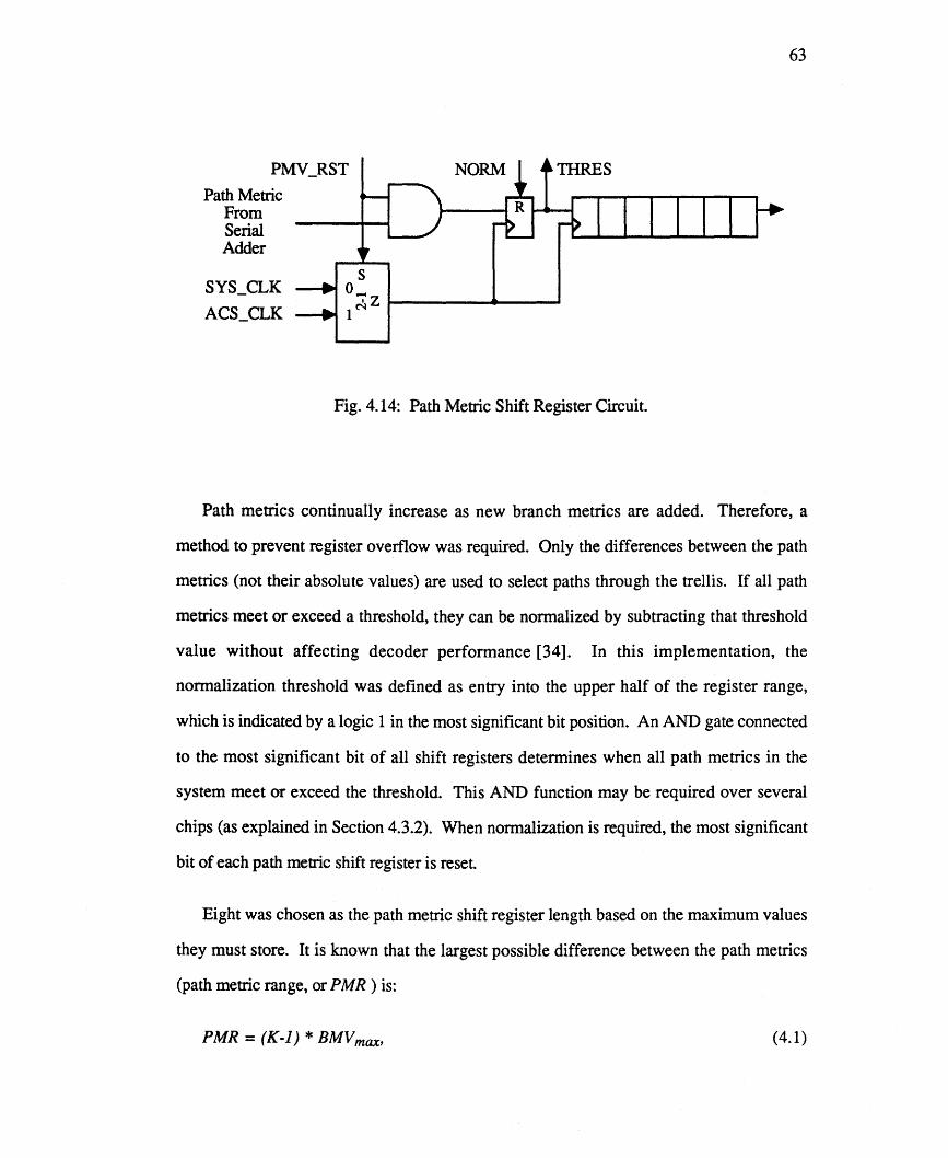
63
PMV_RST
Path Metric From Serial Adder
s SYS_CLK 0_
1~t Z 1--------------'
ACS_CLK
Fig. 4.14: Path Metric Shift Register Circuit.
Path metrics continually increase as new branch metrics are added. Therefore, a
method to prevent register overflow was required. Only the differences between the path
metrics (not their absolute values) are used to select paths through the trellis. If all path
metrics meet or exceed a threshold, they can be normalized by subtracting that threshold
value without affecting decoder performance [34]. In this implementation, the
normalization threshold was defined as entry into the upper half of the register range,
which is indicated by a logic 1 in the most significant bit position. An AND gate connected
to the most significant bit of all shift registers determines when all path metrics in the
system meet or exceed the threshold. This AND function may be required over several
chips (as explained in Section 4.3.2). When normalization is required, the most significant
bit of each path metric shift register is reset.
Eight was chosen as the path metric shift register length based on the maximum values
they must store. It is known that the largest possible difference between the path metries
(path metric range, or PMR ) is:
PMR = (K-l) * BMVmax1 (4.1)
64
where BMVmax is the largest branch metric value in the system [8]. The largest path
metric, PMVL, and the smallest path metric, PMVS, are related as follows:
PMVL = PMVS + PMR. (4.2)
Normalization will not occur as long as PMVS is smaller than the normalization threshold
(NT). Therefore, the maximum value of PMVL is:
PMVL(max) = (NT - 1) + PMR. (4.3)
PMVL is the smaller of two results of an add-compare-select operation. The larger result,
which will be discarded but still must be stored, can exceed PMVL(max) by BMVmax:
ACSmax = PMVL(max)+ BMVmax. (4.4)
With an X-bit path history shift register, the normalization threshold and largest values that
can be stored are:
NT= r-1, (4.5)
and
XACSmax =2 -1. (4.6)
Using equations 4.1 through 4.6 and solving for constraint length K, the following
relationship was derived:
(4.7)
Since the largest bit metric is 6, BMVmax at R=II2 is 12; at R=II3, 18. The maximum
constraint lengths (Kmax) as a function of path metric shift register length are shown in
Table 4.4.

65
Table 4.4: Maximum Constraint Length as a Function of Path Metric Shift Register Length.
Path Metric Upper Constraint Length (K ) Limit Shift Register Length (bits) R= 1/2 R = 1/3
56 1
12
7 5 38 10 79 21 14
After the add-compare-select operation, the rising edge of the control signal TOM
latches the output of the serial comparator. This is necessary to select which path history to
update and which path metric to use during the next add-compare-select calculation. The
serial adder carry bit flip-flops are reset by the signal ACS_RST. The reset is not needed
during regular operation, since (from equation 4.4) ACSmax will never exceed 253. The
ability to reset is required for proPer circuit initialization on startup. The serial comparator
is not reset.
4.2.2 Path history update
At the end of the add-compare-select operation, the change in state of TOM directs the
path histories (as selected by the add-compare-select results) to the node processor output
pins onto the bit-serial recirculation edge. By multiplexing the the path metrics and path
histories onto one bit-serial communication path, the overall amount of wires needed is
reduced.

66
NB_SEL=O r--~..,
~Z
1
Shift 1
S o z ~
Shift 2
S o z ~
Shift 3
S o
z ~
•Oldest Bit
Discarded
Fig. 4.15: Path History Update Algorithm.
Fig. 4.15 illustrates the path history update algorithm. For an X-bit path history shift
register, X-I shifts are required. Initially, the oldest bit is in the rightmost shift register
position. Immediately to the left is the youngest bit. Proceeding left through the shift
register, the age of the path history bits increases, until the second oldest bit is found in the
leftmost position. The output of the path history shift register is connected to a 2-1
multiplexer, called the new bit multiplexer. The output of that multiplexer is connected, via
the bit-serial recirculation edge, to a path history shift register input, which mayor may not
be on the same shift register as the output (it is shown as the same one in the example of

67
Fig. 4.15). On the frrst shift,the signal NB_SEL from the control circuit is low, which
shifts the new bit into the shift register, and discards the oldest bit. NB_SEL goes high,
and the remaining X-2 shifts move the new bit into the youngest bit position, with the
previous youngest bit becoming the second youngest bit. Meanwhile, what was the second
oldest bit becomes the oldest bit, and so on.
The upper node processor updates the path history for a node into which both arriving
branches are upward moving. Thus a new bit of 0 is appended regardless of which path
history is selected. Similarly, the lower node processor always appends a new bit of 1.
Apart from the order of the add-compare-select inputs, the new bit values are the only
difference between the upper and lower node processors of a node processor pair.
As discussed in Chapter 2, a path history length of between 4 and 5 times the constraint
length is desirable. For this design, a path history length of 24 bits was chosen for several
reasons. Circuits with path history shift registers longer than 24 bits did not fit into the
area available. Furthennore, longer path histories reduce the maximum decoding speed,
since more bits must be shifted per decoding step. Finally, longer path histories are not
required in order to verify the operation of the bit-serial architecture. A length of 24 bits
has the added convenience that a total of 31 bits must be shifted per decoding step (eight
path metric bits and 24-1 path history bits). This enables the two node processor clocks
(ACS_CLK and PH_CLK) to be generated using a single five-bit counter in the control
circuit
Since path histories of 24 bits must be accumulated before meaningful data will emerge
from the decoder, the ability to clear the path history shift registers on startup is not
required. Therefore, non-resettable D-type flip-flops were used to construct these
registers. Decoded output data lags the received symbol sequence by 24 bits.

68
4.3 Output Circuit Architecture
The output circuit is responsible for the following tasks: 1) detennining the decoded
output data based on the accumulated path histories, and 2) managing the path metric
normalization signals.
4.3.1 Decoded output data determination
By reconstructing the path taken by the encoder through the trellis, the decoder can
estimate the original data sequence. It is shown in Chapter 2 that practical implementations
of the Viterbi algorithm are restricted to truncated path histories. Even with such a
restriction, several methods to detennine the decoded output data were proposed. These
methods include: 1) minimum metric path history selection, 2) a majority vote among the
oldest bits from all path histories, and 3) arbitrary path history selection.
Selecting the path history with the smallest metric at the end of each decoding cycle and
using its oldest bit as the decoded output is known as maximum likelihood decoding. This
method results in the lowest bit-error-rate for a given path history length [8]. Path history
lengths of 4 to 5 times the constraint length should be used with this technique [7]. It is
not practical for the bit-serial Viterbi Processor architecture, however, because the path
histories and metrics are distributed over multiple chips in cascaded systems, and no circuit
has access to all path metries to determine which is smallest
The second method involves taking a majority vote among the oldest bits of all the path
histories to determine the decoded output bit. This method requires path history lengths of
5 to 6 times the constraint length to achieve bit-error-rates similar to the maximum
likelihood technique [7].
The third method is to arbitrarily select a path history and use its oldest bit as the
decoded output data bit. This method works because the path histories tend to overlap in

69
older positions. Path history lengths of 8 to 10 times the constraint length should be used
for bit-error-rates similar to the maximum likelihood technique [7]. This method is
possible with the bit-serial Viterbi Processor architecture. However, it was rejected
because of the path history length requirements.
Therefore, a majority vote method was chosen for this implementation. The problem of
path histories being distributed over multiple Viterbi Processor chips still remained. Three
methods were proposed for overcoming this problem: 1) an internal majority vote, 2) an
external majority vote, and 3) a hybrid majority vote.
With an internal majority vote, each Viterbi Processor would independently perform a
vote among all the oldest bits in the system. The result from any chip could be used as the
decoded data output bit. This method was rejected because the chips would have to
exchange oldest bit information among themselves, adding to the complexity of the circuit.
Each chip would also require knowledge of the constraint length of the system in which it
was being used. Furthermore, exchanging the oldest bit information could become the
limiting factor in the maximum decoding speed.
The second method of overcoming the distributed path history problem would be to
Perform an external majority vote. The oldest bits of each path history appear on the
recirculation edge after every path history update. Using these outputs, external circuitry
could perform a majority vote. A control signal indicating that the oldest bits are valid
would have to be supplied. This method is simplest (in terms of Viterbi Processor
implementation) because no internal circuitry would be required. However, external
circuitry would be required even for single Viterbi Processor chip decoders.
A hybrid compromise between the internal and external majority vote methods was
selected. Each Viterbi Processor counts the number of logic 1s among its eight oldest bits.
This number is output on three pins, as shown in Table 4.5. An output signal generated by
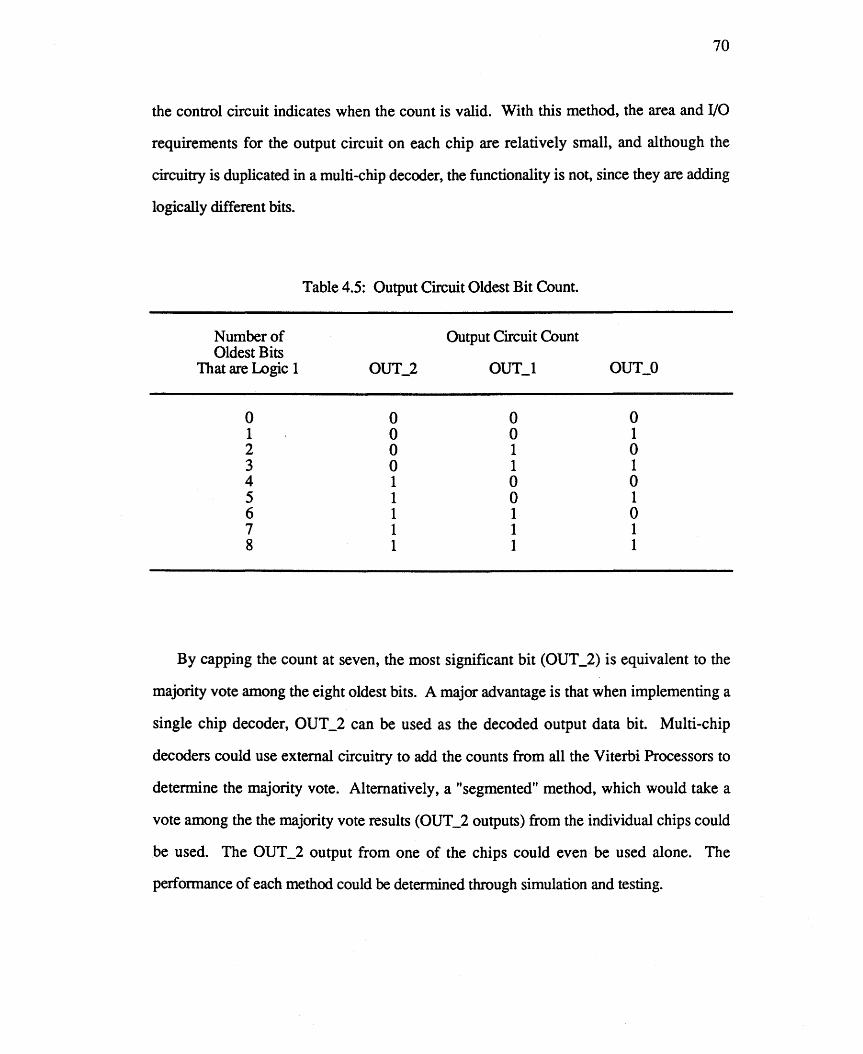
70
the control circuit indicates when the count is valid. With this method, the area and I/O
requirements for the output circuit on each chip are relatively small, and although the
circuitry is duplicated in a multi-ehip decoder, the functionality is not, since they are adding
logically different bits.
Table 4.5: Output Circuit Oldest Bit Count.
Number of Output Circuit Count Oldest Bits
That are Logic 1
o 1
ooo o o 1
2 o o1o
11o
345678
o 1 1 111
o 1111
o 1 1
By capping the count at seven, the most significant bit (OUT_2) is equivalent to the
majority vote among the eight oldest bits. A major advantage is that when implementing a
single chip decoder, OUT_2 can be used as the decoded output data bit. Multi-chip
decoders could use external circuitry to add the counts from all the Viterbi Processors to
determine the majority vote. Alternatively, a "segmented" method, which would take a
vote among the the majority vote results (OUT_2 outputs) from the individual chips could
be used. The OUT_2 output from one of the chips could even be used alone. The
performance of each method could be determined through simulation and testing.

71
The majority vote circuit is shown in Fig. 4.16. Using an 8-1 multiplexer, the bits are
selected, latched, and logically ANDed with a clock to provide count pulses to a three-bit
counter. Since there may be eight oldest bits of logic 1, the ALL_SET output of the three
input NAND gate inhibits further count pulses when the count reaches seven.
Majority Vote Outputs
From Control (OUT_O - OUT_2) Circuit
5-Bit Counter
CO C1 C2
50 51 5201 2 ~
3 ::I Z:E45 -006 7
1------4------0--+1------+----..--1--+ 1------+----+---2-~
+5
Fig. 4.16: Majority Vote Circuit.
The count must be perfonned when the oldest path history bits are valid. As shown in
the timing diagram of Fig. 4.13, the path history shift register contents are stable while the
add-compare-select oPerations are being carried out. Conveniently, the eight pulse signal
ACS_CLK is available during this time. By using the three least significant bits from the
5-bit counter that generates ACS_CLK to select the 8-1 multiplexer input, and ACS_CLK
to latch the multiplexer output and clock the three bit counter, the eight oldest bits can be
added. The node processor control signal NB_SEL changes state after the last ACS_CLK
pulse, and is therefore used to indicate a valid output count via the output pin
72
4.3.2 Normalization circuit
The second part of the output circuit is the nonnalization circuit. This circuit detects
path metric nonnalization conditions and issues nonnalize signals to the node processors.
Detecting nonnalize conditions is a logical "AND" operation, which is easy to segment.
Each Viterbi Processor logically ANDs its most significant path metric bits (THRES_O
THRES_7) and generates a nonnalization request signal, NORM_REQ, which is in turn
logically ANDed with NORM_REQ signals from other Viterbi Processors. In a single chip
decoder, the NORM_REQ output pin would be connected directly to the NORM_GRANT
input pin. In multi-chip decoders, when every chip simultaneously generates a
nonnalization request, NORM_GRANT is asserted and nonnalization proceeds.
The logical AND between Viterbi Processors could be implemented using a
WIRED_AND function. All the NORM_REQ pins would be tied together externally. Any
Viterbi Processor whose metrics do not meet the nonnalization threshold would hold the
signal low. Each chip would monitor the signal, and when all chips require nonnalization,
it would go high and nonnalization would proceed. This method requires no external
circuitry and the internal circuitry is fairly simple. Furthennore, only one I/O pin is
required per Viterbi Processor. However, the WIRED-AND function is difficult to
simulate and is not possible to implement with the standard cell library [36] used for the
rest of the chip. It was decided to use the standard cells only, precluding the WIRED-AND
method. However, it remains a viable option should a second generation Viterbi Processor
be designed.
As shown in Fig. 4.17, each Viterbi Processor logically ANDs its own THRES
signals (one from each node processor) to generate NORM_REQ. The signal ACS_RST
inhibits NORM_REQ from being asserted when the most significant path metric bits are not
valid. NORM_GRANT sets an RS flip-flop, which is reset by the system clock. This

73
insures that the resulting NORM signals, which actually clear the most significant path
metric shift register bits, have wide pulse widths.
ACS_RST
THRES_O
ChipBoundary, , ,
•••,,
,•
External AND
Function
To Sync. Detect
R Circuit ......- ... Q and other
S f4--...IolIlIII-----... Viterbi Processors Q'-'NO-RM-·-_G-RANT--)......
Fig. 4.17: Normalization Circuit.
4.4 Control Circuit Architecture
The control circuit functions are divided into two categories: 1) control and co
ordination of other circuits, and 2) chip interface control. The branch metric, node
processor and output circuits were designed individually based on their required functions.
The control circuit was designed last and its architecture is based on the requirements of the
other circuits. It pipelines the activities of the other circuits to achieve an increased
decoding rate. Fig. 4.18 illustrates the control circuit block diagram. Fig. 4.19 illustrates
the c0t:ttrol circuit timing.

Node Processor Control
t >.~
"E Q.0"::1 "~"3
~~
~~>
C~OCl C2
j ~
l I' ~ ACS_CLKI ~i' 0
~
~
~
,- -- - - - -, 'I I ' , , ,
~--.c READY),, TDM :~ I:
AlP
RST 0- . CYCLE_l-'
r---------------------,, , , , ,, ,, ,
,, , ,, , , ,, J
o -
d l
d ' ~ )-4 U U
'--" Branch Metric __ 9'~I~ ~~l;!l!t~r., , , ,
f-4 CI)
P::I
~~
d >1 ~~
o
~I> ~~
I I To Branch Metric Circuit
Bit Metric Addition Control
To Bit Metric Generator
Circuit
o -Erl
l Erl'
CI) CI)
f-4'-
,- -- ---- ----- ~, , , , , B~_CLK,
'Input Generator ' , , , ,, ,, , , ,-I , RST_O , ,, , , '3-Bit , ,, , , , B~_CLK , , , Counter ' ,, , , , , ,
...... _----" .
Fig. 4.18: Control Circuit Block Diagram.
'_. - _....'
-J ~

75
I
READY --.JRII ---s-m'- ..I'mI,'-_____ a.-.. nL.. rL-
Q.LATCH _1.o.-.__.,I«rt'iR1I~O::·~·_""__.J-,- ....n....__....n
ACS
PMV Shift
Bit Metric Additions
Path History Shift
II~I c;= Path History Shift t
OUT_O-OUT_2XX--------XXX>OOO<X--------X L-
Fig. 4.19: Viterbi Processor Chip Pipelined Operation.
4.4.1 Control and co-ordination
The control tasks are divided into three logically separate functions: 1) received symbol
input and bit metric addition control, 2) branch metric cycle counter, and 3) node processor
and output circuit control. Each bit metric addition is synchronized to the received
sequence input. The rising edge of QLATCH initiates control circuit operation. The next
rising edge of the system clock is detected, then a one clock cycle delay is inserted to allow
the bit metric generation circuit sufficient time to set up its initial outputs. After the one
cycle delay, BMV_CLK is generated. A three-bit counter drives the BIT_SEL inputs on
the bit metric generation circuit, and counts the BMV_CLK pulses. After five pulses, the
input circuitry and the three-bit counter are reset.
Each branch metric calculation requires two or three addition cycles, depending on the
code rate selected. The branch metric cycle control circuit counts the number of bit metric
additions. The signals CYCLE_O and CYCLE_l which control the bit metric routing are

76
generated according to the RATE input (as shown in Fig. 4.8). This circuit also generates
BMV_ZERO. At the end of the last addition cycle, the bit metric cycle counter is reset.
The node processor control circuit monitors BMV_CLK and CYCLE_l to detect the
beginning of the last addition cycle in the branch metric calculation. This indicates that the
branch metrics will be ready for the next add-compare-select operation. A five-bit counter
generates a 31 pulse signal, which is initially routed to the add-compare-select circuitry via
ACS_CLK. After 8 pulses, the remaining 23 pulses are routed to the path history update
circuitry via PH_CLK. At this time TDM is also toggled so that the path histories are
shifted onto the recirculation edge. After the fITSt rising edge of PH_CLK, which indicates
that the new path history bits have been appended, NB_SEL is toggled so that the
remainder of the selected path histories are shifted. At the end of the path history update,
the node processor control circuitry is reset. The node processor control signals also
control the output circuit as described in Section 4.3.
4.4.2 Pipelined operation
To achieve the maximum decoding speed, there should be no delays between the
alternating path metrics and path histories being shifted out on the recirculation edge. Since
branch metrics are required to perform the add-compare-select operations, the branch metric
calculations must be partially completed during the previous path history update (up to the
last bit metric addition cycle as shown in Fig. 4.19) before the add-compare-select can
begin. This pipelining is accomplished by the separate "sub-control circuits" (complete
with separate reset lines) within the control circuit
The timing diagram of Fig. 4.19 illustrates the pipelined operation of the Viterbi
Processor in R =1/3 operation. The shaded portions show the operations belonging to the
same trellis stage. The first two bit metric addition cycles are performed during the
previous path history update. The add-compare-select and path history updates are initiated

77
by the last addition cycle in the branch metric calculation. Therefore, the last bit metric
addition cannot begin before the completion of the previous path history shift. The last bit
metric addition initiates shifting of the branch metrics to the node processors. The
previously selected path metrics are shifted in for the add-eompare-select operation. Then,
the updated path histories are shifted out. The majority vote outputs are not shaded because
the output from the highlighted operations will not emerge for another 24 decoding cycles.
4.4.3 Interface control
The chip interface tasks handled by the control circuit are: 1) encoded symbol input,
2) output vote valid indication, and 3) chip reset control. The received quantized symbols
are written to the Viterbi Processor much like a microprocessor writes data to memory. A
circuit monitors internal signals to determine when the next received quantized symbol can
be written, which is indicated by the READY output pin. Input is allowed if the previous
bit metric addition is complete, unless the next bit metric addition is the last in a branch
metric calculation, in which case the previous path history update must also be complete.
The oldest bits in the path histories are counted by the output circuit during the add
compare-select operation. The resulting output is stable while the path histories are being
shifted. The signal NB_SEL (as shown in Fig. 4.13) is high when the majority vote result
is valid, and so is used to indicate a valid majority vote output via the pin VALID_OUT.
The last interface function handled by the control circuit is the system reset. The three
separate "sub-control" circuits in the control circuit can each be reset individually for
pipelining purposes. Each of these circuit reset signals is logically ORed with the system
reset input pin, SYS__RST, so that the Viterbi Processor can be completely reset on startup.
SYS_RST is also connected directly to the PMV_RST inputs on the node processors,
which clears the path metric shift registers. Therefore, SYS_RST must be asserted for
eight clock cycles to properly initialize the Viterbi Processor chip.
5. VLSI IMPLEMENTATION AND TESTING
Several strategies were considered for implementation of the bit-serial Viterbi Processor
architecture. A bread board method using commercially available discrete components was
proposed. This would verify the architecture, provide performance measurements, and
could identify potential problems. Because this architecture was designed for integrated
circuit implementation, the bread board method would require approximately 150 chips. A
second option considered was a full custom VLSllayout. This would minimize the area
requirements and could increase the maximum expected clock rate. It was felt, however,
that the risk of non-working chips outweighed the potential benefits.
A VLSI implementation using a proven standard cell library and silicon compiler was
chosen. The Northern Telecom 3-micron double metal CMOS process (CMOS3DLM)
offered by the Canadian Microelectronics Corporation (CMC) was chosen for the
implementation [37]. Given the increasing sophistication of the software design tools
available, it was felt that there would be a good chance of obtaining working chips with the
fust prototype. Not only would the architecture be verified, but its suitability for VLSI
implementation would also be demonstrated. This chapter discusses the tools used in the
architecture development, the resulting VLSI implementation, and test results from the
fabricated chips.
78

79
5.1 Development Environment
The tools used to develop the Viterbi Processor architecture are illustrated in Fig. 5.1.
Arrows indicate sequence of use. Circuits are described using a subset of a language called
Very High Speed Integrated Circuit Hardware Description Language (VHDL). This
language has the capability to hierarchically describe a system's structure (architecture) and
its behavior. The subset used in this work describes a system's architecture only. Using a
VHDL compiler [38], the circuit descriptions can be translated into command files for use
by the Queen's University Asynchronous Interactive Logic (QUAIL) Design System [39],
or by the Queen's University Interactive Silicon Compiler (QUISC) [38].
Fig. 5.1: Viterbi Processor Chip Development Environment.

80
QUAil.. is a mixed mode simulator that can simulate at the transistor, gate, or system
level. It uses a Hardware Description Language (HDL) based on VHDL. The VHDL
circuit descriptions are a valid subset of HDL. QUAil.. can be used to verify that the circuit
description is logically correct. Simulation at this early stage reduces the chance of error
and can reduce overall design time requirements. However, as indicated by shading in
Fig. 5.1, QUAil.. was not available during the Viterbi Processor development.
After a QUISC command file has been generated, the program ELECTRIC [40] is run.
ELECTRIC is a general purpose object oriented system for electrical design, and can be
used as a schematic editor and printed circuit board layout tool as well as a VLSI layout
tool. QUISC is called from within ELECTRIC. The user can interactively specify the
number of "rows" for QUISC to use, then pass control to the command file generated by
the VHDL compiler. QUISC uses cells from a user definable standard cell library [36] to
implement the circuit. The silicon compilation consists of two distinct phases. First, the
cells are placed (according to the specified number of rows) resulting in a rectangular
structure. Inter-cell routing is done using routing channels between the rows. By
changing the number of rows, the user has indirect control over the aspect ratio of the
resulting circuit. The second phase in the compilation involves entering the compiled
circuit into ELECTRIC's database. The two phase approach allows QUISC to be modified
for use with layout tools other than ELECTRIC.
After compilation is complete, control returns to ELECTRIC. At this point, the
compiled circuit exists as an entity in ELECTRIC's database and can be edited or stored.
An extraction program can then be called to generate a netlist of the circuit. Using
PRES1M, the netlist can be preprocessed for use with the RNL [41] simulator. PRESIM
uses parameters stored in a user definable configuration fue to calculate the capacitance of
each electrical node and resistance of each transistor channel. PRESIM can also perform
gate reduction which reduces the number of transistors that must be simulated.

81
RNL is a timing logic simulator for digital MOS circuits. It estimates transition times
based on the resistance and capacitance values calculated by PRESIM. It is also possible to
perform device level simulations on the extracted circuits using programs such as
SPICE [41]. Device level simulation involves accurate voltage and current calculations
with sub-nanosecond resolution at each node. Serbin [39] states that a properly calibrated
device level simulator should predict, within a few percent, actual current flow through a
transistor. PRESIM and RNL, when accurately calibrated, should predict timing estimates
within 20% of SPICE results. For the development of the Viterbi Processor, Serbin and
Kostiuk's PRESIM configuration file [42] was used. It was generated by implementing
the standard cells, measuring their switching times, and adjusting the PRESIM parameters
until the RNL results matched the measured values.
RNL obtains test vectors from an input command file, and simulation results are piped
to an output file. The program MTPV [43] provides a logic analyzer style plot of the RNL
results. The operation of simple to moderately complex circuits can be verified using
MTPV output. However, it was found that when a complete Viterbi Processor was being
simulated with RNL, the resulting timing diagrams were not sufficient to verify circuit
OPeration. A logic level Viterbi algorithm simulator (VSIM, described in ApPendix B) was
written to calculate the expected internal variable values (branch metrics, path metrics and
histories, etc.). By comparing the RNL results to the VSIM results, correct circuit
oPeration could be verified.
5.2 Viterbi Processor VLSI Layout
The four circuits that comprise the Viterbi Processor were developed independent!y.
These circuits are 1) the branch metric circuit, 2) the node processor circuit, 3) the output
circuit, and 4) the control circuit. Each was simulated and refmed until the desired behavior
was obtained. They were then combined into one large VHDL file which included the
82
"external" connections from node processor outputs to inputs needed to model a trellis
diagram. This task was trivial due to VHDL's hierarchical nature. The entire Viterbi
Processor was compiled using QUISC and simulated using RNL and VSIM. At this stage,
each QUISC compilation required approximately 1500 seconds of CPU time (running on a
microVAX workstation) and each RNL simulation required approximately eight hours of
CPU time. Several design errors in the four circuits were detected and corrected using this
procedure. The resulting VHDL file is listed in Appendix A.
The "external" connections were removed, and the single VHDL file was again
compiled. The largest padframe (size "A") offered by the CMC is 4510 by 4510 microns.
Approximately 300 microns are required along each edge for the I/O pads and associated
circuitry, leaving a 3910 by 3910 micron area (15.3 x 1()6 microns2) for the design. When
compiled on 26 rows, the complete Viterbi Processor required 4720 by 3931 microns (18.5
x 1()6 microns2), exceeding available area by 17%. To overcome the area limitations, the
four individual circuits were compiled separately and placed manually. Each circuit was
compiled with several different aspect ratios. Combinations of circuits blocks were tried
until all circuits were successfully placed into the area available. Then, all inter·circuit
wiring was done manually. The QUISC2 compiler [44], which is currently under
development, will automate the floorplanning, block placement and inter·block routing
tasks.
When the manual layout was complete (including I/O pads), external connections were
placed between the node processor output and input pins. Extensive RNL and VSIM
simulations were again carried out and a number of wiring errors were found and
corrected. Once simulation indicated correct operation, the external connections were
removed. After extensive design rule checking, the completed design was sent in CaItech
Intermediate Format (CIF) to the CMC for fabrication. The resulting integrated circuit was

83
named University of Saskatchewan Viterbi Processor version B (SKVPB). The floorplan
of SKVPB is shown in Fig. 5.2.
Control Circuit
.::s & 8
Fig. 5.2: Plot of SKVPB.

84
5.3 VLSI Chip Test Results
Before SKVPB was fabricated, a test chip (SKVPA) containing a branch metric circuit
and one node processor pair was implemented. All five SKVPA chips received from the
CMC oPerated as expected, at clock rates up to 25 Mhz. Since 31 shifts must be performed
per decoding step, this clock rate indicates a potential decoding speed of 780 kbps. After
the branch metric circuit and node processor circuits were verified by SKVPA, the chip
SKVPB was submitted for fabrication. A total of 15 SKVPB chips were received from the
CMC, ten from lot "A", five from lot "B" (the different lots being different fabrication
runs). One chip from lot "A", and two chips from lot "B" operated as expected. The
failure modes of the non-working chips varied from completely dead to an estimated 95%
functionality. The maximum clock rate of the three working chips ranges from 8.5 Mhz to
9.2 Mhz, which translates to decoding speeds of 265 kbps to 287 kbps. This is
considerably slower than the potential speeds indicated by the SKVPA test results. The
difference could be due to inter-circuit timing requirements and layout dependant clock
skew not tested by SKVPA. Further RNL simulation might identify the limiting speed
factor in SKVPB.
5.3.1 Detailed SKVPB testing
The SKVPB test setup is shown in Fig. 5.3. A photograph of the setup is shown in
Fig. 5.4. The H.P. 8180A Data Generator was used to supply the test vectors, and the
H.P. 8182A Data Analyzer was used to observe the results. Since all path histories and
path metrics are shifted out with every decoding cycle, the chip is highly testable in its
present form. Because two chips are required to implement R=l13 decoders, individual
chips were tested in R=112 mode only. External connections were made to model a K=4
R=112 trellis with gj=15 and g2=17. A single stage of the trellis diagram is shown in
Fig. 5.5.

85
Recall that each upward moving branch represents a source data bit of logic 0, and each
downward moving branch represents a source data bit of logic 1. The decoder estimates
the source data sequence by determining the most likely path the encoder has taken through
the trellis. Starting and ending at node 0, a sequence of 16 branches was chosen such that
every possible trellis branch was taken. From these branches, the encoded symbol
sequence shown in Table 5.1 was determined. The chips were tested by repeatedly
shifting in the 32 encoded symbols. With the repeating 32 symbol sequence, every shift
register, serial adder and serial comparator on the chip is exercised. The output circuit
(both majority vote and normalize portions) are completely tested. Since all branches are
taken, all multiplexers are fully tested. However, the circuitry which allows R=1/3
operation is not fully exercised, and not all possible branch metrics are calculated. With
this test vector, it is estimated that more that 99% of the chip is tested.
--.. INV Bl '-I BMV SET fOIllIt-GND --~ INV-BO OUT 2 .....
GND - -~ INV-Al OUT-l ... --~ INV-AO OUT-O ..... .... ~ GND NORM_REQ ....
+5 o-~ RATE NORM_GRANT I
Q2 VDD ~k)+5..... Ql 17 ..... QO ~ IS ..... ... &kATCH Q.. 13 .... > II ....
.... RESET ~ 16 ..... ~ .... ACS CLK en 14 ....,
READY I2 ..... .... VALID_OUT 10 fIlIII I-- .. VDD 07 ...
....... GND 06 ..... -4II1II 00 05 ...
.... 01 04 .... ..... 02 03 ...
Fig. 5.3: SKVPB Pinout and Test Setup.

86
Fig. 5.4: Photograph of SKVPB Test Setup.
Table 5.1: 16-Bit Source Data Sequence and Associated Encoded Symbol Sequence.
Source Data Trellis Encoded Symbol Bit Branch Sequence
0 0-0 00 1 0-4 11 1 4-6 00 0 6-3 10 1 3-5 01 1 5-6 11 1 6-7 01 1 7-7 10 0 7-3 01 0 3 - 1 10 1 1-4 00 0 4-2 11 1 2-5 10 0 5-2 00 0 2-1 01 0 1 - 0 11

87
Node
,000 11
1
2
3
4
5
6
7
Fig. 5.5: Single Stage of K=4 R=1/2, gj=15, g2=17 Trellis Diagram.
The H.P. 8182A output is shown in Fig. 5.6. As can be seen, the repeating decoded
data output matches the source data bit sequence shown in Table 5.1. As expected, when
there are no errors in the encoded symbol input, the decoder's output votes are all
unanimous. In the "close up" of Fig. 5.7, two decoding cycles are shown. For the
second decoded bit, the outputs OUT_O ~ OUT_2 can be seen counting to 7. The signal
VALID_OUT goes high after the count is complete. One of the node processor outputs is
shown, from which the emerging path metrics and histories can be seen.
When errors were introduced into the encoded symbol sequence, the path metrics began
to grow, causing normalizations to occur. In Fig. 5.8, a normalization signal
(NORM_REQ - NORM_GRANT) can be seen at the end of a decoding cycle. Fig. 5.9
illustrates the effects of loss of branch synchronization. Since the symbols appear random,
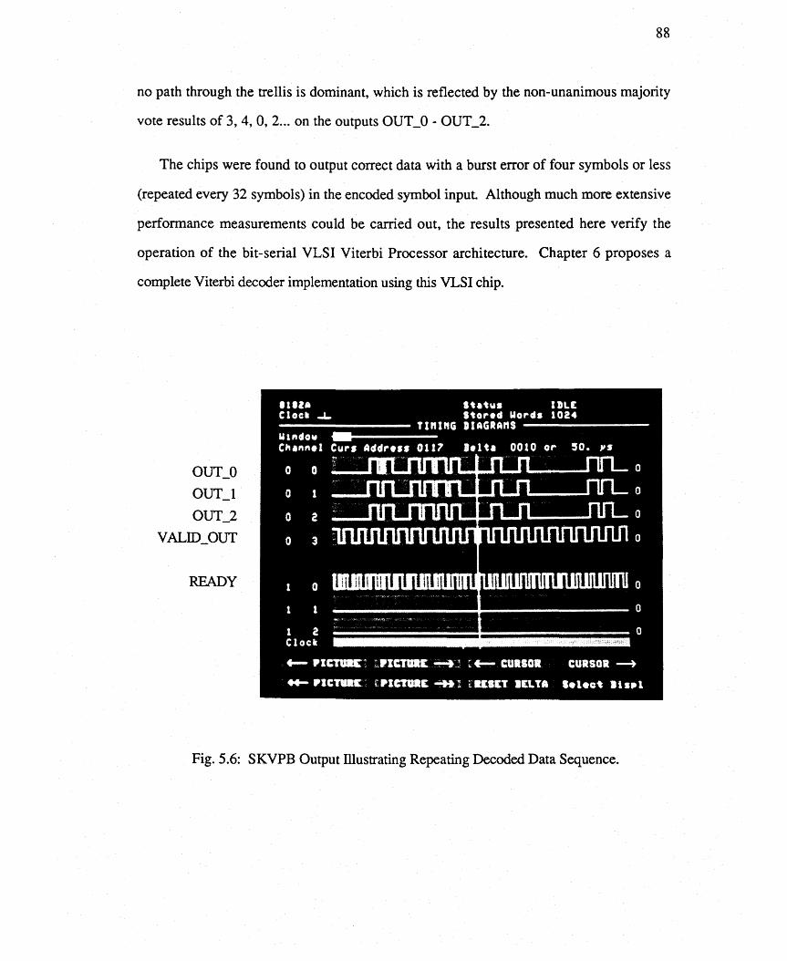
88
no path through the trellis is dominant, which is reflected by the non-unanimous majority
vote results of 3, 4, 0, 2... on the outputs OUT_O - OUT_2.
The chips were found to output correct data with a burst error of four symbols or less
(repeated every 32 symbols) in the encoded symbol input Although much more extensive
performance measurements could be carried out, the results presented here verify the
operation of the bit-serial VLSI Viterbi Processor architecture. Chapter 6 proposes a
complete Viterbi decoder implementation using this VLSI chip.
OUT_O
OUT_l
OUT_2
VALID_OUT
READY
Fig. 5.6: SKVPB Output illustrating Repeating Decoded Data Sequence.

89
OUT_O
OUT_l
OUT_2
VALID_OUT
READY
NODE PROCESSOR
OUTPUT
Fig. 5.7: SKVPB Output illustrating Majority Vote Outputs and One Node Processor Output.
OUT_O
OUT_l
OUT_2
VALID_OUT
Fig. 5.8: SKVPB Output illustrating NORM_REQ Signal.
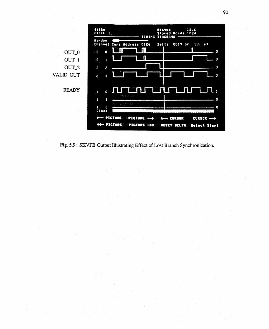
90
OUT_O
OUT_l
OUT_2
VALID_OUT
READY
Fig. 5.9: SKVPB Output Illustrating Effect of Lost Branch Synchronization.
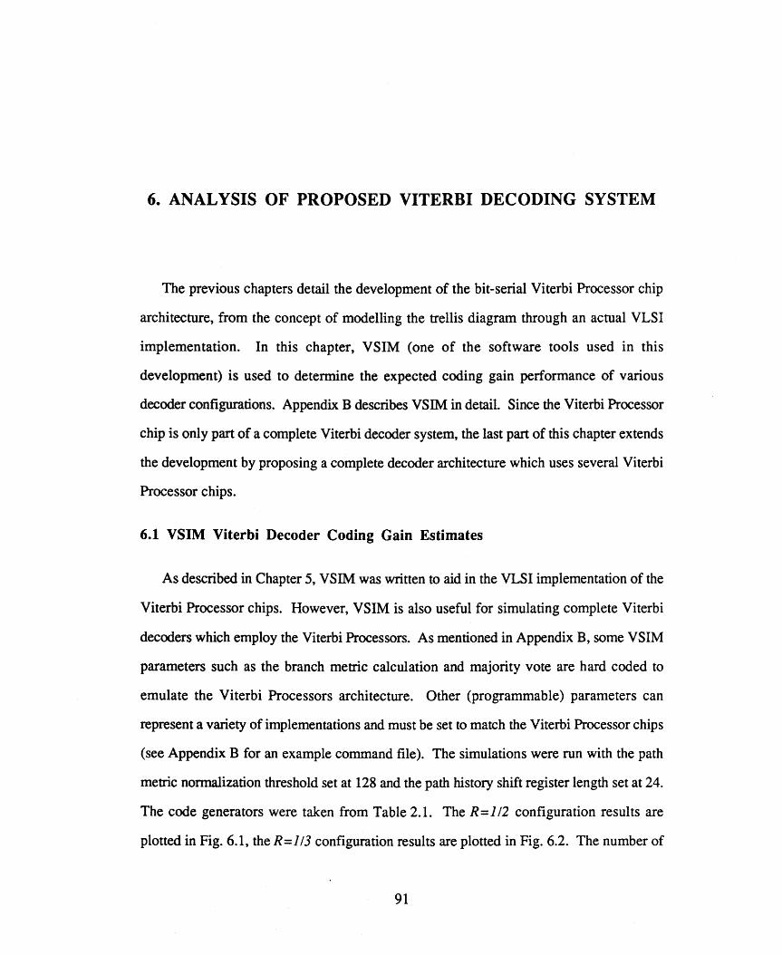
6. ANALYSIS OF PROPOSED VITERBI DECODING SYSTEM
The previous chapters detail the development of the bit-serial Viterbi Processor chip
architecture, from the concept of modelling the trellis diagram through an actual VLSI
implementation. In this chapter, VSIM (one of the software tools used in this
development) is used to determine the expected coding gain performance of various
decoder configurations. Appendix B describes VSIM in detail. Since the Viterbi Processor
chip is only part of a complete Viterbi decoder system, the last part of this chapter extends
the development by proposing a complete decoder architecture which uses several Viterbi
Processor chips.
6.1 VSIM Viterbi Decoder Coding Gain Estimates
As described in Chapter 5, VSIM was written to aid in the VLSI implementation of the
Viterbi Processor chips. However, VSIM is also useful for simulating complete Viterbi
decoders which employ the Viterbi Processors. As mentioned in Appendix B, some VSIM
parameters such as the branch metric calculation and majority vote are hard coded to
emulate the Viterbi Processors architecture. Other (programmable) parameters can
represent a variety of implementations and must be set to match the Viterbi Processor chips
(see Appendix B for an example command file). The simulations were run with the path
metric normalization threshold set at 128 and the path history shift register length set at 24.
The code generators were taken from Table 2.1. The R =1/2 configuration results are
plotted in Fig. 6.1, the R=1/3 configuration results are plotted in Fig. 6.2. The number of
91
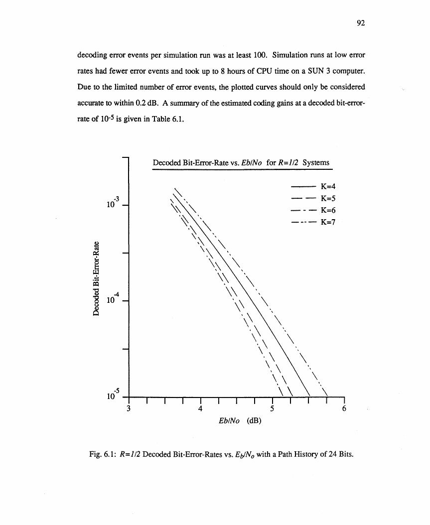
92
decoding error events per simulation run was at least 100. Simulation runs at low error
rates had fewer error events and took up to 8 hours of CPU time on a SUN 3 computer.
Due to the limited number of error events, the plotted curves should only be considered
accurate to within 0.2 dB. A summary of the estimated coding gains at a decoded bit-error
rate of 10-5 is given in Table 6.1.
Decoded Bit-Error-Rate vs. Eb/No for R=1/2 Systems
-3 10
£ ~= ~g ~
I...• .-4
~
"E -4] 10
Co)
Q
-5 10
3
Eb/No (dB)
Fig. 6.1: R=1/2 Decoded Bit-Error-Rates vs. EiJNo with a Path History of 24 Bits.
K=4
---- K=5
-- K=6 -.....--- K=7
, ,
, ,
,
\ \
\ . \
4 5 6

93
Decoded Bit-Error-Rate vs. EblNo for R=113 Systems
-3 10
--K=5
- - K=6
-~- - K=7
2 3 4 5
EblNo (dB)
Fig. 6.2: R=113 Decoded Bit-Error-Rates vs. EJJNo with a Path History of 24 Bits.
Table 6.1: Coding Gain Estimates (With 24-bit Path History).
Coding Gain Estimates (dB) at Decoded BER of 10-5
Constraint Length R=112 R=113
4 4.0 5 4.3 4.8 6 4.4 5.2 7 3.8 5.0
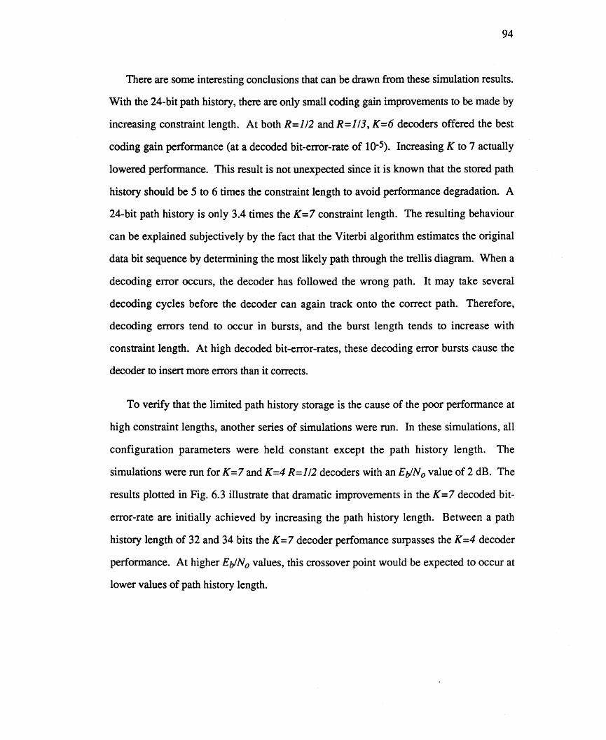
94
There are some interesting conclusions that can be drawn from these simulation results.
With the 24-bit path history, there are only small coding gain improvements to be made by
increasing constraint length. At both R=1/2 andR=1/3, K=6 decoders offered the best
coding gain performance (at a decoded bit-error-rate of 10-5). Increasing K to 7 actually
lowered perfonnance. This result is not unexpected since it is known that the stored path
history should be 5 to 6 times the constraint length to avoid performance degradation. A
24-bit path history is only 3.4 times the K=7 constraint length. The resulting behaviour
can be explained subjectively by the fact that the Viterbi algorithm estimates the original
data bit sequence by detennining the most likely path through the trellis diagram. When a
decoding error occurs, the decoder has followed the wrong path. It may take several
decoding cycles before the decoder can again track onto the correct path. Therefore,
decoding errors tend to occur in bursts, and the burst length tends to increase with
constraint length. At high decoded bit-error-rates, these decoding error bursts cause the
decoder to insert more errors than it corrects.
To verify that the limited path history storage is the cause of the poor perfonnance at
high constraint lengths, another series of simulations were run. In these simulations, all
configuration parameters were held constant except the path history length. The
simulations were run for K=7 and K=4 R=1/2 decoders with an ElJNo value of 2 dB. The
results plotted in Fig. 6.3 illustrate that dramatic improvements in the K=7 decoded bit
error-rate are initially achieved by increasing the path history length. Between a path
history length of 32 and 34 bits the K=7 decoder perfomance surpasses the K=4 decoder
performance. At higher E1JNo values, this crossover point would be expected to occur at
lower values of path history length.
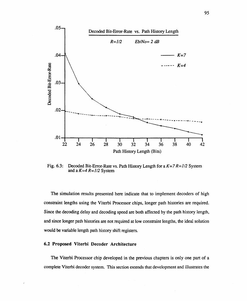
95
.05 Decoded Bit-Error-Rate vs. Path History Length
R=1/2 Eb/No= 2 dB
K=7
.01-1---...... ........ __--_-_--...--......-.....----.-----.
.04
~~~
§ ~ .03~.... ~
13 "8 (,)
8 .02 -.'
22 24 26 28 30 32 34 36 38 40 42
Path History Length (Bits)
Fig. 6.3: Decoded Bit-Error-Rate vs. Path History Length for a K=7 R=l/2 Systemand aK=4 R=1/2 System
The simulation results presented here indicate that to implement decoders of high
constraint lengths using the Viterbi Processor chips, longer path histories are required.
Since the decoding delay and decoding speed are both affected by the path history length,
and since longer path histories are not required at low constraint lengths, the ideal solution
would be variable length path history shift registers.
6.2 Proposed Viterbi Decoder ArChitecture
The Viterbi Processor chip developed in the previous chapters is only one part of a
complete Viterbi decoder system. This section extends that development and illustrates the

96
use of the Viterbi Processor by proposing a complete decoder design. Although decoder
designs utilizing this chip can vary widely, certain functions must be added or completed
externally. These functions include: 1) normalization condition detect (in cascaded
systems), 2) majority vote (in cascaded systems), 3) demodulation, and
4) synchronization.
Given today's technology, microprocessor controlled decoders warrant serious
consideration. The microprocessor could perform statistical analysis on the incoming and
decoded data. Data quality could be estimated by monitoring normalization rates and
majority vote results. The microprocessor may even be able to perform some of the
required tasks, such as synchronization, normalize condition detect, and the majority vote.
However, the Viterbi Processor chip can be used in very basic decoder designs and is not
limited to decoder systems containing microprocessors.
The frrst step in designing a complete decoder is to determine what code rate and
constraint length are needed to meet the coding gain requirements. This can be done using
the estimated coding gains presented in Section 6.1. For this discussion, a required
coding gain of 4.3 dB at a decoded bit-error-rate of 10-5 has been assumed. From
Fig. 6.1, a K=5 R=1/2 decoder will meet this requirement. A K=5 decoder requires two
Viterbi Processor chips. The next step is to determine the trellis diagram characteristics
upon which the external wiring is based. This can be done using VSIM, with the
appropriate parameters specified, and the command "display trellis" included in the
command file. The VSIM output for the chosen configuration is shown in Fig. 6.4.
Recall from Chapter 2 that there are two branches leaving every node in the trellis. One
corresponds to a new source data bit of logic 0 being shifted into the encoder, the other
corresponds to a new bit of logic 1. For each of the sixteen nodes in one stage of the
trellis, the two nodes in the next stage and the encoded symbol sequence associated with
the two branches are shown.

97
VITERBI PROCESSOR SIMULATOR VERSION V2.0 PARAMETER FILE: prm.O DISPLAY TRELLIS DISPLAY STATISTICS PATH HISTORY: 24 CONSTRAINT LENGTH: 5 NORMALIZE: 128 RATE: 1/2 G1 (CODE GENERATOR 1 OCTAL) : 23 G2 (CODE GENERATOR 2 OCTAL) : 35 Eb/No: 4.0 STATISTICS: 10000 RESYNCHRONIZATION THRESHOLD: 0 QUIT AFTER RECEIVED SYMBOLS: 0
START NODE
NEW BIT=O DEST. ENC. NODE SEQ.
NEW BIT=l DEST. ENC. NODE SEQ. PAIR INV XX
0: 1 :
0 0
00 11
8 8
11 00
AO (CHIP 1) 0
2 : 3 :
1 1
10 01
9 9
01 10
B1 (CHIP 1) 0
4 : 5 :
2 2
01 10
10 10
10 01
BO (CHIP 1) 0
6: 7 :
3 3
11 00
11 11
00 11
A1 (CHIP 1) 0
8 : 9 :
4 4
01 10
12 12
10 01
BO (CHIP 2) 0
10: 11:
5 5
11 00
13 13
00 11
A1 (CHIP 2) 0
12: 13:
6 6
00 11
14 14
11 00
AO (CHIP 2) 0
14: 15:
7 7
10 01
15 15
01 10
B1 (CHIP 2) 0
Fig. 6.4: VSIM Output for a K=5 R=1/2 Code with One Possible Node Processor Pair Allotment Shown.

98
Appropriate 'node processors pairs can be selected by matching the encoded sequences
shown in Table 4.3 to those shown above (the encoded sequences shown in Table 4.3 are
for the upper branches only). Each node processor pair implements a butterfly subsection
of the trellis by performing operations for nodes which differ by their most significant bit.
Their outputs go to the nodes for which they perform the operation, as shown in Fig. 3.3.
Therefore, they can be related to the corresponding physically adjacent nodes in the
previous stage of the trellis for wiring purposes. One possible allotment of node processor
pairs is shown in Fig. 6.4 (this allotment is not output by VSIM). From this allotment, the
external wiring of the Viterbi Processors shown in Fig. 6.5 can be determined. The
sixteen-bit recirculation edge (RO-R15) feeds the node processor outputs from each Viterbi
Processor chip back to the inputs. For example, the output of node processor AO_O goes
to node 0 and the output of node processor AO_l goes to node 8, which is indicated by the
wires RO and Rl. In this case, the!NV input for each node processor pair is tied low. The
RATE input on each chip is tied high, which indicates R=lt2 operation. The BMV_SET
inputs, which are not considered during R=lt2 operation are also tied high.
6.2.1 Majority vote and normalization
The 3-bit majority vote output (OUT_O - OUT_2) from each Viterbi Processor chip
provides a count of the number of oldest path history bits that are a logic 1 (as described in
Section 4.3.1). In a cascaded system, there are several ways to determine the decoded
data bit. In this proposed design, the complete counts are added using a 4-bit full adder, as
shown in Fig. 6.5. Since the counts are each capped at seven, the the most significant bit
of each 4-bit adder input is tied low and the largest result possible is fourteen. Therefore,
the most significant output bit of the 4-bit adder can be used as the majority logic decoded
output bit.

99
Clock Reset
Vdl NORM R Vdl NORM:G BMY SET RATE
Q.LATCHGND GND INV_AO ~INV_AI ~
INV BO tI]
INV:BIVALID our
CLK
RESET
10 AO11 I 12 Al 13 I 14 BO 15 I 16 Bl 17 IRecirculation Edge
/
Vdl NORM_RVdI BMY SET NORM G RATE
Q.LATCHGND GND
READY .......
QO l:8l'8! Q2~
" OUT 0
-'rnOur-I Our:2 " 01
'02
1m I~ RO
I~I ~
Rl R2
I~ R R3 R4
06 I ~
R5107 R6 R7
/16 ~
" READY ~
~~QO
8! ~Q2~rn
01 ~r--,t 02~,
our_o our 1 Our:2
I ~R8
1m R9 RIO
I~ I ~ Rll R12
04 f ~ R13105 RI4
l
...INV_AO ~ V<iI S4INV Al ~ S3tI]
A3 S2 ~ Dec~ed~=~? VALID_Our A2 SI r7' Data
00Al OutCLK B3 8 B2 "I:t
RESET BI CO r,t Rli ~ 10 AO -B4
A4 cfrit I
11 I I I~~ 12 AlRl ~ 13 I
-~ V14 BO~~ 15 I
~ R15R15 ~ 16 Bl 17 I I~
+5
t--I-t--
"'
-~
I-
~
I-~
--.r
ROFR6~R8~
R14 ~R12 ~RIO ~
~v-
'"'- +5
---0....
-~I-I-
~
I-
-=.-=
R13
~r
- ~~
< ...
~~~
i ... 5-
E= ~<t>~
0, ~~~~EZ3~
~ ~>-. tI]
--1\ tLJ
Valid Out
.....+5
Fig. 6.5: Example K=5 R=1/2, gj=23, g2=35 Viterbi Decoder System.

100
The path metric NORM_REQ outputs from each Viterbi Processor indicate that all path
metrics on that chip exceed the normalization threshold (as discussed in Section 4.3.2).
Since all path metrics in the decoder must exceed the threshold before normalization can
proceed, the two normalization request signals are logically ANDed, and the result is
connected to the NORM_GRANT input on each Viterbi Processor chip.
6.2.2 Demodulation and synchronization
The demodulator interfaces to the Viterbi Processor chips as shown in Fig. 6.5. It
converts the analog waveforms received from the transmission channel into estimates of
transmitted symbols and can therefore be thought of as an analog filter followed by a
quantizer [7]. The three most significant quantizer output bits are connected to the Viterbi
Processor received symbol inputs (QO - Q2). The demodulator must also supply a rising
edge on the Q_LATCH input when the symbol inputs are stable. The READY output of
one of the processors is monitored to ensure they are able to accept data. Hard decision
(two level quantization) and four level soft decision can also be supported by tieing the
appropriate inputs together.
The demodulator must also perform two types of input synchronization. Branch
synchronization groups the correct N received symbols together for each decoding step.
Phase synchronization resolves polarity reversal which can occur when PSK modulation is
used. The actual synchronization strategy used depends on the modulation scheme and is
beyond the scope of this thesis. For R=l IN operation, no more that N attempts are
required to synchronize [2].
6.2.3 Lost synchronization detection
In many applications the information destination may be responsible for detecting lost
synchronization. When an excessive error rate in the decoded data is identified, a

101
resynchronization signal is issued to the demodulator. However, the Viterbi decoder can
be made self synchronizing. When synchronization is lost, the received sequence appears
as random symbols. No path through the trellis is dominant, which is reflected by path
metrics which increase rapidly and path histories which do not overlap. Non-overlapping
paths can be detected by monitoring the majority vote results, which tend to be non
unanimous. Rapidly increasing path metrics can be detected by monitoring the number of
decoded bits between path metric normalizations.
Either method is possible to implement with the Viterbi Processor based decoder. For
this proposal, a technique using the path metric normalization rate was investigated. Using
VSIM, the average normalization interval was determined for a K=5 R=112 decoder with
the normalization threshold set to 128. Simulations were run under a range of noise
conditions. During each simulation run, the average normalization interval under
synchronized conditions was recorded. Then, loss of branch synchronization was forced,
and the new average normalization interval was recorded. The results are plotted in
Fig. 6.6. Under synchronized conditions, the normalization interval decreases as the noise
increases, as expected. The results of Fig. 6.6 demonstrate that it is possible regardless of
noise conditions for the Viterbi decoder to differentiate between noise and loss of
synchronization based on the average normalization interval. It is also possible for the
decoder to estimate the noise conditions on the channel.
It is interesting to note that under lost synchronization conditions the normalization
interval increases as the noise increases. This can be explained by the fact that the symbol
sequence appears as a random symbol stream. As the noise increases, the symbols become
more attenuated, resulting in branch metrics of smaller magnitude (when soft decision is
used). Therefore, the path metrics grow more slowly resulting in the decreased
normalization rate.

- -------
102
- -- - -- --
4 Nonnalization Interval vs. Eb/No
K=5, R=1/2
---In Synchronization
-LostSynchronzation
O-+---r-----,~- __--......-_--_r_-~.__-_.,...--...__-....,-1 o 1 2 3
Eb/No (dB)
Fig. 6.6: Average Normalization Interval vs. ElJNo for a K=5 R=1/2 Decoder System.
The normalization intervals plotted in Fig. 6.6 are average values. The actual values
appear to be normally distributed about the mean, as indicated by the VSIM intervals
plotted in Fig. 6.7. If the decoder monitors each individual normalization interval, there is
a certain probability (which can be calculated) that the decoder will fail to recognize a lost
synchronization condition. This is acceptable, because it will resynchronize on a
subsequent normalization interval. As the channel noise increases, the probability of failing
to recognize a lost synchronization condition increases. This translates into a longer
average time requirement to resynchronize. There is also a certain probability that the
decoder will resynchronize when it should not, resulting in corrupted data. As the channel
noise increases, the probability of false resynchronization also increases, a condition which
the designer must try to avoid.
4

- - -
103
Nonnalization Interval Distribution
100 K-S , R-l/2, Eb/No-O dB With Branch Synchronization
80
60 40
20 o I
I 190 200 210 220 230 240 250 260170 180
Nonnalization Interval (Bits)
Fig. 6.7: Normalization Interval Distribution for aK=S R=1/2 System, with EIfN0=0 dB (In Synchronization).
Monitoring the nonnalization interval is a simple process with the Viterbi Processor
chips. An external counter can be used to count decoded data bits. If normalization occurs
before the counter has reached a threshold value, a resynchronization signal is issued to the
demodulator. The counter is reset every time normalization occurs. There is a classic
trade-off involving the design of the lost synchronization detection circuit. By monitoring
multiple normalization intervals over a period of time, the probability of false
resynchronization can be reduced at the expense of increased time required to detect actual
loss of synchronization This is easy to implement using the method described above. The
decoded bit counter threshold would be raised, and only every second or third (or whatever
span is needed) normalization signal is considered.

104
The conceptual development of the bit-serial Viterbi Processor is now complete. This
chapter illustrates that a complete decoder can be based on the Viterbi Processor chips. Not
only can the designer customize the system in terms of coding gain requirements, but also
in terms of false resynchronization probabilities and average resynchronization time
requirements under expected operating conditions. The Viterbi Processor chips can be
used in many applications, from simple decoders which require minimal support circuitry
to powerful, sophisticated decoders which may use microprocessors and perform many
added functions.

7. CONCLUSIONS
7.1 Summary of Viterbi Processor Features
The VLSI Viterbi Processor presented in this thesis implements the Viterbi algorithm (a
method of decoding convolutional codes) using approximated metric values based on the
maximum likelihood metric values. From the received symbol sequence, the decoder
estimates the most likely path taken by the encoder through the trellis (a diagram which is a
graphical representation of encoder operation). This leads to an accurate estimate of the
original source data sequence.
The architecture presented here is fully bit-serial. All computations and
communications are carried out one bit at a time. The architecture can be thought of as a
"model" of the trellis diagram. Each branch in the trellis is implemented with a bit-serial
communication path· (a single wire). The processing requirements of each trellis node are
carried out by bit-serial node processor circuits. Because of their small size, node
processors are dedicated to each node (at one stage) of the trellis. This leads to the term
"bit-serial node-parallel architecture". Because of the regular geometry of the trellis
diagram, the trellis branches were fed back from the node processor outputs to the node
processor inputs, which allows the Viterbi Processor to act as a "sliding window".
Implementing those bit-serial connections externally further reduced on-chip routing
requirements and allows identical Viterbi Processor chips to be cascaded to model larger
trellis diagrams and implement more powerful decoders. By pairing the node processors,
105

106
the number of wires required for the external connections was reduced by 1/2, and the
number of I/O pins required was reduced by 113.
Due to area considerations, the Viterbi Processor chips were implemented with eight
node processor circuits (4 pairs) for a constraint length of K=4 per chip. Eight-bit path
metrics and 24-bit path histories are maintained. The branch metric circuit accepts 2, 4, or
8 level soft decision by the demodulator and calculates the branch metrics required by the
node processors in a bit-serial format. The output circuit performs a majority vote among
the oldest bits of the stored path histories. The VLSI layout was done using the QUISC
silicon compiler and ELECTRIC layout tool. The chip was fabricated through services
provided by the Canadian Microelectronics Corporation. It has 9860 transistors on a 4510
by 4510 micron die, and is packaged in a 40 pin DIP.
Three offlfteen chips fabricated were found to operate correctly. Although this yield is
somewhat low, these chips verify the bit-serial architecture. The maximum clock rates of
the operational chips ranged from 8.5 Mhz to 9.2 Mhz, which translates to decoding
speeds of 265 kbps to 287 kbps. Earlier test chips ran at 25 Mhz, indicating a potential
decoding speed of 780 kbps. Simulations indicate that coding gain improvements degrade
as constraint length is increased, due to the short path history storage. At both R=l12 and
R =113, K=7 decoders performed worse than K=6 decoders. Coding gains range from
4.0 dB (single chip K=4 R=112 decoder) to 5.2 dB (four chip K=6 R=113 decoder).
These results indicate the bit-serial Viterbi Processor chips would be suitable for low cost,
low to medium data rate decoder applications.
7.2 Suggestions for Future Study
Although the bit-serial Viterbi Processor architecture functions as expected, there are
many areas in which further study could be undertaken. Some of these areas are briefly
mentioned in this section.

107
The ability to cascade identical chips to implement more powerful decoders is a feature
unique to this design. To fully take advantage of this feature, simulations indicate that
longer path histories are required. However, longer path histories reduce the maximum
decoding speed. Variable length path history shift registers would allow the coding
gain - decoding speed tradeoff to be tailored to each individual application. Another
feature which could be useful would be the ability to connect the node processor outputs to
the inputs internally. With single chip decoders, external wiring would be reduced. An
input pin could be used to disable this feature which would allow for cascaded OPeration.
The difference between the maximum clock rates of SKVPB and the test chip SKVPA
could be investigated further. Since both the node processor and branch metric circuits
were shown to function correctly at 25 Mhz, it should be possible to operate at clock rates
greater than the 9.2 Mhz achieved. Timing peculiarities between the circuits, and skew
due to the layout are two potential causes of this low clock rate.
There are 340 shift register cells in SKVPB (20 in the branch metric circuit, 40 in each
node processor circuit). They are all implemented using the relatively large and slow static
shift register cells from the standard cell library. A full custom layout using dynamic cells
wherever possible could reduce the area requirements and increase the maximum expected
clock rate. With a 1.5-micron technology, it should be possible to implement Viterbi
Processors of K=6 per chip. There may even be room enough for some functions such as
demodulation and resynchronization which are currently implemented externally. This
would further simplify overall decoder design.
Although the chip is testable in its present form, with added room there are many
changes that could be made to enhance the thoroughness and ease of testing. Some of
these changes include the ability to isolate and individually test circuits such as shift
registers and adders. Even circuits such as the node processors and output circuit could be

108
isolated for testing. In test mode, the signals from the control circuit, the bit metrics and
the branch metrics could all be routed to output pins for observation. The ability to
internally connect the node processor outputs to the inputs would simplify testing
procedures.
In summary, the work presented in this thesis verifies the bit-serial Viterbi Processor
architecture. The ability to cascade identical chips is unique among Viterbi decoder
implementations. With some of the enhancements suggested, this versatile architecture
could be used to construct low cost, low to moderate speed decoders with state-of-the-art
petformance.

REFERENCES
[1] C.E. Shannon, "A Mathematical Theory of Communication," Bell System Tech. J., vol. 27, pp. 379-423 (Part 1), 623-656 (Part 2), 1948.
[2] S. Lin and D. 1. Costello, Error Control Coding: Fundamentals and Applications. Prentice-Hall, Englewood Cliffs, NJ, 1983.
[3] A. J. Viterbi, "Convolutional Codes and Their Perfonnance in Communication Systems," IEEE Trans. Commun., vol. COM-19, pp. 751-772, Oct. 1971.
[4] G. D. Forney, "The Viterbi Algorithm," Proc.IEEE (Invited Paper), vol. 61, pp. 268-278, Mar. 1973.
[5] 1. M. Jacobs, "Practical Applications of Coding," IEEE Trans.Inf Theory, (Invited Paper), vol. IT-20, pp. 305-310, May 1974.
[6] D. M. Chitre and 1. S. McCoskey, "VSAT Networks: Architectures, Protocols and Management," IEEE Commun. Magazine, vol. 26, pp. 28-38, July 1988.
[7] A. M. Michelson and A. H. Levesque, Error-Control Techniques for Digital Communication. John Wiley & Sons, New York, 1985.
[8] B. L. F. Daku, A Viterbi Decoder Suitable for VLSIImplementation. M.Sc. Thesis, Dept. of Elec. Eng., University of Saskatchewan, Saskatoon, Saskatchewan, Sept. 1986.
[9] A. S. Tanenbaum, Computer Networks. Prentice-Hall, Englewood Cliffs, NJ, 1981.
[10] K. 1. Larsen, "Short Convolutional Codes With Maximal Free Distance for Rates 1/2, 1/3 and 1/4," IEEE Trans. In[ Theory, vol. IT-19, pp. 371..372, May 1973.
[11] K. S. Gilhousen et al., Coding Systems Study for High Data Rate Telemetry Links. Final Contract Report N71-27788, Linkabit Corporation, La Jolla, CA, 1971.
[12] A. S. Acampora and R. P. Gilmore, "Analog Viterbi Decoding for High Speed Digital Satellite Channels," IEEE Trans. Commun., vol. COM-26, pp. 1463-1470, Oct. 1978.
[13] J. E. Dunn, "A 50 Mbit/s Multiplexed Coding System for Shuttle Communications," IEEE Trans. Commun., vol. COM-26, pp. 1636-1638, Nov. 1978.
109.
110
[14] S. Crozier et al., "Microprocessor based Implementation and Testing of a simple Viterbi Detector," Can. Elec. Eng. J., vol. 6, pp. 3-8, 1981.
[15] R. M. Orndorff et al., "Viterbi Decoder VLSI Integrated Circuit for Bit Error Correction," in NTC Con/. Rec., 1981, pp. E1.7.1 - E1.7.4.
[16] P. E. Hoppes and R. D. McCallister, "A Monolithic CMOS Maximum Likelihood Convolutional Deccxler for Digital Communication Systems," in ISSCC Dig. Tech. Papers, Feb. 1982, pp. 28-29.
[17] J. S. Snyder, "High-Speed Viterbi Decoding of High-Rate Codes," in Proc. Sixth IntI. Con/. on Dig. Satellite Commun., 1983, pp. XII-16 - Xll-23.
[18] A. Shenoy and P. Johnson, "Serial Implementation of Viterbi decoders," Comsat Tech. Review, vol. 13, pp. 315-330, 1983.
[19] Y. Yasuda et al., "Development of a Variable-Rate Viterbi Decoder and Its Performance Characteristics," in Proc. Sixth IntI. Con/. on Dig. Satellite Commun., 1983, pp. XII-24 - Xll-31.
[20] LV7010B Convolutional Encoder - Viterbi Decoder. Product Specification, MIA-COM Linkabit Inc., San Diego, CA, 1983.
[21] LV7015A and LV7015A19054 Convolutional Encoder - Viterbi Decoder. Product Specification, MIA-COM Linkabit Inc., San Diego, CA, 1983.
[22] J. B. Cain and R. A. Kriete, "A VLSI R=I/2 K=7 Viterbi Decoder," in Proc. 1984 IEEE NAECON, May 1984, pp. 20-27.
[23] T. Schaub et al., "An Erasure Declaring Viterbi Deccxler and Its Applications to Concatenated Coding Systems," in Proc. ICC '86, 1986, pp. 50.6.1-50.6.5.
[24] N. Frenetteet al., "Implementation of a Viterbi Processor for a Digital Communications System with a Time-Dispersive Channel," IEEE J. on Selected Areas in Commun., vol. SAC-4, pp. 160-167, Jan. 1986.
[25] ST-2010 Viterbi Decoder. Product Specification, Stanford Telecommunications, Inc., Santa Clara, CA, 1986.
[26] STI-5268 Convolutional Coder Viterbi Decoder. Product Specification, Stanford Telecommunications, Inc., Santa Clara, CA, 1986.
[27] L. Watts, "Development of a VLSI Viterbi Codec," in Proc. IEEE Pac. Rim Con/. on Commun., Comp., and DSP, June 1987, pp. 186..188.
[28] J. Stahl and H. Meyr, "A Bit Serial Viterbi Deccxler Chip for the Mbit/s Range," in Proc. IEEE 1987 Custom Int. Circuits Con/., 1987, pp. 551-554.
[29] T. Ishitani et al., "A Scarce-State-Transition Viterbi-Deccxler VLSI for Bit Error Correction," IEEE J. Solid-State Circuits, vol. SC..22, pp. 575-582, Aug. 1987.
[30] I. S. Hsu et aI., "A New VLSI Architecture for the Viterbi Decoder of Large Constraint Length Convolutional Codes," in Proc. IEEE 1987 Custom Int. Circuits Con/., 1987, pp. 183-185.

111
[31] P. G. Gulak, VLSI Structures for Digital Communication Receivers. Ph.D. Thesis, Dept of Elec. Eng., University of Manitoba, Winnipeg, Manitoba, 1984.
[32] R. F. Lyon, "A Bit-Serial Architectural Methodology for Signal Processing," in Proc. First Inti. Conf. on VLSI, Aug. 1981, pp. 131-140.
[33] P. Denyer and D. Renshaw, VLSI Signal Processing: A Bit-Serial Approach. Addison-Wesley Publishing Co., Workingham, England, 1985.
[34] J. A. Heller and I. M. Jacobs, t1Viterbi Decoding for Satellite and Space Communication," IEEE Trans. Commun. Technol., vol. COM-19, pp. 835-848, Oct. 1971.
[35] G. C. Clark and 1. B. Cain, Error-Correction Coding for Digital Communications. Plenum Press, New York, 1981.
[36] Q'Ce1l1.0: CMOS3DLM Digital Logic Library. VLSI Design Laboratory, Dept. of Elec. Eng., Queen's University, Kingston, Ontario, Feb. 1987.
[37] Guide to the Integrated Circuit Implementation Services ofthe Canadian Microelectronics Corporation. Canadian Microelectronics Corporation, Queen's University, Kingston, Ontario, Jan. 1987.
[38] A. R. Kostuik, QUISC: An Interactive Silicon Compiler. M.Sc. Thesis, Dept. of Elec. Eng., Queen's University, Kingston, Ontario, June 1987.
[39] B. M. Serbin, QUAIL: An Interactive, Mixed-Mode, Mulit-State Hierarchical Logic Simulator. M.Sc. Thesis, Dept. of Elec. Eng., Queen's University, Kingston, Ontario, Sept. 1987.
[40] S. M. Rubin, ELECTRIC: An Integrated Aidfor Top-Down Electrical Design. Slumberger Palo Alto Research, 1987.
[41] VLSI Design Tools Reference Manual. Release 3.1. NW Laboratory for Integrated Systems, University of Washington, Seattle, WA, Feb. 1987.
[42] A. R. Kostiuk and B. M. Serbin, PRESIM Configuration File. Dept. of Elec. Eng., Queen's University, Kingston, Ontario, 1987.
[43] R. J. Bolton, MTPV. Computer Program, Dept. of Elec. Eng., University of Saskatchewan, Saskatoon, Saskatchewan, 1987.
[44] D. Yurach et al., "QUISC2: A Hierarchical Silicon Compiler for VLSI System Design," in Proc. 1988 Can. Conf. on VLSI, Oct. 1988, pp. 185-192.
[45] R. Billinton, Reliability Evaluation ofEngineering Systems: Concepts and Techniques. Plenum Press, New York, 1983.

APPENDIX A:
VHDL LISTINGS
SKVPB Viterbi Decoder
Designer: Michael Bree Date: 8/3/88 Description: This circuit implements an entire Viterbi Decoder
including "external" connections to form a K=4, R=1/2 gl=lS, g2=17 decoder.
Entity "Viterbi"
entity viterbi (qO,ql,q2,sys_clk,~latch,rate,reset in bit; inv aO,inv al,inv bO,inv bl,bmv set: in bit; zO,~1,z2,z3,z4,zS~z6,z7~ out bIt; nb_sel,ready,pmv_rsta,tdrna : out bit; norm req,outO,outl,out2,norma,bmv rst,asc rsta: out bit; acs clka,ph clka,bmv clk : out bit; muxout,out clk,shft out: out bit; bO,bl,b2 ,b3 ,b4 ,bS ,b6,b7 : out bit; obO,obl,ob2,ob3,ob4,obS,ob6,ob7 : out bit) is
end;
Architectural body of "viterbi"
architectural body viterbi_body of viterbi is
component control(qO,ql,q2,sys_clk,~latch,rate,reset:in bit; zeros,ones,bmv clk,bmv rst,selO,sell,addO,addl,add2:out bit; bmv_zero,nb_sel,ready:-out bit; sys clk,pmv rsta,pmv rstb,acs rsta,acs rstb tdrna,tdmb,ph_clka,ph=clkb,acs=clka,acs=clkb
out out
bit; bit);
component output(iO,il,i2,i3,i4,iS,i6,i7: in bit; dO,dl,d2,d3,d4,dS,d6,d7: in bit; selO,sell,se12,acs clk,acs rst,norm grant,rst clk: in bit; norm_req,norrna,no~,outO,outl,out2~out bit;muxout,out_clk,shft_out: out bit);
component bmv(inO,inl,clr,bmv clk,bmv rst,bmv zero: in bit; selO,sell,bmv_set,inv_aO,inv_al,inv=bO,inv_bl: in bit;
112

- -
- -
- -
113
bO,bl,b2,b3,b4,bS,b6,b7: out bit);
component np(ina, inb, inc, ind, sys_clk,acs_clk,acs_rst: in bit;
signal signal signal signal signal signal signal
begin
cont:
outp:
bmvc:
npO:
npl:
np2:
np3:
np4:
npS:
np6:
np7:
pmv_rst,norm,tdm,nb_sel,nb,ph_in,ph_ck:thres,phsr,ob,z: out bit);
mbO,mbl,mb2,mb3,mb4,mbS,mb6,mb7: bit;phO,phl,ph2,ph3,ph4,phS,ph6,ph7: bit;zeros,ones,selO,sell,bmv zero: bit;tdmb,normb,acs_clkb,acs_~stb:bit;pmv_rstb,ph_clkb: bit;power, ground: bit;addO,addl,add2: bit;
in bit;
norm msbs path hist out
control(qO,ql,q2,sys_clk,~latch,rate,reset,
zeros,ones,bmv_clk,bmv_rst,selO,sell,addO,addl,add2, bmv_zero,nb_sel,ready, sys_clk,pmv_rsta,pmv_rstb,acs_rsta,acs_rstb, tdma,tdmb,ph_clka,ph_clkb,acs_clka,acs_clkb);
output (obO,obl,ob2,ob3,ob4,obS,ob6,ob6, mbO,mbl,mb2,mb3,mb4,mbS,mb6,mb7, addO,addl,add2,acs_clka,acs_rsta,norm_req,sys_clk, norm_req,norma,normb,outO,outl,out2, muxout,out_clka,shft_out);
bmv(zeros,ones,selO,bmv clk,bmv rst,bmv zero,selO,sell,bmv set, inv aO,inv al,inv bO,inv bl, - - bO,bl,b2,b3,b4,bS~b6,b7);
(zO,bO,z4,bl,sys clk,acs clka,acs rsta,pmv rsta, norma,tdma,nb sel,ground~phl,ph clka,mbO,phO,obO,zO);
(z4,bO,zO,bl,sys clk,acs clka,acs rsta,pmv rsta, norma,tdma,nb_sel,power,phO,ph_clka,mbl,phl,obl,zl);
(zl,b2,zS,b3,sys clk,acs clka,acs rsta,pmv rsta, norma,tdma,nb_sel,ground~ph3,ph_clka,mb2,ph2,ob2,z2);
(zS,b2,zl,b3,sys clk,acs clka,acs rsta,pmv rsta, norma,tdma,nb_sel,power,ph2,ph_clka,mb3,ph3,ob3,z3);
(z2,b4,z6,bS,sys clk,acs clkb,acs rstb,pmv rstb, normb,tdmb,nb_sel,ground~phS,ph_clkb,mb4,ph4,ob4,z4);
(z6,b4,z2,bS,sys clk,acs clkb,acs rstb,pmv rstb, normb,tdmb,nb sel,power,ph4,ph clkb,mbS,phS,ob5,zS);
(z3,b6,z7,b7,sys clk,acs clkb,acs rstb,pmv rstb, nOrmb,tdmb,nb_sel,ground~ph7,ph_clkb,mb6,ph6,ob6,z6);
(z7,b6,z3,b7,sys clk,acs clkb,acs rstb,pmv rstb, nOrmb,tdmb,nb sel,power,ph6,ph clkb,mb7,ph7,ob7,z7);
end;

114
CONTROL CIRCUIT
Designer: Michael BreeDate: 21/1/88Description:
This circuit controls the Branch Metric Value circuit and the Node Processor circuits.
Entity "control"
entity control (dataO,data1,data2,clk,d clk,rate,rst: in bit; zeros,ones,bmv_clk,bmv_rst,selO,sel1,addO,add1,add2: out bit; bmv_zero,nb_sel,ready: out bit; sys clk,pmv rsta,pmv rstb,sa rsta,sa rstb: out bit; tdma,tdrnb,ph_clka,ph=clkb,sa=clka,sa=clkb: out bit) is
end;
Architectural Body of "control"
architectural body control_body of control is
component twophase(inphi: in bit; phi,phibar: out bit);component or2(a,b: in bit; z,zb: out bit);component and2(a,b: in bit; z,zb: out bit);component nand2(a,b: in bit; z: out bit);component and4(a,b,c,d: in bit; z,zb: out bit);component rdff(d,ck,cb,reset: in bit; q,qb: out bit);component shift (d,ck,cb: in bit; q: out bit);component rsnorff(r,s: in bit; q,qb: out bit);component inverter (a: in bit; z: out bit);component lookup(dataO,data1,data2,qn2,qn3,q4: in bit;
zeros,ones: out bit); component rc32(clk,rst: in bit; d31,d8,d8ng,addO,add1,add2: out bit);
signal sO,sl,s2,d31,d8,d8ng,sa-ph,ph_sa: bit; signal ckO,cbO,ck1,cb1,ck2,cb2,ck3,cb3,clk4: bit; signal add1a,count5,clk2,rstO,power: bit; signal qO,ql,q1a,q2,q3,q4,q5,q7,q8,qn2,qn3,qn4,qn5: bit; signal pmvst,pmvstbar,bmv rsta,rstOa,sa rstO: bit; signal r1,r2,r3,r4,r5: bit; signal tdm,sa_rst: bit;
begin
tpO: twophase(d_clk,ckO,cbO); shO: shift(dataO,ckO,cbO,sO); sh1: shift(datal,ckO,cbO,sl); sh2: shift(data2,ckO,cbO,s2); ffO: rdff(power,ckO,cbO,rstO,qO,); tp1: twophase(clk,ckl,cbl); ff1: rdff(qO,ckl,cbl,rstO,q1,); ff1a: rdff(q1,ck1,cb1,rstO,q1a,); ckand: and2(q1a,ck1,clk2,); tp2: twophase(clk2,bmv_clk,cb2);
115
ff2 : ff3: ff4: lkuptb: rstand: rsnor1: rstor1: ff6: rateor: tp3: ff5: ff7: rsnor3: rstor2: selinv: pmvand: ff8: zor: ckand2: c32: rsnor4: rsnorS: rstor3: rsnor6: phand: phand2: phinv: saand: saand2: rsnor7: ror1: rinv1: rnand1: ror2: ror3: rnand2:
-- The
band1: band2: band3: band4: bandS: band6: band7:
endi
rdff(qn4,bmv clk,cb2,rstO,q2,qn2)i rdff(q2,bmv_clk,cb2,rstO,q3,qn3)i rdff(q3,bmv clk,cb2,rstO,q4,qn4)i lookup(sO,sl,s2,qn2,qn3,q4,zeros,ones)i and4(qn2,qn3,q4,cb1,countS,)i rsnorff(clk,countS,rstOa,)i or2(rst,rstOa,rstO,)i rdff(power,ck3,cb3,bmv_rst,seI0,)i or2(rate,seI0,add1a,)i twophase(rstO,ck3,cb3)i rdff(add1a,ck3,cb3,bmv_rst,qS,qnS)i rdff(qS,ck3,cb3,bmv_rst,q7,)i rsnorff(clk,q7,bmv_rsta,)i or2(rst,bmv rsta,bmv rst,)i inverter(qnS,sel1)i and2(sell,bmv clk,pmvst,pmvstbar)i rdff(power,pm;stbar,pmvst,sa_rst,q8,)i or2(sel1,rstO,bmv_zero,)i and2(q8,ck1,clk4,)i rc32(clk4,sa_rst,d31,d8,d8ng,addO,add1,add2)i rsnorff(sa_rst,d8,tdm,)i rsnorff(clk,d31,sa_rstO,)i or2(rst,sa_rstO,sa_rst,)i rsnorff(sa rst,d8ng,ph sa,)i and2(ph_Sa;clk4,ph_clka,)i and2(ph sa,clk4,ph clkb,)i inverte;(ph_sa,Sa-ph)i and2(sa-ph ,clk4,sa_clka,)i and2(sa-ph ,clk4,sa_clkb,)i rsnorff(sa rst,ph clka,nb sel,)i or2(qO,rstO,r1,) i-
inverter(tdm,rS)i nand2(sel1,rS,r2)i or2(r1,sel1,r3,)i or2(r1,r2,r4,)i nand2(r3,r4,readY)i
following gates all act as buffers
and2(clk,power,sys_clk,)iand2(rst,power,pmv_rsta,)iand2(rst,power,pmv rstb,)iand2(tdm,power,tdma,)iand2(tdm,power,tdmb,)iand2(sa rst,power,sa rsta,)iand2(sa=rst,power,sa=rstb,)i
l's O's LOOKUP TABLE
Designer: Michael Bree Date: 1/3/88 Description:
This circuit will take the latched,received,quantized data and produce a value,in serial,LSB first,which is

116
a measure of the distance of that received value from a quantized 1 (111) and a quantized 0 (000).
Revisions:
Entity "lookup"
entity lookup (dataO,data1,data2,qn2,qn3,q4: in bit;
zeros, ones: out bit) is end;
Architectural Body of "lookup"
architectural body lookup_body of lookup is
component component component component
amux(a,b,s: in bit; z: out bit); xor2(a,b: in bit; z,zb: out bit); and2(a,b: in bit; z,zb: out bit); inverter (a: in bit; z: out bit);
signal signal
one,five,six,m1a,m1b,m2a,m2b: bit; m1out,m2out,and1out,and2out,data2bar,q4bar: bit;
begin
land1: lxnor: m4a1: m4a2: m4b1: m4b2: m4a: m4b: linv2: land2: land3: land4: landS: linv1:
and2(qn3,qn2,one,six); xor2(qn2,qn3"five); amux(one,qn3,dataO,m1a); amux(five,six,dataO,m1b); amux(six,five,dataO,m2a); amux(qn3,one,dataO,m2b); amux(m1a,m1b,data1,m1out); amux(m2a,m2b,data1,m2out); inverter(q4,q4bar); and2(mlout,q4bar,and1out,); and2(m2out,q4bar,and2out,); and2(and1out,data2,zeros,); and2(and2out,data2bar,ones,); inverter(data2,data2bar);
end;
32 Bit Ripple Counter
Designer: Michael Bree Date: 21/1/88 Description:
Entity "rc32"
entity rc32 (clk,rst: in bit;
d31,d8,d8ng,addO,add1,add2: out bit) is end;

117
Architectural Body of "rc32"
architectural body rc32_body of rc32 is
component twophase(inphi: in bit; phi,phibar: out bit); component rdff(d,ck,cb,reset: in bit; q,qb: out bit); component nor4(a,b,c,d: in bit; z: out bit); component and4(a,b,c,d: in bit; z: out bit); component and2(a,b: in bit; z,zb: out bit); component nor2(a,b: in bit; z: out bit); component or2(a,b: in bit; z: out bit);
signal qn1,qn2,qn3,qn4,qnS,ck,cb: bit; signal b,a,c,d: bit; signal q4,qS: bit;
begin
tp: twophase(clk,ck,cb); count1: rdff(qn1,ck,cb,rst,addO,qn1); count2: rdff(qn2,qnl,addO,rst,add1,qn2); count3: rdff(qn3,qn2,add1,rst,add2,qn3); count4': rdff(qn4,qn3,add2,rst,q4,qn4); countS: rdff(qnS,qn4,q4,rst,qS,qnS); nor8a: nor4(addO,add1,add2,qS,a); and8: and2 (a,q4,d8,b); nor8b: nor2(b,clk,d8ng); and31: and4(addO,add1,add2,q4,c); andb31: and2(c,qS"d ); nor31: nor2(d,clk,d31);
end;
OUTPUT CIRCUIT
Designer: Michael Bree Date: 7/3/88 Description: This circuit will count the number of l's that are
present in the oldest bit positions of the path history shift registers
Entity "output"
entity output (iO,i1,i2,i3,i4,iS,i6,i7: in bit; dO,d1,d2,d3,d4,dS,d6,d7: in bit; selO,sell,sel2,sa clk,sa rst,norm in,rst clk: in bit; norm_out,norma,normo,outO,out1,out2: out-bit) is
end;
Architectural Body of "output"

118
architectural body output_body of output is
component mux81(iO,i1,i2,i3,i4,iS,i6,i7: in bit; selO,sel1,sel2: in bit; z: out bit);
component nand3(a,b,c: in bit; z: out bit);component and3(a,b,c: in bit; z,zb: out bit);component twophase(inphi: in bit; phi,phibar: out bit);component rdff(d,ck,cb,reset: in bit; q,qb: out bit);component shift (d,ck,cb: in bit; q: out bit);component and4(a,b,c,d: in bit; z,zb: out bit);component and2(a,b: in bit; z,zb: out bit);component inverter (a: in bit; z: out bit);component rsnorff(r,s: in bit; q,qb: out bit);
signal ck1,cb1,ck2,cb2,ck_del1: bit;signal allset,qn1,qn2,qn3: bit;signal msba,msbb,power: bit;signal norm, norm_bit: bit;signal muxout,out_clk,shft_out: bit;
begin
mux81a: tp1: lmux: cand1: cand2: tp2: count1: count2: count3: snand: norm1: norm2 : norm3: norm6: normff: norm4 : normS:
mux81(iO,i1,i2,i3,i4,iS,i6,i7,selO,sel1,sel2,muxout); twophase(sa clk,ck1,cb1); shift(muxout,ck1,cb1,shft_out); and3(allset,power,ck1,ck_del1,); and2(shft_out,ck_del1,out_clk,); twophase(out_clk,ck2,cb2); rdff(qn1,ck2,cb2,sa rst,outO,qn1); rdff(qn2,qn1,outO,sa rst,out1,qn2); rdff(qn3,qn2,out1,sa=rst,out2,qn3); nand3(outO,out1,out2,allset); and4(dO,d1,d2,d3,msba,); and4(d4,dS,d6,d7,msbb,); and3(msba,msbb,sa rst,norm out,); and2(norrn_in,sa_rst,norm,); rsnorff(rst clk,norm,norm bit,); and2(power,norm_bit,norma;); and2(power,norm_bit,normb,);
end;
8 to 1 mux "mux81"
Designer: Michael Bree Date: 7/3/88 Description: This is an 8-1 mux created with 7 2-1 muxes.
Entity "mux81"
entity mux81 (iO,i1,i2,i3,i4,iS,i6,i7,selO,sel1,sel2: in bit; z: out bit) is
end;
-- Architectural Body of "mux81"

119
architectural body mux8l_body of mux8l is
component mux4l(inO,inl,in2,in3,selO,sell: in bit; z: out bit);component mux(a,b,sa,sb: in bit; z: out bit);component inverter (a: in bit; z: out bit);
signal zO,zl,z2,z3,selOa: bit;signal xO,xl,x2,x3,x4,xS,x6,x7,xout: bit;
begin
ininvO: inverter(iO,xO); ininvl: inverter (il, xl) ; ininv2: inverter(i2,x2); ininv3: inverter(i3,x3); ininv4: verter(i4,x4); ininvS: inverter(iS,xS); ininv6 : inverter(i6,x6); ininv7: inverter(i7,x7); mux8lout: mux41(zO,zl,z2,z3,sell,sel2,xout); mux8linO: mux(xO,xl,selOa,selO,zO); mux8linl: mux(x2,x3,selOa,selO,zl); mux8lin2: mux(x4,xS,selOa,selO,z2); mux8lin3: mux(x6,x7,selOa,selO,z3); mux8linv: inverter(selO,selOa); outinv: inverter(xout,z);
end;
4 to 1 mux "mux4l"
Designer: Michael Bree Date: 28/12/87 Description: This 4-1 multiplexer is constructed of 3 2-1 muxes.
Entity "mux41"
entity mux41 (inO,inl,in2,in3,selO,sell: in bit; z: out bit) is
end;
Architectural Body of "mux4l"
architectural body mux4l_body of mux41 is
component mux(a,b,sa,sb: in bit; z: out bit); component inverter (a: in bit; z: out bit);
zO,zl,selOa,sella: bit;
begin
muxinvO: inverter(selO,selOa) ; muxinvl: inverter(sell,sella);

-----------------------------------------------------------------
120
mux41ina: mux(inO,in1,selOa,selO,zO); mux41inb: mux(in2,in3,selOa,selO,zl); mux41out: mux(zO,zl,sel1a,sel1,z);
end;
BRANCH METRIC CALCULATOR CIRCUIT
Designer: Michael Bree Date: 13/1/88 Description: This circuit can calculate 4 branch metric values
and route them to the node processors. A select input determines which bmv's get calculated:
set=O: 000 (111) 001 (110) set=l: 010 (101) 011 (100)
Entity "bmv"
entity bmv (inO,in1,clr,bmv clk,bmv rst,zero,selO,sel1,set: in bit; invO,inv1,inv2,inv3: in bit; bO,b1,b2,b3,b4,bS,b6,b7: out bit) is
end;
Architectural Body of "bmv"
architectural body bmv_body of bmv is
component sa_sr(inO,in1,clk,sel,clr,rst,zero:in bit; sa_out: out bit);component bmvpgm(set,selO,sel1: in bit; outO,out1: out bit);component bmvout(invO,inv1,inv2,inv3,bmvO,bmv1,bmv2,bmv3: in bit;
bO,b1,b2,b3,b4,bS,b6,b7: out bit);
signal bmvO,bmv1,bmv2,bmv3,pgmO,pgm1: bit;
begin
sasrO: sa_sr(inO,in1,bmv_clk,pgmO,clr,bmv_rst,zero,bmvO); sasr1: sa_sr(in1,inO,bmv_clk,pgmO,clr,bmv_rst,zero,bmv1); sasr2: sa sr(inO,in1,bmv clk,pgm1,clr,bmv rst,zero,bmv2); sasr3: sa=sr(in1,inO,bmv=clk,pgm1,clr,bmv=rst,zero,bmv3); pgmux: bmvpgm(set,selO,sel1,pgmO,pgm1); outmx: bmvout(invO,inv1,inv2,inv3,bmvO,bmv1,bmv2,bmv3,
bO,b1,b2,b3,b4,bS,b6,b7);
end;
Branch Metric Calculator Unit
Designer: Michael Bree Date: 10/12/87
121
Description: This circuit contains a serial adder and a five bit shift register. The 5 bits of shift register is composed of one elememt on the output of the serial adder, and a 4 bit shift register defined in this file. It is driven by a single clock from which it derives its own two phase clock. The "b" input to the serial adder is logically anded with a "sel" signal,so that "a" can be added to "b" or "0"; adding to "0" is equivalent to shifting "a" directly into the shift register.
Revisions: 31/12/87: Replaced the serial adder entity with an updated version. Exported ck and cb from serial adder to shift register, added 2-1 mux to serial adder input.
Entity "sa_sr" (Serial Adder - Shift Register)
entity sa sr (inO,in1,clk,sel,clr,rst,zero: in bit; sa_out: out bit) is
end;
Architectural Body of "sa_sr"
architectural body sa_sr_body of sa sr is
component and2(a,b: in bit; z,zb: out bit);component sa(ina,inb,clk,rst: in bit; ck,cb,sa_out: out bit);component sr4(sr in,ck,cb: in bit; sr out: out bit);component amux(a~b,s: in bit; z: out bit);
signal Ck,cb,ina,inb,bmv,sr_out: bit;
begin
muxin: amux(inO,in1,sel,ina);bands: and2(sr_out,clr,inb,); --leave zb unconnectedadd: sa(ina,inb,clk,rst,ck,cb,bmv);shift: sr4(bmv,ck,cb,sr out);zout: and2(zero,bmv,sa=out,);
end;
Shift Register Entity "sr4" (4 Bit Shift Register)
entity sr4 (sr in,ck,cb: in bit; sr_out: out bit) is
end;
-- Architectural Body of "sr4"
architectural body sr4_body of sr4 is

122
component shift(d,ck,cb: in bit; q: out bit);
signal out1,out2,out3: bit; begin
sr1: shift(sr_in,ck,cb,out1); sr2: shift(out1,ck,cb,out2); sr3: shift(out2,ck,cb,out3); sr4: shift(out3,ck,cb,sr_out);
end;
SERIAL ADDER
Designer: Michael Bree Date: 1 December 1987
Description: This circuit consists of a serial adder with a shift register element on the output
Revisions: 9/12/87: Added latch at output of second exclusive or gate so that effect of the carry bit would only be added to next bit.
28/12/87: Changed ouput flip-flop to a shift register element.
30/12/87: Change name from ser add to sa.
Entity "sa"
entity sa (ina,inb,clk,rst: in bit; ck,cb,sa_out: out bit) is
end;
Architectural Body of "sa"
architectural body sa_body of sa is
component xor2(a,b: in bit; z,zb: out bit);component cd(cd in1,cd in2,cd in3: in bit; cd out: out bit);component cmem(clk,rst~data: In bit; ck,cb,cmem out: out bit);component outff(ina,inb,ck,cb: in bit; z: out bIt);
begin
or in: xor2(ina,inb,add out,); leave zb unconnected carry: cd(ina,inb,cmem out, cd out); cm: cmem(clk,rst,cd=out,ck~cb,cmem_out);output: outff(add_out,cmem_out,ck,cb,sa_out);
end;

123
Carry Detect Entity "cd"
entity cd (cd inl,cd in2,cd in3: in bit; cd_out: out bit) Is
end;
Architectural Body of "cd"
architectural body cd_body of cd is
component nand2(a,b: in bit; z: out bit); component nand3(a,b,c: in bit; z: out bit);
signal cdl,cd2,cd3: bit; begin
aandb: aandc: bandc: any:
nand2(cd_inl,cd_in2,cdl); nand2(cd inl,cd in3,cd2); nand2(cd=in2,cd=in3,cd3); nand3(cdl,cd2,cd3,cd_out);
end;
Carry Set Memory Entity "cmem"
entity cmem (clk,rst,data: in bit; ck,cb,cmem_out: out bit) is
end;
Architectural Body of "cmem"
architectural body cmem_body of cmem is
component rdff(d,ck,cb,reset: in bit; q,qb: out bit); component twophase(inphi: in bit; phi,phibar: out bit);
begin
tp: twophase(clk,ck,cb); ff: rdff(data,ck,cb,rst,cmem_out,); -- leave qb unconnected
end;
Output Flip Flop Entity "outff"
entity outff (ina,inb,ck,cb: in bit; z: out bit) is
end;
124
Architectural Body of "outff"
architectural body outff_body of outff is
component xor2(a,b: in bit; z,zb: out bit); component shift (d,ck,cb: in bit; q: out bit);
signal ground, data: bit; begin
outor: outsh:
xor2(ina,inb,data,); shift(data,ck,cb,z);
end;
BRANCH METRIC SELECTOR CIRCUIT
Designer: Michael Bree Date: 13/1/88 Description: This circuit allows the set of branch metrics to be
calculated to be selected.
Entity "bmvpgm"
entity bmvpgm (set,selO,sel1: in bit; outO,out1: out bit) is
end;
Architectural Body of "bmvpgm"
architectural body bmvpgm_body of bmvpgm is
component amux(a,b,s: in bit; z: out bit);
signal power,ground,a,b: bit;
begin
muxa: amux(ground,power,set,a); muxb: amux(ground,a,selO,b); muxc: amux(b,ground,sel1,outO); muxd: amux(b,power,sel1,out1);
end;
BRANCH METRIC OUTPUT ROUTER
Designer: Michael Bree Date: 13/1/88
125
Description: This circuit can invert the branch metric values going to each node processor pair.
Entity "bmvout"
entity bmvout (invO,inv1,inv2,inv3,bmvO,bmv1,bmv2,bmv3: in bit; bO,b1,b2,b3,b4,bS,b6,b7: out bit) is
end;
Architectural Body of "bmvpgm"
architectural body bmvout_body of bmvout is
component amux(a,b,s: in bit; z: out bit);
begin
muxa: amux(bmvO,bmv1,invO,bO); muxb: amux(bmv1,bmvO,invO,b1); muxc: amux(bmv1,bmvO,inv1,b2); muxd: amux(bmvO,bmv1,inv1,b3); muxe: amux(bmv2,bmv3,inv2,b4); muxf: amux(bmv3,bmv2,inv2,b5); muxg: amux(bmv3,bmv2,inv3,b6); muxh: amux(bmv2,bmv3,inv3,b7);
end;
NODE PROCESSOR
Designer: Michael Bree Date: 12/1/88 Description: This circuit contains two serial adders,a serial
comparator and two 8 bit shift registers for the path metrics. In the HDL file, the new bit is connected to ground. After compilation,in order to create an np1 version, this bit must be disconnected from ground, and connected to vdd.
Entity "np"
entity np (ina,inb,inc,ind,sys clk,sa clk,sa rst: in bit; pmv_rst, norm_in, tdm,nb_sel,ph_in,ph_ck: in bit; norm_out,phsr,ob,z: out bit) is
end;
Architectural Body of "np"

- - - -
126
architectural body np_body of np is
component sr24(sr in,sr ck: in bit; sr out: out bit);component amux(a,b,s: in bit; z: out bit);component and2(a,b: in bit; z: out bit);component addcomp(ina,inb,inc,ind,clk,latch,rst: in bit;
addOout,add10ut,comp out: out bit); component pmvsr(pmv in,rst,norm in,pmv ck: in bit;
msb=out,pmv_out7 out bit);
signal pmvO,pmvl,pmvO out,pmv1 out,comp out,pmv out: bit; signal ground,msbO,msbl,pmv_ck~ph:bit;-
begin
sacomp: addcomp(ina,inb,inc,ind,sa_clk,tdm,sa_rst,pmvO,pmv1, comp out);
pmvsrO: pmvsr(pmvO~pmv rst,norm in,pmv ck,msbO,pmvO out); pmvsr1: pmvsr(pmv1,pmv-rst,norm-in,pmv-ck,msb1,pmv1-out);phist: sr24(ina,ph_ck,phsr); ckmux: amux(sa_clk,sys_clk,pmv_rst,pmv_ck); pmvmux: amux(pmvO_out,pmv1_out,comp_out,pmv_out); phmux: amux(phsr,ph_in,comp_out,ob); newmux: amux(ground,ob,nb_sel,ph); tdmux: amux(pmv_out,ph,tdm,z); norm: and2(msbO,msb1,norm_out);
end;
PMV SHIFT REGISTER
Designer: Michael BreeDate: 12/1/88Description:
This circuit contains the 8 bit path history shift register. The MSB is composed of an RDFF so that it can be reset (PMV normalized). On the input to the shift register is a 2-1 mux used to load the shift register with O's during a reset.
Entity "pmvsr"
entity pmvsr (pmv_in,rst,norm_in,pmv_ck: in bit;
mSb_out,pmv_out: out bit) is end;
Architectural Body of "pmvsr"
architectural body pmvsr_body of pmvsr is
component twophase(inphi: in bit; phi,phibar: out bit); component rdff(d,ck,cb,reset: in bit; q,qb: out bit); component amux(a,b,s: in bit; z: out bit);

127
component sr7(sr_in,ck,cb: in bit; sr_out: out bit);
signal ck,cb,muxout,ground: bit;
begin
pmvtp: rstmux: msbff: sr:
twophase(pmv ck,ck,cb); amux(pmv_in,ground,rst,muxout); rdff(muxout,ck,cb,norm_in,msb_out,); sr7(msh_out,ck,cb,pmv_out);
end;
Entity "sr7"
entity sr7 (sr_in,ck,cb: in bit;
sr out: out bit) is end;
Architectural Body of "sr7"
architectural body sr7_body of sr7 is
component shift(d,ck,cb: in bit; q: out bit);
signal zO,zl,z2,z3,z4,zS: bit;
begin
srO: shift(sr_in,ck,cb,zO); srI: shift(zO,ck,cb,zl); sr2 : shift(zl,ck,cb,z2); sr3: shift(z2,ck,cb,z3); sr4: shift(z3,ck,Cb,z4); srS: shift(z4,ck,cb,zS); sr6: shift(zS,ck,cb,sr_out);
end;
ADDER COMPARATOR
Designer: Michael Bree Date: 8/1/88 Description:
This circuit consists of two serial adders whose outputs are connected to the inputs of a serial comparator. The purpose of this circuit is to test the timing of the two circuits together.
Revisions:
Entity "addcomp"

128
entity addcomp (ina, inb, inc, ind,clk, latch,rst: in bit; addOout,add1out,comp_out: out bit) is
end;
Architectural Body of "addcomp"
architectural body addcomp_body of addcomp is
component sa2(ina,inb,ck,cb,rst: in bit; sa out: out bit); component comp(ina, inb,ck,cb, latch: in bit;-comp_out: out bit); component twophase(inphi: in bit; phi,phibar: out bit);
signal ck,cb: bit;
begin
actp: twophase(clk,ck,cb); add1: sa2(ina,inb,ck,cb,rst,addOout); add2: sa2(inc,ind,ck,cb,rst,add1out); comp1 : comp(addOout,add1out,ck,cb,latch,comp_out);
end;
SERIAL COMPARATOR
Designer: Michael BreeDate: 8/1/88
Description: This circuit compares two serial bit streams and keeps track of which stream is larger (which stream had the most recent "1"). The streams are compared on the rising edge of the input clock signal.
Revisions:11/1/88 Added "shift" element to latch the output.
Entity "comp"
entity comp (ina,inb,ck,cb,latch: in bit;
comp_out: out bit) is end;
Architectural Body of "comp"
architectural body comp_body of comp is
component xor2(a,b: in bit; z,zb: out bit);component shift (d,ck,cb: in bit; q: out bit);component amux(a,b,s: in bit; z: out bit);component twophase(inphi: in bit; phi,phibar: out bit);

129
signal data,diff,sh1,ck1,cb1: bit;
begin
xor in: inmux: compsh: tp1: outsh:
xor2(ina,inb,diff,); amux(sh1,ina,diff,data); shift(data,ck,cb,sh1); twophase(latch,ck1,cb1); shift(sh1,ck1,cb1,comp_out);
- leave zb unconnected
end;
SERIAL ADDER 2
Designer: Michael Bree Date: 1 December 1987
Description: This circuit consists of a serial adder with a shift register element on the output
Revisions: 9/12/87: Added latch at output of second
exclusive or gate so that effect of the carry bit would only be added to next bit.
28/12/87: Changed ouput flip-flop to a shift register element.
30/12/87: Change name from ser_add to sa.
12/1/88: Took twophase generator out and replaced clk input with two inputs.
Entity "sa2"
entity sa2 (ina,inb,ck,cb,rst: in bit;
sa_out: out bit) is end;
Architectural Body of "sa2"
architectural body sa2_body of sa2 is
component xor2(a,b: in bit; z,zb: out bit);component cd2(cd_in1,cd_in2,cd_in3: in bit; cd out: out bit);component rdff(d,ck,cb,reset: in bit; q,qb: out bit);
signal
begin
130
or in2: carry2: cm.2 : output2:
xor2(ina,inb,add out,); cd2(ina,inb,cmem-out,cd out); rdff(cd_out,ck,cb,rst,cmem_out,); xor2(add_out,cmem_out,sa_out,);
- leave zb unconnected
end;
Carry Detect Entity "cd2"
entity cd2 (cd in1,cd in2,cd in3: in bit;
- cd_o~t: out-bit) is end;
Architectural Body of "cd2"
architectural body cd2_body of cd2 is
component nand2(a,b: in bit; z: out bit); component nand3(a,b,c: in bit; z: out bit);
signal cd1,cd2,cd3: bit; begin
aandb2: nand2(cd_in1,cd_in2,cd1); aandc2: nand2(cd_in1,cd_in3,cd2); bandc2: nand2(cd_in2,cd_in3,cd3); any2: nand3(cd1,cd2,cd3,cd_out);
end;
24 BIT SHIFT REGISTER
Designer: Michael Bree Date: 12/1/88 Description: This circuit is a 24 bit shift register, composed of
two 12 bit shift registers.
Entity "sr24"
entity sr24 (sr_in,sr_ck: in bit;
sr out: out bit) is end;
Architectural Body of "sr24"
architectural body sr24_body of sr24 is
component sr12 (sr_in,sr_ck: in bit; sr out: out bit);
signal zO: bit;

131
begin
sr I2a: sr-12b:
sr12(sr_in,sr_ck,zO); sr12(zO,sr_ck,sr_out);
end;
Entity "sr12"
entity sr12 (sr_in,sr_ck: in bit;
sr out: out bit) is end;
Architectural Body of "sr12"
architectural body sr12_body of sr12 is
component shift (d,ck,cb: in bit; q: out bit);component twophase(inphi: in bit; phi,phibar: out bit);
signal zO,zl,z2,z3,z4,zS,z6,z7,zS,z9,za,ck,cb: bit;
begin
tp: twophase(sr ck,ck,cb); srO: shift(sr in~ck,cb,zO);srI: shift(zO~ck,cb,zl);sr2 : shift(zl,ck,cb,z2); sr3: shift(z2,ck,cb,z3); sr4: shift(z3,ck,cb,z4); srS: shift(z4,ck,cb,z5); sr6: shift(zS,ck,cb,z6) ; sr7: shift(z6,ck,cb,z7); srS: shift(z7,ck,cb,zS); sr9: shift(zS,ck,cb,z9); sra: shift(z9,ck,cb,za); srb: shift(za,ck,cb,sr_out);
end;

APPENDIX B:
VSIM VITERBI ALGORITHM SIMULATOR
VSIM is a Viterbi algorithm simulator that was written to aid in the development of the
Viterbi Processor VLSI layout. As described in Chapter 5, values generated during RNL
circuit simulations were compared to the expected values calculated by VSIM to verify
correct circuit operation. However, VSIM is also useful for simulating a complete Viterbi
decoder implemented using one or more Viterbi Processor chips. VSIM can be used in
determining the external wiring required by the Viterbi Processors to model any R=lIN
trellis diagram. As well, VSIM could be used to optimize various system parameters (such
as path history shift register length) should another Viterbi Processor chip be designed.
B.I VSIM Program Structure
The top level VSIM flowchart is shown in Fig. B.l. On startup, a command file
containing all system parameters is read and parsed. Any error conditions result in an error
message being displayed and program execution being terminated. After the command file
has been successfully parsed, a trellis diagram lookup table is constructed. For each node,
the two possible nodes in the next stage are determined. As well, the encoded symbol
sequences for the branches leading to the next nodes are determined. Next, the transition
probabilities for a binary input, 8-ary output discrete memoryless channel are calculated
based on the EiJN0 value specified in the command fue.
132
133
Read and Parse Command File
- Construct Trellis Lookup Table
- Calculate Channel Transition Probabilities
- Calculate all Branch Metrics
Detennine Next Source Data Bit and Encoded Sequence
Yes
Drop Encoded Symbol
Look Up Branch Metrics
Perfonn ACS OPeration
Perfonn Path History Update
Detennine Decoded Data Bit
Display all Specified Parameters
No
Fig. B.I: Top Level VSIM Flowchart.

134
Since added white Gaussian noise (AWGN) is assumed, the transition probabilities are
calculated using a Gaussian distribution lookup table taken from Billinton [45]. In the
final initialization task, all possible branch metrics are calculated and stored in a 4096 entry
lookup table. Pre-calculating all possible branch metrics increases the simulation speed.
Once initialization is complete, simulation can begin. Source data bits are taken from a
pre-defined string of ASCn characters, so that printable characters can eventually emerge
from the simulator. The string used is "THE QUICK BROWN FOX ruMPS OVER THE
LAZY DOG 0123456789", which is commonly known as the fox pattern. The encoded
symbol sequence to be transmitted is then determined by shifting the new source data bit
into the simulated encoder shift register and using the updated contents to address the trellis
diagram lookup table.
Transmission is simulated by using a random number generator to determine the
quantization level of each received symbol, based on the previously calculated channel
transition probabilities. For R=lIN simulation, N received symbols are determined. Next,
the keyboard input buffer is scanned and if the character "s" is found, one received symbol
is skipped. An encoded symbol from the next encoding cycle is used in its place. This
forces loss of branch synchronization (branch synchronization refers to using the correct
group ofN symbols for each R=]IN decoding cycle). If branch synchronization is already
established, resynchronization forces a loss of synchronization.
After N symbols have been transmitted, one decoding cycle is simulated. The received
sequence is used to address the branch metric lookup table to determine the branch metric
values for each of the 2N possible encoded sequences. Add-compare-select operations are
then performed for each of the 2K-1 nodes and path histories are updated according to the
results. Next, a decoded data bit is determined based on a majority vote among the oldest
bits from each path history.

135
The [mal step in each decoding cycle is to update the simulation statistics. The number
of transmitted symbols is incremented by N and the number of symbol errors is determined
from the quantization level at the receiver. The number of decoded data bits is incremented
by 1, and a decoding error is checked for by comparing the decoded bit to the source bit
(the decoded data bit lags the source bit by the length of the path history shift registers).
Next, all parameters indicated in the command file are displayed. The number of
transmitted symbols is then compared to a termination value SPecified in the command file,
and if that value is met or exceeded program execution is terminated.
8.2 VSIM Program Operation
VSIM was written in the "C" programming language, and is intended to run under the
UNIX operating system. The program is non-interactive so that certain operating system
features can be used. The forced resynchronization feature is the only exception to this
rule. Depending upon the specified parameters, VSIM may be very CPU intensive. By
making it non-interactive, VSIM can be run in the background at low priority or during
off-hours. Output can be piped to a file for later examination and multiple jobs can be run
simultaneously. Under UNIX, program execution can be terminated by typing CTRL-C or
by using the "kill" command.
All VSIM parameters are read from a file specified in the command line invoking the
program. Command files reduce the time required to start each run. For example, if only
one parameter is being changed between runs, a copy of the command file can be made,
and the one parameter can be changed in the new command file rather than re-entering all of
the parameters interactively. Multiple command files may be stored, allowing multiple
simulations to be run simultaneously. A typical command line is shown below:
prompt> vsim cmd file name [bg Idebug] [>output_file] [&]
136
If VSIM is invoked without a command file, a help file is displayed and execution
terminates. The optional command "bg" infonns VSIM that it is being run in the
background. This inhibits scanning of the keyboard input buffer for the force
resynchronization command ("s"). On some systems, scanning for input while in
background mode causes program execution to halt. The optional command "debug" puts
VSIM into a debugging mode. This enables printing of various internal variables and
messages during execution. The "bg" and "debug" commands are mutually exclusive.
Also optional is the ">output_file" command which pipes all program output to the
named file. This command is part of UNIX and is not seen by VSIM. Finally, the
command "&" at the end of the command line puts execution into the background ("bg"
should be specified when using this command). It too is part of UNIX and is not seen by
VSIM.
B.3 VSIM Commands
An example command file is shown in Fig. B.2. Any line beginning with a
semi-colon (;) is considered a comment and is not parsed further. All blank space
(including tabs, spaces, and blank lines) is ignored by the parser. Commands may appear
in any order and no case distinction is made. After the command file has been parsed, the
name of the command file and all specified values are echoed. This ensures a complete
simulation record if output is being piped to a file for later examination. Each available
command is summarized in the remaining portion of this section.
Constraint Length= This command specifies the constraint length (K) in
decimal. The valid range is any integer value from 2 to 10. Failure to specify a constraint
length will cause a parsing error.
Rate= This command specifies the code rate (R). Allowable values are 1/2 and 1/3.
Failure to specify the code rate will cause a parsing error.

137
i i VSIM Command File for a K=3 Decoder. i constraint length= 3 rate= 1/2 gl= 5 g2= 7 path history= 24 normalize= 128 resynch= o Eb/No= 4.16 statistics= 10000 quit= 100000 , i Display Commands , display transitions idisplay trellis display input bit idisplay shift register display branch metrics display normalize display path histories idisplay vote display decoded bit display char display statistics
Fig. B.2: Typical VSIM Command File. .
Gl=, G2=, G3= These commands specify the N code generators in octal. If R=112
operation is specified, only G1 and G2 are used. They are displayed in binary before
simulation begins.
Path History= This command specifies the path history length in decimal. The
valid range is any integer value from 2 to 100. Failure to specify a path history length will
cause a parsing error.
Normal i z e= This command specifies the normalization threshold that all path
metrics must exceed for normalization to occur. When normalization does occur, this value

138
is subtracted from all path metrics. The valid range is any integer value greater than 1.
Failure to specify a normalization threshold will cause a parsing error.
Resync= This command specifies a resynchronization interval in terms of the
number of decoded data bits between normalizations. IT the number of decoded data bits
since the last normalization is below the specified number, then VSIM will attempt
resynchronization by omitting one encoded symbol. IT the resynchronization interval is not
specified, or is specified as 0, then the automatic resynchronization feature is disabled. The
valid range is any integer value 0 or greater.
Eb/No= This command specifies the power per transmitted symbol over spectral
noise density, in dB. This value is used to calculate the transition probabilities for a binary
input, 8-ary output discrete memoryless channel. The value specified may be non-integer.
Failure to specify E1JNo will cause a parsing error.
Statistics= This command specifies the number of received symbols between
updated statistics displays. The valid range is any decimal integer greater than O.
Quit= When the number of received symbols meets the decimal value specified in
this command, VSIM execution is terminated and the most recent statistics are displayed.
The valid range is any integer value 0 or greater.
Disp1ay Transitions: This command causes the calculated binary input
8-ary output transition probabilities of the discrete memoryless channel to be displayed
before the simulation begins.
Disp1ay Tre11is: This command causes the trellis diagram lookup table to be
displayed before simulation begins. This command is useful for determining the external
wiring of the Viterbi Processor chips.
139
Display Input Bit: This command displays the source data bit to be shifted
into the convolutional encoder shift register at the beginning of each encoding cycle.
Display Shift. Regist.er: This command displays the encoder shift register
contents at the beginning of each encoding cycle.
Display Branch Met.rics: This command frrst displays the N transmitted
encoded symbols which are quantized to eight levels so they appear in the same format as
the received quantized symbols. For example, a transmitted logic 0 is displayed as 0, a
transmitted logic 1 is displayed as 7. Next, the N received quantized symbols are
displayed. Finally, the branch metrics are shown. For R=1/2 operation, there are four
branch metrics, corresponding to the encoded sequences 00, 07, 70, and 77. For R=1/3
operation, there are eight branch metrics, corresponding to the encoded sequences 000,
007, 070, 077, 700, 707, 770, and 777. The transmitted symbols and received symbols
are displayed on the same line so that transmission effects are clearly visible.
Display Path Met.rics: This command displays the 2K-1 path metrics of
each decoding cycle. The leftmost metric corresponds to node O. The path metrics are
displayed before they are checked for normalization.
Display Normalize: This command causes a message to be displayed
whenever path metric normalization occurs. The number of decoded data bits since the last
path metric normalization is also displayed.
Display Path Hist.ories: This command displays the accumulated path
history for each node in the trellis for each decoding cycle. The order of the bits
corresponds to their order in the Viterbi Processor path history shift register (as described
in Section 4.2.2). The oldest bit is in the rightmost position, while the youngest bit is
second from the right. Moving left, the age of the bits increases until the second oldest bit

140
is found in the leftmost position. The length of the path history is specified by the
"path history=" command.
Display Vote: At the end of each decoding cycle, this command displays the
number of oldest path history bits that are logic 1. No display occurs if the number of
decoding cycles is less than the specified path history length.
Display Decoded Bit: At the end of each decoding cycle, this command
displays the decoded data bit (a logic 1 or logic 0). No display occurs if the number of
decoding steps is less than the specified path history length.
Display Char: Every eighth decoding cycle, this command displays an ASCII
character based on the last eight decoded data bits. If the character is unprintable, a period
(.) is displayed. When no decoding errors are occurring, the output generated by this
command will correspond to the fox pattern used to generate the source data bit sequence.
Display Statistics: This command displays the number of transmitted
SYmbols, the number of transmission errors, the number of decoded bits, the number of
decoding errors, and the total number of times the path metrics have been normalized since
simulation began. A transmission error occurs when a received symbol falls into a
quantization bin which is closer to the other possible transmitted symbol. For example, a
transmission error occurs when a transmitted logic 1 is quantized as 0, 1, 2, or 3. The
interval between displays is specified by the "statistics=" command.