9/15/09 - l13 technology mapping & verificaiton copyright 2009 - joanne degroat, ece, osu1...
TRANSCRIPT

9/15/09 - L13 Technology Mapping & Verificaiton
Copyright 2009 - Joanne DeGroat, ECE, OSU 1
Technology Mapping and Verification
9/15/09 - L13 Technology Mapping & Verificaiton
Copyright 2009 - Joanne DeGroat, ECE, OSU 2
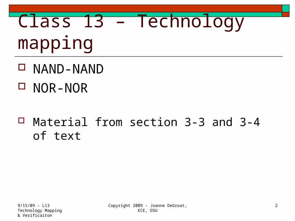
Class 13 – Technology mapping NAND-NAND NOR-NOR
Material from section 3-3 and 3-4 of text

Why does this matter? So far the minimization techniques have taught
us how to reduce to AND-OR or OR-AND gate circuits.
However, in MOS technology an AND gate is not directly implementable. A NAND gate is so an AND would be implemented by using an NAND followed by and inverter.
A NOR gate is also implementable so an OR gate is implemented by a NOR gate followed by and inverter.
9/15/09 - L13 Technology Mapping & Verificaiton
Copyright 2009 - Joanne DeGroat, ECE, OSU 3
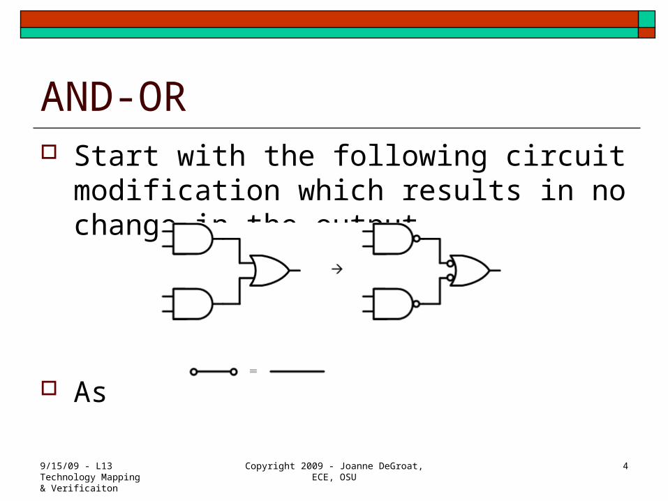
AND-OR Start with the following circuit modification
which results in no change in the output.
As
9/15/09 - L13 Technology Mapping & Verificaiton
Copyright 2009 - Joanne DeGroat, ECE, OSU 4

What is that gate? An inverted input OR gate?
9/15/09 - L13 Technology Mapping & Verificaiton
Copyright 2009 - Joanne DeGroat, ECE, OSU 5
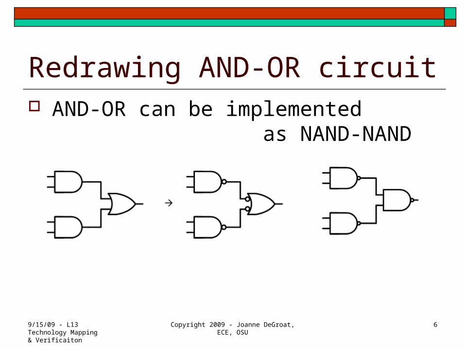
Redrawing AND-OR circuit AND-OR can be implemented
as NAND-NAND
9/15/09 - L13 Technology Mapping & Verificaiton
Copyright 2009 - Joanne DeGroat, ECE, OSU 6
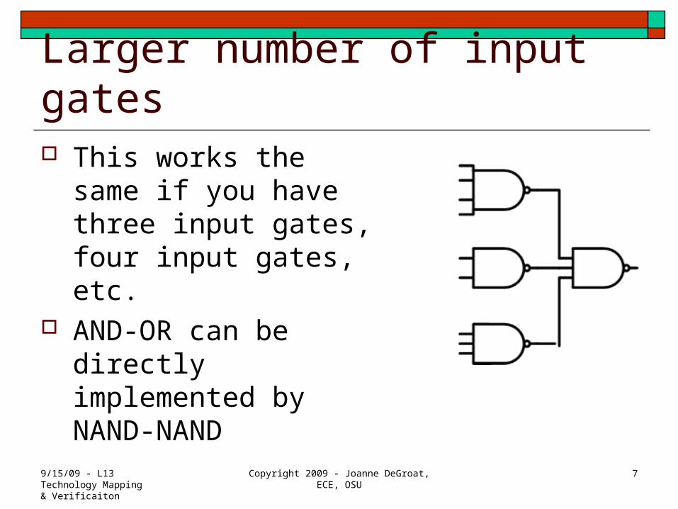
Larger number of input gates This works the same if
you have three input gates, four input gates, etc.
AND-OR can be directly implemented by NAND-NAND
9/15/09 - L13 Technology Mapping & Verificaiton
Copyright 2009 - Joanne DeGroat, ECE, OSU 7
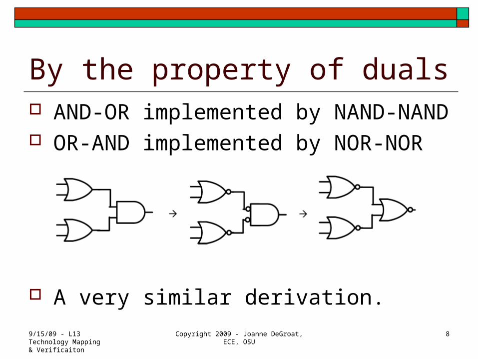
By the property of duals AND-OR implemented by NAND-NAND OR-AND implemented by NOR-NOR
A very similar derivation.
9/15/09 - L13 Technology Mapping & Verificaiton
Copyright 2009 - Joanne DeGroat, ECE, OSU 8

Inverter modifications Circuit simplifications by manipulation of
inverters. Canceling Pushing through a dot.
9/15/09 - L13 Technology Mapping & Verificaiton
Copyright 2009 - Joanne DeGroat, ECE, OSU 9

Actual implementation Today, the CAD tools often isolate you from
much of this. However, because of the implementation
specifics of reconfigurable hardware you need to know this as you often have to slightly modify how a circuit is implemented. Redrive a signal Gate types that are available.
9/15/09 - L13 Technology Mapping & Verificaiton
Copyright 2009 - Joanne DeGroat, ECE, OSU 10

The final step – Verification. Verification plays a vital role in insuring that
a faulty design is not implemented. Today, most digital designs are done in an
HDL. (Hardware Description Language)
Manual analysis – Through truth tables and hand simulation through a gate diagram.
9/15/09 - L13 Technology Mapping & Verificaiton
Copyright 2009 - Joanne DeGroat, ECE, OSU 11

Automated Use an HDL simulation system Use a system such a XILINX or ALTERA HDL code on next slide
9/15/09 - L13 Technology Mapping & Verificaiton
Copyright 2009 - Joanne DeGroat, ECE, OSU 12

HDL code for the equations ENTITY BCD_to_E3 IS
PORT(A,B,C,D : IN BIT; W,X,Y,Z : OUT BIT);END BCD_to_E3;
ARCHITECTURE one OF BCD_to_E3 ISBEGIN W <= A or (B and C) or (B and D); X <= (not B and C) or (not B and D) or (B and not C and not D); Y <= (C and D) or not(C or D); Z <= not D;END one;
Very readable!!
9/15/09 - L13 Technology Mapping & Verificaiton
Copyright 2009 - Joanne DeGroat, ECE, OSU 13

Test Stimuli Can create a testbench to apply stimulus to
the design.
9/15/09 - L13 Technology Mapping & Verificaiton
Copyright 2009 - Joanne DeGroat, ECE, OSU 14
ENTITY test IS END test; library lib261; ARCHITECTURE one OF test IS signal A,B,C,D,W,X,Y,Z : BIT; COMPONENT conv PORT(A,B,C,D : IN BIT; W,X,Y,Z : OUT BIT); END COMPONENT; FOR ALL : conv USE ENTITY lib261.bcd_to_e3(one); BEGIN c0: conv PORT MAP(A,B,C,D,W,X,Y,Z);
PROCESS BEGIN A <= '0'; B<= '0'; C<= '0'; D<= '0'; WAIT FOR 50 NS; A <= '0'; B<= '0'; C<= '0'; D<= '1'; WAIT FOR 50 NS; A <= '0'; B<= '0'; C<= '1'; D<= '0'; WAIT FOR 50 NS; A <= '0'; B<= '0'; C<= '1'; D<= '1'; WAIT FOR 50 NS; A <= '0'; B<= '1'; C<= '0'; D<= '0'; WAIT FOR 50 NS; A <= '0'; B<= '1'; C<= '0'; D<= '1'; WAIT FOR 50 NS; A <= '0'; B<= '1'; C<= '1'; D<= '0'; WAIT FOR 50 NS; A <= '0'; B<= '1'; C<= '1'; D<= '1'; WAIT FOR 50 NS; A <= '1'; B<= '0'; C<= '0'; D<= '0'; WAIT FOR 50 NS; A <= '1'; B<= '0'; C<= '0'; D<= '1'; WAIT FOR 50 NS; A <= '1'; B<= '0'; C<= '1'; D<= '0'; WAIT FOR 50 NS; A <= '1'; B<= '0'; C<= '1'; D<= '1'; WAIT FOR 50 NS; A <= '1'; B<= '1'; C<= '0'; D<= '0'; WAIT FOR 50 NS; A <= '1'; B<= '1'; C<= '0'; D<= '1'; WAIT FOR 50 NS; A <= '1'; B<= '1'; C<= '1'; D<= '0'; WAIT FOR 50 NS; A <= '1'; B<= '1'; C<= '1'; D<= '1'; WAIT FOR 50 NS; WAIT; END PROCESS; END one;

And the resulting simulation The
window showing simulation results
9/15/09 - L13 Technology Mapping & Verificaiton
Copyright 2009 - Joanne DeGroat, ECE, OSU 15

Just the waveform The
waveform as a .jpg file
9/15/09 - L13 Technology Mapping & Verificaiton
Copyright 2009 - Joanne DeGroat, ECE, OSU 16

Class 13 assignment Covered sections 3-3 and 3-4 Problems for hand in
3-16 Problems for practice
3-15, 3-17, 3-20
Reading for next class: sections 3-5 and 3-6
9/15/09 - L13 Technology Mapping & Verificaiton
Copyright 2009 - Joanne DeGroat, ECE, OSU 17