82547gi/82547ei gigabit ethernet controller - intel · —caches up to 64 packet descriptors in a...
TRANSCRIPT
82547GI/82547EI Gigabit Ethernet ControllerNetworking Silicon
Datasheet
Product Features
CSA Port— PCI-X revision 1.0a, up to 133 MHz— Uses dedicated port for client LAN controller
directly on MCH device— High-speed interface with twice the peak
bandwidth of 32-bit, 33 MHz PCI bus— PCI power management registers by MCH
MAC Specific— Optimized transmit and receive queues— IEEE 802.3x-compliant flow-control support
with software-controllable thresholds— Caches up to 64 packet descriptors in a single
burst— Programmable host memory receive buffers
(256 B to 16 KB) and cache line size (16 B to 256 B)
— Wide, optimized internal data path architecture
— 40 KB configurable Transmit and Receive FIFO buffers
— Descriptor ring management hardware for transmit and receive
— Optimized descriptor fetching and write-back mechanisms
— Mechanism available for reducing interrupts generated by transmit and receive operations
— Support for transmission and reception of packets up to 16 KB
PHY Specific— Integrated for 10/100/1000 Mb/s full- and
half-duplex operation— IEEE 802.3ab Auto-Negotiation and PHY
compliance and compatibility
— State-of-the-art DSP architecture implements digital adaptive equalization, echo and cross-talk cancellation
— PHY cable correction and diagnostics—Automatic detection of cable lengths
and MDI vs. MDI-X cable at all speeds Host Off-Loading
— Transmit and receive IP, TCP, and UDP checksum off-loading capabilities
— Transmit TCP segmentation and advanced packed filtering
— IEEE 802.1Q VLAN tag insertion and stripping and packet filtering for up to 4096 VLAN tags
— Jumbo frame support up to 16 KB— Intelligent Interrupt generation (multiple
packets per interrupt) Manageability
— On-chip SMBus 2.0 port— ASF 1.0 and 2.0— Compliance with PCI Power Management
v1.1/ACPI v2.0— Wake on LAN* (WoL) support
Additional Device— Four programmable LED outputs— On-chip power regulator control circuitry— BIOS LAN Disable pin— JTAG (IEEE 1149.1) Test Access Port built
in silicon Lead-freea 196-pin Ball Grid Array (BGA).
Devices that are lead-free are marked with a circled “e1” and have the product code: LUxxxxxx.
a. This device is lead-free. That is, lead has not been intentionally added, but lead may still exist as an impurity at <1000 ppm. The Material Declaration Data Sheet, which includes lead impurity levels and the concentration of other Restriction on Hazardous Substances (RoHS)-banned materials, is available at: ftp://download.intel.com/design/packtech/material_content_IC_Package.pdf#pagemode=bookmarksIn addition, this device has been tested and conforms to the same parametric specifications as previous versions of the device.For more information regarding lead-free products from Intel Corporation, contact your Intel Field Sales represen-tative
Revision 2.1November 2004
ii
Information in this dproperty rights is grwhatsoever, and Intfitness for a particulintended for use in
Intel may make cha
Designers must notfuture definition and
The 82547GI/82547Current characteriz
Contact your local I
Copies of documen548-4725 or by visi
Copyright © 2004 In
*Third-party brands
Revision HistoryDate Revision Notes
Aug 2003 2.0 Non-classified release.
Nov 2004 2.1 • Added Architecture Overview chapter.• Update signal names to match Design Guide and EEPROM Map and
Programming Application Note.• Updated lead-free information.• Added information about migrating from a 2-layer 0.36 mm wide-trace
substrate to a 2-layer 0.32 mm wide-trace substrate. Refer to the sec-tion on Package and Pinout Information.
• Added statement that no changes to existing soldering processes are needed for the 2-layer 0.32 mm wide-trace substrate change in the sec-tion describing “Package Information”.
Datasheet
ocument is provided in connection with Intel products. No license, express or implied, by estoppel or otherwise, to any intellectual anted by this document. Except as provided in Intel's Terms and Conditions of Sale for such products, Intel assumes no liability el disclaims any express or implied warranty, relating to sale and/or use of Intel products including liability or warranties relating to ar purpose, merchantability, or infringement of any patent, copyright or other intellectual property right. Intel products are not medical, life saving, or life sustaining applications.
nges to specifications and product descriptions at any time, without notice.
rely on the absence or characteristics of any features or instructions marked "reserved" or "undefined." Intel reserves these for shall have no responsibility whatsoever for conflicts or incompatibilities arising from future changes to them.
EI may contain design defects or errors known as errata which may cause the product to deviate from published specifications. ed errata are available on request.
ntel sales office or your distributor to obtain the latest specifications and before placing your product order.
ts which have an ordering number and are referenced in this document, or other Intel literature may be obtained by calling 1-800-ting Intel's website at http://www.intel.com.
tel Corporation
and names are the property of their respective owners.
Networking Silicon —82547GI(EI)
Contents1.0 Introduction.........................................................................................................................1
1.1 Document Scope...................................................................................................11.2 Reference Documents...........................................................................................21.3 Product Codes.......................................................................................................2
2.0 Architectural Overview .......................................................................................................32.1 Internal Architecture Block Diagram......................................................................32.2 Internal MAC Architecture Block Diagram.............................................................42.3 Integrated 10/100/1000 Mbps PHY .......................................................................52.4 CSA Controller Interface .......................................................................................5
3.0 Signal Descriptions.............................................................................................................73.1 Signal Type Definitions..........................................................................................73.2 CSA Port Interface ................................................................................................7
3.2.1 CSA Data, Strobe and Control Signals ....................................................73.2.2 CSA Termination Signals .........................................................................73.2.3 System Signals.........................................................................................83.2.4 Power Management Signals ....................................................................83.2.5 SMB Signals.............................................................................................8
3.3 EEPROM and Serial Flash and Interface Signals .................................................93.4 Miscellaneous Signals...........................................................................................9
3.4.1 LED Signals..............................................................................................93.5 Other Signals ........................................................................................................9
3.5.1 Crystal Signals .......................................................................................103.5.2 Analog Signals .......................................................................................10
3.6 Test Interface Signals..........................................................................................103.7 Power Supply Connections .................................................................................11
3.7.1 Digital and Analog Supplies ...................................................................113.7.2 Grounds, Reserved Pins and No Connects ...........................................113.7.3 Voltage Regulation Control Signals........................................................11
4.0 Voltage, Temperature, and Timing Specifications............................................................134.1 Absolute Maximum Ratings.................................................................................134.2 Recommended Operating Conditions .................................................................144.3 DC Specifications ................................................................................................144.4 AC Characteristics...............................................................................................184.5 Timing Specifications ..........................................................................................19
4.5.1 Link Interface Timing ..............................................................................194.5.2 EEPROM Interface.................................................................................19
5.0 Package and Pinout Information ......................................................................................215.1 Package Information ...........................................................................................215.2 Thermal Specifications ........................................................................................235.3 Pinout Information ...............................................................................................245.4 Visual Pin Assignments.......................................................................................33
Datasheet iii

82547GI(EI)— Networking Silicon
Note: This page intentionally left blank.
iv Datasheet
Networking Silicon — 82547GI(EI)
1.0 Introduction
The Intel® 82547GI(EI) Gigabit Ethernet Controller is a single, compact component with integrated Gigabit Ethernet Media Access Control (MAC) and physical layer (PHY) functions. This device uses the Communications Streaming Architecture (CSA) port of the Intel® 865 and Intel® 875 Chipset. The Intel® 82547GI(EI) allows for a Gigabit Ethernet implementation in a very small area that is footprint compatible with current generation 10/100 Mbps Fast Ethernet designs.
The Intel® 82547GI(EI) integrates Intel’s fifth generation gigabit MAC design with fully integrated, physical layer circuitry to provide a standard IEEE 802.3 Ethernet interface for 1000BASE-T, 100BASE_TX, and 10BASE-T applications (802.3, 802.3u, and 802.3ab). The controller is capable of transmitting and receiving data at rates of 1000 Mbps, 100 Mbps, or 10 Mbps. In addition to managing MAC and PHY layer functions, the controller uses dedicated CSA port capability with a theoretical bandwidth of 266 MB/s.
The 82547GI(EI) on-board System Management Bus (SMB) port enables network manageability implementations required by information technology personnel for remote control and alerting via the LAN. With SMB, management packets can be routed to or from a management processor. The SMB port enables industry standards, such as Intelligent Platform Management Interface (IPMI) and Alert Standard Forum (ASF) 2.0, to be implemented using the 82547GI(EI). In addition, on-chip ASF 2.0 circuitry provides alerting and remote control capabilities with standardized interfaces.
The 82547GI(EI) Gigabit Ethernet Controller with CSA is designed for high performance and low memory latency. The CSA port architecture is invisible to both system software and the operating system, allowing a conventional PCI-like configuration.
Wide internal data paths eliminate performance bottlenecks by efficiently handling large address and data words. The 82547GI(EI) controller includes advanced interrupt handling features. The 82547GI(EI) uses efficient ring buffer descriptor data structures, with up to 64 packet descriptors cached on chip. A large 40 KB on-chip packet buffer maintains superior performance. In addition, by using hardware acceleration, the controller offloads tasks from the host, such as TCP/UDP/IP checksum calculations and TCP segmentation.
The 82547GI(EI) is packaged in a 15 mm X 15 mm, 196-ball grid array and is footprint compatible with 82562EZ/82562EX Platform LAN Connect devices.
1.1 Document Scope
The 82547GI(EI) is the original device and is now in being manufactured in a B0 stepping. The 82547GI is pin compatible and is a B1 stepping of the same product, however a different Intel software driver is required. This document contains datasheet specifications for the 82547GI(EI) Gigabit Ethernet Controller, including signal descriptions, DC and AC parameters, packaging data, and pinout information.
Datasheet 1

82547GI(EI) — Networking Silicon
1.2 Reference Documents
This document assumes that the designer is acquainted with high-speed design and board layout techniques. The following documents provide application information:
• 82562EZ(EX)/82547GI(EI) Dual Footprint Design Guide. Intel Corporation.
• 82547GI(EI)/82541(PI/GI/EI) EEPROM Map and Programming Information Guide. Intel Corporation.
• PCI Local Bus Specification, Revision 2.3. PCI Special Interest Group (SIG).
• PCI Bus Power Management Interface Specification, Revision 1.1. PCI Special Interest Group (SIG).
• IEEE Standard 802.3, 2000 Edition. Incorporates various IEEE standards previously published separately. Institute of Electrical and Electronic Engineers (IEEE).
• Intel Ethernet Controllers Timing Device Selection Guide. Intel Corporation.
Software driver developers should contact their local Intel representatives for programming information.
1.3 Product Codes
The product ordering codes for the 82547GI(EI) controller are:
• GD82547GI
• GD82547EI
• LU82547GI
• LU82547EI
2 Datasheet
Networking Silicon — 82547GI(EI)
2.0 Architectural Overview
2.1 Internal Architecture Block Diagram
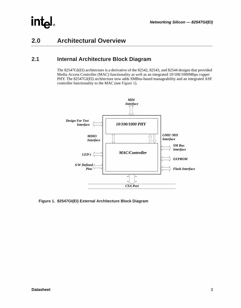
The 82547GI(EI) architecture is a derivative of the 82542, 82543, and 82544 designs that provided Media Access Controller (MAC) functionality as well as an integrated 10/100/1000Mbps copper PHY. The 82547GI(EI) architecture now adds SMBus-based manageability and an integrated ASF controller functionality to the MAC (see Figure 1).
Figure 1. 82547GI(EI) External Architecture Block Diagram
CSA Port
S/W Defined Pins
MDI Interface
Design For Test Interface
LED's EEPROM
Flash Interface
SM Bus Interface
MAC/Controller
10/100/1000 PHY
MDIO Interface
GMII /MII Interface
Datasheet 3
82547GI(EI) — Networking Silicon
2.2 Internal MAC Architecture Block Diagram
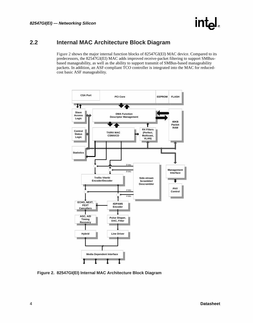
Figure 2 shows the major internal function blocks of 82547GI(EI) MAC device. Compared to its predecessors, the 82547GI(EI) MAC adds improved receive-packet filtering to support SMBus-based manageability, as well as the ability to support transmit of SMBus-based manageability packets. In addition, an ASF-compliant TCO controller is integrated into the MAC for reduced-cost basic ASF manageability.
Figure 2. 82547GI(EI) Internal MAC Architecture Block Diagram
VLAN
PCI Core EEPROM FLASH
SlaveAccessLogic
DMA FunctionDescriptor Management
ControlStatusLogic
Statistics
TX/RX MACCSMA/CD
40KBPacketRAM
RX Filters(Perfect,
Multicast,VLAN)
ManagementInterface
PHYControl
Side-streamScrambler/
Descrambler
Media Dependent Interface
ECHO, NEXT,FEXT
Cancellers
Trellis ViterbiEncoder/Decoder
Line DriverHybrid
Pulse Shaper,DAC, Filter
AGC, A/DTiming
Recovery
4DPAM5Encoder
8 bits
8 bits
4 bits
4 bits
CSA Port
4 Datasheet

Networking Silicon — 82547GI(EI)
2.3 Integrated 10/100/1000 Mbps PHY
The 82547GI(EI) contains an integrated 10/100/1000Mbps-capable Copper PHY. This PHY communicates with the MAC controller using a standard GMII/MII interface internal to the component to transfer transmit and receive data. A standard MDIO interface, accessible to software via MAC control registers, is used to configure and monitor the PHY operation.
2.4 CSA Controller Interface
The 82547EI Gigabit Ethernet Controller connects to the motherboard chipset through a Communications Streaming Architecture (CSA) port. CSA is designed for low memory latency and higher performance than a comparable PCI interface.
The Communications Streaming Architecture is derived from the Intel Hub Architecture. The 82547GI(EI) controller’s CSA port consists of 11 data and control signals, two strobes, a 66 MHz clock, and driver compensation resistor connections. The CSA port has a theoretical bandwidth of 266 MB/s — approximately twice the peak bandwidth of a 32-bit 33 MHz PCI bus.
Datasheet 5

82547GI(EI) — Networking Silicon
Note: This page intentionally left blank.
6 Datasheet
Networking Silicon — 82547GI(EI)
3.0 Signal Descriptions
3.1 Signal Type Definitions
The signals of the 82547GI(EI) controller are electrically defined as follows:
3.2 CSA Port Interface
When the Reset signal (RST#) is asserted, the 82547GI(EI) does not drive the CSA Port interface. The Power Management Event signal (PME#) can still be activated, subject to programming.
3.2.1 CSA Data, Strobe and Control Signals
3.2.2 CSA Termination Signals
Name Definition
I Input. Standard input only digital signal.
O Output. Standard output only digital signal.
TS Tri-state. Bi-directional three-state digital input/output signal.
OD
Open Drain. Wired-OR with other agents.The signaling agent asserts the OD signal, but the signal is returned to the inactive state by a weak pull-up resistor. The pull-up resistor may require two or three clock periods to fully restore the signal to the de-asserted state.
A Analog. PHY analog data signal.
P Power. Power connection, voltage reference, or other reference connection.
Symbol Type Name and Function
CI[10:0] TSCommunications Streaming Architecture Interface. High-speed, 11-pin interface for sending/receiving packet data to the GMCH (Memory Control Hub). The CSA port is implemented with Invert Gunning Transceiver Logic (IGTL)
CI_CLK ICSA Interface Clock. The clock signal provides timing for all transactions on the CSA port and is an input to the 82547GI(EI) device. Timing parameters are defined with respect to this reference.
Symbol Type Name and Function
CI_ RCOMP P CSA Compensation Resistor. Connect a 30 ohm 1% resistor between this pin and the
1.2 V supply for I/O circuit compensation (process, temperature, voltage).
CI_SWING P CSA Swing Voltage. Biased to 0.8 V reference with an external voltage divider network.
CI_VREF P CSA Voltage Reference. Biased to 0.35 V reference with an external voltage divider network.
Datasheet 7
82547GI(EI) — Networking Silicon
3.2.3 System Signals
3.2.4 Power Management Signals
3.2.5 SMB Signals
Symbol Type Name and Function
RST# I
Reset. When the Reset signal is asserted, the CSA port is inactivated and all input signals are ignored. The controller can still activate the Power Management Event signal (PME#) and PME# context is preserved according to power management settings.
Symbol Type Name and Function
LAN_ PWR_ GOOD
I
Power Good (Power-on Reset). The Power Good signal is used to indicate that stable power is available for the 82547GI(EI). When the signal is low, the 82547GI(EI) holds itself in reset state. LAN_PWR_GOOD acts as a master reset of the entire chip. It is level sensitive. While deasserted, the registers are reset and the CSA interface is quiet
PME# OD
Power Management Event. The 82547GI(EI) device drives this signal low when it receives a wake-up event and either the PME Enable bit in the Power Management Control/Status Register or the Advanced Power Management Enable (APME) bit of the Wake-up Control Register (WUC) is 1b.
AUX_PWR I Auxiliary Power. If the Auxiliary Power signal is high, then auxiliary power is available and the 82547GI(EI) device should support the D3cold power state.
Symbol Type Name and Function
SMBCLK I/O SMB Clock. The SMB Clock signal is an open drain signal for serial SMB interface.
SMBDATA I/O SMB Data. The SMB Data signal is an open drain signal for serial SMB interface.
SMB_ ALERT# I/O SMB Alert. The SMB Alert signal is open drain for serial SMB interface. In ASF mode, this signal acts as POWER GOOD input.
8 Datasheet

Networking Silicon — 82547GI(EI)
3.3 EEPROM and Serial Flash and Interface Signals
3.4 Miscellaneous Signals
3.4.1 LED Signals
3.5 Other Signals
Symbol Type Name and Function
EEMODE I
EEPROM Mode. The EEPROM Mode pin is used to select the interface and source of the EEPROM used to initialize the device. For a MIcrowire* EEPROM on the standard EEPROM pins, tie this pin to ground with a pull-down resistor. For an SPI* EEPROM, use a pull-up resistor.
EEDI O EEPROM Data Input. The EEPROM Data Input pin is used for output to the memory device.
EEDO I EEPROM Data Output. The EEPROM Data Output pin is used for input from the memory device. The EEDO includes an internal pull-up resistor.
EECS O EEPROM Chip Select. The EEPROM Chip Select signal is used to enable the device.
EE_SK OEEPROM Serial Clock. The EEPROM Shift Clock provides the clock rate for the EEPROM interface. The clock rate of the serial FLASH interface is approximately 1 MHz for Microwire* and 2 MHz for SPI* EEPROMs
FLSH_CE# O FLASH Chip Enable Output. Used to enable FLASH device.
FLSH_SCK O FLASH Serial Clock Output.
FLSH_SI O FLASH Serial Data Input. This pin is an output to the memory device.
FLSH_SO/ LAN_ DISABLE#
IFLASH Serial Data Output/LAN Disable. Input from an external FLASH memory. Alternatively, it can be used to disable the LAN port from a system GP (General Purpose) port under BIOS control. This pin has an internal pull-up device.
Symbol Type Name and Function
LED0 / LINK_UP# O LED0 / LINK Up. Programmable LED indication. Defaults to indicate link connectivity..
LED1 / ACTIVITY# O LED1 / Activity. Programmable LED indication. Defaults to flash to indicate transmit or receive activity..
LED2 / LINK100# O LED2 / LINK 100. Programmable LED indication. Defaults to indicate link at 100 Mbps.
LED3 / LINK1000# O LED3 / LINK 1000. Programmable LED indication. Defaults to indicate link at 1000 Mbps.
Symbol Type Name and Function
SDP[3:0] TS
Software Defined Pin. The Software Defined Pins are programmable with respect to input and output capability. SDP[3:2] can be optionally configured as interrupt inputs. SDP signals default to inputs upon power-up but can be configured differently by the EEPROM.
Datasheet 9

82547GI(EI) — Networking Silicon
3.5.1 Crystal Signals
3.5.2 Analog Signals
3.6 Test Interface Signals
Symbol Type Name and Function
XTAL1 I Crystal One. The Crystal One pin is a 25 MHz +/- 30 ppm input signal. It should be connected to a crystal, and the other end of the crystal should be connected to XTAL2.
XTAL2 O Crystal Two. Crystal Two is the output of an internal oscillator circuit used to drive a crystal into oscillation.
Symbol Type Name and Function
MDI[0]+/- A
Media Dependent Interface [0]. 1000BASE-T: In MDI configuration, MDI[0]+/- corresponds to BI_DA+/-, and in MDI-X configuration, MDI[0]+/- corresponds to BI_DB+/-.100BASE_TX: In MDI configuration, MDI[0]+/- is used for the transmit pair, and in MDI-X configuration, MDI[0]+/- is used for the receive pair.10BASE-T: In MDI configuration, MDI[0]+/- is used for the transmit pair, and in MDI-X configuration, MDI[0]+/- is used for the receive pair.
MDI[1]+/- A
Media Dependent Interface [1]. 1000BASE-T: In MDI configuration, MDI[1]+/- corresponds to BI_DB+/-, and in MDI-X configuration, MDI[1]+/- corresponds to BI_DA+/-.100BASE_TX: In MDI configuration, MDI[1]+/- is used for the receive pair, and in MDI-X configuration, MDI[1]+/- is used for the transit pair.10BASE-T: In MDI configuration, MDI[1]+/- is used for the receive pair, and in MDI-X configuration, MDI[1]+/- is used for the transit pair.
MDI[2]+/- A
Media Dependent Interface [2]. 1000BASE-T: In MDI configuration, MDI[2]+/- corresponds to BI_DC+/-, and in MDI-X configuration, MDI[2]+/- corresponds to BI_DD+/-.100BASE_TX: Unused.10BASE-T: Unused.
MDI[3]+/- A
Media Dependent Interface [3]. 1000BASE-T: In MDI configuration, MDI[3]+/- corresponds to BI_DD+/-, and in MDI-X configuration, MDI[3]+/- corresponds to BI_DC+/-.100BASE_TX: Unused.10BASE-T: Unused.
Symbol Type Name and Function
JTAG_TCK I JTAG Test Access Port Clock.
JTAG_TDI I JTAG Test Access Port Test Data In.
JTAG_TDO O JTAG Test Access Port Test Data Out.
JTAG_TMS I JTAG Test Access Port Mode Select.
10 Datasheet

Networking Silicon — 82547GI(EI)
3.7 Power Supply Connections
3.7.1 Digital and Analog Supplies
3.7.2 Grounds, Reserved Pins and No Connects
3.7.3 Voltage Regulation Control Signals
JTAG_TRST# IJTAG Test Access Port Reset. This is an active low reset signal for JTAG. This signal should be terminated using a pull-down resistor to ground. It must not be left unconnected.
TEST I Factory Test Pin. Connect directly to ground for normal operation.
IEEE_TEST+/- A IEEE Test Pins. Differential output used for IEEE PHY conformance testing.
Symbol Type Name and Function
3.3V P 3.3 V I/O Power Supply.
1.8V P 1.8 V Analog Power Supply.
1.2V P 1.2 V Power Supply. For analog, CSA, and digital circuits.
Symbol Type Name and Function
GND P Ground. Connects to analog or digital circuits.
RSVD_ 3.3V P Reserved, 3.3V. This pin is reserved by Intel and may have factory test functions. For
normal operation, connect to 3.3V.
RSVD_ GND P Reserved, Ground This pin is reserved by Intel and may have factory test functions.
For normal operation, connect to ground.
RSVD_ NC PReserved, No Connect. This pin is reserved by Intel and may have factory test functions. For normal operation, do not connect any circuitry to these pins. Do not connect pull-up or pull-down resistors.
NC P No Connect. This pin is not connected internally.
Symbol Type Name and Function
CTRL12 A
1.2V Control. LDO voltage regulator output to drive external PNP pass transistor. If 1.2V is already present in the system, leave output unconnected. To achieve optimal D3 power consumption, leave the output unconnected and use a high-efficiency external switching regulator.
CTRL18 A
1.8V Control. LDO voltage regulator output to drive external PNP pass transistor. If 1.8V is already present in the system, leave output unconnected. To achieve optimal D3 power consumption, leave the output unconnected and use a high-efficiency external switching regulator.
Symbol Type Name and Function
Datasheet 11

82547GI(EI) — Networking Silicon
Note: This page intentionally left blank.
12 Datasheet

Networking Silicon — 82547GI(EI)
4.0 Voltage, Temperature, and Timing Specifications
4.1 Absolute Maximum Ratings
Table 1. Absolute Maximum Ratingsa
a. Maximum ratings are referenced to ground (VSS). Permanent device damage is likely to occur if the ratings in this table are exceeded. These values should not be used as the limits for normal device operations.
Symbol Parameter Min Max Unit
VDD (3.3) DC supply voltage on 3.3 V pins with respect to VSS VSS - 0.5 4.6 V
VDD (1.8) DC supply voltage on 1.8 V pins with respect to VSS VSS - 0.5 2.5 or
VDD (1.8) + 0.5b
b. The maximum value is the lesser value of 2.5V or VDD(2.5) + 0.5 V. This specification applies to biasing the device to a steady state for an indefinite duration. During normal device power-up, explicit power sequencing is not required.
V
VDD (1.2) DC supply voltage on 1.2V pins with respect to VSS VSS - 0.5 1.7 or
VDD (1.5) + 0.5c
c. The maximum value is the lesser value of 1.7V or VDD(2.5) + 0.5 V.
V
VDD DC supply voltage VSS - 0.5 4.6 V
VI / VO LVTTL input voltage VSS - 0.5 4.6 V
IO
DC output current (by cell type):IOL = 2 mAIOL = 4 mAIOL = 8 mAIOL - 12 mA
5102030
mA
TSTG Storage temperature range -40 125 C
ESD per MIL_STD-883 Test Method 3015, Specification 2001V Latchup Over/Undershoot: 150 mA, 125 C
VDD overstress: VDD(3.3)(7.2 V) V
Datasheet 13

82547GI(EI) — Networking Silicon
4.2 Recommended Operating Conditions
4.3 DC Specifications
Table 4. Power Specifications - D0a
Table 2. Recommended Operating Conditions a
a. Sustained operation of the device at conditions exceeding these values, even if they are within the absolute maximum rating limits, might result in unreliable operation or permanent damage.
Symbol Parameter Min Max Unit
VDD (3.3) DC supply voltage on 3.3 V pins 3.0 3.6 V
VDD (1.8) DC supply voltage on 1.8 V pinsbc
b. It is recommended for 3.3 V pins to be of a value greater than 1.8 V pins, with a value greater than 1.2 V pins, during power-up (3.3 V pins > 1.8 V pins > 1.2 V pins). However, voltage sequencing is not a strict requirement if the power supply ramp is faster than approximately 20 ms.
c. Includes both the DC component of the voltage and the AC ripple that may be present when using the internal voltage regulator control circuits with PNP pass transistors.
1.71 1.89 V
VDD (1.2) DC supply voltage on 1.2 V pinsbc 1.14 1.26 V
tR / tF Input rise/fall time (normal input) 0 200 ns
tr/tf input rise/fall time (Schmitt input) 0 10 ms
TA Operating temperature range (ambient) 0 55 °C
TJ Junction temperature ≤125 °C
Table 3. DC Characteristics
Symbol Parameter Condition Min Typ Max Units
VDD (3.3) DC supply voltage on 3.3 V pins 3.00 3.3 3.60 V
VDD (1.8) DC supply voltage on 1.8 V pins 1.71 1.8 1.89 V
VDD (1.2) DC supply voltage on 1.2 V pins 1.14 1.5 1.26 V
D0a
Unplugged No Link @10 Mbps @100Mbps @ 1000 Mbps
Typ Icc (mA)a
Max Icc (mA)b
Typ Icc (mA)a
Max Icc (mA)b
Typ Icc (mA)a
Max Icc (mA)b
Typ Icc (mA)a
Max Icc (mA)b
3.3V 8 19 4 5 8 10 8 10
14 Datasheet

Networking Silicon — 82547GI(EI)
Table 5. Power Specifications - D3cold
1.8V 21 25 10 95 115 120 320 325
1.2V 55 65 145 160 160 170 440 485
Total Device Power
135 150 435 1.1W 1.2W
a. Typical conditions: operating temperature (TA) = 25 C, nominal voltages, moderate network traffic at full duplex, and PCI 33 MHz system interface.
b. Maximum conditions: minimum operating temperature (TA) values, maximum voltage values, con-tinuous network traffic at full duplex, and PCI 33 MHz system interface.
D3cold - wake-up enabled D3cold-wake disabledunplugged link @10 Mbps @100Mbps
Typ Icc (mA)a
a. Typical conditions: operating temperature (TA) = 25 C, nominal voltages, moderate network traffic at full duplex, and PCI 33 MHz system interface.
Max Icc (mA)b
b. Maximum conditions: minimum operating temperature (TA) values, maximum voltage values, con-tinuous network traffic at full duplex, and PCI 33 MHz system interface.
Typ Icc (mA)a
Max Icc (mA)b
Typ Icc (mA)a
Max Icc (mA)b
Typ Icc (mA)a
Max Icc (mA)b
3.3V 8 10 8 10 8 10 8 16
1.8V 21 25 27 30 115 120 22 25
1.2V 50 55 70 80 115 130 45 50
Total Device Power
125 160 380 125
D0a
Unplugged No Link @10 Mbps @100Mbps @ 1000 Mbps
Typ Icc (mA)a
Max Icc (mA)b
Typ Icc (mA)a
Max Icc (mA)b
Typ Icc (mA)a
Max Icc (mA)b
Typ Icc (mA)a
Max Icc (mA)b
Datasheet 15

82547GI(EI) — Networking Silicon
Table 6. Power Specifications - D(r) Uninitialized
Table 7. Power Specifications - Complete Subsystem
D(r) Uninitialized (FLSH_SO/LAN_DISABLE # = 0)
Typ Icc (mA) Max Icc (mA)
3.3V 20 25
1.8V 1 1
1.2V 8 8
Total Device Power
80
Complete Subsystem (Reference Design) Including Magnetics, LED, REgulator Circuits
D3cold - wake disabled
D3cold wake-enabled @
10MbpsD0 @100Mbps
activeD0 @ 1000Mbps
active
Typ Icc (mA)a
a. Typical conditions: operating temperature (TA) = 25 C, nominal voltages, moderate network traffic at full du-plex, and PCI 33 MHz system interface.
Max Icc (mA)b.
b. Maximum conditions: minimum operating temperature (TA) values, maximum voltage values, continuous network traffic at full duplex, and PCI 33 MHz system interface.
Typ Icc (mA)a
Max Icc (mA)b
Typ Icc (mA)a
Max Icc (mA)b
Typ Icc (mA)a
Max Icc (mA)b
3.3V 8 10 13 15 18 20 13 15
1.8V 22 25 35 40 140 145 415 420
1.2V 45 50 65 80 115 130 440 485
Subsystem 3.3V Current 125 65 145 710
Table 8. I/O Characteristics (Sheet 1 of 2)
Symbol Parameter Condition Min Typ Max Units
VIH Input high voltage LVTTL 2.0 VDD(3.3) V
VIL Input low voltage LVTTL VSS 0.8 V
VT+Switching threshold: positive edge
LVTTL 1.2 2.4 V
VT-Switching threshold: negative edge
LVTTL 0.6 1.8 V
VH Schmitt trigger-hysteresis 0.3 1.5 V
16 Datasheet

Networking Silicon — 82547GI(EI)
IIN
Input current VIN = VDD(3.3) or VSS -5 5
µA
Input with pull-down resistor (50 KΩ)
VIN = VDD(3.3) 28 191
Inputs with pull-up resistor (50 KΩ)
VIN = VSS -28 -191
IOL Output low current:
• 0 <= VOUT <= 3.6V
• 0 <= VOUT <= 1.3V
• 1.3V <= VOUT <= 3.6V
100 VOUT 48 VOUT 5.7 VOUT+ 55
mA
IOHOutput high current:
• 0 <= (VDD-VOUT) <= 3.6V
• 0 <= (VDD-VOUT) <= 1.2V
• 1.2V <= (VDD-VOUT) <= 1.9V
• -74(VDD -VOUT)
• -32(VDD -VOUT)
• -1.1(VDD -VOUT)-25.2
• -1.8(VDD -VOUT)-42.7
mA
VOH
Output high voltage:
VLVTTL IOH = 0 mA VDD(3.3) -
0.1
VOLOutput low voltage: VLVTTL IOL = 0 mA 0.1
IOZ Off-state output leakage current VO = VDD or VSS -10 10 µA
IOS Output short circuit current -250 µA
CIN Input capacitancea
Input and bi-directional buffers 4 pF
COUT Output capacitance Output buffers 6 pF
a. VDD (3.3) = 0 V; TA = 25 C; f = 1 Mhz
Table 8. I/O Characteristics (Sheet 2 of 2) (Continued)
Symbol Parameter Condition Min Typ Max Units
Datasheet 17
82547GI(EI) — Networking Silicon
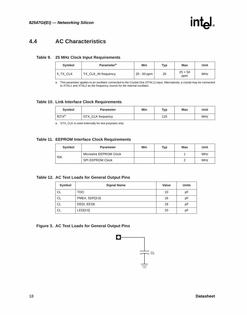
4.4 AC Characteristics
Table 9. 25 MHz Clock Input Requirements
Symbol Parametera
a. This parameter applies to an oscillator connected to the Crystal One (XTAL1) input. Alternatively, a crystal may be connected to XTAL1 and XTAL2 as the frequency source for the internal oscillator.
Min Typ Max Unit
fi_TX_CLK TX_CLK_IN frequency 25 - 50 ppm 25 25 + 50 ppm MHz
Table 10. Link Interface Clock Requirements
Symbol Parameter Min Typ Max Unit
fGTXa GTX_CLK frequency 125 MHz
a. GTX_CLK is used externally for test purposes only.
Table 11. EEPROM Interface Clock Requirements
Symbol Parameter Min Typ Max Unit
fSKMIcrowire EEPROM Clock 1 MHz
SPI EEPROM Clock 2 MHz
Table 12. AC Test Loads for General Output Pins
Symbol Signal Name Value Units
CL TDO 10 pF
CL PME#, SDP[3:0] 16 pF
CL EEDI, EESK 18 pF
CL LED[3:0] 20 pF
Figure 3. AC Test Loads for General Output Pins
CL
18 Datasheet
Networking Silicon — 82547GI(EI)
4.5 Timing Specifications
Note: Timing specifications are preliminary and subject to change. Verify with your local Intel sales office that you have the latest information before finalizing a design.
4.5.1 Link Interface Timing
4.5.2 EEPROM Interface
Table 13. Rise and Fall Times
Symbol Parameter Condition Min Max Unit
TR Clock rise time 0.8 V to 2.0 V 0.7 ns
TF Clock fall time 2.0 V to 0.8 V 0.7 ns
TR Data rise time 0.8 to 2.0 V 0.7 ns
TF Data fall time 2.0 V to 0.8 V 0.7 ns
Figure 4. Link Interface Rise/Fall Timing
Table 14. EEPROM Interface Clock Requirements
Symbol Parametera
a. The EEPROM clock is derived from a 125 MHz internal clock.
Min Typ Max Unit
TPWMicrowire EESK pulse width TPERIOD x 64 ns
SPI EESK pulse width TPERIOD x 32 ns
Table 15. EEPROM Interface Clock Requirements
Symbol Parametera
a. The EEDO setup and hold time is a function of the internal data bus clock cycle time but is referenced to O_EESK.
Min Typ Max Unit
TDOS EE_DO setup time TCYC*2 ns
TDOH EE_DO hold time 0 ns
2.0 V
0.8 V
TFTR
Datasheet 19
82547GI(EI) — Networking Silicon
Note: This page is intentionally left blank.
20 Datasheet

Networking Silicon —82547GI(EI)
5.0 Package and Pinout Information
This section describes the 82547GI(EI) device physical characteristics. The pin number-to-signal mapping is indicated beginning with Table 14.
5.1 Package Information
The 82547GI(EI) device is a 196-lead plastic ball grid array (BGA) measuring 15 mm by 15mm. The package dimensions are detailed as follows. The nominal ball pitch is 1 mm.
Note: No changes to existing soldering processes are needed for the 0.32 mm substrate change.
Figure 1. 82547GI(EI) Mechanical Specifications
Substrate change from
0.36 mm to 0.32 mm
0.32 +/-0.04
Note: All dimensions are in millimeters.
0.40 +/-0.10 Seating Plate
0.85
1.56 +/-0.1930
o
Datasheet 21

82547GI(EI)— Networking Silicon
Figure 2. 196 PBGA Package Pad Detail
As shown, the Ethernet controller package uses solder mask designed pads. The copper area is 0.60mm and the opening in the solder mask is 0.45 mm. The nominal ball sphere diameter is 0.50mm.
0.45Solder Resist Opening
0.60Metal Diameter
Detail Area
22 Datasheet
Networking Silicon —82547GI(EI)
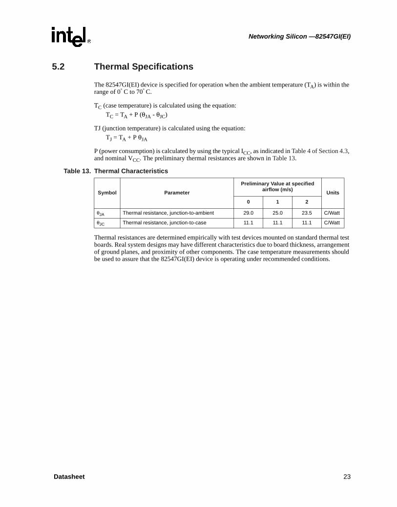
5.2 Thermal Specifications
The 82547GI(EI) device is specified for operation when the ambient temperature (TA) is within the range of 0° C to 70° C.
TC (case temperature) is calculated using the equation:TC = TA + P (θJA - θJC)
TJ (junction temperature) is calculated using the equation:TJ = TA + P θJA
P (power consumption) is calculated by using the typical ICC, as indicated in Table 4 of Section 4.3, and nominal VCC. The preliminary thermal resistances are shown in Table 13.
Thermal resistances are determined empirically with test devices mounted on standard thermal test boards. Real system designs may have different characteristics due to board thickness, arrangement of ground planes, and proximity of other components. The case temperature measurements should be used to assure that the 82547GI(EI) device is operating under recommended conditions.
Table 13. Thermal Characteristics
Symbol Parameter
Preliminary Value at specified airflow (m/s) Units
0 1 2
θJA Thermal resistance, junction-to-ambient 29.0 25.0 23.5 C/Watt
θJC Thermal resistance, junction-to-case 11.1 11.1 11.1 C/Watt
Datasheet 23

82547GI(EI)— Networking Silicon
5.3 Pinout Information
Table 14. CSA Port Signals
Signal Pin Signal Pin Signal Pin
CI[0] J1 CI[6] M1 CI_STRS L1
CI[1] J2 CI[7] N2 CL_RCOMP N3
CI[2] J3 CI[8] H3 CI_SWING P3
CI[3] K1 CI[9] G2 CI_VREF N4
CI[4] L3 CI[10] H1 CI_CLK G1
CI[5] M2 CI_STRF L2
Table 15. System Signals
Signal Pin
RST# B9
Table 16. Power Management Signals
Signal Pin Signal Pin Signal Pin
LAN_PWR_GOOD A9 AUX_PWR J12 PME# A6
Table 17. SMB Signals
Signal Pin Signal Pin Signal Pin
SMBCLK A10 SMBDATA C9 SMB_ALERT# B10
Table 18. EEPROM and Serial FLASH Interface Signals
Signal Pin Signal Pin Signal Pin
EEMODE C4 EECS P7 FLSH_SI M11
EESK M10 EEDI P10 FLSH_SCK N9
EEDO N10 FLSH_CE# M9 FLSH_SO/LAN_DISABLE# P9
Table 19. LED Signals
Signal Pin Signal Pin
LED0 / LINK_UP# A12 LED2 / LINK100# B11
LED1 / ACTIVITY# C11 LED3 / LINK1000# B12
24 Datasheet
Networking Silicon —82547GI(EI)
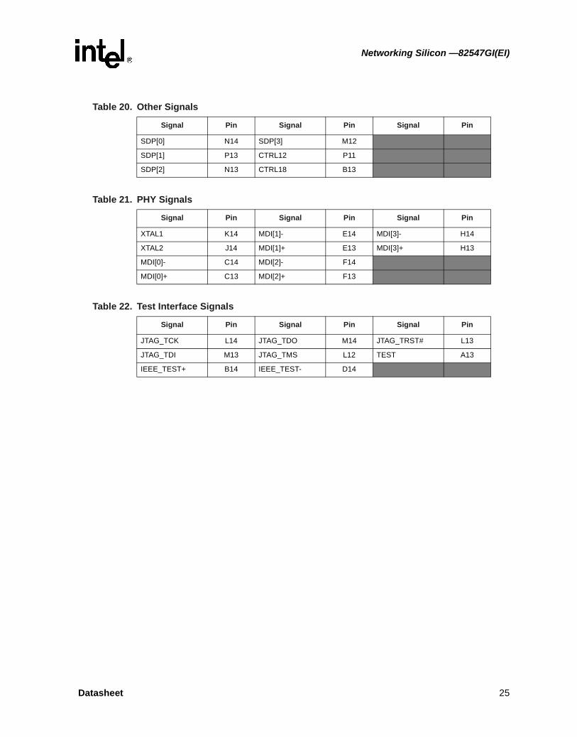
Table 20. Other Signals
Signal Pin Signal Pin Signal Pin
SDP[0] N14 SDP[3] M12
SDP[1] P13 CTRL12 P11
SDP[2] N13 CTRL18 B13
Table 21. PHY Signals
Signal Pin Signal Pin Signal Pin
XTAL1 K14 MDI[1]- E14 MDI[3]- H14
XTAL2 J14 MDI[1]+ E13 MDI[3]+ H13
MDI[0]- C14 MDI[2]- F14
MDI[0]+ C13 MDI[2]+ F13
Table 22. Test Interface Signals
Signal Pin Signal Pin Signal Pin
JTAG_TCK L14 JTAG_TDO M14 JTAG_TRST# L13
JTAG_TDI M13 JTAG_TMS L12 TEST A13
IEEE_TEST+ B14 IEEE_TEST- D14
Datasheet 25

82547GI(EI)— Networking Silicon
Table 23. Power Signals
Signal Pin Signal Pin Signal Pin
3.3V A3 1.2V G5 1.2V K5
3.3V A7 1.2V G6 1.2V K6
3.3V A11 1.2V G13 1.2V K7
3.3V E1 1.2V H4 1.2V K8
3.3V K3 1.2V H5 1.2V K9
3.3V K13 1.2V H6 1.2V K10
3.3V N6 1.2V H7 1.2V K11
3.3V N8 1.2V H8 1.2V L4
3.3V P2 1.2V H11 1.2V L5
3.3V P12 1.2V J4 1.2V L9
1.8V D11 1.2V J5 1.2V L10
1.8V D12 1.2V J6 1.2V M4
1.8V G12 1.2V J7 1.2V M5
1.8V J13 1.2V J8 1.2V N5
1.2V E11 1.2V J9
1.2V E12 1.2V J10
1.2V G4 1.2V J11
Table 24. Ground Signals
Signal Pin Signal Pin Signal Pin
GND B3 GND E9 GND G14
GND B7 GND F4 GND H2
GND C10 GND F6 GND H9
GND C12 GND F7 GND H10
GND D5 GND F8 GND K2
GND D7 GND F9 GND K12
GND D8 GND F10 GND L6
GND D13 GND F11 GND L11
GND E2 GND G7 GND M3
GND E5 GND G8 GND M6
GND E6 GND G9 GND N1
GND E7 GND G10 GND N12
GND E8 GND G11 GND P8
26 Datasheet

Networking Silicon —82547GI(EI)
Table 25. Reserved and No Connect Signals
Signal Pin Signal Pin Signal Pin Signal Pin
RSVD_3.3V K4 RSVD_ NC B4 RSVD_ NC D2 RSVD_ NC M7
RSVD_ GND D4 RSVD_ NC B5 RSVD_ NC D3 RSVD_ NC M8
RSVD_ GND D6 RSVD_ NC B6 RSVD_ NC D9 RSVD_ NC N7
RSVD_ GND E4 RSVD_ NC B8 RSVD_ NC D10 RSVD_ NC N11
RSVD_ GND E10 RSVD_ NC C1 RSVD_ NC E3 RSVD_ NC P4
RSVD_ GND F5 RSVD_ NC C2 RSVD_ NC F1 RSVD_ NC P5
RSVD_ NC A2 RSVD_ NC C3 RSVD_ NC F2 RSVD_ NC P6
RSVD_ NC A4 RSVD_ NC C5 RSVD_ NC F3 NC A1
RSVD_ NC A5 RSVD_ NC C6 RSVD_ NC F12 NC A14
RSVD_ NC A8 RSVD_ NC C7 RSVD_ NC G3 NC H12
RSVD_ NC B1 RSVD_ NC C8 RSVD_ NC L7 NC P1
RSVD_ NC B2 RSVD_ NC D1 RSVD_ NC L8 NC P14
Table 26. Signal Names in Pin Order (Sheet 1 of 6)
Signal Name Pin
NC A1
RSVD_NC A2
3.3V A3
RSVD_NC A4
RSVD_NC A5
PME# A6
3.3V A7
RSVD_NC A8
LAN_PWR_GOOD A9
SMBCLK A10
3.3V A11
LED0 / LINK_UP# A12
TEST A13
NC A14
RSVD_NC B1
RSVD_NC B2
GND B3
RSVD_NC B4
RSVD_NC B5
RSVD_NC B6
Datasheet 27
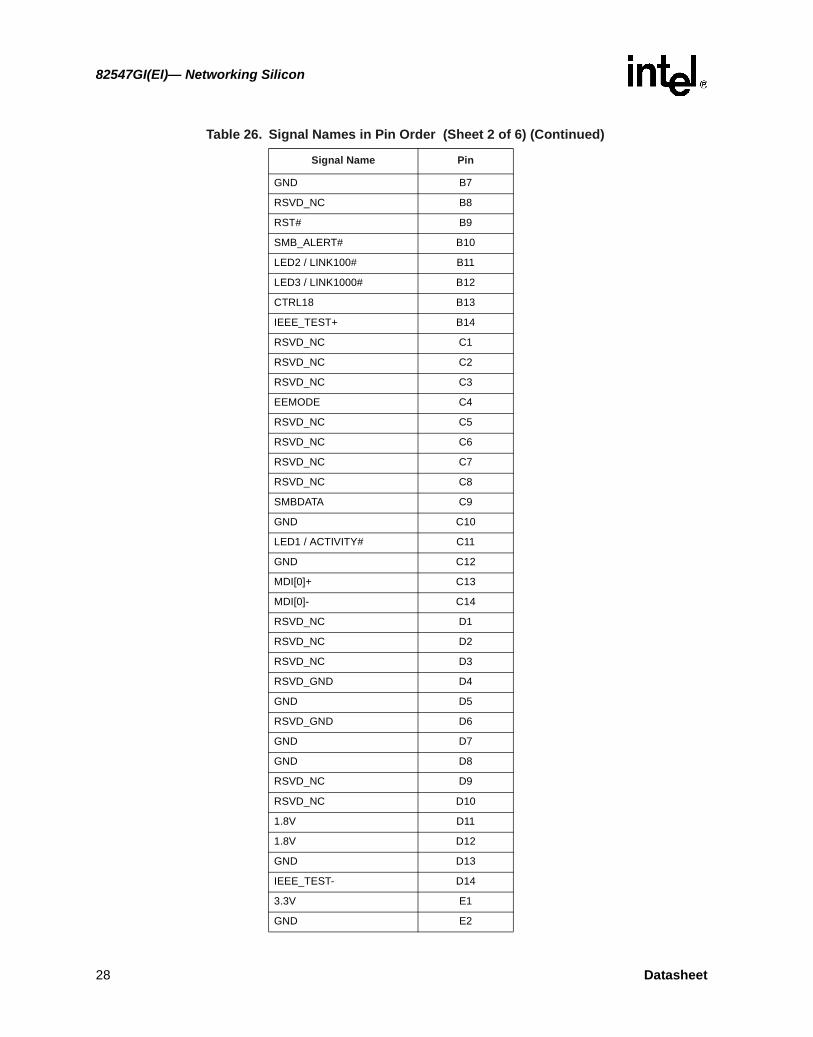
82547GI(EI)— Networking Silicon
GND B7
RSVD_NC B8
RST# B9
SMB_ALERT# B10
LED2 / LINK100# B11
LED3 / LINK1000# B12
CTRL18 B13
IEEE_TEST+ B14
RSVD_NC C1
RSVD_NC C2
RSVD_NC C3
EEMODE C4
RSVD_NC C5
RSVD_NC C6
RSVD_NC C7
RSVD_NC C8
SMBDATA C9
GND C10
LED1 / ACTIVITY# C11
GND C12
MDI[0]+ C13
MDI[0]- C14
RSVD_NC D1
RSVD_NC D2
RSVD_NC D3
RSVD_GND D4
GND D5
RSVD_GND D6
GND D7
GND D8
RSVD_NC D9
RSVD_NC D10
1.8V D11
1.8V D12
GND D13
IEEE_TEST- D14
3.3V E1
GND E2
Table 26. Signal Names in Pin Order (Sheet 2 of 6) (Continued)
Signal Name Pin
28 Datasheet

Networking Silicon —82547GI(EI)
RSVD_NC E3
RSVD_GND E4
GND E5
GND E6
GND E7
GND E8
GND E9
RSVD_GND E10
1.2V E11
1.2V E12
MDI[1]+ E13
MDI[1]- E14
RSVD_NC F1
RSVD_NC F2
RSVD_NC F3
GND F4
RSVD_GND F5
GND F6
GND F7
GND F8
GND F9
GND F10
GND F11
RSVD_NC F12
MDI[2]+ F13
MDI[2]- F14
CI_CLK G1
CI[9] G2
RSVD_NC G3
1.2V G4
1.2V G5
1.2V G6
GND G7
GND G8
GND G9
GND G10
GND G11
1.8V G12
Table 26. Signal Names in Pin Order (Sheet 3 of 6) (Continued)
Signal Name Pin
Datasheet 29

82547GI(EI)— Networking Silicon
1.2V G13
GND G14
CI[10] H1
GND H2
CI[8] H3
1.2V H4
1.2V H5
1.2V H6
1.2V H7
1.2V H8
GND H9
GND H10
1.2V H11
NC H12
MDI[3]+ H13
MDI[3]- H14
CI[0] J1
CI[1] J2
CI_2 J3
1.2V J4
1.2V J5
1.2V J6
1.2V J7
1.2V J8
1.2V J9
1.2V J10
1.2V J11
AUX_PWR J12
1.8V J13
XTAL2 J14
CI[3] K1
GND K2
3.3V K3
RSVD_3.3V K4
1.2V K5
1.2V K6
1.2V K7
1.2V K8
Table 26. Signal Names in Pin Order (Sheet 4 of 6) (Continued)
Signal Name Pin
30 Datasheet

Networking Silicon —82547GI(EI)
1.2V K9
1.2V K10
1.2V K11
GND K12
3.3V K13
XTAL1 K14
CI_STRS L1
CI_STRF L2
CI[4] L3
1.2V L4
1.2V L5
GND L6
RSVD_NC L7
RSVD_NC L8
1.2V L9
1.2V L10
GND L11
JTAG_TMS L12
JTAG_TRST# L13
JTAG_TCK L14
CI]6] M1
CI[5] M2
GND M3
1.2V M4
1.2V M5
GND M6
RSVD_NC M7
RSVD_NC M8
FLSH_CE# M9
EESK M10
FLSH_SI M11
SDP[3] M12
JTAG_TDI M13
JTAG_TDO M14
GND N1
CI[7] N2
CI_RCOMP N3
CI_VREF N4
Table 26. Signal Names in Pin Order (Sheet 5 of 6) (Continued)
Signal Name Pin
Datasheet 31
82547GI(EI)— Networking Silicon
1.2V N5
3.3V N6
RSVD_NC N7
3.3V N8
FLSH_SCK N9
EEDO N10
RSVD_NC N11
GND N12
SDP[2] N13
SDP[0] N14
NC P1
3.3V P2
CI_SWING P3
RSVD_NC P4
RSVD_NC P5
RSVD_NC P6
EECS P7
GND P8
FLSH_SO/LAN_DISABLE# P9
EEDI P10
CTRL12 P11
3.3V P12
SDP[1] P13
NC P14
Table 26. Signal Names in Pin Order (Sheet 6 of 6) (Continued)
Signal Name Pin
32 Datasheet

Networking Silicon —82547GI(EI)
5.4 Visual Pin Assignments
Figure 3. Visual Pin Assignments
3.3V CI_CLK NCVSSNC
VSS CI[9] 3.3VVSS
VSS 3.3V3.3V
EEMODE VSS VSS VSSCSA_1.2V 1.2V
1.2V3.3V
VSS VSS VSS 1.2V 1.2V 1.2V 1.2V1.2V
VSS VSS VSS 1.2V 1.2V 1.2V 3.3VVSSVSS1.2VPME#
VSS VSS VSS VSS VSS 1.2V 1.2V EECSNC1.2V3.3V
VSS VSS VSS VSS 1.2V 1.2V VSS3.3VNCNC1.2V
RST# SMBDATA NC VSS VSS VSS VSS 1.2V
FLSH_SO/LAN_DISABLE#
FLSH_SCK
FLSH_CE#
1.2V1.2VLAN_PWR_GOOD
SMB_ALERT
VSS NC VSS VSS VSS VSS 1.2V EEDIEEDOEESK1.2V1.2VSMBCLK
LED2/LINK100#
LED1/ACTIVITY# 1.8V
ANALOG_1.2V VSS VSS
ANALOG_1.2V 1.2V CTRL12NC
FLSH_
SIVSS1.2V3.3V
LED3/
LINK1000#
1.8VANALOG_
1.2V NC 1.8V NCAUX_PWR
3.3VVSSSDP[3]JTAG_
TMS
LED0/
LINK_UP#
CTRL18 MDI[0]+ MDI[1]+ MDI[2]+ANALOG_
1.2V MDI[3]+ 1.8V SDP[1]SDP[2]JTAG_
TDIJTAG_TRST#
3.3VTEST
IEEE_
TEST+MDI[0]-
IEEE_
TEST-MDI[1]- MDI[2]- MDI[3]- XTAL2 NCSDP[0]
JTAG_
TDO
JTAG_
TCKXTAL1NC
A B C D E F G H J K L M N P
1
2
3
4
5
6
7
8
9
10
11
12
13
14
NC
NC
NC
NC
NC
NC
NC
NC
NC
NC
NC
NC
NC
NC
NC
NC
NC
ANALOG_VSS
NC
NC
NC
ANALOG_VSS
NC
NC
NC
NC NC
ANALOG_VSS
CSA_
CI[8]
CSA_1.2V
CI[10] CI[0]
CI[1]
CI[2]
CSA_1.2V
CI[3]
CSA_
ANALOG_VSS
CI_STRS
CI_STRF
CI[4]
CI[6]
CI[5]
CSA_VSS
CSA_
1.2V
1.2V
NC
CSA_
CI[7]
CI_RCOMP
CI_VREF
1.2V
NC
CI_SWING
NC
NC
NC
Datasheet 33

82547GI(EI)— Networking Silicon
Note: This page is intentionally left blank.
34 Datasheet