8254 is a programmable interval timer. which with out...
TRANSCRIPT
8254 is a programmable interval timer. Which
is widely used in clock driven digital circuits.
with out timer there will not be proper
synchronization between two devices. So it is
very useful chip.
The 8254 consists of three independent
16-bit programmable counters (timers).
Each counter is capable of counting in binary or binary-
coded decimal (BCD).
◦ maximum allowable input frequency to any
counter is 10 MHz
Useful where the microprocessor must
control real-time events.
3
Usage includes real-time clocks, event counters, and
motor speed/direction control.
Timer appears in the PC decoded at ports 40H–43H to do
the following:
◦ 1. Generate a basic timer interrupt that occurs
at approximately 18.2 Hz
◦ 2. Cause the DRAM memory system to be refreshed
◦ 3. Provide a timing source to the internal
speaker and other devices.
4
• Timer in the PC is an 8253 instead of
8254.
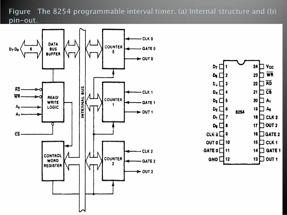
Figure shows the pin-out of the 8254,
a higher-speed version of the 8253, and a diagram of one
of the three counters.
Each timer contains:
◦ a CLK input which provides the basic operating
frequency to the timer
◦ a gate input pin which controls the timer in some modes
◦ an output (OUT) connection to obtain the output
of the timer
5
6
The signals that connect to the processor are the data bus
pins (D7–D0), RD, WR, CS, and address inputs A1 and A0.
Address inputs are present to select any of the four
internal registers.
◦ used for programming, reading, or writing to a counter
7
Timer zero generates an 18.2 Hz signal that interrupts the
microprocessor at interrupt vector 8 for a clock tick.
◦ often used to time programs and events in DOS
Timer 1 is programmed for 15 µs, used on
the PC to request a DMA action used to refresh the
dynamic RAM.
Timer 2 is programmed to generate a tone
on the PC speaker.
8
• The address inputs select one of four internal registers
within the 8254. See Table 11–4 for the function of the A1
and A0 address bits.
The clock input is the timing source for each of the
internal counters. This input is often connected to the
PCLK signal from the microprocessor system bus
controller.
9
CLK
A0, A1
Chip select enables 8254 for programming and reading or
writing a counter.
10
GATE
• The gate input controls the operation of the counter in
some modes of operation
GND
• Ground connects to the system ground bus.
A counter output is where the waveform generated by the
timer is available.
11
RD
• Read causes data to be read from the 8254 and often
connects to the IORC signal.
Vcc • Power connects to the +5.0 V power supply.
WR
• Write causes data to be written to the 8254 and often
connects to write strobe IOWC.
12
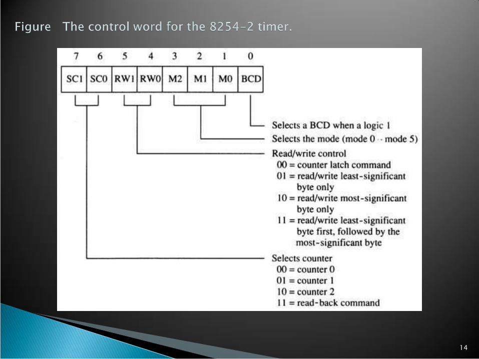
Each counter is programmed by writing a control word,
followed by the initial count.
◦ fig 11–34 lists the program control word structure
The control word allows the programmer to select the
counter, mode of operation, and type of operation
(read/write).
◦ also selects either a binary or BCD count
13
14
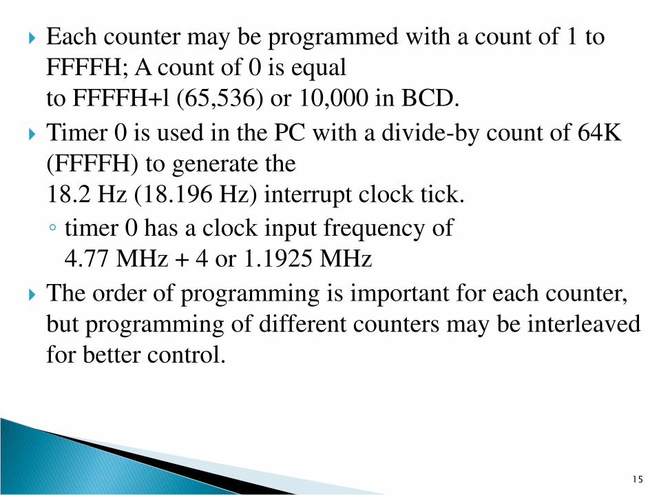
Each counter may be programmed with a count of 1 to
FFFFH; A count of 0 is equal
to FFFFH+l (65,536) or 10,000 in BCD.
Timer 0 is used in the PC with a divide-by count of 64K
(FFFFH) to generate the
18.2 Hz (18.196 Hz) interrupt clock tick.
◦ timer 0 has a clock input frequency of
4.77 MHz + 4 or 1.1925 MHz
The order of programming is important for each counter,
but programming of different counters may be interleaved
for better control.
15
16
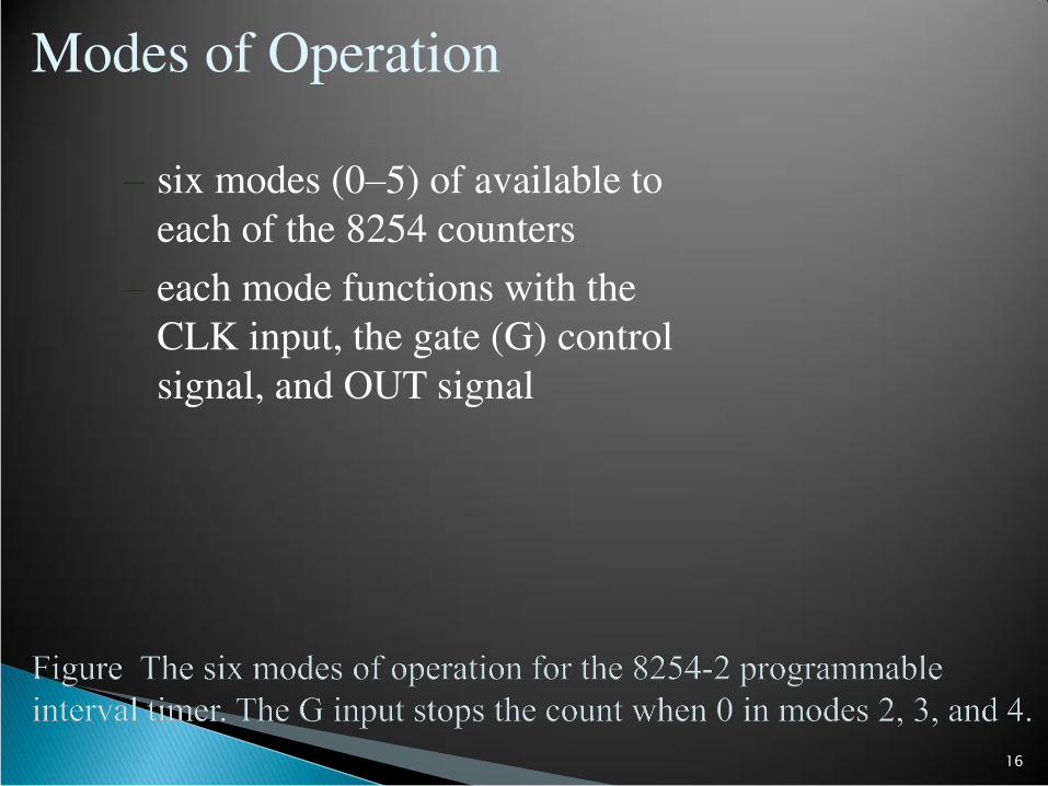
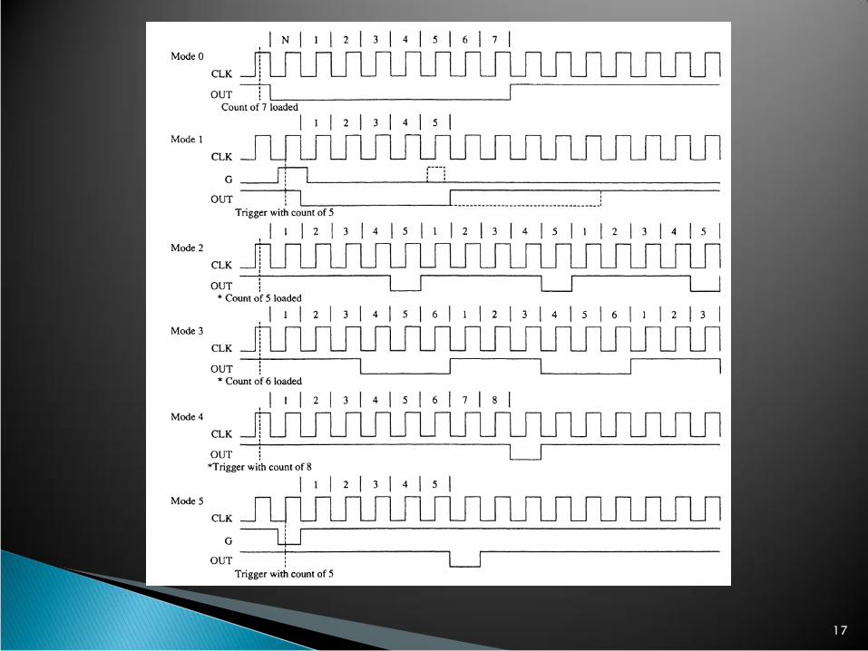
Modes of Operation
– six modes (0–5) of available to
each of the 8254 counters
– each mode functions with the
CLK input, the gate (G) control
signal, and OUT signal
17
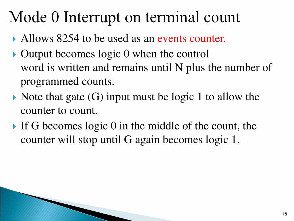
Allows 8254 to be used as an events counter.
Output becomes logic 0 when the control
word is written and remains until N plus the number of
programmed counts.
Note that gate (G) input must be logic 1 to allow the
counter to count.
If G becomes logic 0 in the middle of the count, the
counter will stop until G again becomes logic 1.
18
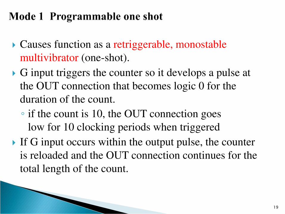
Causes function as a retriggerable, monostable
multivibrator (one-shot).
G input triggers the counter so it develops a pulse at
the OUT connection that becomes logic 0 for the
duration of the count.
◦ if the count is 10, the OUT connection goes
low for 10 clocking periods when triggered
If G input occurs within the output pulse, the counter
is reloaded and the OUT connection continues for the
total length of the count.
19
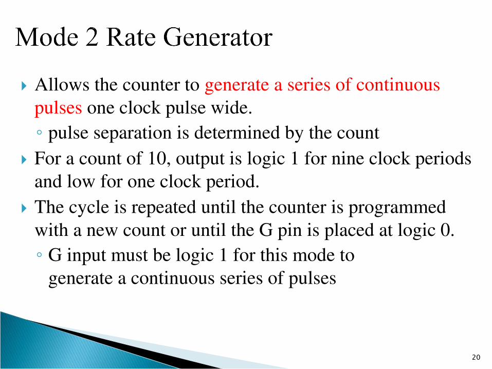
Allows the counter to generate a series of continuous
pulses one clock pulse wide.
◦ pulse separation is determined by the count
For a count of 10, output is logic 1 for nine clock periods
and low for one clock period.
The cycle is repeated until the counter is programmed
with a new count or until the G pin is placed at logic 0.
◦ G input must be logic 1 for this mode to
generate a continuous series of pulses
20
Generates a continuous square wave at the OUT
connection, provided the G pin is logic 1.
If the count is even, output is high for one half of the
count and low for one half of the count.
If the count is odd, output is high for one clocking
period longer than it is low.
◦ if the counter is programmed for a count of 5,
the output is high for three clocks and low for
two clocks
21
Allows a single pulse at the output.
If count is programmed as 10, output is high for 10 clocking periods and low for one period.
◦ the cycle does not begin until the counter is loaded with its complete count
Operates as a software triggered one-shot.
As with modes 2 and 3, this mode also uses the G input to enable the counter.
◦ G input must be logic 1 for the counter to operate for these three modes
22
A hardware triggered one-shot that functions as mode 4.
except it is started by a trigger pulse on the
G pin instead of by software
This mode is also similar to mode 1 because
it is retrigger able.
23
Scope of research in this field are design of
new timer chip which has more feature then
existing timer chip and which are capable to
interface with less hardware and software
supports.