8086 microprocessor architecture
TRANSCRIPT

Microprocessors and Microcontrollers
1
ByK. SAI KRISHNAAssistant Professor

Historical Background
2

3
• 1947- Invention of Transistor->Bell Laborites
• 1959- Invention of Integrated Circuit• 1965- Birth of Moore’s Law• 1971- Development of First
Microprocessor Developed by Intel
-> 4004 “cpu-on-a-chip”.• 1976- Introduction of Microcontroller
Developed by Intel
->8048 “computer-on-a-chip”.

Typical Features• Smaller Size• Lower Cost• Higher Reliability• Low Power Consumption• More Powerful• Higher Versatility.
4

Applications• General Purpose µp
-> Desktop, PCs, Laptops, Workstations, Servers.
• Microcontrollers: Embedded Systems
->Consumer Electronics: Toys, Cameras, Robots.
->Consumer Products: Washing Machines, Microwave Ovens.
5 Contd…

Applications->Instrumentation: Oscilloscopes, Medical Instruments.
-> Communications: Telephone Sets, Cordless Phones.
->Office: FAX Machines, Printers.
->Multimedia Applications: Cell Phones, Teleconferencing.
6

Brief Discussion
• What is Computer?
– CPU -> CU + ALU + registers– Memory -> RAM/ ROM– I/P AND O/P DEVICES
7

What is Microprocessor?
– 1960s’ CPU – designed with logic gates– LSI – Large Scale Integration– SSI to LSI – called Microprocessor– Microcomputer– Intel – 4 bit microprocessor 4004 in 1971– 8 bit microprocessor 8080– 8-bit 8085 (8 bit data bus + 16 bit address bus)– 16-bit 8086 (16 bit data bus + 20 bit address
bus)– 16 bit processors – 8088,80186,80188, 80286– 32 bit processors – 80386 , 80486, 80586 (P)
8

9
Microprocessors:
CPU
General-Purpose Micro-processor
RAM ROM I/O Port
TimerSerial COM Port
Data Bus
Address Bus
General-Purpose Microprocessor System
Many chips on mother’s board
General-purpose microprocessor• CPU for Computers• No RAM, ROM, I/O on CPU chip itself• Example: Intel’s x86, Motorola’s 680x0

What is Microcontroller?
• LSI to VLSI – called Microcontroller• To build Microprocessor, memory and I/O devices
on a single chip• Components
• Microprocessor• A/D Converter• D/A Converter• Parallel I/O Interface• Serial I/O Interface• Timers and Counters
10

11
Microcontroller :
• A smaller computer• On-chip RAM, ROM, I/O ports...• Example:Motorola’s 6811, Intel’s 8051, Zilog’s Z8
RAM ROM
I/O Port
TimerSerial COM Port
Microcontroller
CPU
A single chip

12
Microprocessor vs. Microcontroller
Microprocessor • CPU is stand-alone,
RAM, ROM, I/O, timer are separate
• designer can decide on the amount of ROM, RAM and I/O ports.
• expansive• versatility • general-purpose
Microcontroller• CPU, RAM, ROM, I/O and
timer are all on a single chip
• fix amount of on-chip ROM, RAM, I/O ports
• for applications in which cost, power and space are critical
• single-purpose

13
Microcontroller vs. Microprocessors

Refer History of Microprocessor pdf
14

Basic Concepts of MicroprocessorsDifferences between:
– Microcomputer – a computer with a microprocessor as its CPU. Includes memory, I/O etc.
– Microprocessor – silicon chip which includes ALU, register circuits & control circuits
– Microcontroller – silicon chip which includes microprocessor, memory & I/O in a single package.
15

What is a Microprocessor?• The word comes from the combination micro and
processor.
–Processor means a device that processes whatever. In this context processor means a device that processes numbers, specifically binary numbers, 0’s and 1’s.
To process means to manipulate. It is a general term that describes all manipulation. Again in this content, it means to perform certain operations on the numbers that depend on the microprocessor’s design.
16

What about micro?• Micro is a new addition.
–In the late 1960’s, processors were built using discrete elements. These devices performed the required operation, but were too large and too slow.
–In the early 1970’s the microchip was invented. All of the components that made up the processor were now placed on a single piece of silicon. The size became several thousand times smaller and the speed became several hundred times faster. The “Micro”Processor was born.
17

Definition of the Microprocessor
• The microprocessor is a programmable device that takes in numbers, performs on them arithmetic or logical operations according to the program stored in memory and then produces other numbers as a result.
18

Definition (Contd.)• Lets expand each of the underlined words:
–Programmable device: The microprocessor can perform different sets of operations on the data it receives depending on the sequence of instructions supplied in the given program.• By changing the program, the microprocessor
manipulates the data in different ways.
–Instructions: Each microprocessor is designed to execute a specific group of operations. This group of operations is called an instruction set. This instruction set defines what the microprocessor can and cannot do.19

Definition (Contd.)
– Takes in: The data that the microprocessor manipulates must come from somewhere.
• It comes from what is called “input devices”.
• These are devices that bring data into the system from the outside world.
• These represent devices such as a keyboard, a mouse, switches, and the like.
20

Definition (Contd.)–Numbers: The microprocessor has a very narrow view on life. It only understands binary numbers.
• A binary digit is called a bit (which comes from binary digit).
• The microprocessor recognizes and processes a group of bits together. This group of bits is called a “word”.
• The number of bits in a Microprocessor’s word, is a
measure of its “abilities”.21

Definition (Contd.)
• Words, Bytes, etc.
• The earliest microprocessor (the Intel 8088 and Motorola’s 6800) recognized 8-bit words.
– They processed information 8-bits at a time. That’s why they are called “8-bit processors”. They can handle large numbers, but in order to process these numbers, they broke them into 8-bit pieces and processed each group of 8-bits separately.
22

Definition (Contd.)
• Later microprocessors (8086 and 68000) were designed with 16-bit words.
– A group of 8-bits were referred to as a “half-word” or “byte”.
– A group of 4 bits is called a “nibble”.
– Also, 32 bit groups were given the name “long word”.
•Today, all processors manipulate at least 32 bits at a time and there exists microprocessors that can process 64, 80, 128 bits.
23

Definition (Contd.)– Arithmetic and Logic Operations:
•Every microprocessor has arithmetic operations such as add and subtract as part of its instruction set.
– Most microprocessors will have operations such as multiply and divide.
– Some of the newer ones will have complex operations such as square root.
• In addition, microprocessors have logic operations as well. Such as AND, OR, XOR, shift left, shift right, etc.
•Again, the number and types of operations define the microprocessor’s instruction set and depends on the specific microprocessor.
24

Definition (Contd.)– Stored in memory :
• First, what is memory?
– Memory is the location where information is kept while not in current use.
– Memory is a collection of storage devices. Usually, each storage device holds one bit. Also, in most kinds of memory, these storage devices are grouped into groups of 8. These 8 storage locations can only be accessed together. So, one can only read or write in terms of bytes to and form memory.
25

Definition (Contd.)– Stored in memory:
• When a program is entered into a computer, it is stored in memory. Then as the microprocessor starts to execute the instructions, it brings the instructions from memory one at a time.
• Memory is also used to hold the data.
– The microprocessor reads (brings in) the data from memory when it needs it and writes (stores) the results into memory when it is done.
26

Definition (Contd.)-Produces: For the user to see the result of the execution of the program, the results must be presented in a human readable form.
• The results must be presented on an output device.
• This can be the monitor, a paper from the printer, a
simple LED or many other forms.
27

A Microprocessor-based system• From the above description, we can draw the following
block diagram to represent a microprocessor-based system:
28

Inside The Microprocessor• Internally, the microprocessor is made up of 3
main units.
– The Arithmetic/Logic Unit (ALU)
– The Control Unit.
– An array of registers for holding data while it is being manipulated.
29

Organization of a microprocessor-based system
• Let’s expand the picture a bit.
30

Memory• Memory stores information such as instructions and data in
binary format (0 and 1). It provides this information to the microprocessor whenever it is needed.
• Usually, there is a memory “sub-system” in a microprocessor-based system. This sub-system includes:
– The registers inside the microprocessor
– Read Only Memory (ROM)
• used to store information that does not change.
– Random Access Memory (RAM) (also known as
Read/Write Memory).
•used to store information supplied by the user. Such as programs and data.
31Contd…

Memory Map and Addresses • The memory map is a picture representation of the address range and shows where the different memory chips are located within the address range
32
Contd…

Memory• To execute a program:
–the user enters its instructions in binary format into the memory.
–The microprocessor then reads these instructions and whatever data is needed from memory, executes the instructions and places the results either in memory or produces it on an output device.
33

The three cycle instruction execution model
• To execute a program, the microprocessor “reads” each instruction from memory, “interprets” it, then “executes” it.
• To use the right names for the cycles:
– The microprocessor fetches each instruction,
– decodes it,
– Then executes it.
•This sequence is continued until all instructions are performed.
34

Machine Language• The number of bits that form the “word” of a microprocessor
is fixed for that particular processor.
– These bits define a maximum number of combinations.
•For example an 8-bit microprocessor can have at most 28 = 256 different combinations.
•However, in most microprocessors, not all of these combinations are used.
– Certain patterns are chosen and assigned specific meanings.
– Each of these patterns forms an instruction for the microprocessor.
– The complete set of patterns makes up the microprocessor’s machine language.
35

The 8085 Machine Language• The 8085 (from Intel) is an 8-bit microprocessor.
–The 8085 uses a total of 246 bit patterns to form its instruction set.
– These 246 patterns represent only 74 instructions.
• The reason for the difference is that some (actually most)
instructions have multiple different formats.
–Because it is very difficult to enter the bit patterns correctly, they are usually entered in hexadecimal instead of binary.
•For example, the combination 0011 1100 indicated in hexa decimal is 3C.
36

Assembly Language• Entering the instructions using hexadecimal is quite
easier than entering the binary combinations.
–However, it still is difficult to understand what a program written in hexadecimal does.
–So, each company defines a symbolic code for the instructions.
– These codes are called “mnemonics”.
–The mnemonic for each instruction is usually a group of letters that suggest the operation performed.
37Contd…

Assembly Language• Using the same example from before,
– 00111100 translates to 3C in hexadecimal (OPCODE)
– Its mnemonic is: “INR A”.
–INR stands for “increment register” and A is short for accumulator.
• Another example is: 1000 0000,
– Which translates to 80 in hexadecimal.
– Its mnemonic is “ADD B”.
–“Add register B to the accumulator and keep the result in the accumulator”.
38Contd…

Assembly Language• It is important to remember that a machine language and its
associated assembly language are completely machine dependent.
–In other words, they are not transferable from one microprocessor to a different one.
•For example, Motorola has an 8-bit microprocessor called the 6800.
–The 8085 machine language is very different from that of the 6800.
–A program written for the 8085 cannot be executed on the 6800 and vice versa.
39Contd…

“Assembling” The Program• How does assembly language get translated into
machine language?
– There are two ways:
– 1st there is “hand assembly”.
•The programmer translates each assembly language instruction into its equivalent hexadecimal code (machine language). Then the hexadecimal code is entered into memory.
– The other possibility is a program called an
“assembler”, which does the translation automatically.40

8085 Microprocessor Architecture
• 8-bit general purpose µp
• Capable of addressing 64 k of memory
• Has 40 pins
• Requires +5 v power supply
• Can operate with 3 MHz clock
41

42

43

• System Bus – wires connecting memory & I/O to
microprocessor
– Address Bus
• Unidirectional
• Identifying peripheral or memory location
– Data Bus
• Bidirectional
• Transferring data
– Control Bus
• Synchronization signals
• Timing signals
• Control signal44

45

Intel 8085 Microprocessor
• Microprocessor consists of:
– Control unit: control microprocessor operations.
– ALU: performs data processing function.
– Registers: provide storage internal to CPU.
– Interrupts
– Internal data bus
46

The ALU
• In addition to the arithmetic & logic circuits, the ALU includes the accumulator, which is part of every arithmetic & logic operation.
• Also, the ALU includes a temporary register used for holding data temporarily during the execution of the operation. This temporary register is not accessible by the programmer.
47

48

49

The Salient Features of 8085 Microprocessor:
• It is an 8 bit processor.
• It is a single chip N-MOS device with 40 pins.
• It has multiplexed address and data bus.(AD0-AD7).
• It works on 5 Volt dc power supply.
• The maximum clock frequency is 3 MHz while minimum frequency is 500kHz.
• It provides 74 instructions with 5 different addressing modes.
50Contd….

The Salient Features of 8085 Microprocessor:
• It provides 16 address lines so it can access 2^16 =64K bytes of memory.
• It generates 8 bit I/O address so it can access 2^8=256 input ports.
• It provides 5 hardware interrupts:TRAP, RST 5.5, RST 6.5, RST 7.5,INTR.
• It provides Acc ,one flag register ,6 general purpose registers and two special purpose registers(SP,PC).
• It provides serial lines SID ,SOD.So serial peripherals can be interfaced with 8085 directly.
51

52
Introduction to 8086

Intel 8086MICROPROCESSORIntel 8086MICROPROCESSOR
53

Features Features
It is a 16-bit μp.
8086 has a 20 bit address bus can access up to 220 memory locations (1 MB).
It can support up to 64K I/O ports.
It provides 14, 16 -bit registers.
Word size is 16 bits.
It has multiplexed address and data bus AD0- AD15 and A16 – A19.
It requires single phase clock with 33% duty cycle to provide internal timing.
54

8086 is designed to operate in two modes, Minimum and Maximum.
It can prefetches up to 6 instruction bytes from memory and queues them in order to speed up instruction execution.
It requires +5V power supply.
A 40 pin dual in line package.
Address ranges from 00000H to FFFFFH
Memory is byte addressable - Every byte has a separate address.
55

Intel 8086 Internal ArchitectureIntel 8086 Internal Architecture
56

Internal architecture of 8086Internal architecture of 8086
• 8086 has two blocks BIU and EU.
• The BIU handles all transactions of data and addresses on the buses for EU.
• The BIU performs all bus operations such as instruction fetching, reading and writing operands for memory and calculating the addresses of the memory operands. The instruction bytes are transferred to the instruction queue.
• EU executes instructions from the instruction system byte queue.
57

• Both units operate asynchronously to give the 8086 an overlapping instruction fetch and execution mechanism which is called as Pipelining. This results in efficient use of the system bus and system performance.
• BIU contains Instruction queue, Segment registers, Instruction pointer, Address adder.
• EU contains Control circuitry, Instruction decoder, ALU, Pointer and Index register, Flag register.
58

EXECUTION UNITEXECUTION UNIT
• Decodes instructions fetched by the BIU• Generate control signals,• Executes instructions.
The main parts are:
• Control Circuitry• Instruction decoder• ALU
59

EXECUTION UNIT – General Purpose RegistersEXECUTION UNIT – General Purpose Registers
AH AL
BH BL
CH CL
DH DL
SP
BP
SI
DI
60
8 bits 8 bits
16 bits
Accumulator
Base
Count
Data
Stack Pointer
Base Pointer
Source Index
Destination Index
AX
BX
CX
DX
Pointer
Index
8 bits 8 bits
16 bits
Accumulator
Base
Count
Data
Stack Pointer
Base Pointer
Source Index
Destination Index

EXECUTION UNIT – General Purpose RegistersEXECUTION UNIT – General Purpose Registers
Register PurposeAX Word multiply, word divide, word I /O
AL Byte multiply, byte divide, byte I/O, decimal arithmetic
AH Byte multiply, byte divide
BX Store address information
CX String operation, loops
CL Variable shift and rotate
DX Word multiply, word divide, indirect I/O(Used to hold I/O address during I/O instructions. If the result is more than 16-bits, the lower order 16-bits are stored in accumulator and higher order 16-bits are stored in DX register) 61

Pointer And Index RegistersPointer And Index Registers• used to keep offset addresses.
• Used in various forms of memory addressing.
• In the case of SP and BP the default reference to form a physical address is the Stack Segment (SS-will be discussed under the BIU)
• The index registers (SI & DI) and the BX generally default to the Data segment register (DS).
SP: Stack pointer– Used with SS to access the stack segment
BP: Base Pointer– Primarily used to access data on the stack– Can be used to access data in other segments
62

• SI: Source Index register– is required for some string operations– When string operations are performed, the SI register points to memory locations in the data segment which is addressed by the DS register. Thus, SI is associated with the DS in string operations.
• DI: Destination Index register– is also required for some string operations.– When string operations are performed, the DI register points to memory locations in the data segment which is addressed by the ES register. Thus, DI is associated with the ES in string operations.
• The SI and the DI registers may also be used to access data stored in arrays
63
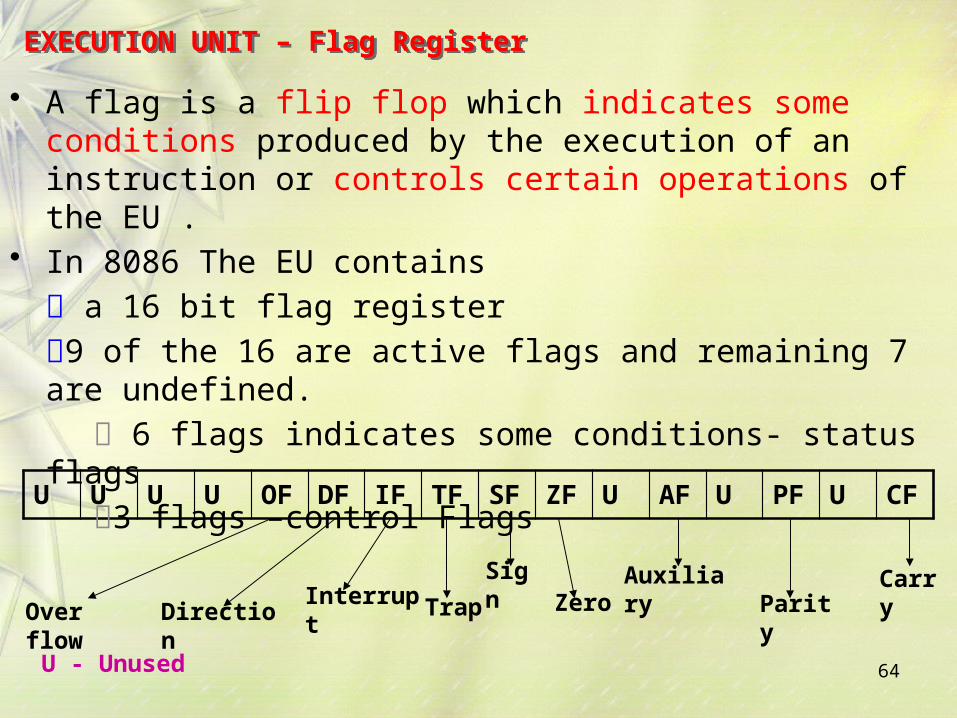
EXECUTION UNIT – Flag RegisterEXECUTION UNIT – Flag Register
U U U U OF
DF
IF TF
SF
ZF
U AF
U PF
U CF
64
• A flag is a flip flop which indicates some conditions produced by the execution of an instruction or controls certain operations of the EU .
• In 8086 The EU contains
a 16 bit flag register
9 of the 16 are active flags and remaining 7 are undefined.
6 flags indicates some conditions- status flags
3 flags –control Flags
Carry Over flow Direction
Interrupt Trap
SignZero
AuxiliaryParity
U - Unused

EXECUTION UNIT – Flag RegisterEXECUTION UNIT – Flag Register
Flag Purpose
Carry (CF) Holds the carry after addition or the borrow after subtraction.Also indicates some error conditions, as dictated by some programs and procedures .
Parity (PF) PF=0;odd parity, PF=1;even parity.
Auxiliary (AF) Holds the carry (half – carry) after addition or borrow aftersubtraction between bit positions 3 and 4 of the result (for example, in BCD addition or subtraction.)
Zero (ZF) Shows the result of the arithmetic or logic operation.Z=1; result is zero. Z=0; The result is 0
Sign (SF) Holds the sign of the result after an arithmetic/logic instructionexecution. S=1; negative, S=0 65

Flag Purpose
Trap (TF)A control flag.Enables the trapping through an on-chip debugging feature.
Interrupt (IF)A control flag.Controls the operation of the INTR (interrupt request)I=0; INTR pin disabled. I=1; INTR pin enabled.
Direction (DF)A control flag.It selects either the increment or decrement mode for DI and /or SI registers during the string instructions.
Overflow (OF)Overflow occurs when signed numbers are added or subtracted. An overflow indicates the result has exceeded the capacity of the Machine
66

Execution unit – Flag RegisterExecution unit – Flag Register
• Six of the flags are status indicators reflecting properties of the last arithmetic or logical instruction.
• For example, if register AL = 7Fh and the instruction ADD AL,1 is executed then the following happen
AL = 80hCF = 0; there is no carry out of bit 7PF = 0; 80h has an odd number of onesAF = 1; there is a carry out of bit 3 into bit 4ZF = 0; the result is not zeroSF = 1; bit seven is oneOF = 1; the sign bit has changed
67

BUS INTERFACE UNIT (BIU)BUS INTERFACE UNIT (BIU)Contains• 6-byte Instruction Queue (Q)• The Segment Registers (CS, DS, ES, SS).• The Instruction Pointer (IP).• The Address Summing block (Σ)
68

THE QUEUE (Q)THE QUEUE (Q)
• The BIU uses a mechanism known as an instruction stream queue to implement a pipeline architecture.
• This queue permits pre-fetch of up to 6 bytes of instruction code. Whenever the queue of the BIU is not full, it has room for at least two more bytes and at the same time the EU is not requesting it to read or write operands from memory, the BIU is free to look ahead in the program by pre-fetching the next sequential instruction.
69

• These pre-fetching instructions are held in its FIFO queue. With its 16 bit data bus, the BIU fetches two instruction bytes in a single memory cycle.
• After a byte is loaded at the input end of the queue, it automatically shifts up through the FIFO to the empty location nearest the output.
• The EU accesses the queue from the output end. It reads one instruction byte after the other from the output of the queue.
• The intervals of no bus activity, which may occur between bus cycles are known as Idle state.
70

Segmented MemorySegmented Memory
Code segment (64KB)
Data segment (64KB)
Extra segment (64KB)
Stack segment (64KB)
71
1 MB
The memory in an 8086/88 based system is organized as segmented memory.
The CPU 8086 is able to address 1Mbyte of memory.
The Complete physically available memory may be divided into a number of logical segments.
00000
FFFFF
Physical Memory

• The size of each segment is 64 KB• A segment is an area that begins at any location which is
divisible by 16.• A segment may be located any where in the memory• Each of these segments can be used for a specific
function.
– Code segment is used for storing the instructions.– The stack segment is used as a stack and it is used to store the
return addresses.– The data and extra segments are used for storing data byte.
* In the assembly language programming, more than one data/ code/ stack segments can be defined. But only one segment of each type can be accessed at any time.
72

• The 4 segments are Code, Data, Extra and Stack segments.• A Segment is a 64kbyte block of memory.• The 16 bit contents of the segment registers in the BIU
actually point to the starting location of a particular segment.• Segments may be overlapped or non-overlapped
Advantages of Segmented memory Scheme• Allows the memory capacity to be 1Mb although the actual addresses to
be handled are of 16 bit size.• Allows the placing of code, data and stack portions of the same program
in different parts (segments) of the m/y, for data and code protection.• Permits a program and/or its data to be put into different areas of
memory each time program is executed, i.e. provision for relocation may be done .
• The segment registers are used to allow the instruction, data or stack portion of a program to be more than 64Kbytes long. The above can be achieved by using more than one code, data or stack segments.
73

Segment registersSegment registers
• In 8086/88 the processors have 4 segments registers
• Code Segment register (CS), Data Segment register (DS), Extra Segment register (ES) and Stack Segment (SS) register.
• All are 16 bit registers.
• Each of the Segment registers store the upper 16 bit address of the starting address of the corresponding segments.
74

75

34BA
44EB
54EB
695E
76
CSR
DSR
ESR
SSR
Segment Registers
BIU
CODE (64k)
DATA (64K)
EXTRA (64K)
STACK (64K)
1 MB
00000
34BA0
44B9F
44EB0
54EAF
54EB0
64EAF
695E0
795DF
Each segment register store the upper 16 bit of the starting address of the segments
MEMORY

Instruction pointer & summing blockInstruction pointer & summing block
• The instruction pointer register contains a 16-bit offset address of instruction that is to be executed next.
• The IP always references the Code segment register (CS).
• The value contained in the instruction pointer is called as an offset because this value must be added to the base address of the code segment, which is available in the CS register to find the 20-bit physical address.
• The value of the instruction pointer is incremented after executing every instruction.
• To form a 20bit address of the next instruction, the 16 bit address of the IP is added (by the address summing block) to the address contained in the CS , which has been shifted four bits to the left.
77

78

• The following examples shows the CS:IP scheme of address formation:
79
Inserting a hexadecimal 0H (0000B)
with the CSR or shifting the CSR
four binary digits left
3 4 B A 0 ( C S ) +8 A B 4 ( I P )
3 D 6 5 4 (next address)
34BA 8AB4CS IP
34BA0
3D645
44B9F
Code segment
8AB4 (offset)

• Example For Address Calculation (segment: offset)
• If the data segment starts at location 1000h and a data reference contains the address 29h where is the actual data?
80
Required Address
Offset
Segment Address
0000 0000 0010 1001
0000
0001 0000 0000 0010 1001
0001 0000 0000 0000

Segment and Address register combinationSegment and Address register combination
• CS:IP
• SS:SP SS:BP
• DS:BX DS:SI
• DS:DI (for other than string operations)
• ES:DI (for string operations)
81

Summary of Registers & Pipeline of 8086 µPSummary of Registers & Pipeline of 8086 µP
AH AL
BH BL
CH CL
DH DL
82
SP
BP
SI
DI
FLAGS
DECODER
ALU
AX
BX
CX
DX
EU
Timing control
SP
BP
Default Assignment
BIU
IP
CS DS ES SS
PIPELINE(or)
QUEUE
CODE OUT
CODE IN
IP BX
DI
SI
DI
Fetch & store code bytes in PIPELINE

General Bus Operation
83

• The 8086 has a combined address and data bus commonly referred as a time multiplexed address and data bus.
• The main reason behind multiplexing address and data over the same pins is the maximum utilization of processor pins and it facilitates the use of 40 pin standard DIP package.
• The bus can be demultiplexed using a few latches and transceivers, when ever required.
84
General Bus Operation- Description

General Bus Operation (Contd…)
• Basically, all the processor bus cycles consist of at least four clock cycles. These are referred to as T1, T2, T3, and T4. The address is transmitted by the processor during T1. It is present on the bus only for one cycle.
• The negative edge of this ALE pulse is used to separate the address and the data or status information. In maximum mode, the status lines S0, S1 and S2 are used to indicate the type of operation.
• Status bits S3 to S7 are multiplexed with higher order address bits and the BHE signal. Address is valid during T1 while status bits S3 to S7 are valid during T2 through T4.
85
86

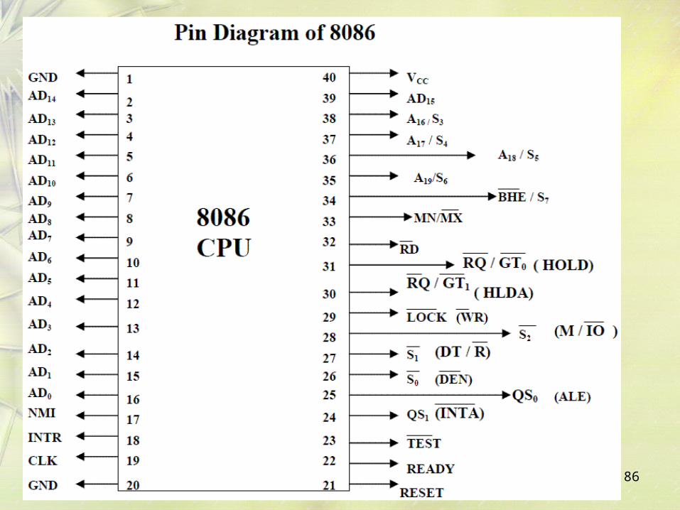
Pin Description of 8086
87
• The Microprocessor 8086 is a 16-bit CPU available in different clock rates and packaged in a 40 pin plastic package.
• The 8086 operates in single processor or multiprocessor configuration to achieve high performance. The pins serve a particular function in minimum mode (single processor mode) and other function in maximum mode configuration (multiprocessor mode).

Pin Description of 8086 (Contd…)
• The 8086 signals can be categorized in three groups. – The first are the signal having common
functions in minimum as well as maximum mode.
– The second are the signals which have special functions for minimum mode
– The third are the signals having special functions for maximum mode.
88

89

Pin Description of 8086 (Contd…)
90
Vcc (pin 40) : Power
Gnd (pin 1 and 20) : Ground
AD0..AD7 , AD8..AD15 , A19/S6, A18/S5, A17/S4, A16/S3 : 20 -bit Address Bus
MN/MX’ (input) : Indicates Operating mode
READY (input , Active High) : take µP to wait state
CLK (input) : Provides basic timing for the processor
RESET (input, Active High) : At least 4 clock cycles Causes the µP immediately terminate its present activity.
TEST’ (input , Active Low) : Connect this to HIGH
HOLD (input , Active High) : Connect this to LOW (BR)
HLDA (output , Active High) : Hold Ack (BG)
INTR (input , Active High) : Interrupt request
INTA’ (output , Active Low) : Interrupt AcknowledgeNMI (input , Active High) : Non-maskable interrupt

Pin Description of 8086 (Contd…)
91
DEN’ (output) : Data Enable. It is LOW when processor wants to receive data or processor is giving out data
DT/R’ (output) : Data Transmit/Receive. When High, data from µP to memory
When Low, data is from memory to µP
IO/M’ (output) : If High µP access I/O Device. If Low µP access memory
RD’ (output) : When Low, µP is performing a read operation
WR’ (output) : When Low, µP is performing a write operation
ALE (output) : Address Latch Enable , Active High Provided by µP to latch address When HIGH, µP is using AD0..AD7, A19/S6, A18/S5, A17/S4, A16/S3 as address lines

Pin Description of 8086 in Detail
92
Power Connections
1
19
20
40GND
CLK
GND
VCC
8086
Pin Description:GND – Pin no. 1, 20GroundCLK – Pin no. 19 – Type IClock: provides the basic timing for the processor and bus controller. It is asymmetric with a 33% duty cycle to provide optimized internal timing.VCC – Pin no. 40VCC: +5V power supply pin
Contd…..

93
Address/ Data Lines
10
11
12
13
14
15
16
39AD14
AD13
AD12
AD11
AD10
AD9
AD8
AD7
AD6
AD5
AD4
AD3
AD2
AD1
AD0
8086
2
3
4
5
6
7
8
9
AD15
Contd…..

94
Pin Description
AD15-AD0 – Pin no. 2-16, 39 – Type I/O
Address Data bus: These lines constitute the time multiplexed memory/ IO address (T1) and data (T2, T3, TW, T4) bus. A0 is
analogous to BHE* for the lower byte of the data bus, pins D7-D0. It is low when a byte is to be transferred on the lower portion of the bus in memory or I/O operations. Eight –bit oriented devices tied to the lower half would normally use A0 to condition chip select functions. These lines are active HIGH
Contd…..

95
Address Lines
8086
35
36
37
38 16A
17A
18A
19A
A14
A13
A12
A11
A10
A9
A8
A7
A6
A5
A4
A3
A2
A1
A0
A1539
10
11
12
13
14
15
16
2
3
4
5
6
7
8
9
Contd…..

96
Description:A19/S6, A18/S5, A17/S4, A16/S3 – Pin no. 35-38 – Type O
Address / Status: During T1 these are the four most significant address lines for memory operations. During I/O operations these lines are low. During memory and I/O operations, status information is available on these lines during T2, T3, TW and T4. The status of the interrupt enable FLAG bit (S5) is updated at the beginning of each CLK cycle. A17/S4 and A16/S3 are encoded as shown. A17/S4 A16/S3 Characteristic
s
0 (LOW) 0 Alternate Data
0 1 Stack
1(HIGH) 0 Code or None
1 1 Data
S6 is 0 (LOW)
This information indicates which relocation register is presently being used for data accessing.
Contd…..

97
Status Pins S0-S7
26
27
28
34
35
36
37
38
8086
0S )( DEN
1S )R(DT/
2S )O(M/I
S7
S6
S5
S4
S3
Pin Description:
Status: active during T4, T1 and T2
and is returned to the passive
state (1,1,1) during T3 or during
TW when READY is HIGH. This
status is used by the 8288 Bus
Controller to generate all memory
and I/O access control signals.
Any change by , or during T4 is
2S , 1S , 0S - Pin no. 26, 27, 28 – Type O
used to indicate the beginning of a bus cycle and the return to
the passive state in T3 or TW is used to indicate the end of a
bus cycle.Contd…..

98
Status DetailsIndication
0 0 0 Interrupt Acknowledge
0 0 1 Read I/O port
0 1 0 Write I/O port
0 1 1 Halt
1 0 0 Code access
1 0 1 Read memory
1 1 0 Write memory
1 1 1 Passive
Contd…..
2S 1S 0S

99
S4 S3 Indications
0 0 Alternate data0 1 Stack1 0 Code or none1 1 Data 5S -- Value of
Interrupt Enable flag
----- Always low (logical) indicating 8086 is on the bus. If it is tristated another bus master has taken control of the system bus.
6S
----- Used by 8087 numeric coprocessor to determine whether the CPU is a 8086 or 8088
7SContd…..

100
Interrupts
17
18
8086
NMI
INTR
Pin Description:NMI – Pin no. 17 – Type INon – Maskable Interrupt: an edge triggered input which causes a type 2 interrupt. A subroutine is vectored to via an interrupt vector lookup table located in system memory. NMI is not maskable internally by software. A transition from a LOW to HIGH initiates the interrupt at the end of the current instruction. This input is internally synchronized.
Contd…..
101
INTR – Pin No. 18 – Type IInterrupt Request: is a level triggered input which is sampled during the last clock cycle of each instruction to determine if the processor should enter into an interrupt acknowledge operation. A subroutine is vectored to via an interrupt vector lookup table located in system memory. It can be internally masked by software resetting the interrupt enable bit. INTR is internally synchronized. This signal is active HIGH.
Contd…..

102
Min mode signals
8086
DEN
RDT/
OM/I
HLDA
HOLD
WR
ALE
INTA
VCC
26
27
28
24
25
29
30
31
33 MXMN/
Contd…..

103
Pin Description
HOLD, HLDA – Pin no. 31, 30 – Type I/OHOLD: indicates that another master is requesting a local bus “hold”. To be acknowledged, HOLD must be active HIGH. The processor receiving the “hold” request will issue HLDA (HIGH) as an acknowledgement in the middle of a T1 clock cycle. Simultaneous with the issuance of HLDA the processor will float the local bus and control lines. After HOLD is detected as being LOW, the processor will LOWer the HLDA, and when the processor needs to run another cycle, it will again drive the local bus and control lines.The same rules as apply regarding when the local bus will be released.HOLD is not an asynchronous input. External synchronization should be provided if the system can not otherwise guarantee the setup time.
Contd…..

104
WR* - Pin no. 29 – Type OWrite: indicates that the processor is performing a write memory or write I/O cycle, depending on the state of the M/IO* signal. WR* is active for T2, T3 and TW of any write cycle. It is active LOW, and floats to 3-state OFF in local bus “hold acknowledge”.
M/IO* - Pin no. 28 – type OStatus line: logically equivalent to S2 in the maximum mode. It is used to distinguish a memory access from an I/O access. M/IO* becomes valid in the T4 preceding a bus cycle and remains valid until the final T4 of the cycle (M=HIGH), IO=LOW). M/IO* floats to 3-state OFF in local bus “hold acknowledge”.
Contd…..

105
DT/R* - Pin no. 27 – Type OData Transmit / Receive: needed in minimum system that desires to use an 8286/8287 data bus transceiver. It is used to control the direction of data flow through the transceiver. Logically DT/R* is equivalent to S1* in the maximum mode, and its timing is the same as for M/IO*. (T=HIGH, R=LOW). This signal floats to 3-state OFF in local bus “hold acknowledge”.
DEN* - Pin no. 26 – Type O Data Enable: provided as an output enable for the 8286/8287 in a minimum system which uses the transceiver. DEN* is active LOW during each memory and I/O access and for INTA cycles. For a read or INTA* cycle it is active from the middle of T2 until the middle of T4, while for a write cycle it is active from the beginning of T2 until the middle of T4. DEN* floats to 3-state OFF in local bus “hold acknowledge”.
Contd…..

106
ALE – Pin no. 25 – Type O Address Latch Enable: provided by the processor to latch the address into the 8282/8283 address latch. It is a HIGH pulse active during T1 of any bus cycle. Note that ALE is never floated.
INTA* - Pin no. 24 – Type OINTA* is used as a read strobe for interrupt acknowledge cycles. It is active LOW during T2, T3 and TW of each interrupt acknowledge cycle.
Contd…..

107
Max mode signals
8086
GND
26
27
28
24
25
29
30
31
33
0GT/RQ
1GT/RQ
LOCK
2S
1S
0S
QS0
QS1
Pin Description:
RQ*/GT0*, RQ*/GT1* - Pin no. 30, 31 – Type I/O
Request /Grant: pins are used by other local bus masters to force the processor to release the local bus at the end of the processor’s current bus cycle. Each pin is bidirectional with RQ*/GT0* having higher priority than RQ*/GT1*. RQ*/GT* has an internal pull up resistor so may be left unconnected. The request/grant sequence is as follows:
Contd…..

108
1. A pulse of 1 CLK wide from another local bus master indicates a local bus request (“hold”) to the 8086 (pulse 1)
2. During a T4 or T1 clock cycle, a pulse 1 CLK wide from the 8086 to the requesting master (pulse 2), indicates that the 8086 has allowed the local bus to float and that it will enter the “hold acknowledge” state at the next CLK. The CPU’s bus interface unit is disconnected logically from the local bus during “hold acknowledge”.
3. A pulse 1 CLK wide from the requesting master indicates to the 8086 (pulse 3) that the “hold” request is about to end and that the 8086 can reclaim the local bus at the next CLK.
Contd…..

109
Each master-master exchange of the local bus is a sequence of 3 pulses. There must be one dead CLK cycle after each bus exchange. Pulses are active LOW.If the request is made while the CPU is performing a memory cycle, it will release the local bus during T4 of the cycle when all the following conditions are met: Request occurs on or before T2. Current cycle is not the low byte of a word (on an odd address) Current cycle is not the first acknowledge of an interrupt acknowledge sequence. A locked instruction is not currently executing.
Contd…..

110
LOCK* - Pin no. 29 – Type O
LOCK* : output indicates that other system bus masters are not to gain control of the system bus while LOCK* is active LOW. The LOCK* signal is activated by the “LOCK” prefix instruction and remains active until the completion of the next instruction. This signal is active LOW, and floats to 3-state OFF in “hold acknowledge”.
QS1, QS0 – Pin no. 24, 25 – Type O
Queue Status: the queue status is valid during the CLK cycle after which the queue operation is performed.
QS1 and QS0 provide status to allow external tracking of the internal 8086 instruction queue.
Contd…..

111
QS1 QS0 Characteristics
0(LOW) 0 No operation
0 1 First Byte of Op Code from Queue
1 (HIGH) 0 Empty the Queue
1 1 Subsequent byte from Queue
Contd…..

112Contd…..
Common Signals

113Contd…..
Pin Description:
RD* - Pin no. 34, Type ORead: Read strobe indicates that the processor is performing a memory of I/O read cycle, depending on the state of the S2 pin. This signal is used to read devices which reside on the 8086 local bus. RD* is active LOW during T2, T3 and TW of any read cycle, and is guaranteed to remain HIGH in T2 until the 8086 local bus has floated.This signal floats to 3-state OFF in “hold acknowledge”.
READY – Pin no. 22, Type IREADY: is the acknowledgement from the addressed memory or I/O device that it will complete the data transfer. The READY signal from memory / IO is synchronized by the 8284A Clock Generator to form READY. This signal is active HIGH. The 8086 READY input is not synchronized. Correct operation is not guaranteed if the setup and hold times are not met.

114Contd…..
TEST* - Pin No 23 – Type ITEST* : input is examined by the “Wait” instruction. If the TEST* input is LOW execution continues, otherwise the processor waits in an “idle” state. This input is synchronized internally during each clock cycle on the leading edge of CLK.
RESET – Pin no. 21 – Type IReset: causes the processor to immediately terminate its present activity. The signal must be active HIGH for at least four clock cycles. It restarts execution, as described in the instruction set description, when RESET returns LOW. RESET is internally synchronized.

115Contd…..
BHE*/S7- Pin No. 34 – Type OBus High Enable / Status: During T1 the Bus High Enable signal (BHE*) should be used to enable data onto the most significant half of the data bus, pins D15-D8. Eight bit oriented devices tied to the upper half of the bus would normally use BHE* to condition chip select functions. BHE* is LOW during T1 for read, write, and interrupt acknowledge cycles when a byte is to be transferred on the high portion of the bus. The S7 status information is available during T2, T3 and T4. The signal is active LOW and floats to 3-state OFF in “hold”. It is LOW during T1 for the first interrupt acknowledge cycle.
BHE* A0 Characteristics
0 0 Whole word
0 1 Upper byte from / to odd address
1 0 Lower byte from / to even address
1 1 None

116Contd…..
MN/MX* - Pin no. 33 – Type - IMinimum / Maximum: indicates what mode the processor is to operate in.
If the local bus is idle when the request is made the two possible events will follow: Local bus will be released during the next clock. A memory cycle will start within 3 clocks. Now the four rules
for a currently active memory cycle apply with condition number 1 already satisfied.

117
Minimum Mode 8086 System

118Contd…..
A minimum mode of 8086 configuration depicts a stand alone system of computer where no other processor is connected. This is similar to 8085 block diagram with the following difference. The Data transceiver block which helps the signals traveling a longer distance to get boosted up. Two control signals data transmit/ receive are connected to the direction input of transceiver (Transmitter/Receiver) and DEN* signal works as enable for this block.

119Contd…..
Read Cycle timing Diagram for Minimum Mode

120Contd…..
In the bus timing diagram, data transmit / receive signal goes low (RECEIVE) for Read operation. To validate the data, DEN* signal goes low. The Address/ Status bus carries A16 to A19 address lines during BHE* (low) and for the remaining time carries Status information. The Address/Data bus carries A0 to A15 address information during ALE going high and for the remaining time it carries data. The RD* line going low indicates that this is a Read operation. The curved arrows indicate the relationship between valid data and RD* signal.
The TW is Wait time needed to synchronize the fast
processor with slow memory etc. The Ready pin is
checked to see whether any peripheral needs more
time for data transmission.

121Contd…..
Write Cycle timing Diagram for Minimum Operation

122Contd…..
This is the same as Read cycle Timing Diagram except that the DT/R* line goes high indicating it is a Data Transmission operation for the processor to memory / peripheral. Again DEN* line goes low to validate data and WR* line goes low, indicating a Write operation.

123Contd…..
Bus Request & Bus Grant Timings in Minimum Mode System
The HOLD and HLDA timing diagram indicates in Time Space HOLD (input) occurs first and then the processor outputs HLDA (Hold Acknowledge).

124
Maximum Mode 8086 System

125Contd…..
In the maximum mode of operation of 8086, wherein either a numeric coprocessor of the type 8087 or another processor is interfaced with 8086. The Memory, Address Bus, Data Buses are shared resources between the two processors. The control signals for Maximum mode of operation are generated by the Bus Controller chip 8788. The three status outputs S0*, S1*, S2* from the processor are input to 8788.
The outputs of the bus controller are the Control Signals, namely DEN, DT/R*, IORC*, IOWTC*, MWTC*, MRDC*, ALE etc. These control signals perform the same task as the minimum mode operation. However the DEN is an active HIGH signal which has to be converted to active LOW by means of an inverter.

126Contd…..
Memory Read timing in Maximum ModeH
ere MR
DC
* sign al is us ed in stead of RD
* as in c ase o f Min im
um
Mod e S
0 * to S2* a re active a nd a re use d to ge ne rate co ntrol sign al.

127Contd…..
Memory Write Timing in Maximum ModeH
ere the m
aximu
m m
ode w
rite signals are sh
own
. Please n
ote that th
e T
states correspon
d to th
e time d
urin
g wh
ich D
EN
* is LO
W, W
RIT
E
Con
trol goes LO
W, D
T/R
* is HIG
H an
d d
ata outp
ut in
available from
th
e processor on
the d
ata bu
s.

128Contd…..
RQ*/ GT* Timings in Maximum Mode
Request / Grant pin may appear that both signals are active low. But in reality, Request signal goes low first (input to processor), and then the processor grants the request by outputting a low on the same pin.
129Contd…..
8284 Clock Generator
The clock Generator 8284 performs the following tasks in addition to generating the system clock for the 8086/8088. Generating the Ready signal for h 8086/8088 Generating the Reset signal for h 8086/8088

130
8284 Block Diagram
X1
RES
1AEN
CF/
CLOCK LOGIC
READY LOGIC
RESET LOGIC
TANKCSYNC
OSC
PCLK
CLK
READY
RESET
X2
EFI
RDY1
RDY2
2 AEN

131
8284 Pin Diagram
X1
RES
1AEN
CF/
8284 TANK
CSYNC
OSC
PCLK
CLK
READY
RESET
X2
EFI
RDY1
RDY2
2 AEN
1
2
3
4
5
6
7
8
9 10
11
12
13
14
15
16
17
18
GND
VCC
Clock Logic

Thank You
132