8-channel power supply sequencer and monitor with … · mon1 mon2 mon3 mon4 mon5 mon6 mon7 mon8...
TRANSCRIPT
MON1MON2
MON3
MON4
MON5MON6
MON7
MON8
Oscillator
StatusRegisters
10-bitSAR ADC
I CEngine
2
PowerEnables
EN1
EN2
EN3EN4
EN5
EN6
EN7
EN8/GPO1General-PurposeOutputs
GPO2
GPO3
GPO4Config
Memory
Error LogFlash
Memory
SCL SDA
AnalogInputs
SequencingEngine
Copyright © 2016, Texas Instruments Incorporated
UCD9081
EN[1:7]
SDA
SCL
VCC
VSS
MON [1:8]
A1
ROSC
RST
XIN
TEST
10 kW
100 kW
10 kW
10 kW
3.3 V
3.3 V 3.3 V
3.3 V
3.3 V
3.3 V
3.3 V
0.01 Fm
1 Fm
A2A3A4
EN
EN
EN
VOUT1
VOUTX
VOUT2
Slave I CAddress
2
To I C2
Master Device
DigitalOutputs
EN8/ADDR1/GPO1
ADDR2/GPO2
ADDR3/GPO3
ADDR4/GPO4
PowerSupply
1
PowerSupply
2
PowerSupply
X
Copyright © 2016, Texas Instruments Incorporated
Product
Folder
Sample &Buy
Technical
Documents
Tools &
Software
Support &Community
An IMPORTANT NOTICE at the end of this data sheet addresses availability, warranty, changes, use in safety-critical applications,intellectual property matters and other important disclaimers. PRODUCTION DATA.
UCD9081SLVS813C –JUNE 2008–REVISED NOVEMBER 2016
UCD9081 8-Channel Power Supply Sequencer and Monitor With Error Logging
1
1 Features1• Single Supply Voltage: 3.3 V• Low Power Consumption: 3-mA Nominal Supply
Current• Sequences and Monitors Eight Voltage Rails• Rail Voltages Sampled With 3.2-mV Resolution• Internal or External Voltage Reference• Four Configurable Digital Outputs for Power-On-
Reset and Other Functions• Configurable Digital Output Polarity• Flexible Rail Sequencing Based on Timeline (ms),
Parent Rail Regulation Window, or Parent RailAchieving Defined Threshold
• Independent Under- and Overvoltage ThresholdsPer Rail
• Configurable Regulation Expiration Times Per Rail• Flexible Alarm Processing: Ignore, Log Only,
Retry n Times, Retry Continuously, Sequence,Parent Rail Can Shutdown Child Rails
• Alarm Conditions Logged With Timestamp: Under-and Overvoltage Glitch, Sustained Under- andOvervoltage, Rail Did Not Start
• On-Chip Flash for Storing User Data• Error Logging to Flash for System Failure Analysis• I2C™ Interface for Configuration and Monitoring• Microsoft Windows™ GUI for Configuration and
Monitoring
Functional Block Diagram
2 Applications• Telecommunications Switches• Servers• Networking Equipment• Test Equipment• Industrial• Any System Requiring Sequencing of Multiple
Voltage Rails
3 DescriptionThe UCD9081 power-supply sequencer controls theenable sequence of up to eight independent voltagerails and provides four general-purpose digital outputs(GPO). The device operates from a 3.3-V supply,provides 3.2-mV resolution of voltage rails, andrequires no external memory or clock. The UCD9081monitors the voltage rails independently and has ahigh degree of rail sequence and alarm responseoptions. The sequencing of rails can be based ontimed events or on timed events in conjunction withother rails achieving regulation or a voltage threshold.In addition, each rail is monitored for undervoltageand overvoltage glitches and thresholds. Each rail theUCD9081 monitors can be configured to shut down auser-defined set of other rails and GPOs, and alarmconditions are monitored on a per-rail basis.
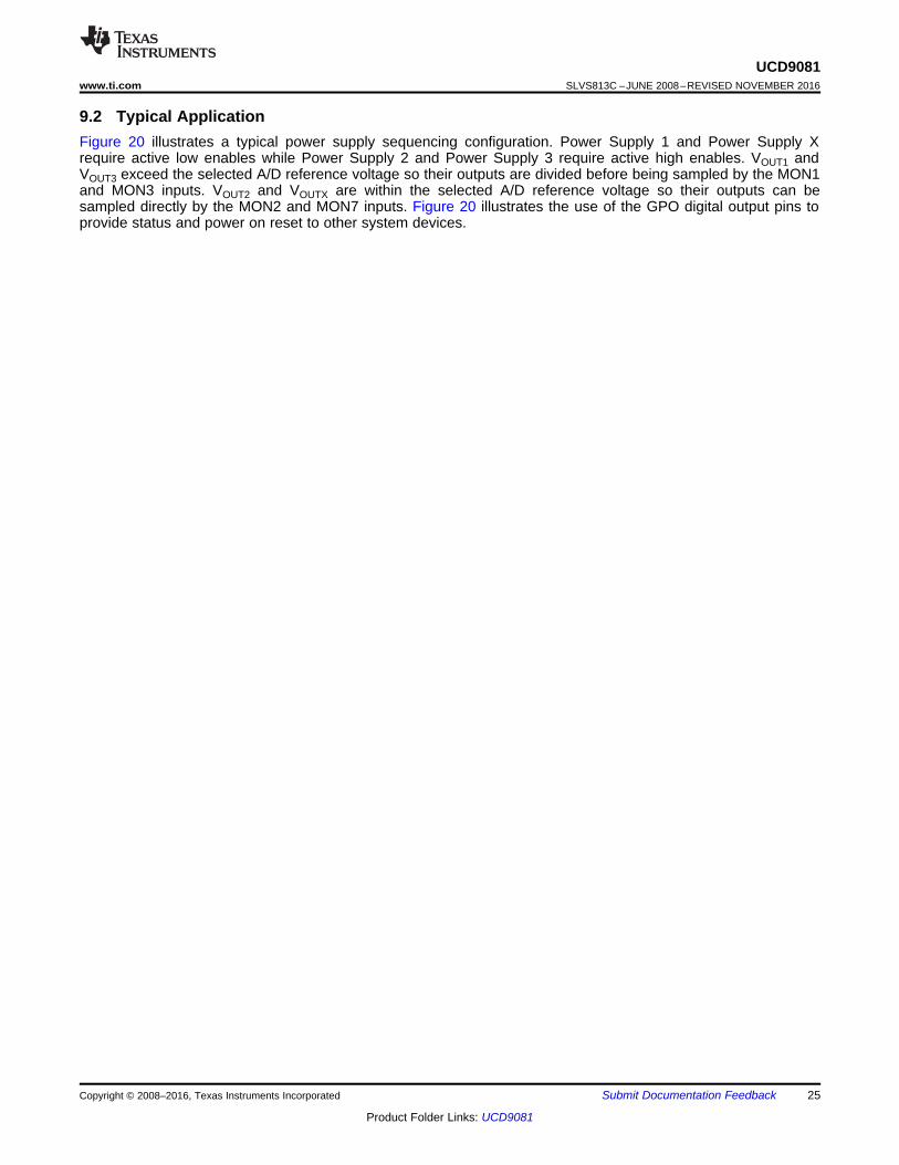
Figure 20 shows the UCD9081 power-supplysequencer in a typical application.
Device Information(1)
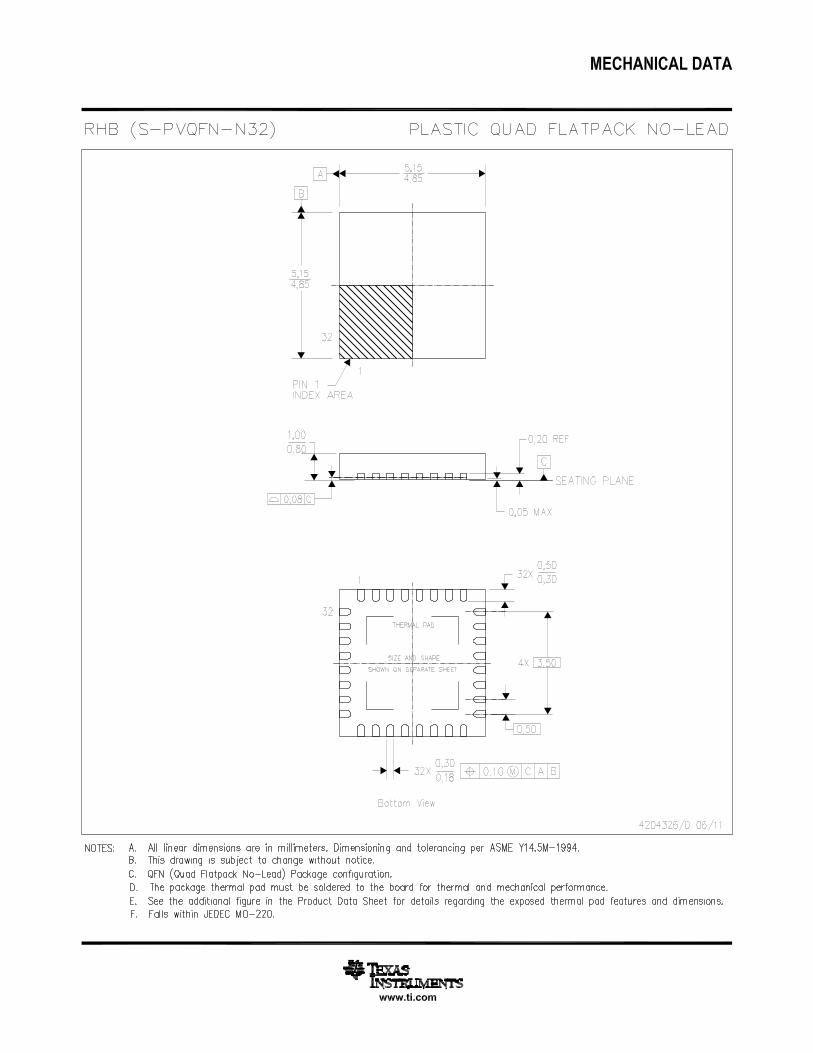
PART NUMBER PACKAGE BODY SIZE (NOM)UCD9081 VQFN (32) 5.00 mm × 5.00 mm
(1) For all available packages, see the orderable addendum atthe end of the data sheet.
Typical Application Diagram
2
UCD9081SLVS813C –JUNE 2008–REVISED NOVEMBER 2016 www.ti.com
Product Folder Links: UCD9081
Submit Documentation Feedback Copyright © 2008–2016, Texas Instruments Incorporated
Table of Contents1 Features .................................................................. 12 Applications ........................................................... 13 Description ............................................................. 14 Revision History..................................................... 25 Pin Configuration and Functions ......................... 36 Specifications......................................................... 5
6.1 Absolute Maximum Ratings ...................................... 56.2 Recommended Operating Conditions....................... 56.3 Thermal Information .................................................. 56.4 Electrical Characteristics........................................... 56.5 Timing Requirements: I2C Interface.......................... 66.6 Typical Characteristics .............................................. 7
7 Parameter Measurement Information .................. 88 Detailed Description .............................................. 9
8.1 Overview ................................................................... 98.2 Functional Block Diagram ......................................... 98.3 Feature Description................................................. 108.4 Device Functional Modes........................................ 11
8.5 Programming........................................................... 148.6 Register Maps ......................................................... 18
9 Application and Implementation ........................ 249.1 Application Information............................................ 249.2 Typical Application .................................................. 25
10 Power Supply Recommendations ..................... 2811 Layout................................................................... 28
11.1 Layout Guidelines ................................................. 2811.2 Layout Example .................................................... 28
12 Device and Documentation Support ................. 2912.1 Documentation Support ........................................ 2912.2 Receiving Notification of Documentation Updates 2912.3 Community Resources.......................................... 2912.4 Trademarks ........................................................... 2912.5 Electrostatic Discharge Caution............................ 2912.6 Glossary ................................................................ 29
13 Mechanical, Packaging, and OrderableInformation ........................................................... 29
4 Revision HistoryNOTE: Page numbers for previous revisions may differ from page numbers in the current version.
Changes from Revision B (December 2010) to Revision C Page
• Added ESD Ratings table, Feature Description section, Device Functional Modes, Application and Implementationsection, Power Supply Recommendations section, Layout section, Device and Documentation Support section, andMechanical, Packaging, and Orderable Information section .................................................................................................. 1
• Deleted Ordering Information table; see POA at the end of the data sheet........................................................................... 1• Added Thermal Information table ........................................................................................................................................... 5• Moved Timing Parameters for I2C Interface table and I2C Timing diagram to Specifications ................................................ 6• Moved content in Monitoring the UCD9081 to Register Maps ............................................................................................. 18
Changes from Revision A (September 2008) to Revision B Page
• Added Note 1 to the PIN FUNCTIONS table ......................................................................................................................... 3• Added Note regarding state of enable and digital I/O pins when the device contains factory configuration ....................... 15• Added a reference to the UCD9081 Programming Guide.................................................................................................... 16
Changes from Original (June 2008) to Revision A Page
• Changed the data sheet from Product Preview to Production; multiple changes throughout................................................ 1• Changed first RAIL voltage equation From: × VREF To: × VR+ ............................................................................................. 19• Changed second RAIL voltage equation From: × VREF To: × VR+ ....................................................................................... 19
32R
OS
C9
MO
N6
1VSS 24 EN2
31N
C10
EN
42NC 23 EN1
30V
CC
11
EN
33XIN 22 SCL
29T
ES
T12
EN
54NC 21 SDA
28A
DD
R4/
GP
O4
13E
N6
5RST 20 NC
27A
DD
R3/
GP
O3
14E
N7
6MON1 19 MON5
26A
DD
R2/
GP
O2
15M
ON
77MON2 18 MON4
25E
N8/
AD
DR
1/G
PO
116
MO
N8
8MON3 17 NC
Not to scale
PowerPAD
3
UCD9081www.ti.com SLVS813C –JUNE 2008–REVISED NOVEMBER 2016
Product Folder Links: UCD9081
Submit Documentation FeedbackCopyright © 2008–2016, Texas Instruments Incorporated
(1) Enable and GPIO pins are in high-impedance state when a device is received from factory and during the first configurationprogramming done by customer.
5 Pin Configuration and Functions
RHB Package32-Pin VQFN
Top View
Pin FunctionsPIN (1)
I/O DESCRIPTIONNAME NO.ADDR2/GPO2 26 I/O I2C address select 2, general-purpose digital output 2ADDR3/GPO3 27 I/O I2C address select 3, general-purpose digital output 3ADDR4/GPO4 28 I/O I2C address select 4, general-purpose digital output 4EN1 23 I/O Voltage rail 1 enable (digital output)EN2 24 I/O Voltage rail 2 enable (digital output)EN3 11 I/O Voltage rail 3 enable (digital output)EN4 10 I/O Voltage rail 4 enable (digital output)EN5 12 I/O Voltage rail 5 enable (digital output)EN6 13 I/O Voltage rail 6 enable (digital output)EN7 14 I/O Voltage rail 7 enable (digital output)EN8/ADDR1/GPO1 25 I/O Voltage rail 8 enable (digital output), I2C address select 1, general-purpose digital output 1
MON1 6 I Analog input for voltage rail 1MON2 7 I Analog input for voltage rail 2MON3 8 I Analog input for voltage rail 3MON4 18 I Analog input for voltage rail 4
4
UCD9081SLVS813C –JUNE 2008–REVISED NOVEMBER 2016 www.ti.com
Product Folder Links: UCD9081
Submit Documentation Feedback Copyright © 2008–2016, Texas Instruments Incorporated
Pin Functions (continued)PIN (1)
I/O DESCRIPTIONNAME NO.MON5 19 I Analog input for voltage rail 5MON6 9 I Analog input for voltage rail 6MON7 15 I Analog input for voltage rail 7MON8 16 I Analog input for voltage rail 8NC 2 — Do not connect
NC 4, 17,20, 31 — Recommended to connect to VSS, pin is not connected internally
ROSC 32 — Internal oscillator frequency adjust. Must use 100-kΩ pullup to VCC for minimum drift and maximumfrequency when sampling voltage rails.
RST 5 I Reset inputSCL 22 I/O I2C clock. Must pull up to 3.3 V.SDA 21 I/O I2C data. Must pull up to 3.3 V.TEST 29 I Connect to VSS
VCC 30 — Supply voltageVSS 1 — Ground referenceXIN 3 — Connect to VCC
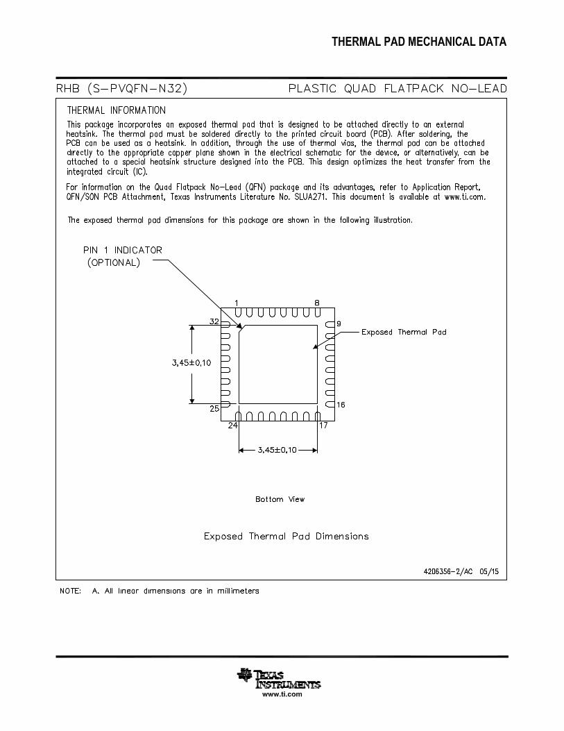
PowerPAD™ — — Package pad. Recommended to connect to VSS.
5
UCD9081www.ti.com SLVS813C –JUNE 2008–REVISED NOVEMBER 2016
Product Folder Links: UCD9081
Submit Documentation FeedbackCopyright © 2008–2016, Texas Instruments Incorporated
(1) Stresses beyond those listed under Absolute Maximum Ratings may cause permanent damage to the device. These are stress ratingsonly, which do not imply functional operation of the device at these or any other conditions beyond those indicated under RecommendedOperating Conditions. Exposure to absolute-maximum-rated conditions for extended periods may affect device reliability.
(2) All voltages referenced to VSS.
6 Specifications
6.1 Absolute Maximum Ratingsover operating free-air temperature range (unless otherwise noted) (1)
MIN MAX UNITVoltage applied from VCC to VSS –0.3 4.1 VVoltage applied to any pin (2) –0.3 VCC + 0.3 VESD diode current at any device terminal ±2 mAStorage temperature, Tstg –40 85 °C
6.2 Recommended Operating ConditionsMIN NOM MAX UNIT
VCC Supply voltage during operation and configuration changes 3 3.3 3.6 VTA Operating free-air temperature –40 85 °C
(1) For more information about traditional and new thermal metrics, see the Semiconductor and IC Package Thermal Metrics applicationreport.
6.3 Thermal Information
THERMAL METRIC (1)UCD9081
UNITRHB (VQFN)32 PINS
RθJA Junction-to-ambient thermal resistance 32.1 °C/WRθJC(top) Junction-to-case (top) thermal resistance 18.1 °C/WRθJB Junction-to-board thermal resistance 6 °C/WψJT Junction-to-top characterization parameter 0.2 °C/WψJB Junction-to-board characterization parameter 5.9 °C/WRθJC(bot) Junction-to-case (bottom) thermal resistance 1.2 °C/W
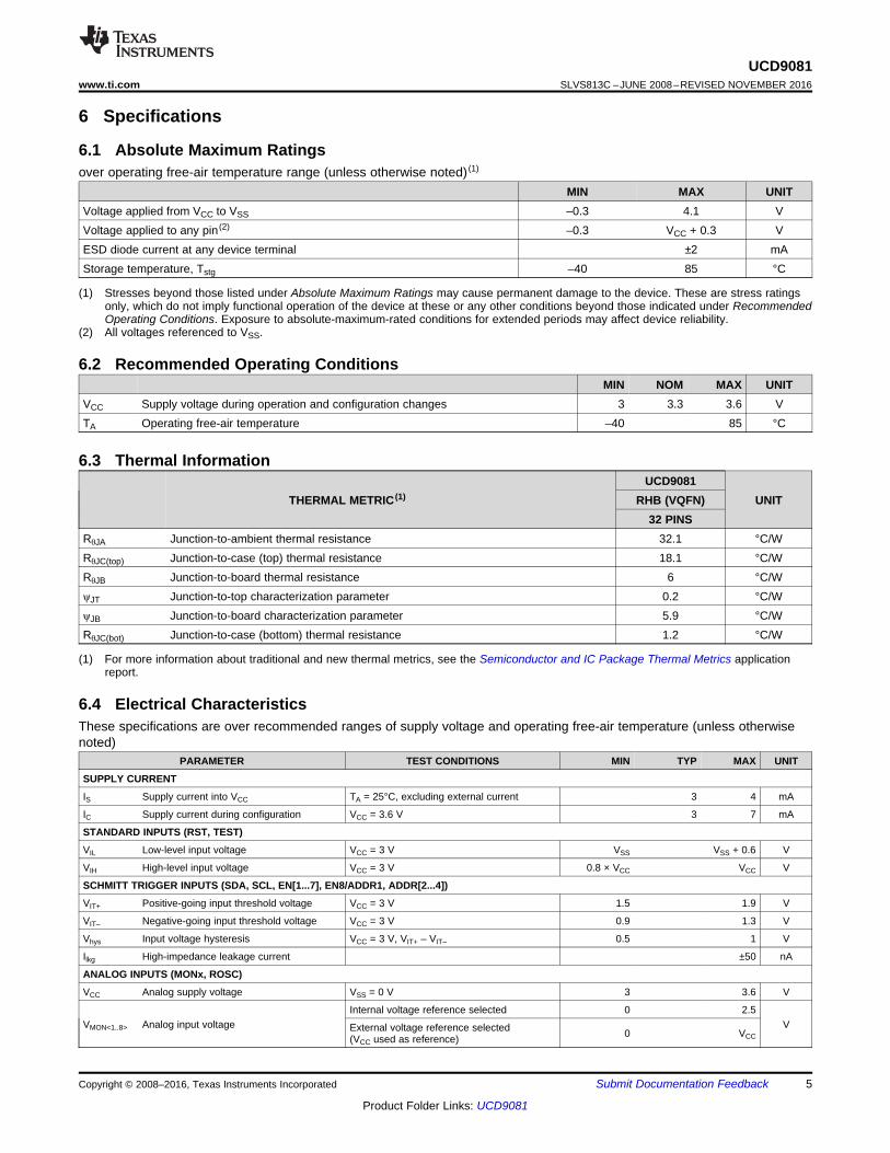
6.4 Electrical CharacteristicsThese specifications are over recommended ranges of supply voltage and operating free-air temperature (unless otherwisenoted)
PARAMETER TEST CONDITIONS MIN TYP MAX UNIT
SUPPLY CURRENT
IS Supply current into VCC TA = 25°C, excluding external current 3 4 mA
IC Supply current during configuration VCC = 3.6 V 3 7 mA
STANDARD INPUTS (RST, TEST)
VIL Low-level input voltage VCC = 3 V VSS VSS + 0.6 V
VIH High-level input voltage VCC = 3 V 0.8 × VCC VCC V
SCHMITT TRIGGER INPUTS (SDA, SCL, EN[1...7], EN8/ADDR1, ADDR[2...4])
VIT+ Positive-going input threshold voltage VCC = 3 V 1.5 1.9 V
VIT– Negative-going input threshold voltage VCC = 3 V 0.9 1.3 V
Vhys Input voltage hysteresis VCC = 3 V, VIT+ – VIT– 0.5 1 V
Ilkg High-impedance leakage current ±50 nA
ANALOG INPUTS (MONx, ROSC)
VCC Analog supply voltage VSS = 0 V 3 3.6 V
VMON<1..8> Analog input voltageInternal voltage reference selected 0 2.5
VExternal voltage reference selected(VCC used as reference) 0 VCC
6
UCD9081SLVS813C –JUNE 2008–REVISED NOVEMBER 2016 www.ti.com
Product Folder Links: UCD9081
Submit Documentation Feedback Copyright © 2008–2016, Texas Instruments Incorporated
Electrical Characteristics (continued)These specifications are over recommended ranges of supply voltage and operating free-air temperature (unless otherwisenoted)
PARAMETER TEST CONDITIONS MIN TYP MAX UNIT
(1) Not production tested. Limits verified by design.(2) The current consumption of the brown-out module is already included in the ICC current consumption data.(3) During power up, device initialization starts following a period of td(BOR) after VCC = V(B_IT–) + Vhys(B_IT–).(4) The maximum total current, IOHmax and IOLmax, for all outputs combined, must not exceed ±12 mA to hold the maximum voltage drop
specified.(5) The maximum total current, IOHmax and IOLmax, for all outputs combined, must not exceed ±48 mA to hold the maximum voltage drop
specified.
CI(1) Input capacitance Only one terminal can be selected at a time
(MON1 to MON8) 27 pF
RI(1) Input MUX ON resistance 0 V ≤ VMONx ≤ VCC, VCC = 3 V 2000 Ω
Ilkg High-impedance leakage current MON1 to MON8 ±50 nA
VREF+ Positive internal reference voltage Internal voltage reference selected,VCC = 3 V 2.35 2.5 2.65 V
VTUE ADC total unadjusted error VCC = 3 V
VR+ = 2.5 V(internal reference) ±12.2
mVVR+ = VCC(external reference) ±14.7
TREF+(1) Temperature coefficient of internal voltage
referenceI(VREF+) is a constant in the range of0 mA ≤ I(VREF+) ≤ 1 mA, VCC = 3 V ±100 ppm/°C
MISCELLANEOUS
Tretention Retention of configuration parameters TJ = 25°C 100 Years
POR, BROWNOUT, RESET (2) (3)
td(BOR) Brownout 2000 µs
VCC(start) Brownout dVCC/dt ≤ 3 V/s 0.7 × V(B_IT–) V
V(B_IT–) Brownout dVCC/dt ≤ 3 V/s 1.71 V
Vhys(B_IT–) Brownout dVCC/dt ≤ 3 V/s 70 130 180 mV
t(reset) Brownout Pulse length required at RST pin to acceptreset internally, VCC = 3 V 2 µs
DIGITAL OUTPUTS (EN8/GPO1, GPO[2...4], EN[1...7], SDA, SCL)
VOH High-level output voltageIOHmax = –1.5 mA (4), VCC = 3 V VCC – 0.25 VCC
VIOHmax = –6 mA (5), VCC = 3 V VCC – 0.6 VCC
VOL Low-level output voltageIOLmax = 1.5 mA (4), VCC = 3 V VSS VSS + 0.25
VIOLmax = 6 mA (5), VCC = 3 V VSS VSS + 0.6
Ilkg High-impedance leakage current VCC = 3 V ±50 nA
(1) See Electrical Characteristics(2) The maximum tf for the SDA and SCL bus lines (300 ns) is longer than the specified maximum tof for the output stages (250 ns). This
allows series protection resistors, Rs , to be connected between the SDA/SCL pins and the SDA/SCL bus lines without exceeding themaximum specified tf.
(3) A device must internally provide a hold time of at least 300 ns for the SDA signal to bridge the undefined region of the falling edge ofSCL.
(4) The maximum tHD;DAT must only be met if the device does not stretch the LOW period (tLOW) of the SCL signal.
6.5 Timing Requirements: I2C InterfaceMIN MAX UNIT
tofof Output fall time from VOH to VOL(1) with a bus capacitance from 10 pF to 400 pF 250 (2) ns
CI Capacitance for each pin 10 pFfSCL SCL clock frequency 10 100 kHztHD;STA Repeated hold time START condition (after this period, the first clock pulse is generated) 4 µstHD;DAT Data hold time 0 (3) 3.45 (4) µstLOW LOW period of the SCL clock 4.7 µstHIGH HIGH period of the SCL clock 4 µstSU;STA Setup time for repeated start condition 4.7 µstSU;DAT Data setup time 250 ns
V − High-Level Output Voltage − VOH
10−
3
ITyp
ical H
igh
-Level O
utp
ut
Cu
rren
tm
AO
H−
−
V = 3 V
P1.0CC
T = 85 CAo
T = 25 CAo
0 0.5 1 1.5 2 3.52.5
−30
0
−50
−20
−60
−40
V − Low-Level Output Voltage − VOL
10
3
ITyp
ical L
ow
-Level O
utp
ut
Cu
rren
tm
AO
L−
−
V = 3 V
P1.0CC
T = 85 CAo
T = 25 CAo
0 0.5 1 1.5 2 3.52.5
30
0
50
20
40
S
SDA
SCL
SPSr
tr
tSU;STO
tBUFtHD;STA
tSU;STA
tr
tHIGH
tHD;DAT
tSU;DAT
tHD;STA
tLOW
tf
tof
7
UCD9081www.ti.com SLVS813C –JUNE 2008–REVISED NOVEMBER 2016
Product Folder Links: UCD9081
Submit Documentation FeedbackCopyright © 2008–2016, Texas Instruments Incorporated
Timing Requirements: I2C Interface (continued)MIN MAX UNIT
tr Rise time of both SDA and SCL signals 1000 nstf Fall time of both SDA and SCL signals 300 nstSU;STO Setup time for STOP condition 4 µstBUF Bus free time between a STOP and START condition 4.7 µsC(b) Capacitive load for each bus line 400 pFVnL Noise margin at the LOW level for each connected device (including hysteresis) 0.1 × VDD VVnH Noise margin at the HIGH level for each connected device (including hysteresis) 0.2 × VDD V
Figure 1. Timing Diagram for I2C Interface
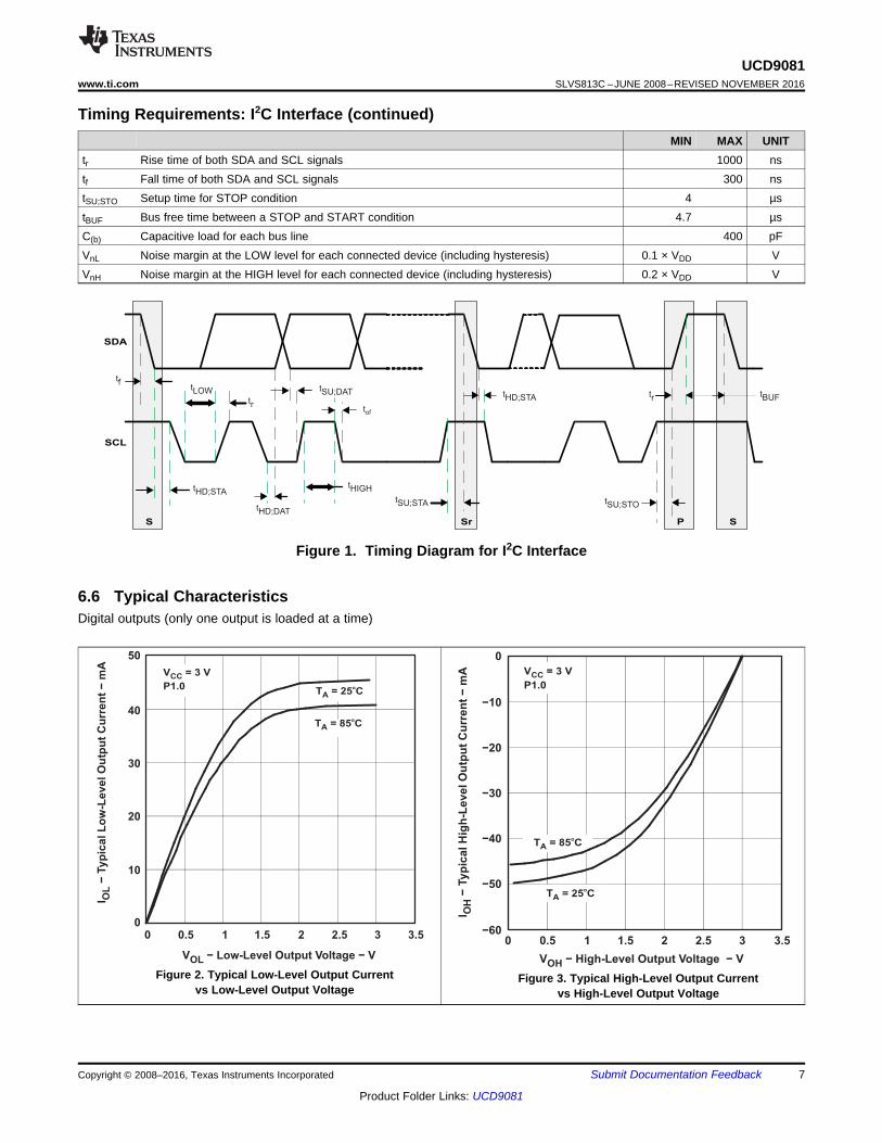
6.6 Typical CharacteristicsDigital outputs (only one output is loaded at a time)
Figure 2. Typical Low-Level Output Currentvs Low-Level Output Voltage
Figure 3. Typical High-Level Output Currentvs High-Level Output Voltage
V = 3 V
Typical ConditionsCC
VV
CC
(min
)-
t Pulse Width Spw - - mt Pulse Width spw - - m
tpw
t tfall = rise
tfall trise
VCC
VCC(min)
3 V2
1
1.5
1000
0
0.5
0.001 1
V = 3 V
Typical ConditionsCC
VV
CC
(min
)-
t Pulse Width Spw - - m
t Pulse Width Spw - - m
tpwVCC
VCC(min)
3 V
1 ns
2
1
1.5
1000
0
0.5
0.001 1
1 ns
0
1
VCC
V(B_IT–)
Vhys(B_IT–)
VCC(start)
td(BOR)
Set signal forPOR circuitry
8
UCD9081SLVS813C –JUNE 2008–REVISED NOVEMBER 2016 www.ti.com
Product Folder Links: UCD9081
Submit Documentation Feedback Copyright © 2008–2016, Texas Instruments Incorporated
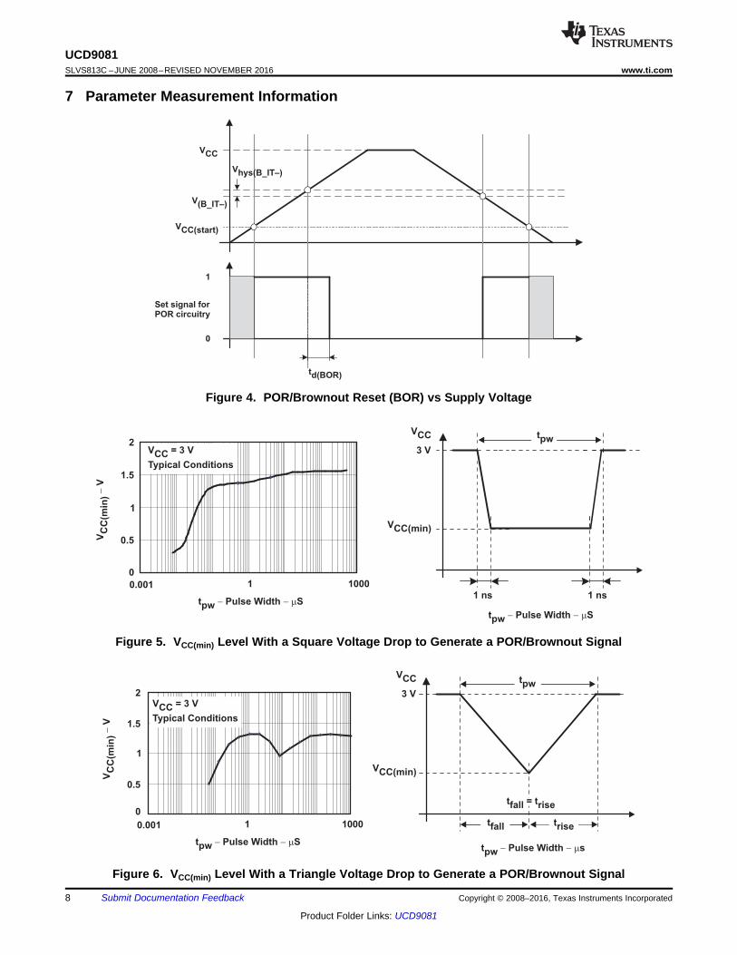
7 Parameter Measurement Information
Figure 4. POR/Brownout Reset (BOR) vs Supply Voltage
Figure 5. VCC(min) Level With a Square Voltage Drop to Generate a POR/Brownout Signal
Figure 6. VCC(min) Level With a Triangle Voltage Drop to Generate a POR/Brownout Signal
MON1MON2
MON3
MON4
MON5MON6
MON7
MON8
Oscillator
StatusRegisters
10-bitSAR ADC
I CEngine
2
PowerEnables
EN1
EN2
EN3EN4
EN5
EN6
EN7
EN8/GPO1General-PurposeOutputs
GPO2
GPO3
GPO4Config
Memory
Error LogFlash
Memory
SCL SDA
AnalogInputs
SequencingEngine
Copyright © 2016, Texas Instruments Incorporated
9
UCD9081www.ti.com SLVS813C –JUNE 2008–REVISED NOVEMBER 2016
Product Folder Links: UCD9081
Submit Documentation FeedbackCopyright © 2008–2016, Texas Instruments Incorporated
8 Detailed Description
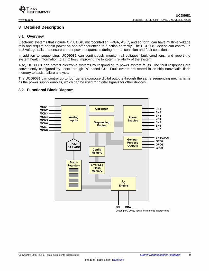
8.1 OverviewElectronic systems that include CPU, DSP, microcontroller, FPGA, ASIC, and so forth, can have multiple voltagerails and require certain power on and off sequences to function correctly. The UCD9081 device can control upto 8 voltage rails and ensure correct power sequences during normal condition and fault conditions.
In addition to sequencing, UCD9081 can continuously monitor rail voltages, fault conditions, and report thesystem health information to a I2C host, improving the long-term reliability of the system.
Also, UCD9081 can protect electronic systems by responding to power system faults. The fault responses areconveniently configured by users through PC-based GUI. Fault events are stored in on-chip nonvolatile flashmemory to assist failure analysis.
The UCD9081 can control up to four general-purpose digital outputs through the same sequencing mechanismsas the power supply enables, which can be used for digital signals for other devices.
8.2 Functional Block Diagram
10
UCD9081SLVS813C –JUNE 2008–REVISED NOVEMBER 2016 www.ti.com
Product Folder Links: UCD9081
Submit Documentation Feedback Copyright © 2008–2016, Texas Instruments Incorporated
8.3 Feature Description
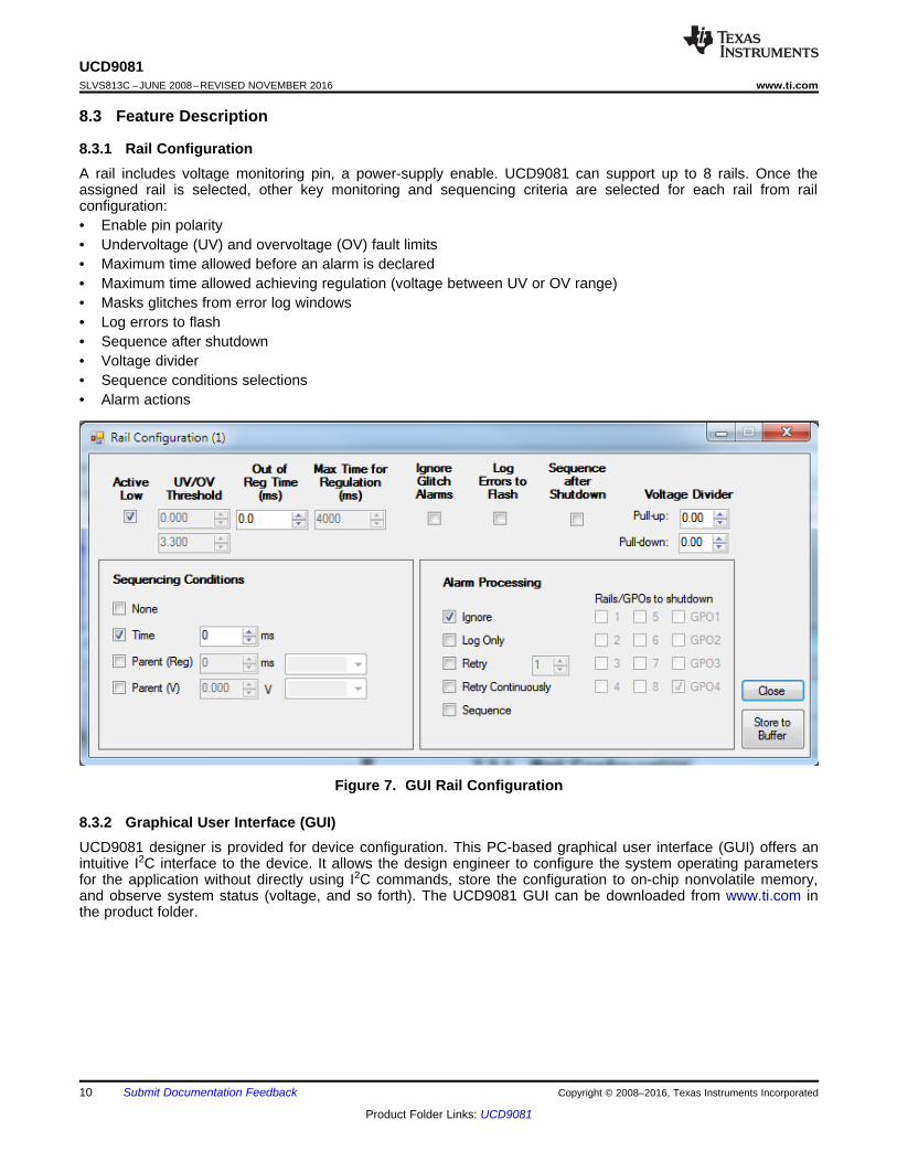
8.3.1 Rail ConfigurationA rail includes voltage monitoring pin, a power-supply enable. UCD9081 can support up to 8 rails. Once theassigned rail is selected, other key monitoring and sequencing criteria are selected for each rail from railconfiguration:• Enable pin polarity• Undervoltage (UV) and overvoltage (OV) fault limits• Maximum time allowed before an alarm is declared• Maximum time allowed achieving regulation (voltage between UV or OV range)• Masks glitches from error log windows• Log errors to flash• Sequence after shutdown• Voltage divider• Sequence conditions selections• Alarm actions
Figure 7. GUI Rail Configuration
8.3.2 Graphical User Interface (GUI)UCD9081 designer is provided for device configuration. This PC-based graphical user interface (GUI) offers anintuitive I2C interface to the device. It allows the design engineer to configure the system operating parametersfor the application without directly using I2C commands, store the configuration to on-chip nonvolatile memory,and observe system status (voltage, and so forth). The UCD9081 GUI can be downloaded from www.ti.com inthe product folder.
11
UCD9081www.ti.com SLVS813C –JUNE 2008–REVISED NOVEMBER 2016
Product Folder Links: UCD9081
Submit Documentation FeedbackCopyright © 2008–2016, Texas Instruments Incorporated
8.4 Device Functional Modes
8.4.1 Power Supply SequencingThe UCD9081 can be configured to sequence power supply rails using the enable signals (ENx) or the general-purpose outputs (GPOx) in one of four ways:
1. A rail can be configured to not be sequenced2. Using a delay time after UCD9081 RESET. The enable or GPO is asserted after UCD9081 RESET plus the
user specified delay3. Using a delay time after another (parent) rail has achieved regulation (VRAIL is within specified under- and
overvoltage settings). The enable or GPO is asserted after the (parent) rail is in regulation plus the userspecified delay.
4. Using a (parent) rail voltage. The enable or GPO is asserted after the (parent) rail voltage is greater than orequal to the user specified voltage.
8.4.2 Power-Supply EnablesThe UCD9081 can sequence and enable or disable up to eight power supplies through the ENx (EN1 to EN8)signals. These signals can be configured active-high or active-low, supporting power supplies with either polarity.
EN8 can also be configured as a GPO (GPO1). EN8/ADDR1/GPO1 is also used for I2C address selection(ADDR1).
While the UCD9081 is in RESET, the enable signals are in a high-impedance state. The enable signals must bepulled up or down on the board according to the desired default power-supply state (enabled or disabled).
8.4.3 General-Purpose OutputsThe UCD9081 can control up to four general-purpose digital outputs through the same sequencing mechanismsas the power supply enables. These general-purpose outputs (GPO1–GPO4) can be used for digital signals suchas resets or status inputs to other devices. These signals are multiplexed with other functions (primarily I2Caddress selection). See Pin Configuration and Functions to ensure that these signals are used properly by theapplication. The GPO1 signal is also multiplexed with EN8.
8.4.4 Device ResetUCD9081 RESET occurs due to one of the following conditions:
• External RST pin is asserted• Power is applied to the device (power-on-reset) or power is cycled• A sequence event occurs as a result of a configured rail alarm event• RESTART command is issued over the I2C bus
During RESET, the following takes place:
• All ENx and GPOx pins are placed in a high-impedance state• All internal timers are reset to zero• The I2C address pins (ADDR1-ADDR4) are sampled and the device address is assigned accordingly• All ENx and GPOx pins are driven to their inactive levels• The UCD9081 runs a checksum function to validate its memory contents• If there are no errors, the device starts sequencing according to the current sequencer configuration
During this time, the UCD9081 does not respond to host requests made over the I2C bus.
To ensure the integrity of data within the device, the device runs a checksum function during RESET. If theconfiguration parameters of the device are valid, the UCD9081 begins operating according to the currentsequencer configuration. If the configuration parameters are invalid, the UCD9081 overwrites the currentconfiguration parameters with the last known good configuration and the device begins operating with theseparameters. This can cause a delay in the RESET time. To establish a copy of the valid configuration, UCD9081RESET time is delayed the first time a new configuration is loaded.
12
UCD9081SLVS813C –JUNE 2008–REVISED NOVEMBER 2016 www.ti.com
Product Folder Links: UCD9081
Submit Documentation Feedback Copyright © 2008–2016, Texas Instruments Incorporated
Device Functional Modes (continued)8.4.5 Voltage ReferenceThe analog to digital converter in the UCD9081 has a selectable voltage reference, VR+. The voltage referencecan either be an internally generated 2.5-V reference or an external reference derived from VCC. The externalreference is recommended for those systems requiring more accurate voltage readings. See EstimatingUCD9081 Reporting Accuracy Over Variations in ADC Voltage Reference for information on calculating theaccuracy of each reference.
8.4.6 Voltage MonitoringThe UCD9081 can monitor eight voltage rails through the MONx terminals of the device (MON1 to MON8). TheUCD9081 samples these eight input channels and uses the selected reference to convert the voltages to digitalvalues. These values are accessible through the I2C interface. When monitoring a voltage rail that has a nominalvoltage larger than the selected reference, a resistor divider network is typically used. The design must ensurethat the source impedance of the resistor network is chosen properly to maintain the accuracy of the analog todigital conversion. For more details, see Application Information.
The UCD9081 allows the user to independently specify the following for each monitored rail:
• overvoltage (OV) threshold• undervoltage (UV) threshold• out of regulation time or glitch width (OORW)• maximum time for regulation (MTFR)
The MTFR is used to determine whether or not a rail starts successfully after being enabled.
The UCD9081 also has the ability to ignore glitches. Glitches are fault conditions that last less than the specifiedOORW for that rail. Ignoring glitches may be useful in the case where the power supply is known to be noisy butstill operates well. Ignoring glitches does not affect the monitoring capability of the UCD9081 with respect todetecting sustained UV or OV faults. It simply prevents the UCD9081 from logging glitch faults to the error log.
8.4.7 Rail ShutdownRail (or GPO) shutdown is the act of setting the ENx (or GPOx) pin to a state which disables the associatedpower supply output. A rail can shutdown for one of the following reasons:
• A fault condition on the rail itself• A fault condition on a parent rail resulting in a shutdown• An I2C shutdown command
Each rail and GPO can be independently configured to shutdown according to a user-specified time delay from0 ms to 4095 ms. This is referred to as the system shutdown configuration.
8.4.8 Alarm ProcessingEach rail can be independently configured to respond to an alarm or fault in a variety of ways. A fault can be anUV condition, OV condition, or a rail that did not start (MTFR exceeded before UV threshold achieved). Theoptions for alarm processing are as follows:• Ignore• Log only• Retry n times (n = 0,1,2,3,4)• Retry continuously• Sequence (immediately)• Sequence after shutdown
In addition to these options, a rail can be independently configured to log errors to FLASH to aid in failureanalysis. For more details, see Error Logging.
13
UCD9081www.ti.com SLVS813C –JUNE 2008–REVISED NOVEMBER 2016
Product Folder Links: UCD9081
Submit Documentation FeedbackCopyright © 2008–2016, Texas Instruments Incorporated
Device Functional Modes (continued)8.4.8.1 IgnoreThe UCD9081 can be configured to ignore all alarms on the rail. This is the recommended option for all unusedpower supply rails on the UCD9081.
8.4.8.2 Log OnlyThe UCD9081 can be configured to log a fault and take no additional action. For more information, see ErrorLogging.
8.4.8.3 Retry n TimesThe UCD9081 can be configured to attempt to restart a rail up to n times (n = 0,1,2,3, or 4) in response to asustained fault condition. With this option, the user can also specify which rails and GPOs are dependent uponthe configured rail. When a sustained fault is detected, the faulty rail is disabled and re-enabled the desirednumber of times. The rail remains enabled for the specified MTFR before attempting another retry. If the rail doesnot achieve regulation after the desired number of retries, all user-specified dependent rails and GPOs areshutdown according to the times specified in the system shutdown configuration. If any of the dependent railshave other rails or GPOs marked as dependents, those dependent rails or GPOs are also forced to shutdownregardless of their alarm processing configurations.
8.4.8.4 Retry ContinuouslyThe UCD9081 can be configured to continuously attempt to restart a faulty rail. When the UCD9081 detects asustained fault condition on the configured rail, the rail is disabled and then re-enabled. The rail remains enabledfor the specified MTFR. The retry process repeats for this rail until it properly achieves regulation.
8.4.8.5 SequenceThe UCD9081 can be configured to sequence the entire system in response to a sustained fault condition. Whenthe UCD9081 detects a fault on the configured rail, all rails and GPOs are shutdown immediately and UCD9081RESET occurs (see Device Reset). For this configuration, a shutdown according to the delay times specified bythe system shutdown configuration does not occur prior to UCD9081 RESET.
8.4.8.6 Sequence After ShutdownSequence after shutdown is an option that can be used in conjunction with Retry n Times. When a fault occurson the configured rail, this option forces a UCD9081 RESET to occur after the procedure outlined in Retry nTimes takes place. If a rail is configured for sequence after shutdown and is forced to shutdown due to a fault ona parent rail, a sequence after shutdown takes place.
8.4.9 Error LoggingThe UCD9081 is capable of logging errors in two ways. The first method uses an eight-deep FIFO located involatile memory (SRAM) of the UCD9081. Error conditions are posted to the ERROR registers according to theconfiguration for that rail. The UCD9081 logs the type of error, the time (from Reset) when the error occurred, therail number, and the rail voltage. If the user has specified ignore glitches as an option for the faulty rail, glitchesare not posted to the error log. If the user has specified Ignore as the alarm response for the faulty rail, no errorsare posted to the error log for that rail. All other alarm responses result in the error condition being logged. Dueto the unknown latency of the host extracting data from the FIFO, the UCD9081 only posts to the FIFO is if it hasroom to write. There is no impact to the monitoring operation of the UCD9081 if this FIFO is full and cannot bewritten.
The second method of error logging uses the non-volatile memory (FLASH) of the UCD9081. Similar to the errorlog in SRAM, faults are posted for all rails that have the appropriate alarm processing options selected. In thiscase, errors are posted to both the SRAM log and the FLASH log. The UCD9081 is capable of recording up toeight entries in the flash error log. Again, the UCD9081 only posts to the log if there is room to write. There is noimpact to the monitoring operation of the UCD9081 if the error log is full and cannot be written.
14
UCD9081SLVS813C –JUNE 2008–REVISED NOVEMBER 2016 www.ti.com
Product Folder Links: UCD9081
Submit Documentation Feedback Copyright © 2008–2016, Texas Instruments Incorporated
Device Functional Modes (continued)To provide flexibility for a variety of systems, the UCD9081 has two modes for non-volatile error logging. The firstmode configures the UCD9081 to hold in RESET when entries are present in the FLASH error log. This isadvantageous in systems where a master I2C device is available to read the error log following a critical systemfailure. When configured for this mode, the UCD9081 checks for a non-empty FLASH error log during RESET. Ifthere are entries in the FLASH error log, the device waits for a host to clear the error log before sequencing thedevice. For information on clearing the FLASH error log, see the section on Resetting the Flash Error Log.
The second mode allows the UCD9081 to sequence (following a RESET of the device) regardless of whether ornot there are entries present in the FLASH error log. This is useful in systems with no master I2C device, orwhere power cycles are common and not due to system failure.
For information on reading the error logs in each mode, see Register Maps.
8.4.10 BrownoutThe brownout circuit is implemented to provide the proper internal reset signal to the device during power on andpower off.
8.5 Programming
8.5.1 I2C InterfaceThe UCD9081 power-supply sequencer has a 100 kHz, slave mode I2C interface for communication with an I2Cmaster. The I2C master uses this interface to configure and monitor the UCD9081. The master must supportclock stretching to properly communicate with the UCD9081.
8.5.2 Configuring and Monitoring the UCD9081The UCD9081 supports both configuration and monitoring using its I2C slave interface. A Microsoft Windows™GUI is available for configuring and monitoring the UCD9081. This GUI can be downloaded from the TI websiteat www.ti.com.
For monitoring the sequencer, an I2C memory map allows an I2C host to perform memory-mapped reads (and insome cases writes) to obtain status information from the UCD9081. For instance, all rails can report their voltagethrough the I2C memory map. For information on which parameters are available through the I2C memory map,see Register Maps.
To change configuration parameters of the sequencer, a different mechanism is used. The entire set ofconfiguration parameters must be written at one time to the device as one large transaction over the I2Cinterface. This ensures that the configuration of the device is consistent at any given time. The process forconfiguring the UCD9081 is described in Configuring the UCD9081.
The UCD9081 is compatible with 3.3-V IO ports of microcontrollers, TMS320™ DSP family as well as ASICs.The UCD9081 is available in a plastic 32-pin VQFN package (RHB).
8.5.3 Resetting the Flash Error LogThe UCD9081 can be configured to log errors on a critical voltage rail to internal FLASH memory. Thismechanism permits the error log to be read after the device has been reset, or if a loss of power causes non-volatile memory to be cleared. As outlined in Error Logging, there are two modes for using this feature.
The first mode holds the UCD9081 in RESET (following a RESET of the device) if entries are present in theFLASH error log. This allows the user to successfully read and clear the FLASH error log before sequencing thesystem. When using this mode, the UCD9081 does not sequence until the FLASH error log is cleared. To clearthe FLASH error log and sequence the device, perform the following steps:
• Write FLASHLOCK register to a value of 0x02• Write WADDR register to a value of 0x1000• Write WDATA register to a value of 0xBADC• Write WADDR register to a value of 0x107E• Write WDATA register to a value of 0xBADC• Write FLASHLOCK register to a value of 0x00
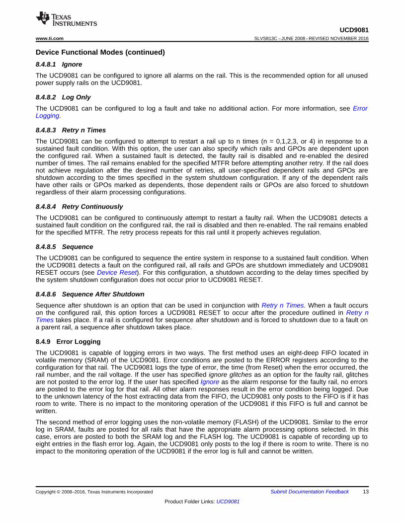
I2C Write:FLASHLOCK =UNLOCK (0x02)
I2C Write:WADDR =
0xE000
I2C Write:WDATA =0xBADC
I2C Write:WADDR =
0xE000
I2C Write:WDATA =Data (16b)
I2C Write:WDATA =Data (16b)
I2C Write:FLASHLOCK =LOCK (0x00)
. . .
Up to 16 times (32 bytes)
- OR -
Repeat as necessary with WADDR updatedto write 512 bytes
15
UCD9081www.ti.com SLVS813C –JUNE 2008–REVISED NOVEMBER 2016
Product Folder Links: UCD9081
Submit Documentation FeedbackCopyright © 2008–2016, Texas Instruments Incorporated
Programming (continued)• Write RESTART register to a value of 0x00
The second mode allows the UCD9081 to sequence (following a RESET of the device) regardless of whether ornot there are entries present in the FLASH error log. When using this mode, the user still may wish to clear theFLASH error logs some time after RESET. To do this, perform the following steps:
• Write FLASHLOCK register to a value of 0x02• Write WADDR register to a value of 0x1000• Write WDATA register to a value of 0xBADC• Write WADDR register to a value of 0x107E• Write WDATA register to a value of 0xBADC• Write FLASHLOCK register to a value of 0x00
Clearing the FLASH error log during run-time causes a delay in monitoring.
8.5.4 Configuring the UCD9081The UCD9081 has many different configurable parameters such as sequencing options, alarm processingoptions, and rail dependencies. A Microsoft Windows™ GUI is available for selecting and generating thenecessary configuration parameters. The UCD9081 GUI can be downloaded from www.ti.com in the productfolder. See UCD9081 EVM User's Guide (SLVU249) for details on installing and using the GUI. Once the user-specific configuration parameters are selected, the GUI generates a hex file that can be loaded into the flashmemory of the UCD9081 through the I2C interface.
NOTEBecause loading a new configuration requires writing to FLASH memory, the UCD9081does not monitor the MONx inputs while the configuration parameters are being updated.
NOTEThe enable and digital I/O pins of the UCD9081 are in a high impedance state when thedevice is not configured (Texas instruments delivers the device in this state).
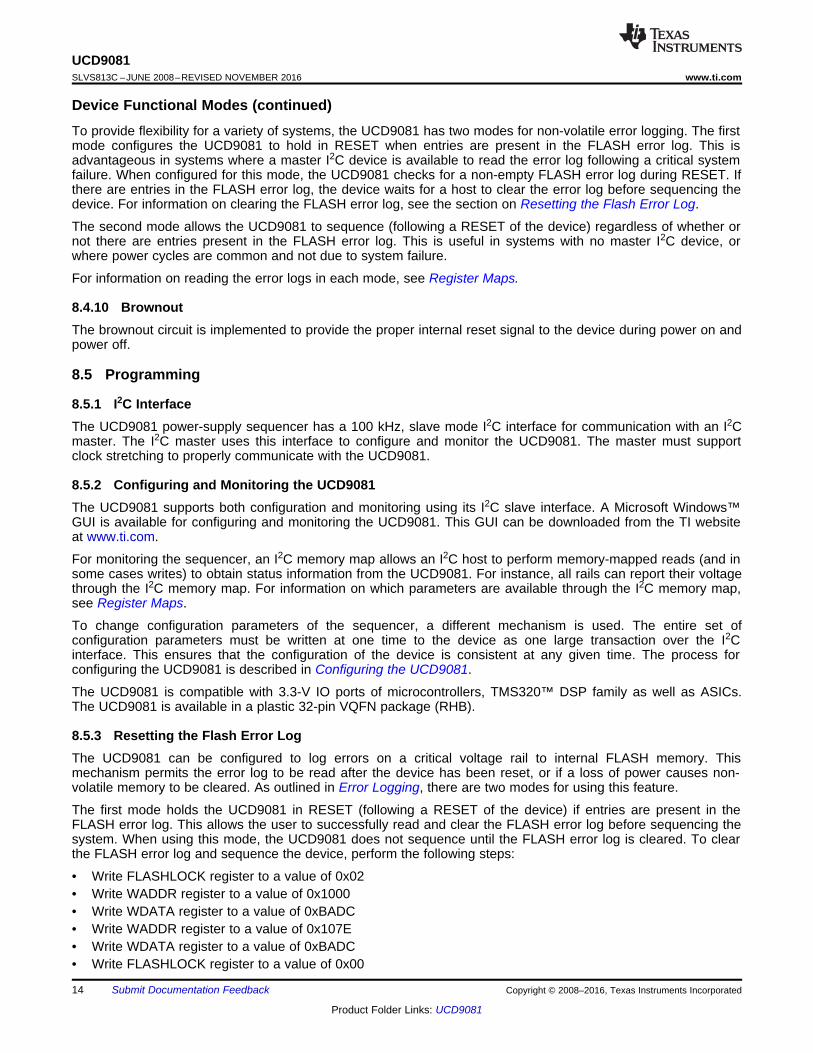
To download the configuration parameters generated by the GUI into the UCD9081, a contiguous block ofconfiguration information is sent to the device through the I2C interface. This block is 512 bytes long and starts ataddress 0xE000.
This 512-byte block of configuration information is sent to the device in multiple segments. The segment size canrange from 2 to 32 bytes at one time, and must be a multiple of 2 bytes. That is, a master can send 256 2-bytesegments or 32 16-byte segments, and so on. All the segments must be sent back-to-back in the propersequence, and this operation must be completed by sending the last segment so that the last byte of the512-byte block is written. If this is not done, the UCD9081 is in an unknown state and does not function asdesigned.
The process for sending the configuration information to the UCD9081 is as shown in Figure 8.
Figure 8. Configuration Information
16
UCD9081SLVS813C –JUNE 2008–REVISED NOVEMBER 2016 www.ti.com
Product Folder Links: UCD9081
Submit Documentation Feedback Copyright © 2008–2016, Texas Instruments Incorporated
Programming (continued)As shown in Figure 8, the process for updating the configuration of the UCD9081 is as follows:1. Unlock flash memory by writing the value 0x02 to the FLASHLOCK register2. Write the address of the configuration section of memory (WADDR = 0xE000)3. Write the constant 0xBADC to update memory (WDATA = 0xBADC)4. Write the address of the configuration section of memory again (WADDR = 0xE000)5. Write the data (WDATA = <varies>). Repeat steps 4 and 5 as necessary, depending on the data segment
size used, to write 512 bytes. Increment the address as necessary.6. Lock flash memory after the last byte of the last segment is written by writing the value 0x00 to the
FLASHLOCK register
At the conclusion of this process, the configuration of the UCD9081 is updated with the configuration changes, asrepresented by the values from the data segments. See UCD9081 Programming Guide (SLVA275) for moredetails on programming the UCD9081.
8.5.5 User DataUser data (128 bytes) can be stored in the UCD9081 FLASH memory at location 0x1080 to 0x10FF. Writes tothe User Data section of memory are performed as follows:
1. Unlock flash memory by writing the value 0x02 to the FLASHLOCK register2. Write the address of the USER DATA section of memory (WADDR = 0x1080)3. Write the constant 0xBADC to update memory (WDATA = 0xBADC)4. Write the address of the USER DATA section of memory again (WADDR = 0x1080)5. Write the data (WDATA = <varies>). Repeat steps 4 and 5 as necessary depending on the data segment
size used. Increment the address as necessary.6. Lock flash memory after the last byte of the last segment is written by writing the value 0x00 to the
FLASHLOCK register
To read the User Data section of memory, follow the procedure for reading memory outlined in WADDR andWDATA.
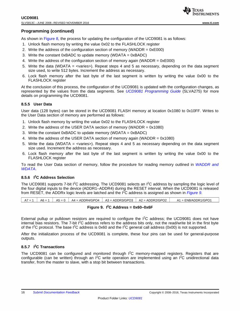
8.5.6 I2C Address SelectionThe UCD9081 supports 7-bit I2C addressing. The UCD9081 selects an I2C address by sampling the logic level ofthe four digital inputs to the device (ADDR1–ADDR4) during the RESET interval. When the UCD9081 is releasedfrom RESET, the ADDRx logic levels are latched and the I2C address is assigned as shown in Figure 9.
A7 = 1 A6 = 1 A5 = 0 A4 = ADDR4/GPO4 A3 = ADDR3/GPO3 A2 = ADDR2/GPO2 A1 = EN8/ADDR1/GPO1
Figure 9. I2C Address = 0x60–0x6F
External pullup or pulldown resistors are required to configure the I2C address; the UCD9081 does not haveinternal bias resistors. The 7-bit I2C address refers to the address bits only, not the read/write bit in the first byteof the I2C protocol. The base I2C address is 0x60 and the I2C general call address (0x00) is not supported.
After the initialization process of the UCD9081 is complete, these four pins can be used for general-purposeoutputs.
8.5.7 I2C TransactionsThe UCD9081 can be configured and monitored through I2C memory-mapped registers. Registers that areconfigurable (can be written) through an I2C write operation are implemented using an I2C unidirectional datatransfer, from the master to slave, with a stop bit between transactions.
S R/W R/WA
A P
From master to slave
From slave to master
Sr = Repeated START
SrSLAVE
ADDRESS
SLAVE
ADDRESS DATADATA
0 (write)
REGISTER
ADDRESS AA
AA
1 (read)
A/A
(n bytes +acknowledge)
A = acknowledge (SDA low)
= Not acknowledge (SDA high)A
S = START condition
P = STOP condition
1 7 1 1 8 1 8 1 11 7 1 1
SLAVE
ADDRESSR/W
REGISTER
ADDRESSDATAA A/A PA
From master to slave
From slave to master
A = acknowledge (SDA low)
= Not acknowledge (SDA high)A
S = START condition
P = STOP condition
1 7 1 1 8 1 8 1 1
0 (write)
S
17
UCD9081www.ti.com SLVS813C –JUNE 2008–REVISED NOVEMBER 2016
Product Folder Links: UCD9081
Submit Documentation FeedbackCopyright © 2008–2016, Texas Instruments Incorporated
8.5.7.1 I2C Unidirectional Transfer
Figure 10. I2C Register Access With START or STOP
Registers that can be read are implemented using an I2C read operation, which can use the I2C combined formatthat changes data direction during the transaction. This transaction uses an I2C repeated START during thedirection change.
8.5.7.2 I2C Combined Format
Figure 11. I2C Register Access With Repeated START
The UCD9081 also supports a feature that auto-increments the register address pointer for increased efficiencywhen accessing sequential blocks of data. It is not necessary to issue separate I2C transactions.
18
UCD9081SLVS813C –JUNE 2008–REVISED NOVEMBER 2016 www.ti.com
Product Folder Links: UCD9081
Submit Documentation Feedback Copyright © 2008–2016, Texas Instruments Incorporated
8.6 Register MapsThe UCD9081 allows all monitoring of the system through the I2C interface on the device. The following is thememory map of the supported registers in the system. The detail of each of these registers is given in the nextsection as well.
The UCD9081 supports functionality to increment the I2C register address value automatically when a register isbeing accessed to more efficiently access blocks of like registers. Table 1 also shows the amount that theregister address is incremented for each register access.
Table 1. Register Access AdjustmentREGISTER NAME ADDRESS ACCESS ADJUSTMENT AFTER ACCESS
RAIL1H 0x00 r +1 (0x01)RAIL1L 0x01 r +1 (0x02)RAIL2H 0x02 r +1 (0x03)RAIL2L 0x03 r +1 (0x04)RAIL3H 0x04 r +1 (0x05)RAIL3L 0x05 r +1 (0x06)RAIL4H 0x06 r +1 (0x07)RAIL4L 0x07 r +1 (0x08)RAIL5H 0x08 r +1 (0x09)RAIL5L 0x09 r +1 (0x0A)RAIL6H 0x0A r +1 (0x0B)RAIL6L 0x0B r +1 (0x0C)RAIL7H 0x0C r +1 (0x0D)RAIL7L 0x0D r +1 (0x0E)RAIL8H 0x0E r +1 (0x0F)RAIL8L 0x0F r –15 (0x00)
ERROR1 0x20 r +1 (0x21)ERROR2 0x21 r +1 (0x22)ERROR3 0x22 r +1 (0x23)ERROR4 0x23 r +1 (0x24)ERROR5 0x24 r +1 (0x25)ERROR6 0x25 r –5 (0x20)STATUS 0x26 r 0 (0x26)VERSION 0x27 r 0 (0x27)
RAILSTATUS1 0x28 r +1 (0x29)RAILSTATUS2 0x29 r –1 (0x28)FLASHLOCK 0x2E rw 0 (0x2E)
RESTART 0x2F w 0 (0x2F)WADDR1 0x30 rw +1 (0x31)WADDR2 0x31 rw –1 (0x30)WDATA1 0x32 rw +1 (0x33)WDATA2 0x33 rw –1 (0x32)
8.6.1 Register DescriptionsThe following are the detailed descriptions of each of the UCD9081 I2C registers.
The following register bit conventions are used. Each register is shown with a key indicating the accessibility ofeach bit, and the initial condition after device initialization.
PULLDOWN PULLUPV = VRAILn R+
PULLDOWN
RAILVn R + R
1024 Rx x
V = VRAILn R+
RAILVn
1024x
1 03 2458 67910111214 1315
r rr rrrr rrrr0r0r0r0 r0r0
RAILVn
19
UCD9081www.ti.com SLVS813C –JUNE 2008–REVISED NOVEMBER 2016
Product Folder Links: UCD9081
Submit Documentation FeedbackCopyright © 2008–2016, Texas Instruments Incorporated
8.6.2 RAILFor each of eight voltage rails, the UCD9081 has two registers that contain the rolling average voltage for theassociated rail as measured by the device. This average voltage is maintained in real-time by the UCD9081 andis calculated as the output of a 4-TAP FIR filter. There are two registers for each voltage rail. One holds theleast-significant 8 bits of the voltage and the other the most-significant 2 bits of the voltage. This is shown inTable 2.
Table 2. RAIL RegisterREGISTER NAME ADDRESS REGISTER CONTENTS
RAIL1H 0x00 RAIL1 voltage, bits 9:8RAIL1L 0x01 RAIL1 voltage, bits 7:0RAIL2H 0x02 RAIL2 voltage, bits 9:8RAIL2L 0x03 RAIL2 voltage, bits 7:0RAIL3H 0x04 RAIL3 voltage, bits 9:8RAIL3L 0x05 RAIL3 voltage, bits 7:0RAIL4H 0x06 RAIL4 voltage, bits 9:8RAIL4L 0x07 RAIL4 voltage, bits 7:0RAIL5H 0x08 RAIL5 voltage, bits 9:8RAIL5L 0x09 RAIL5 voltage, bits 7:0RAIL6H 0x0A RAIL6 voltage, bits 9:8RAIL6L 0x0B RAIL6 voltage, bits 7:0RAIL7H 0x0C RAIL7 voltage, bits 9:8RAIL7L 0x0D RAIL7 voltage, bits 7:0RAIL8H 0x0E RAIL8 voltage, bits 9:8RAIL8L 0x0F RAIL8 voltage, bits 7:0
A rail voltage is read with a 16b access. The auto-increment feature of the UCD9081 allows multiple rail voltagesto be read with a single access.
A rail voltage is provided as a 10-bit binary value in an unsigned format, as shown in Figure 12.
Figure 12. RAILVn Binary
The following formulas can be used to calculate the actual measured rail voltage.
Use Equation 1 for the actual measured rail voltage without an external voltage divider.
(1)
Use Equation 2 for the actual measured rail voltage with an external voltage divider.
(2)
0x20
0x23
0x25
RAIL Data (dependent on error code)
6
0x21
0x22
0x24
4 3 257 6 1 0 5 4 27 1 03
6 5 4 27 1 03
Error Code
RAIL
Error Codes
0 0 00 0 10 1 00 1 11 0 01 0 11 1 01 1 1
Meaning
Meaning
Null alarmSupply did not startSustained overvoltage detectedSustained undervoltage detectedO
ReservedReserved
vervoltage glitch detectedUndervoltage glitch detected
NOTE: When error code = , then the Hours,Minutes, Seconds, and Milliseconds fields are zero.
Null Alarm
Rail #(n) – 1, RAIL = 0 through 7
Average voltage on railAverage voltage on rail
litch voltage level on railGlitch voltage level on rail
Data
0x0000Average voltage on rail
G
ReservedReserved
Hour
Seconds
Minutes
Milliseconds
6 5 4 27 1 03
6 5 4 27 1 036 5 4 27 1 03
20
UCD9081SLVS813C –JUNE 2008–REVISED NOVEMBER 2016 www.ti.com
Product Folder Links: UCD9081
Submit Documentation Feedback Copyright © 2008–2016, Texas Instruments Incorporated
8.6.3 ERRORError conditions are logged by the UCD9081 and are accessible to the user through reading the ERROR register.This is a 6-byte register is shown in Figure 13.
Figure 13. ERROR Register
Faults encountered during operation post error logs as described in Error Logging. This register set is used forreading the SRAM error log. They can also be used to read the FLASH error log when the UCD9081 is held inRESET. If the error log is empty, the ERROR register set returns all 0's (NULL ALARM) when read.
The values in registers 0x22 through 0x25 are reset to a value of 0 during UCD9081 RESET.
IIC Error RAIL Error NVERRLOG PARAM ErrorFW Error Register Status
01234567
rc-0rc-0 rc-0 r r r-0
IIC Error
0
1
No I C PHY layer error2
2I C PHY layer error
RAIL Error
NVERRLOG
FW Error
PARAM Error
01
01
01
01
No RAIL error pendingRAIL error pending
ERROR points to run-time error logERROR points to non-volatile log (if held in RESET)and entries present in non-volatile log
No Error (normal operation)Device firmware error detected, device is idle
No Error (normal operation)Parameters invalid, last config loaded
RegisterStatus
00011011
Meaning
No errorInvalid addressRead access errorWrite access error
r
Meaning
Meaning
Meaning
Meaning
Meaning
21
UCD9081www.ti.com SLVS813C –JUNE 2008–REVISED NOVEMBER 2016
Product Folder Links: UCD9081
Submit Documentation FeedbackCopyright © 2008–2016, Texas Instruments Incorporated
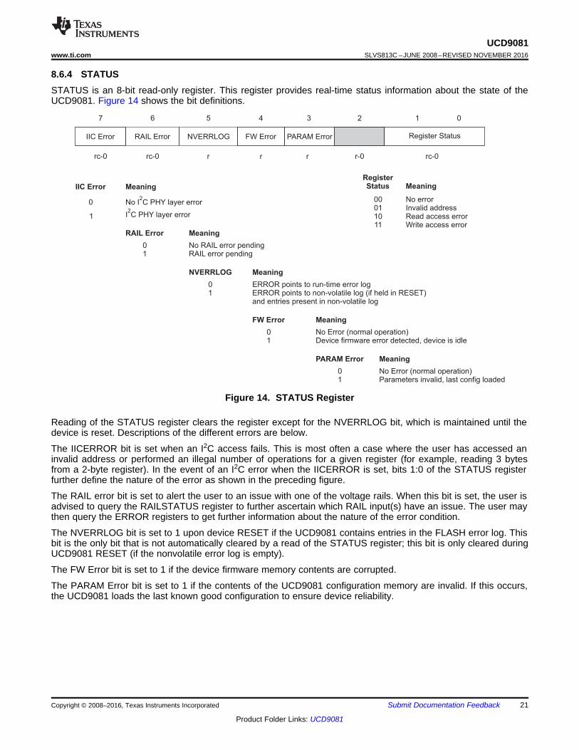
8.6.4 STATUSSTATUS is an 8-bit read-only register. This register provides real-time status information about the state of theUCD9081. Figure 14 shows the bit definitions.
Figure 14. STATUS Register
Reading of the STATUS register clears the register except for the NVERRLOG bit, which is maintained until thedevice is reset. Descriptions of the different errors are below.
The IICERROR bit is set when an I2C access fails. This is most often a case where the user has accessed aninvalid address or performed an illegal number of operations for a given register (for example, reading 3 bytesfrom a 2-byte register). In the event of an I2C error when the IICERROR is set, bits 1:0 of the STATUS registerfurther define the nature of the error as shown in the preceding figure.
The RAIL error bit is set to alert the user to an issue with one of the voltage rails. When this bit is set, the user isadvised to query the RAILSTATUS register to further ascertain which RAIL input(s) have an issue. The user maythen query the ERROR registers to get further information about the nature of the error condition.
The NVERRLOG bit is set to 1 upon device RESET if the UCD9081 contains entries in the FLASH error log. Thisbit is the only bit that is not automatically cleared by a read of the STATUS register; this bit is only cleared duringUCD9081 RESET (if the nonvolatile error log is empty).
The FW Error bit is set to 1 if the device firmware memory contents are corrupted.
The PARAM Error bit is set to 1 if the contents of the UCD9081 configuration memory are invalid. If this occurs,the UCD9081 loads the last known good configuration to ensure device reliability.
FLASHLOCK
7 6 5 4 3 2 1 0
rw-0 rw-0 rw-0 rw-0 rw-0 rw-0 rw-0 rw-0
FLASHLOCK
0x00 Lock flash (default)
0x01 Flash is being updated
0x02 Unlock flash (before configuration)
1415 13 12 11 10 9 8 7 6 5 4 3 2 1 0
rc-0 rc-0 rc-0 rc-0 rc-0 rc-0 rc-0 rc-0
RAIL8
rc-0 rc-0 rc-0 rc-0 rc-0 rc-0 rc-0rc-0
RAIL7 RAIL6 RAIL5 RAIL4 RAIL3 RAIL2 RAIL1
RAILn Meaning0 No alarm pending for R n1 Alarm pending for RAILn
AIL
Minor
7 6 5 4 3 2 1 0
r r r r r r r r
Major
22
UCD9081SLVS813C –JUNE 2008–REVISED NOVEMBER 2016 www.ti.com
Product Folder Links: UCD9081
Submit Documentation Feedback Copyright © 2008–2016, Texas Instruments Incorporated
8.6.5 VERSIONThe VERSION register provides the user with access to the device revision of the UCD9081. The format of thisregister is a nibble-based major/minor format as shown in Figure 15.
Figure 15. VERSION Major/Minor Register
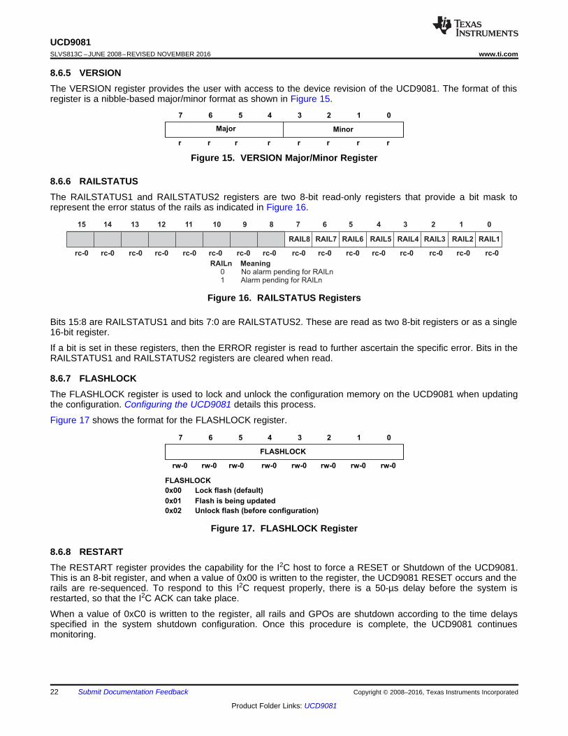
8.6.6 RAILSTATUSThe RAILSTATUS1 and RAILSTATUS2 registers are two 8-bit read-only registers that provide a bit mask torepresent the error status of the rails as indicated in Figure 16.
Figure 16. RAILSTATUS Registers
Bits 15:8 are RAILSTATUS1 and bits 7:0 are RAILSTATUS2. These are read as two 8-bit registers or as a single16-bit register.
If a bit is set in these registers, then the ERROR register is read to further ascertain the specific error. Bits in theRAILSTATUS1 and RAILSTATUS2 registers are cleared when read.
8.6.7 FLASHLOCKThe FLASHLOCK register is used to lock and unlock the configuration memory on the UCD9081 when updatingthe configuration. Configuring the UCD9081 details this process.
Figure 17 shows the format for the FLASHLOCK register.
Figure 17. FLASHLOCK Register
8.6.8 RESTARTThe RESTART register provides the capability for the I2C host to force a RESET or Shutdown of the UCD9081.This is an 8-bit register, and when a value of 0x00 is written to the register, the UCD9081 RESET occurs and therails are re-sequenced. To respond to this I2C request properly, there is a 50-µs delay before the system isrestarted, so that the I2C ACK can take place.
When a value of 0xC0 is written to the register, all rails and GPOs are shutdown according to the time delaysspecified in the system shutdown configuration. Once this procedure is complete, the UCD9081 continuesmonitoring.
Data
rw
07815
WDATA2
(0x33)
WDATA1
(0x32)
rw
Address
07815
rw-0x00 rw-0x00
WADDR2
(0x31)
WADDR1
(0x30)
23
UCD9081www.ti.com SLVS813C –JUNE 2008–REVISED NOVEMBER 2016
Product Folder Links: UCD9081
Submit Documentation FeedbackCopyright © 2008–2016, Texas Instruments Incorporated
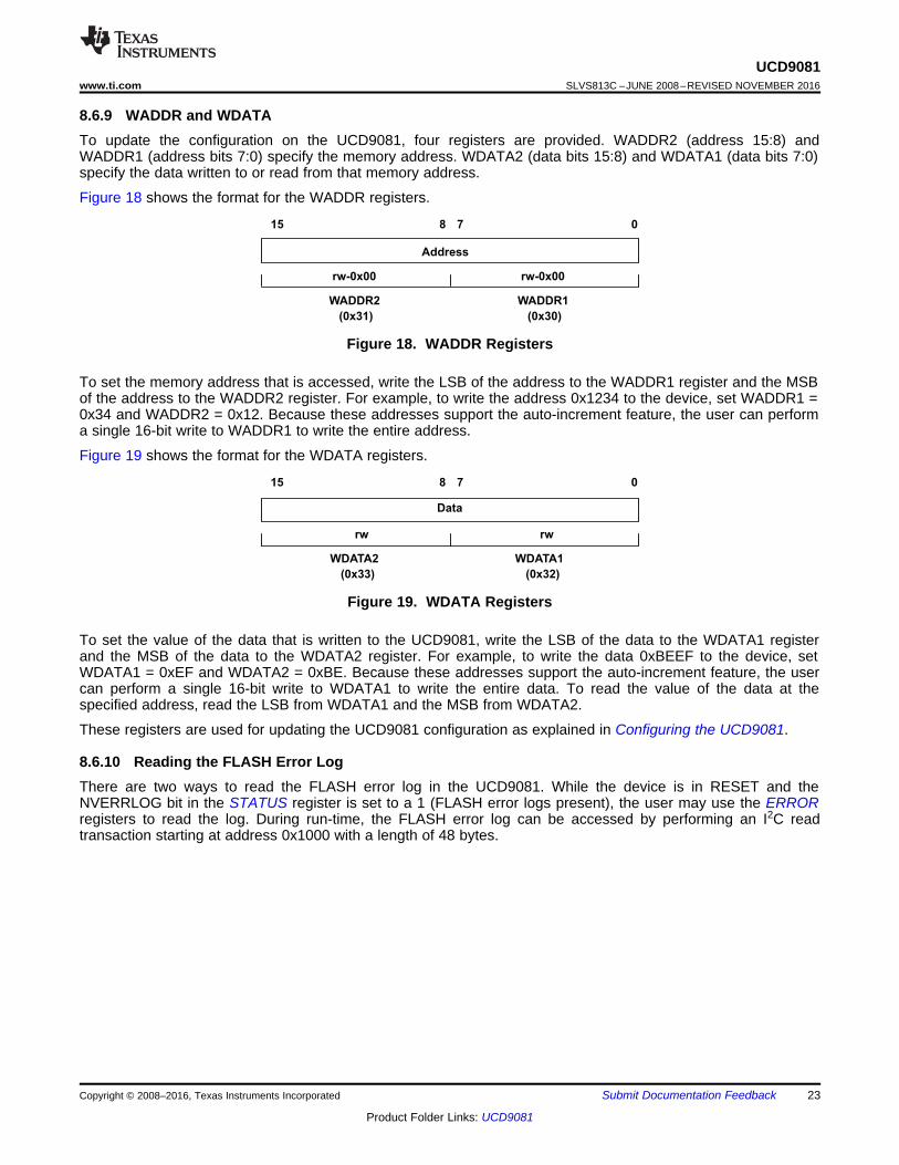
8.6.9 WADDR and WDATATo update the configuration on the UCD9081, four registers are provided. WADDR2 (address 15:8) andWADDR1 (address bits 7:0) specify the memory address. WDATA2 (data bits 15:8) and WDATA1 (data bits 7:0)specify the data written to or read from that memory address.
Figure 18 shows the format for the WADDR registers.
Figure 18. WADDR Registers
To set the memory address that is accessed, write the LSB of the address to the WADDR1 register and the MSBof the address to the WADDR2 register. For example, to write the address 0x1234 to the device, set WADDR1 =0x34 and WADDR2 = 0x12. Because these addresses support the auto-increment feature, the user can performa single 16-bit write to WADDR1 to write the entire address.
Figure 19 shows the format for the WDATA registers.
Figure 19. WDATA Registers
To set the value of the data that is written to the UCD9081, write the LSB of the data to the WDATA1 registerand the MSB of the data to the WDATA2 register. For example, to write the data 0xBEEF to the device, setWDATA1 = 0xEF and WDATA2 = 0xBE. Because these addresses support the auto-increment feature, the usercan perform a single 16-bit write to WDATA1 to write the entire data. To read the value of the data at thespecified address, read the LSB from WDATA1 and the MSB from WDATA2.
These registers are used for updating the UCD9081 configuration as explained in Configuring the UCD9081.
8.6.10 Reading the FLASH Error LogThere are two ways to read the FLASH error log in the UCD9081. While the device is in RESET and theNVERRLOG bit in the STATUS register is set to a 1 (FLASH error logs present), the user may use the ERRORregisters to read the log. During run-time, the FLASH error log can be accessed by performing an I2C readtransaction starting at address 0x1000 with a length of 48 bytes.
24
UCD9081SLVS813C –JUNE 2008–REVISED NOVEMBER 2016 www.ti.com
Product Folder Links: UCD9081
Submit Documentation Feedback Copyright © 2008–2016, Texas Instruments Incorporated
9 Application and Implementation
NOTEInformation in the following applications sections is not part of the TI componentspecification, and TI does not warrant its accuracy or completeness. TI’s customers areresponsible for determining suitability of components for their purposes. Customers shouldvalidate and test their design implementation to confirm system functionality.
9.1 Application Information
9.1.1 Considerations for MONX Input Series Resistance, RS
RS is the series impedance between the sampled voltage source (low impedance power supply output) and theUCD9081 MONx input pin. This resistance can affect UCD9081 sampling accuracy if it is too large. In mostcases (when the power supply being monitored has a lower VOUT than the UCD9081 voltage reference beingused) this resistance is low and can be ignored. In cases where a voltage divider is used to scale the monitoredvoltage below the voltage reference, the impedance of this network must be chosen so that it does not adverselyaffect the analog to digital converter (ADC) conversion accuracy. The equivalent series impedance (RS) of thedivider network is just the parallel combination of the pullup and pulldown resistors.
The UCD9081 has an internal clock (DCO) whose frequency is set by ROSC on pin 32. The DCO frequency canbe affected by several factors including supply voltage and temperature. This clock is used by the ADC to set upan ADC sample or gate time (TGATE) at each MONx pin. The voltage sampled must be allowed to settlesufficiently during TGATE. The settling time is affected by the UCD9081 internal capacitance and RS. To allow forsufficient settling time over DCO frequency, supply voltage, and temperature variation, choose RS < 6 kΩ.
9.1.2 Estimating UCD9081 Reporting Accuracy Over Variations in ADC Voltage ReferenceThe UCD9081 uses a 10-bit ADC. The ADC in the UCD9081 derives its reference voltage (VR+ ) from either theexternal (VCC pin) or internal (VREF+) reference voltage to scale the digitally reported voltage. The least significantbit (LSB) voltage value is VLSB = VR+/2n where n = 10 and VR+ is the reference voltage used (either external VCC= 3.3 V nominal, or internal VREF+ = 2.5 V nominal). For external VR+ = VCC = 3.3 V, VLSB = 3.3 / 1024 = 3.22 mVand for internal VR+ = VREF+ = 2.5 V, VLSB = 2.5 / 1024 = 2.44 mV.
The error in the reported voltage is a function of the ADC linearity error(s) as well as variations in the ADCreference voltage. The total unadjusted error (ETUE) for the ADC in the UCD9081 is ±5 LSB and the variation ofthe internal 2.5-V reference is ±6% maximum. VTUE is calculated as VLSB × ETUE for the particular referencevoltage used. The reported voltage error is the sum of the reference voltage error and the ADC total unadjustederror. At lower monitored voltages, ETUE may dominate reported error while at higher monitored voltages VR+dominates the reported error. Reported error (percent) can be calculated using Equation 3.
RPTERR = [(1 + REFTOL) / VACT] × [VR+ × ETUE / 1024 + VACT] – 1
where• REFTOL is VR+ tolerance• VACT is actual voltage monitored (at the UCD9081 MONx pin)• VR+ is the nominal voltage of the ADC reference (3)
Listed below are four examples using Equation 3 to estimate reported error:• VR+ = 2.5 V, REFTOL = 6%, VACT = 0.25 V, RPTERR = 11.2%• VR+ = 2.5 V, REFTOL = 6%, VACT = 2.25 V, RPTERR = 6.6%• VR+ = 3.3 V, REFTOL = 1%, VACT = 0.25 V, RPTERR = 7.5%• VR+ = 3.3 V, REFTOL = 1%, VACT = 2.25 V, RPTERR = 1.7%
In addition to the reporting errors due to ADC and voltage reference, there can be additional errors due to dividerresistor tolerance when monitoring voltages higher than VR+. These errors can be added to the reporting errordescribed above.
25
UCD9081www.ti.com SLVS813C –JUNE 2008–REVISED NOVEMBER 2016
Product Folder Links: UCD9081
Submit Documentation FeedbackCopyright © 2008–2016, Texas Instruments Incorporated
9.2 Typical ApplicationFigure 20 illustrates a typical power supply sequencing configuration. Power Supply 1 and Power Supply Xrequire active low enables while Power Supply 2 and Power Supply 3 require active high enables. VOUT1 andVOUT3 exceed the selected A/D reference voltage so their outputs are divided before being sampled by the MON1and MON3 inputs. VOUT2 and VOUTX are within the selected A/D reference voltage so their outputs can besampled directly by the MON2 and MON7 inputs. Figure 20 illustrates the use of the GPO digital output pins toprovide status and power on reset to other system devices.
UCD9081
23
24
11
10
12
13
14
EN1
EN2
EN3
EN4
EN5
EN6
EN7
21
22
1SDA
SCL
6
7
8
18
19
9
15
30VCC
VSS
MON1
MON2
MON3
MON4
MON5
MON6
MON7
26 25
10kW
10kW
EN
EN
EN
3.3V
3.3V
3.3V
16 MON8
28 27
2
17
NC
NC
32
5
ROSC
RST
3 XIN
29 TEST 20
31
NC
NC4 NC
10kW
100kW
3.3V
3.3V 3.3V
0.01 Fm3.3V
3.3V
3.3V
DNP
10kW
3.3V
1kW
10kW
3.3V
DNP
10kW
3.3V
1kW
10kW
POR1
3.3V
POR2
POR3
POR4
*
*
*
EX: Slave I C Address = 0x65(Internal ADDR[7:5] = 0b110)
2
I CMaster
2
3.3VRegulator
V
RTNBUS
VBUS
1 Fm
SystemDeviceResets
VOUT1
VOUT2
VOUT3
PowerSupply
1
PowerSupply
2
PowerSupply
3
EN
VOUTXPowerSupply
X
EN8/ADDR1/G PO1
ADDR3/G PO3
ADDR2/G PO2
ADDR4/G PO4
330W
StatusLEDs
Copyright © 2016, Texas Instruments Incorporated
UCD9081SLVS813C –JUNE 2008–REVISED NOVEMBER 2016 www.ti.com
26
Product Folder Links: UCD9081
Submit Documentation Feedback Copyright © 2008–2016, Texas Instruments Incorporated
Figure 20. Typical Power Supply Sequencing Application
27
UCD9081www.ti.com SLVS813C –JUNE 2008–REVISED NOVEMBER 2016
Product Folder Links: UCD9081
Submit Documentation FeedbackCopyright © 2008–2016, Texas Instruments Incorporated
9.2.1 Design RequirementsRST pin must have a 10-kΩ pullup resistor to 3.3 V and 10-nF decoupling capacitor to ground. The componentmust be placed as close to the RST pin as possible.
9.2.2 Detailed Design ProcedureUCD9081 GUI can be used to design the device configuration. An USB-to-I2C Adapter from Texas Instrumentscan be used to connect GUI to I2C.
General design steps include:1. General rail setup2. Rail sequencing conditions setup3. Alarm action (fault response) setup4. System conditions setup5. General GPO setup6. GPO sequence setup
After configuration changes, click Store to Buffer to save the current entries to a GUI. Click Update Parametersand Sequence to permanently store the new configuration into the device data flash.
9.2.3 Application Curve
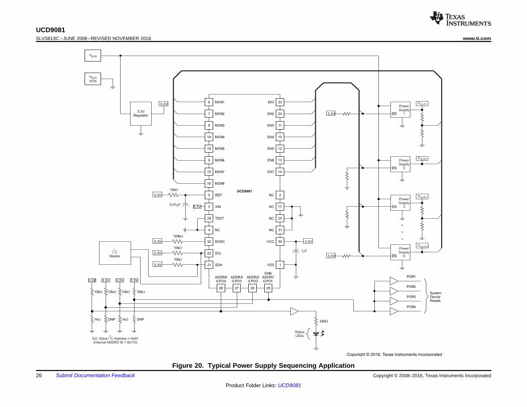
Figure 21. Example Power-On Sequence
Power Pad Connected to VSS
[
[
PIN2 Not
Connected [[
PIN4 Connected
To VSS
[
[PIN20 Connected
To VSS
[
[
PIN17 Connected
To VSS
[
[
PIN
31
Co
nn
ecte
d
To
VS
S
28
UCD9081SLVS813C –JUNE 2008–REVISED NOVEMBER 2016 www.ti.com
Product Folder Links: UCD9081
Submit Documentation Feedback Copyright © 2008–2016, Texas Instruments Incorporated
10 Power Supply RecommendationsUse a 3.3-V power supply with the UCD9081.
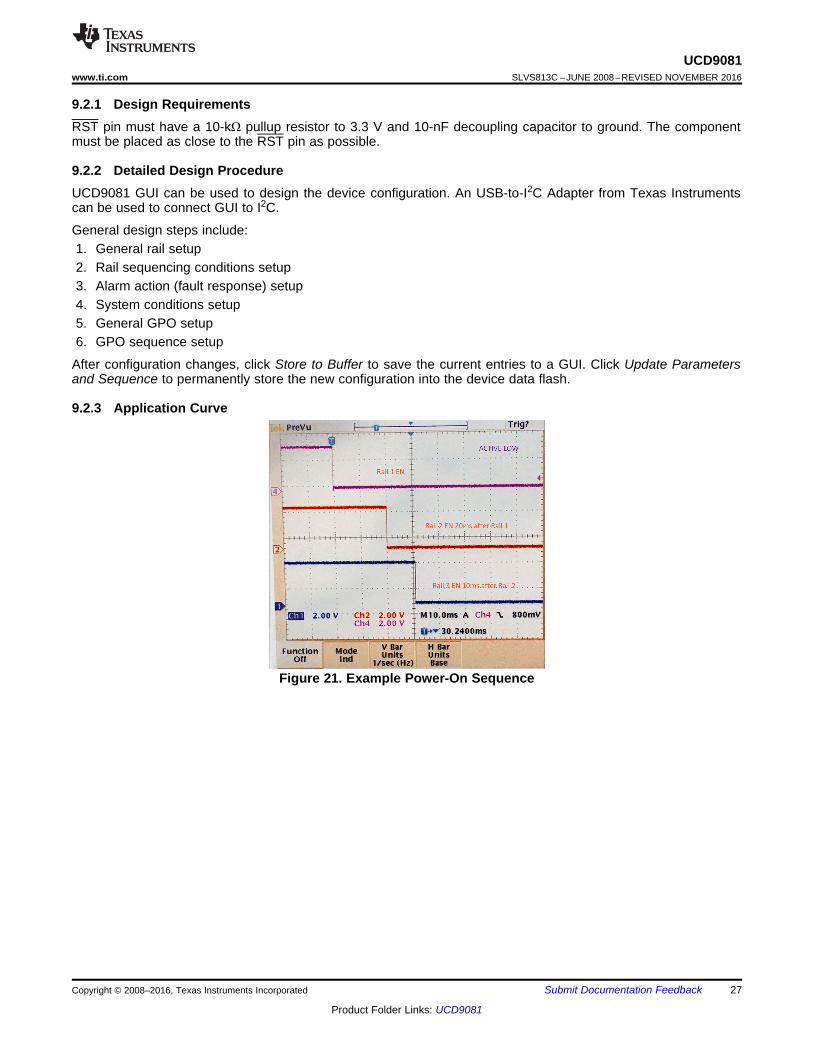
11 Layout
11.1 Layout GuidelinesThe power pad provides a thermal and mechanical interface between the device and the printed-circuit board(PCB). Connect the power pad to the device VSS pins. Pin 2 must not be connected. Pin (4, 17, 20, 31) arerecommended to connect to VSS because these pins are not connected internally.
11.2 Layout Example
Figure 22. UCD9081 Layout, Top Layer
29
UCD9081www.ti.com SLVS813C –JUNE 2008–REVISED NOVEMBER 2016
Product Folder Links: UCD9081
Submit Documentation FeedbackCopyright © 2008–2016, Texas Instruments Incorporated
12 Device and Documentation Support
12.1 Documentation Support
12.1.1 Related DocumentationFor related documentation see the following:• UCD9081 EVM User's Guide (SLVU249)• UCD9081 Programming Guide (SLVA275)
12.2 Receiving Notification of Documentation UpdatesTo receive notification of documentation updates, navigate to the device product folder on ti.com. In the upperright corner, click on Alert me to register and receive a weekly digest of any product information that haschanged. For change details, review the revision history included in any revised document.
12.3 Community ResourcesThe following links connect to TI community resources. Linked contents are provided "AS IS" by the respectivecontributors. They do not constitute TI specifications and do not necessarily reflect TI's views; see TI's Terms ofUse.
TI E2E™ Online Community TI's Engineer-to-Engineer (E2E) Community. Created to foster collaborationamong engineers. At e2e.ti.com, you can ask questions, share knowledge, explore ideas and helpsolve problems with fellow engineers.
Design Support TI's Design Support Quickly find helpful E2E forums along with design support tools andcontact information for technical support.
12.4 TrademarksPowerPAD, TMS320, E2E are trademarks of Texas Instruments.Windows is a trademark of Microsoft Corporation.I2C is a trademark of Phillips Electronics.All other trademarks are the property of their respective owners.
12.5 Electrostatic Discharge CautionThese devices have limited built-in ESD protection. The leads should be shorted together or the device placed in conductive foamduring storage or handling to prevent electrostatic damage to the MOS gates.
12.6 GlossarySLYZ022 — TI Glossary.
This glossary lists and explains terms, acronyms, and definitions.
13 Mechanical, Packaging, and Orderable InformationThe following pages include mechanical, packaging, and orderable information. This information is the mostcurrent data available for the designated devices. This data is subject to change without notice and revision ofthis document. For browser-based versions of this data sheet, refer to the left-hand navigation.
PACKAGE OPTION ADDENDUM
www.ti.com 16-Mar-2016
Addendum-Page 1
PACKAGING INFORMATION
Orderable Device Status(1)
Package Type PackageDrawing
Pins PackageQty
Eco Plan(2)
Lead/Ball Finish(6)
MSL Peak Temp(3)
Op Temp (°C) Device Marking(4/5)
Samples
UCD9081RHBR ACTIVE VQFN RHB 32 3000 Green (RoHS& no Sb/Br)
CU NIPDAU Level-2-260C-1 YEAR -40 to 85 UCD9081
UCD9081RHBRG4 ACTIVE VQFN RHB 32 3000 Green (RoHS& no Sb/Br)
CU NIPDAU Level-2-260C-1 YEAR -40 to 85 UCD9081
UCD9081RHBT ACTIVE VQFN RHB 32 250 Green (RoHS& no Sb/Br)
CU NIPDAU Level-2-260C-1 YEAR -40 to 85 UCD9081
UCD9081RHBTG4 ACTIVE VQFN RHB 32 250 Green (RoHS& no Sb/Br)
CU NIPDAU Level-2-260C-1 YEAR -40 to 85 UCD9081
(1) The marketing status values are defined as follows:ACTIVE: Product device recommended for new designs.LIFEBUY: TI has announced that the device will be discontinued, and a lifetime-buy period is in effect.NRND: Not recommended for new designs. Device is in production to support existing customers, but TI does not recommend using this part in a new design.PREVIEW: Device has been announced but is not in production. Samples may or may not be available.OBSOLETE: TI has discontinued the production of the device.
(2) Eco Plan - The planned eco-friendly classification: Pb-Free (RoHS), Pb-Free (RoHS Exempt), or Green (RoHS & no Sb/Br) - please check http://www.ti.com/productcontent for the latest availabilityinformation and additional product content details.TBD: The Pb-Free/Green conversion plan has not been defined.Pb-Free (RoHS): TI's terms "Lead-Free" or "Pb-Free" mean semiconductor products that are compatible with the current RoHS requirements for all 6 substances, including the requirement thatlead not exceed 0.1% by weight in homogeneous materials. Where designed to be soldered at high temperatures, TI Pb-Free products are suitable for use in specified lead-free processes.Pb-Free (RoHS Exempt): This component has a RoHS exemption for either 1) lead-based flip-chip solder bumps used between the die and package, or 2) lead-based die adhesive used betweenthe die and leadframe. The component is otherwise considered Pb-Free (RoHS compatible) as defined above.Green (RoHS & no Sb/Br): TI defines "Green" to mean Pb-Free (RoHS compatible), and free of Bromine (Br) and Antimony (Sb) based flame retardants (Br or Sb do not exceed 0.1% by weightin homogeneous material)
(3) MSL, Peak Temp. - The Moisture Sensitivity Level rating according to the JEDEC industry standard classifications, and peak solder temperature.
(4) There may be additional marking, which relates to the logo, the lot trace code information, or the environmental category on the device.
(5) Multiple Device Markings will be inside parentheses. Only one Device Marking contained in parentheses and separated by a "~" will appear on a device. If a line is indented then it is a continuationof the previous line and the two combined represent the entire Device Marking for that device.
(6) Lead/Ball Finish - Orderable Devices may have multiple material finish options. Finish options are separated by a vertical ruled line. Lead/Ball Finish values may wrap to two lines if the finishvalue exceeds the maximum column width.
PACKAGE OPTION ADDENDUM
www.ti.com 16-Mar-2016
Addendum-Page 2
Important Information and Disclaimer:The information provided on this page represents TI's knowledge and belief as of the date that it is provided. TI bases its knowledge and belief on informationprovided by third parties, and makes no representation or warranty as to the accuracy of such information. Efforts are underway to better integrate information from third parties. TI has taken andcontinues to take reasonable steps to provide representative and accurate information but may not have conducted destructive testing or chemical analysis on incoming materials and chemicals.TI and TI suppliers consider certain information to be proprietary, and thus CAS numbers and other limited information may not be available for release.
In no event shall TI's liability arising out of such information exceed the total purchase price of the TI part(s) at issue in this document sold by TI to Customer on an annual basis.
TAPE AND REEL INFORMATION
*All dimensions are nominal
Device PackageType
PackageDrawing
Pins SPQ ReelDiameter
(mm)
ReelWidth
W1 (mm)
A0(mm)
B0(mm)
K0(mm)
P1(mm)
W(mm)
Pin1Quadrant
UCD9081RHBR VQFN RHB 32 3000 330.0 12.4 5.3 5.3 1.5 8.0 12.0 Q2
UCD9081RHBT VQFN RHB 32 250 180.0 12.4 5.3 5.3 1.5 8.0 12.0 Q2
PACKAGE MATERIALS INFORMATION
www.ti.com 16-Mar-2016
Pack Materials-Page 1
*All dimensions are nominal
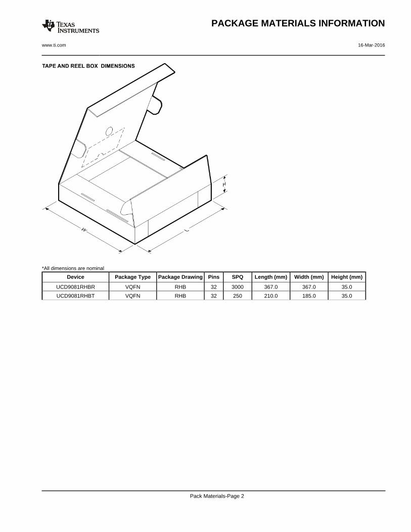
Device Package Type Package Drawing Pins SPQ Length (mm) Width (mm) Height (mm)
UCD9081RHBR VQFN RHB 32 3000 367.0 367.0 35.0
UCD9081RHBT VQFN RHB 32 250 210.0 185.0 35.0
PACKAGE MATERIALS INFORMATION
www.ti.com 16-Mar-2016
Pack Materials-Page 2

IMPORTANT NOTICE
Texas Instruments Incorporated and its subsidiaries (TI) reserve the right to make corrections, enhancements, improvements and otherchanges to its semiconductor products and services per JESD46, latest issue, and to discontinue any product or service per JESD48, latestissue. Buyers should obtain the latest relevant information before placing orders and should verify that such information is current andcomplete. All semiconductor products (also referred to herein as “components”) are sold subject to TI’s terms and conditions of salesupplied at the time of order acknowledgment.TI warrants performance of its components to the specifications applicable at the time of sale, in accordance with the warranty in TI’s termsand conditions of sale of semiconductor products. Testing and other quality control techniques are used to the extent TI deems necessaryto support this warranty. Except where mandated by applicable law, testing of all parameters of each component is not necessarilyperformed.TI assumes no liability for applications assistance or the design of Buyers’ products. Buyers are responsible for their products andapplications using TI components. To minimize the risks associated with Buyers’ products and applications, Buyers should provideadequate design and operating safeguards.TI does not warrant or represent that any license, either express or implied, is granted under any patent right, copyright, mask work right, orother intellectual property right relating to any combination, machine, or process in which TI components or services are used. Informationpublished by TI regarding third-party products or services does not constitute a license to use such products or services or a warranty orendorsement thereof. Use of such information may require a license from a third party under the patents or other intellectual property of thethird party, or a license from TI under the patents or other intellectual property of TI.Reproduction of significant portions of TI information in TI data books or data sheets is permissible only if reproduction is without alterationand is accompanied by all associated warranties, conditions, limitations, and notices. TI is not responsible or liable for such altereddocumentation. Information of third parties may be subject to additional restrictions.Resale of TI components or services with statements different from or beyond the parameters stated by TI for that component or servicevoids all express and any implied warranties for the associated TI component or service and is an unfair and deceptive business practice.TI is not responsible or liable for any such statements.Buyer acknowledges and agrees that it is solely responsible for compliance with all legal, regulatory and safety-related requirementsconcerning its products, and any use of TI components in its applications, notwithstanding any applications-related information or supportthat may be provided by TI. Buyer represents and agrees that it has all the necessary expertise to create and implement safeguards whichanticipate dangerous consequences of failures, monitor failures and their consequences, lessen the likelihood of failures that might causeharm and take appropriate remedial actions. Buyer will fully indemnify TI and its representatives against any damages arising out of the useof any TI components in safety-critical applications.In some cases, TI components may be promoted specifically to facilitate safety-related applications. With such components, TI’s goal is tohelp enable customers to design and create their own end-product solutions that meet applicable functional safety standards andrequirements. Nonetheless, such components are subject to these terms.No TI components are authorized for use in FDA Class III (or similar life-critical medical equipment) unless authorized officers of the partieshave executed a special agreement specifically governing such use.Only those TI components which TI has specifically designated as military grade or “enhanced plastic” are designed and intended for use inmilitary/aerospace applications or environments. Buyer acknowledges and agrees that any military or aerospace use of TI componentswhich have not been so designated is solely at the Buyer's risk, and that Buyer is solely responsible for compliance with all legal andregulatory requirements in connection with such use.TI has specifically designated certain components as meeting ISO/TS16949 requirements, mainly for automotive use. In any case of use ofnon-designated products, TI will not be responsible for any failure to meet ISO/TS16949.
Products ApplicationsAudio www.ti.com/audio Automotive and Transportation www.ti.com/automotiveAmplifiers amplifier.ti.com Communications and Telecom www.ti.com/communicationsData Converters dataconverter.ti.com Computers and Peripherals www.ti.com/computersDLP® Products www.dlp.com Consumer Electronics www.ti.com/consumer-appsDSP dsp.ti.com Energy and Lighting www.ti.com/energyClocks and Timers www.ti.com/clocks Industrial www.ti.com/industrialInterface interface.ti.com Medical www.ti.com/medicalLogic logic.ti.com Security www.ti.com/securityPower Mgmt power.ti.com Space, Avionics and Defense www.ti.com/space-avionics-defenseMicrocontrollers microcontroller.ti.com Video and Imaging www.ti.com/videoRFID www.ti-rfid.comOMAP Applications Processors www.ti.com/omap TI E2E Community e2e.ti.comWireless Connectivity www.ti.com/wirelessconnectivity
Mailing Address: Texas Instruments, Post Office Box 655303, Dallas, Texas 75265Copyright © 2016, Texas Instruments Incorporated