(760) 744-0300 sales@hughescircuits · powerpoint presentation author: todd anderson created date:...
TRANSCRIPT

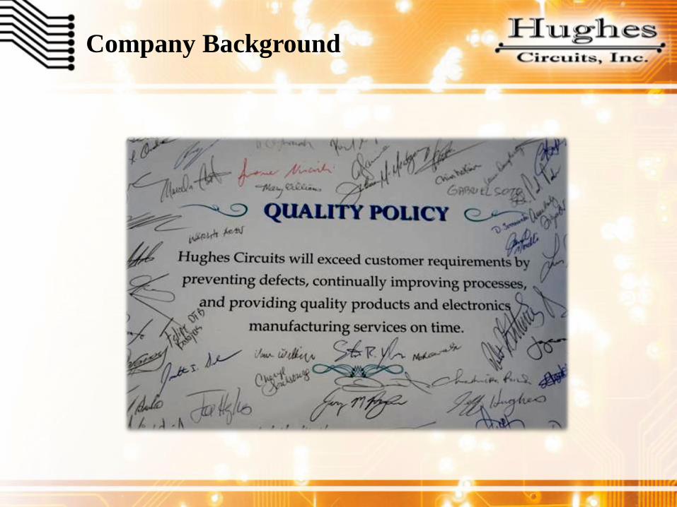
Company Background
A Performance-oriented Legacy Founded in 1999 by Jerry Hughes
• 47 years in the circuit board business, founding 2 successful prototype PCB companies • Spearheaded and implemented in-house prototype facilities within Burroughs, NCR and Unisys • The underlying theme of the company – strong front-end and engineering support • Keen understanding of time sensitive products and constraints
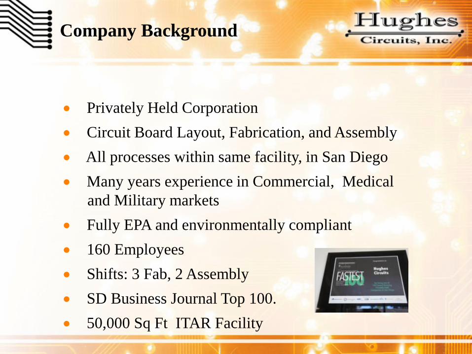
Company Background
• Privately Held Corporation • Circuit Board Layout, Fabrication, and Assembly • All processes within same facility, in San Diego • Many years experience in Commercial, Medical and Military markets • Fully EPA and environmentally compliant • 160 Employees • Shifts: 3 Fab, 2 Assembly • SD Business Journal Top 100. • 50,000 Sq Ft ITAR Facility

Company Background
• CAGE 1KXU6 • Active in Trade Shows • Growing 15%+ Yr/Yr • Operating at 65% Capacity • Recent Capital Investments
• Additional LDI • Additional LASER •. Additional AOI

Company Background MIL/AERO 65% L3 Communications Boeing General Atomics Raytheon Northrop Grumman ( Supplier of the Year) Aethercomm MEDICAL 20% Boston Scientific Sparton Medical Medtronic Illumina COMMERCIAL/IND 15% Universal Electronics Delta Design Microprobe SRAM PANAVISION These are to name a few of our satisfied customers. References available upon request
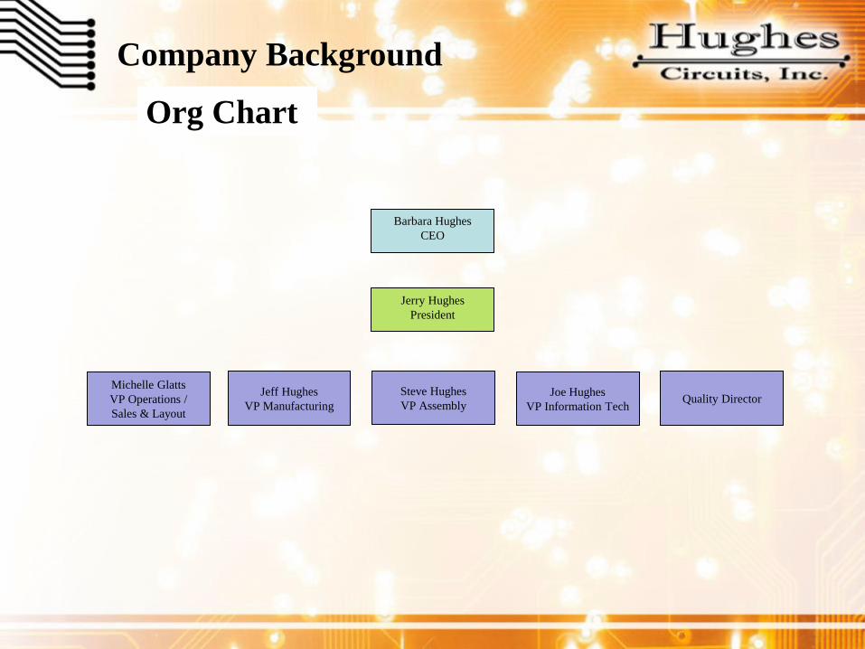
Company Background
Org Chart
Barbara Hughes CEO
Jerry Hughes President
Jeff Hughes VP Manufacturing
Joe Hughes VP Information Tech
Steve Hughes VP Assembly
Michelle Glatts VP Operations / Sales & Layout
Quality Director
Company Background
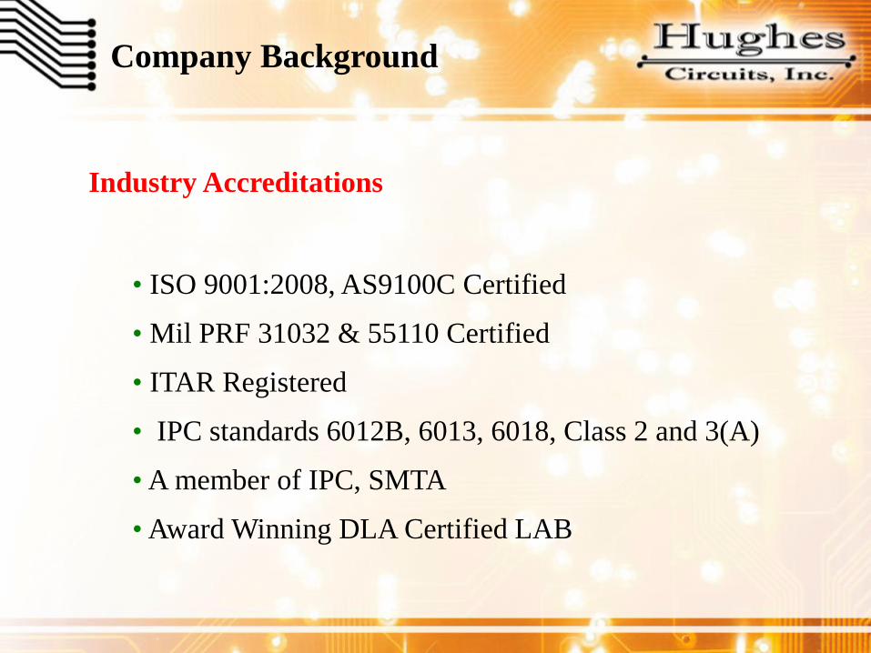
• ISO 9001:2008, AS9100C Certified
• Mil PRF 31032 & 55110 Certified
• ITAR Registered
• IPC standards 6012B, 6013, 6018, Class 2 and 3(A)
• A member of IPC, SMTA
• Award Winning DLA Certified LAB
Industry Accreditations
Company Background

Your Layout Partner
Hughes Teams with your Board Layout Designers A Performance-oriented Resource Partner:
• Gives you one source Layout/build • Controlled outsourcing • One point of contact for complete process
Featuring: • Both original board Layout and repackaging • Experienced, Senior Layout Engineers • Hundreds of satisfied clients
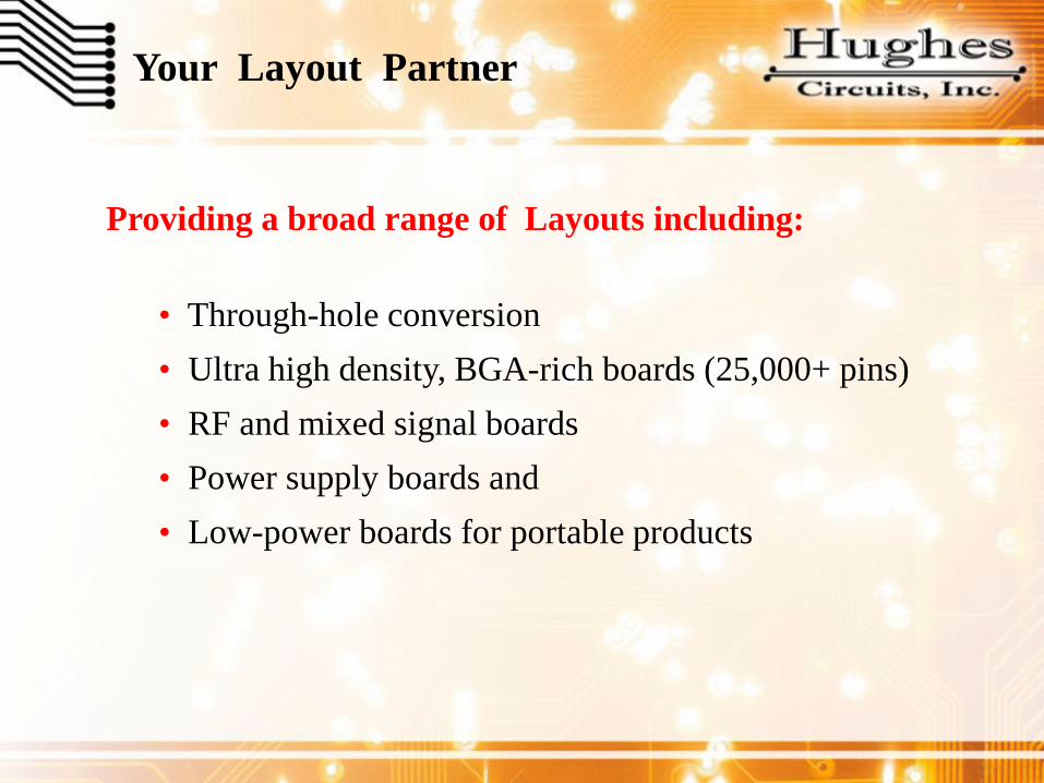
Your Layout Partner
Providing a broad range of Layouts including:
• Through-hole conversion • Ultra high density, BGA-rich boards (25,000+ pins) • RF and mixed signal boards • Power supply boards and • Low-power boards for portable products
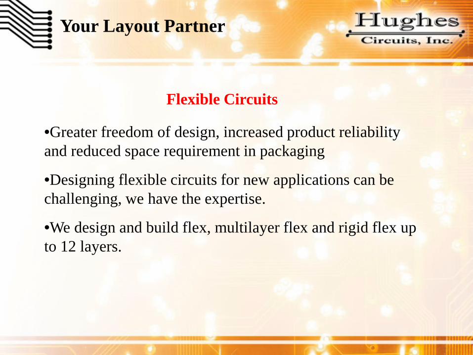
•Greater freedom of design, increased product reliability and reduced space requirement in packaging
•Designing flexible circuits for new applications can be challenging, we have the expertise.
•We design and build flex, multilayer flex and rigid flex up to 12 layers.
Flexible Circuits
Your Layout Partner

Your Layout Partner
Talent and Tools Experience :
• Several Full-Time Layout Engineers, average over 20 years of PCB layout experience with wide variety of designs • All are IPC Certified Interconnect Designers (CID)
Tools: • Cadence Allegro, Mentor PADS, Altium Designer, Orcad, DxDesigner • Valor GenFlex, Polar and PCB Libraries
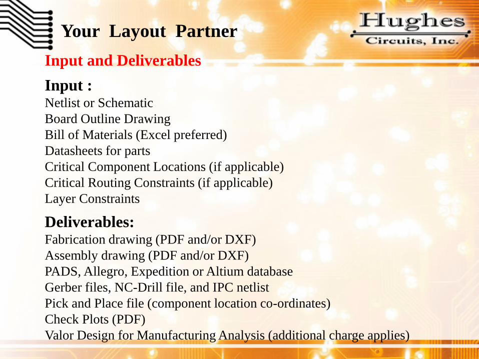
Your Layout Partner Input and Deliverables Input : Netlist or Schematic Board Outline Drawing Bill of Materials (Excel preferred) Datasheets for parts Critical Component Locations (if applicable) Critical Routing Constraints (if applicable) Layer Constraints
Deliverables: Fabrication drawing (PDF and/or DXF) Assembly drawing (PDF and/or DXF) PADS, Allegro, Expedition or Altium database Gerber files, NC-Drill file, and IPC netlist Pick and Place file (component location co-ordinates) Check Plots (PDF) Valor Design for Manufacturing Analysis (additional charge applies)

General Manufacturing Capabilities
• RF Boards • Rogers, Taconic, Arlon Nelco
• FR4 •Isola, Nelco, Getek
• Polyimide •Isola, Nelco, Arlon
• Flex •Dupont, Panasonic
• Metal Backed Fabrication •Aluminum, Copper, Brass
• 1-50+ layers • 10 to 1 Mech Drill aspect ratio • 1 to 1 laser via • Reverse Pulse Plating • 100% Netlist testing • Controlled Impedance –TDR • Controlled dielectrics
Fabrication Materials
Fabrication Capabilities
General Manufacturing Capabilities
Technologies
• Controlled depth drill, laser blind vias
• Burr free plated edges and half-holes • Multilevel “Cavity” Boards • Blind and Buried vias • via-in-pad, conductive filled holes • Conductors and spaces down to 2 mils • Multilayer thickness from .015” to .325” • Buried Resistance and Capacitance • Metal Backed Boards, Aluminum, Copper etc.
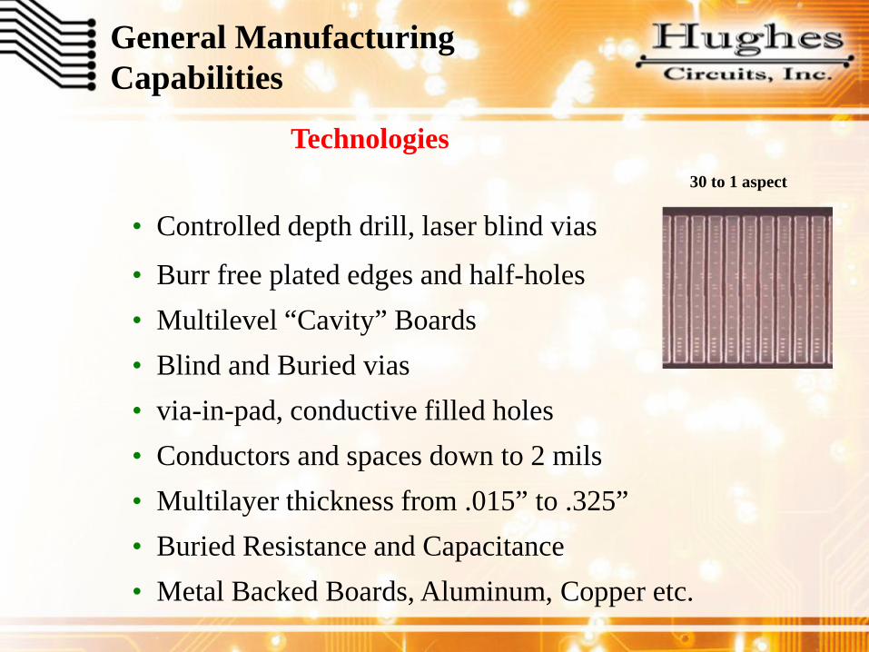
30 to 1 aspect
General Manufacturing Capabilities
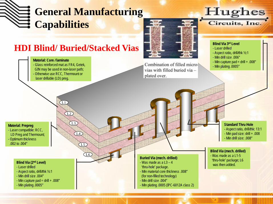
HDI Blind/ Buried/Stacked Vias
Blind Via (mech. drilled) - Was made as a L1-5 ‘thru-hole’ package; L6 was then added.
Buried Via (mech. drilled) - Was made as a L3 – 4 ‘thru-hole’ package. - Min material core thickness .008” (for non-filled technology) - Min drill size .004” - Min plating .0005 (IPC-6012A class 2)
Blind Via (2nd Level) - Laser drilled - Aspect ratio, drill/thk ½:1 - Min drill size .004” - Min capture pad = drill + .008” - Min plating .0005”
Material: Prepreg - Laser compatible: RCC, LD Preg and Thermount; - Optimum thickness .002 to .004”
Material: Core / laminate - Glass reinforced mat as FR4, Getek, GIN may be used in non-laser path; - Otherwise use RCC, Thermount or laser drillable (LD) preg.
Blind Via 3rd Level - Laser drilled - Aspect ratio, drill/thk ½:1 - Min drill size .006” - Min capture pad = drill + .008” - Min plating .0005”
Standard Thru Hole - Aspect ratio, drill/thk: 13:1 - Min pad size: drill + .008 - Min drill size: .008”
L2
L1
L3
L4
L5
L6
General Manufacturing Capabilities
Board Finishes
• LPI/LDI (liquid photo imageable) solder mask and silk screen
•TAIYO • Entek / OSP • Carbon ink
Plating Finishes Available
• HASL (hot air level) • Lead Free HASL* • ENIG • ENIPIG* • Hard/Soft gold • Imm. Silver & Tin • Rhodium/Palladium* • Solder Fusing
Board & Plating Finishes
* Outside process

Equipment
ENGINEERING Pentalogix CAM Master ( Sales ) Frontline GenFlex ( Production) POLAR SI9000 Stackup Simulation TESTING Micro Craft Flying probe Testers Orbotech Fusion AOI & Discovery 6000 AOI Omega Meter 500 Ionic Contamination Test System Micro-Vu Measuring Center CMI-9000 XRF Zmetrix Impedance Test System
Equipment
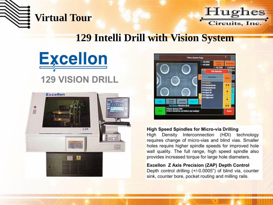
PRODUCTION Orbotech 9008 LDI Photo Plotter Multiline Tooling Direct Metallization Line Plasma Etch OEM Vacuum lamination Press Uniline 2000 Drill Concept 1 and 4 Drill Excellon 129 Vision Drill Excellon 300 Routers Excellon Co2 & UV laser Colight Photo Printers HAAS 3 Axis CNC Milling Center
Quality Control
Standard Quality Control Procedures
• 100% Netlist tested with a moving probe tester
• Cross sectioned to ensure acceptable verification and plating
• Coupons and cross sections available upon request
• All Inspectors are IPC 600 certified
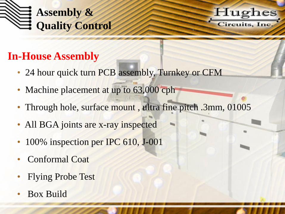
Assembly & Quality Control
• 24 hour quick turn PCB assembly, Turnkey or CFM
• Machine placement at up to 63,000 cph
• Through hole, surface mount , ultra fine pitch .3mm, 01005
• All BGA joints are x-ray inspected
• 100% inspection per IPC 610, J-001
• Conformal Coat
• Flying Probe Test
• Box Build
In-House Assembly
Conclusion
Printed circuit board quality is directly related to Manufacturing Expertise in a Controlled Environment Hughes Circuits has:
• Attracted high technology board designs too complex for the average . • Leveraged the knowledge gained from building complex board designs for the client’s benefit. • Developed processes and systems which reliably produce great boards whether simple or complex.
Conclusion
All this translates into a Great Partner for You You Made the Right Choice with Hughes Circuits
• Big enough to do the job perfectly • Small enough to have a personal touch • Always keeping clients informed and updated
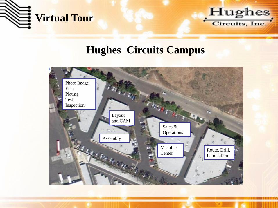
Virtual Tour
Hughes Circuits Campus
Route, Drill, Lamination
Photo Image Etch Plating Test Inspection
Layout and CAM
Assembly
Sales & Operations
Machine Center

Virtual Tour
Hughes Circuits Layout /CAM

Virtual Tour
Layout Process This image cannot currently be displayed.

Virtual Tour
IPC CID + Certified Layout
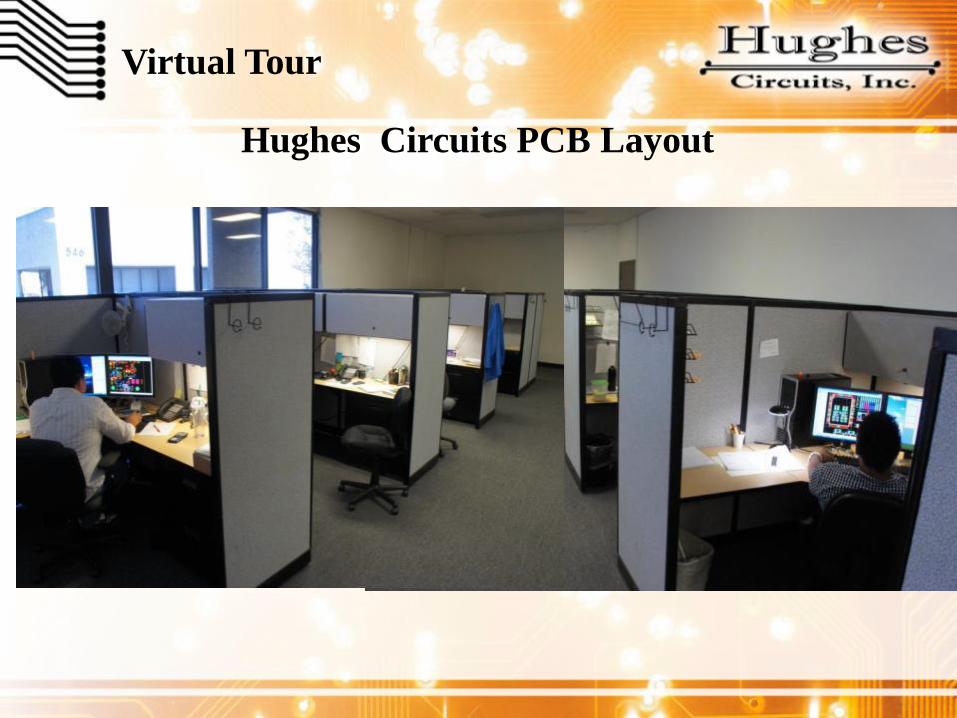
Virtual Tour
Hughes Circuits PCB Layout
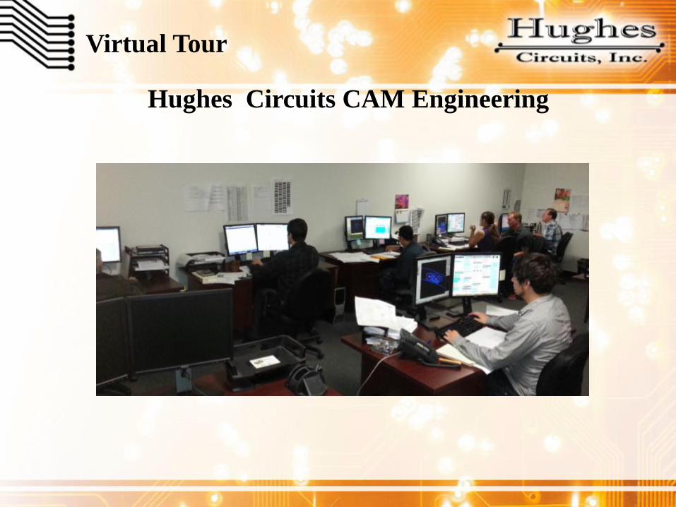
Virtual Tour
Hughes Circuits CAM Engineering

Virtual Tour
PCB Fabrication
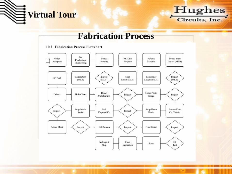
Virtual Tour
Fabrication Process This image cannot currently be displayed.

Virtual Tour
Photo Resist

Virtual Tour
Laser Direct Imaging
Virtual Tour
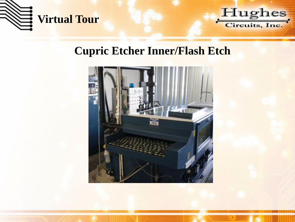
Cupric Etcher Inner/Flash Etch

Virtual Tour
Automated Optical Inspection

Virtual Tour
Lamination Presses
Virtual Tour
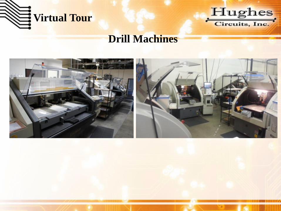
Drill Machines
Virtual Tour
129 Intelli Drill with Vision System

Virtual Tour
Lasers – Excellon Cobra and ESI CO2/UV

Virtual Tour
Plasma Clean/Etch
Virtual Tour
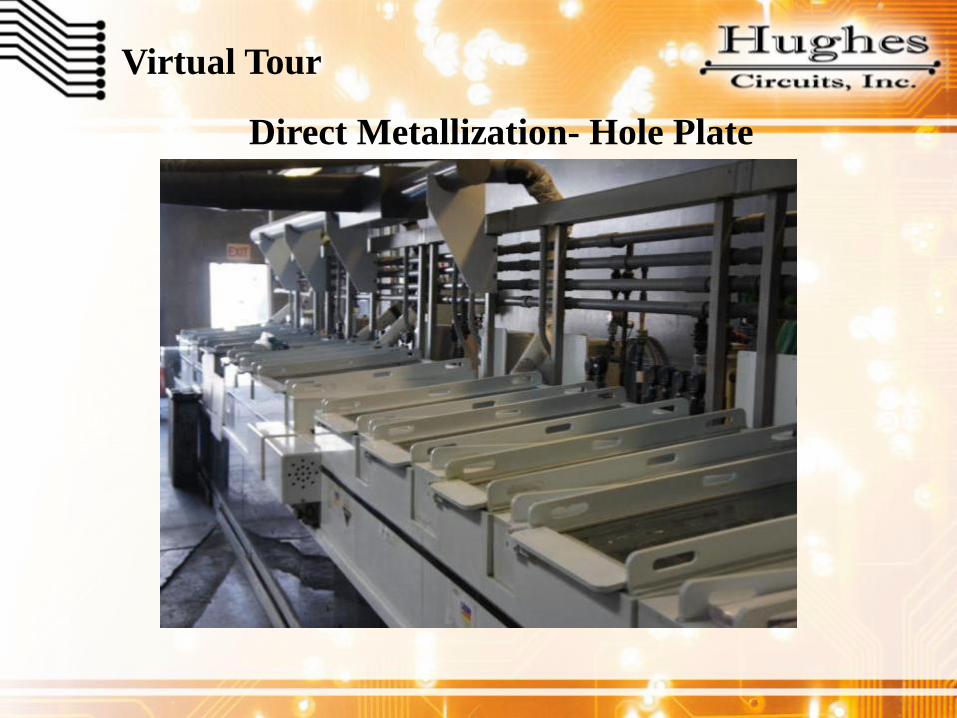
Direct Metallization- Hole Plate
Virtual Tour
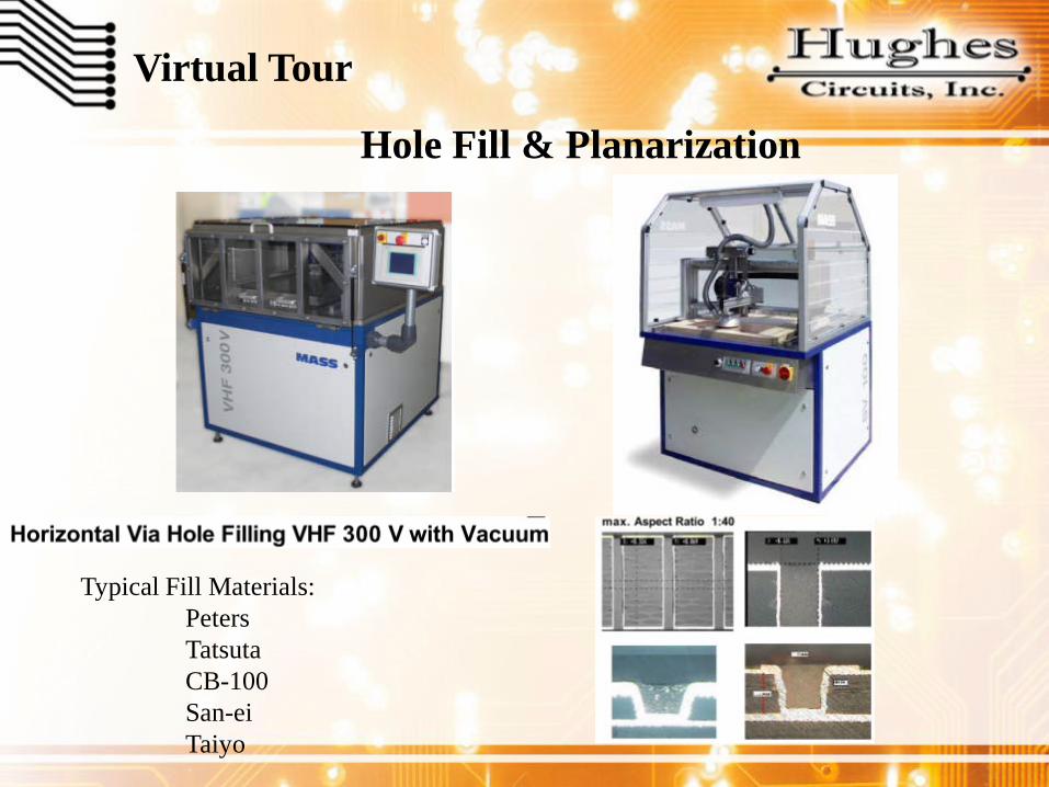
Hole Fill & Planarization
Typical Fill Materials: Peters Tatsuta CB-100 San-ei Taiyo
Virtual Tour
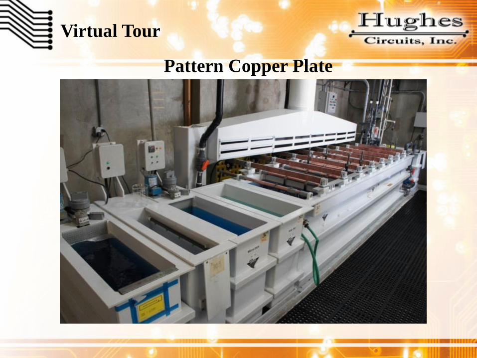
Pattern Copper Plate

Virtual Tour
Solder Plate
Virtual Tour
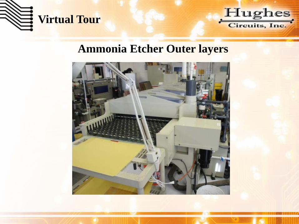
Ammonia Etcher Outer layers

Virtual Tour
Strip Solder
Virtual Tour
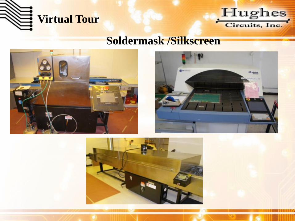
Soldermask /Silkscreen
Virtual Tour
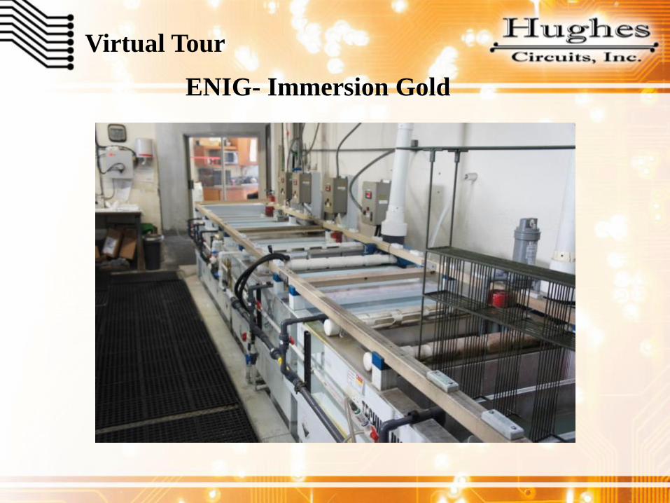
ENIG- Immersion Gold
Virtual Tour
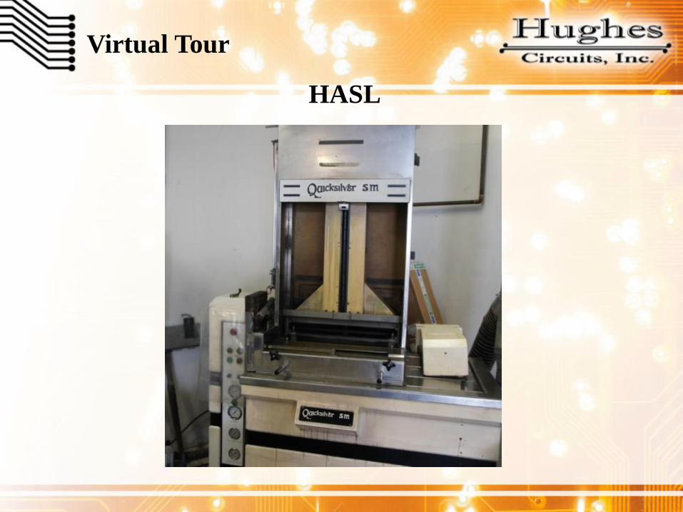
HASL

Virtual Tour
Soft / Hard Au , Imm Ag/Sn, ENIG, ENEPIG

Virtual Tour
Electrical Test
Virtual Tour
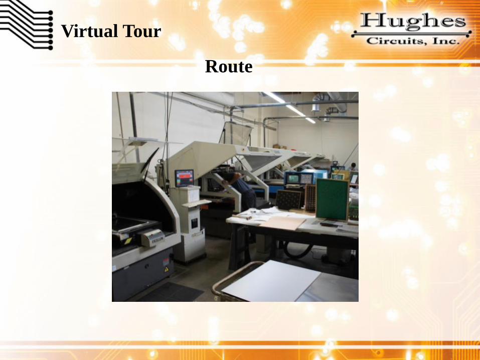
Route

Virtual Tour
Haas CNC Machine Center

Virtual Tour
V-Score

Virtual Tour
Optical Measuring System
Virtual Tour
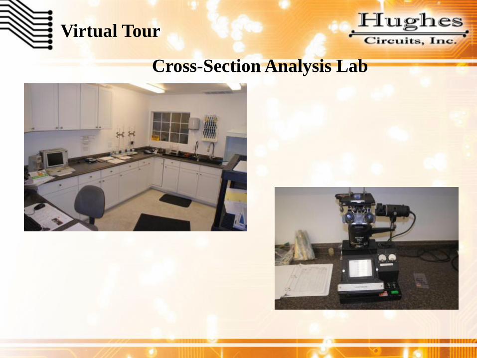
Cross-Section Analysis Lab

Virtual Tour
Impedance TDR & XRF
Zmetrix Impedance Test System CMI900 XRF

Virtual Tour
Assembly Operation
Virtual Tour
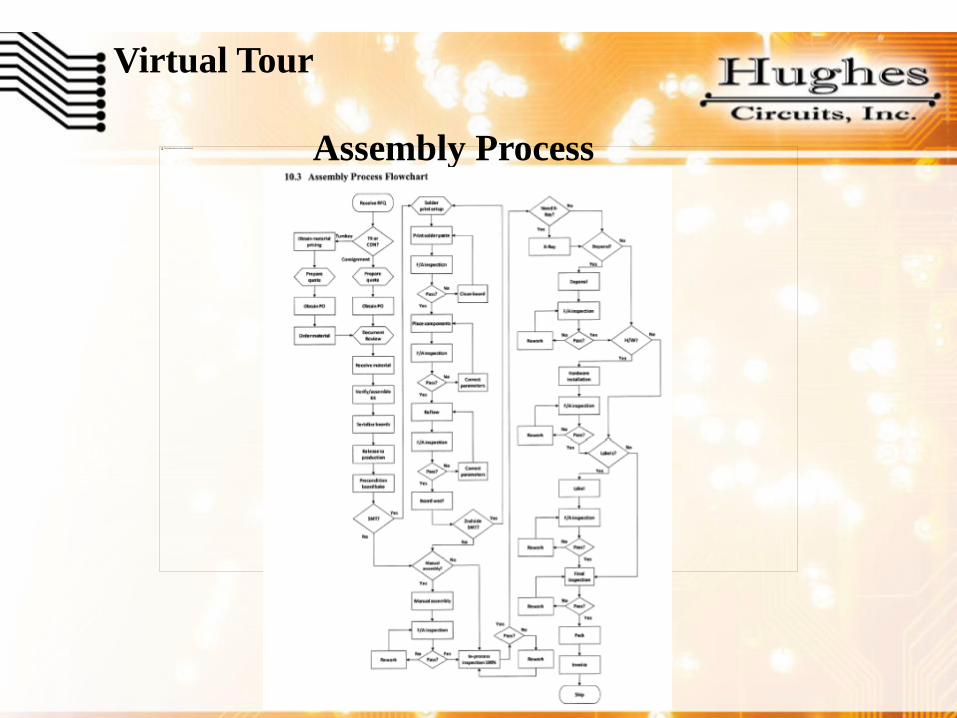
Assembly Process This image cannot currently be displayed.

Virtual Tour
SMT Area
Virtual Tour
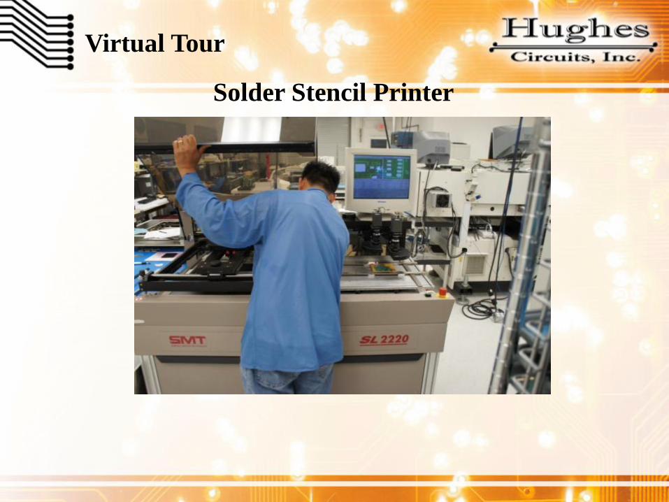
Solder Stencil Printer
Virtual Tour
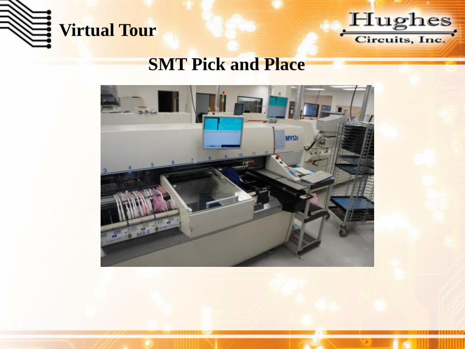
SMT Pick and Place

Virtual Tour
Reflow Ovens
Virtual Tour
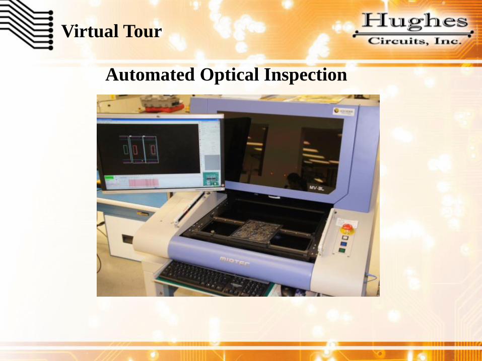
Automated Optical Inspection

Virtual Tour
Component X-RAY
Virtual Tour
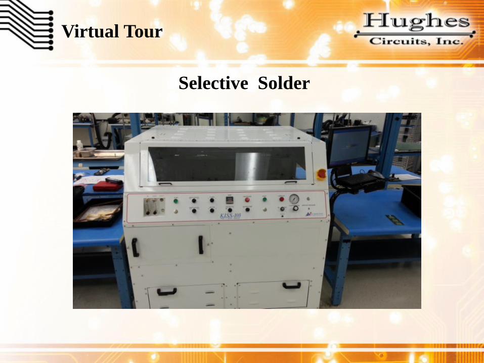
Selective Solder
Virtual Tour
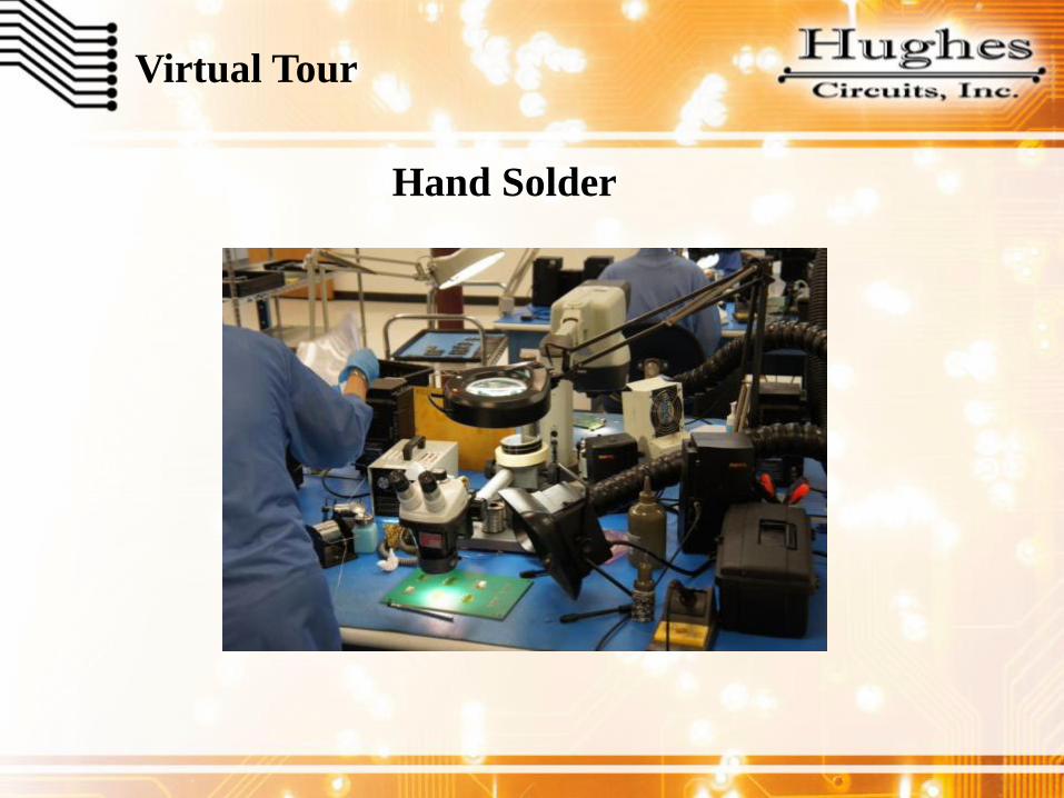
Hand Solder
Virtual Tour
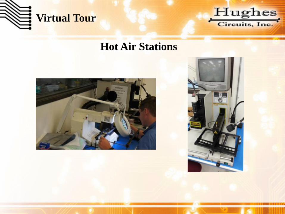
Hot Air Stations
Virtual Tour
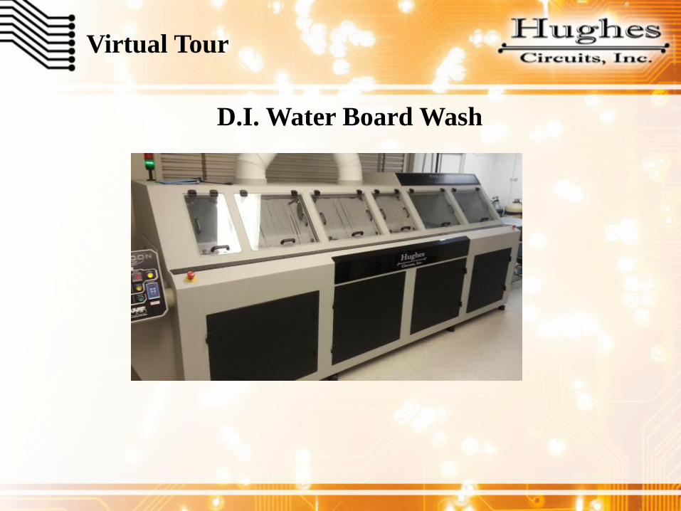
D.I. Water Board Wash
Virtual Tour
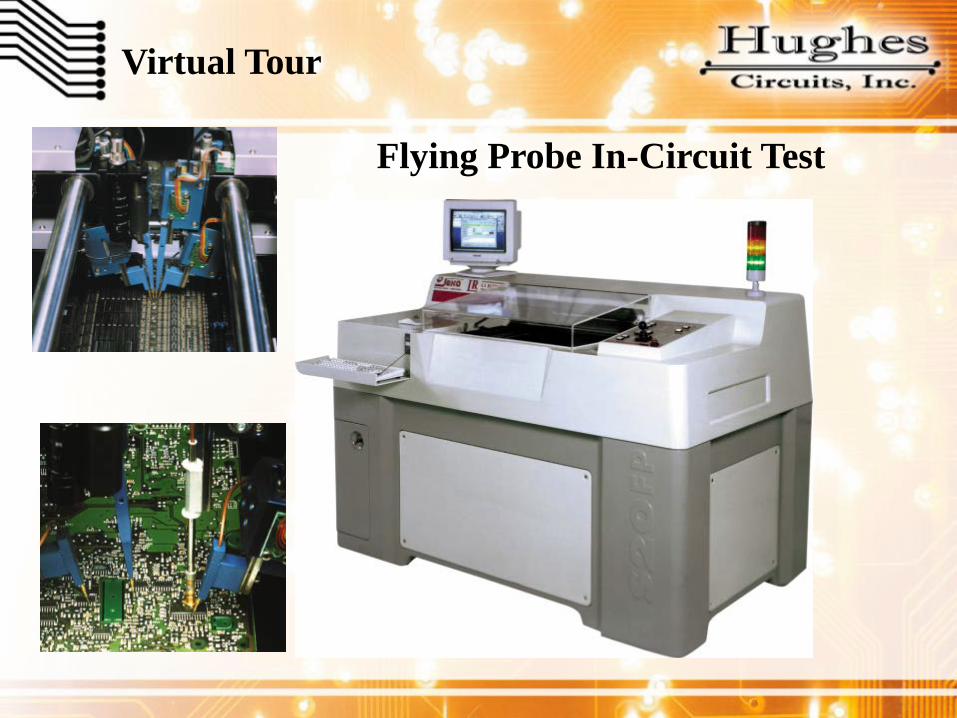
Flying Probe In-Circuit Test
Virtual Tour
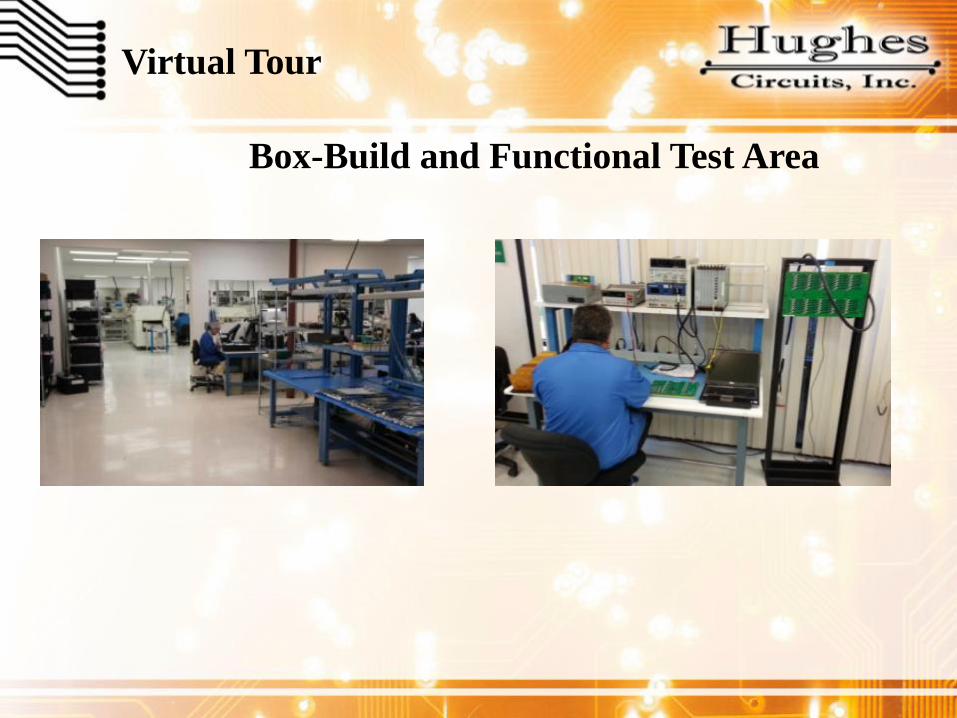
Box-Build and Functional Test Area

Virtual Tour
Final Inspection
Virtual Tour
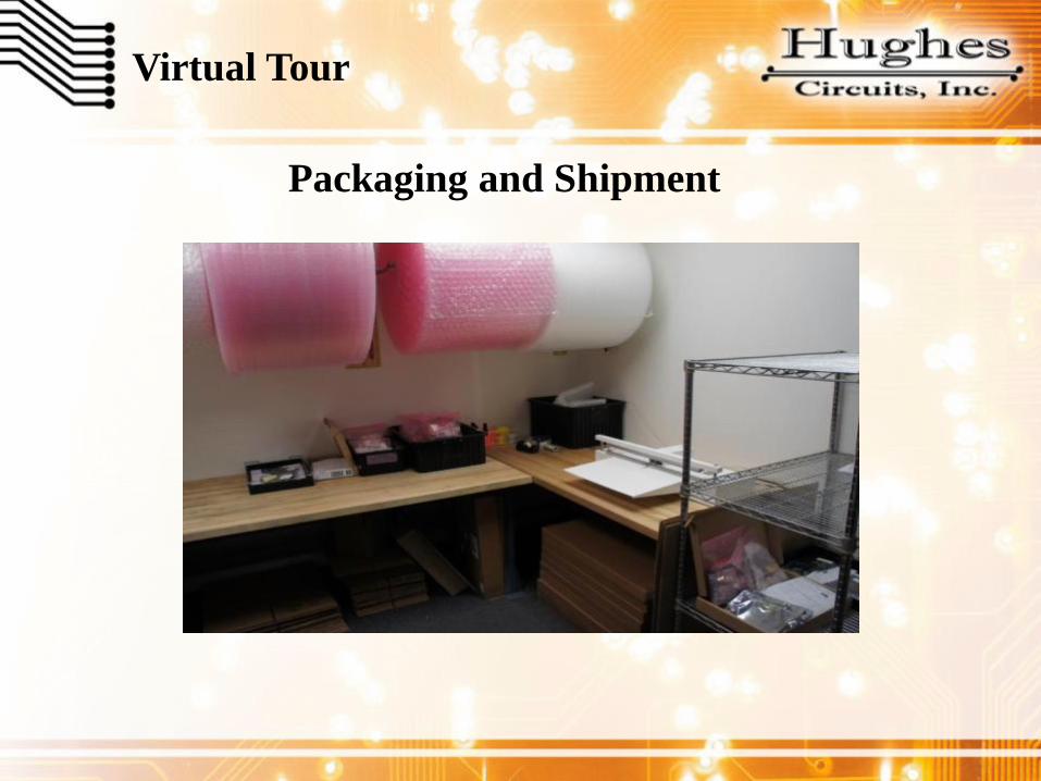
Packaging and Shipment

Virtual Tour
Thank you for visiting Hughes Circuits