74hc83.pdf
TRANSCRIPT

HD74HC83
4-Bit Binary Full Adder (with Fast Carry)
Description
This improved full adder performs the addition of two 4-bit binary numbers. The sum ( ) output areprovided for each bit and the resultant carry (C4) is obtained from the fourth bit.
This adder features full internal look ahead across all four bit generating the carry term in ten nanosecondstypically.
This provides the system designer with partial look-ahead performance at the economy and reducedpackage count of a ripple-carry implementation.
Features
• High Speed Operation: tpd (Ai or Bi to Zi) = 16 ns typ (CL = 50 pF)
• High Output Current: Fanout of 10 LSTTL Loads
• Wide Operating Voltage: VCC = 2 to 6 V
• Low Input Current: 1 µA max
• Low Quiescent Supply Current: ICC (static) = 4 µA max (Ta = 25°C)

HD74HC83
2
Function Table
Outputs
Inputs When C0 = L/When C2 = L When C0 = H/When C2 = H
A1/A3 B1/B3 A2/A4 B2/B4 ∑1/∑3 ∑2/∑4 C2/C4 ∑1/∑3 ∑2/∑4 C2/C4
L L L L L L L H L L
H L L L H L L L H L
L H L L H L L L H L
H H L L L H L H H L
L L H L L H L H H L
H L H L H H L L L H
L H H L H H L L L H
H H H L L L H H L H
L L L H L H L H H L
H L L H H H L L L H
L H L H H H L L L H
H H L H L L H H L H
L L H H L L H H L H
H L H H H L H L H H
L H H H H L H L H H
H H H H L H H H H H
H : High levelL : Low levelX : IrrelevantNote: Input conditions at A1, B1, A2, B2 and C0 are used to determine outputs ∑1 and ∑2 and the value of the
internal carry C2.The value at C2, A3, B3, A4 and B4 are than used to determine outputs ∑3, ∑4 and C4

HD74HC83
3
Pin Arrangement
1
2
3
4
5
6
7
8
A4
Σ3
A3
B3
VCC
Σ2
B2
A2
B4
Σ4
C4
C0
GND
B1
A1
Σ1
16
15
14
13
12
11
10
9
(Top view)
A4Σ3
Σ2
A3
Σ4
C4
C0
B1
A1
B3
B2
B4
A2 Σ1

HD74HC83
4
Block Diagram (1//2)
B4
B3
A4
A3
B2
A2
B1
A1
C0 Σ1
Σ2
Σ3
Σ4
C4

HD74HC83
5
DC Characteristics
Ta = 25°CTa = –40 to+85°C
Item Symbol VCC (V) Min Typ Max Min Max Unit Test Conditions
Input voltage VIH 2.0 1.5 — — 1.5 — V
4.5 3.15 — — 3.15 —
6.0 4.2 — — 4.2 —
VIL 2.0 — — 0.5 — 0.5 V
4.5 — — 1.35 — 1.35
6.0 — — 1.8 — 1.8
Output voltage VOH 2.0 1.9 2.0 — 1.9 — V Vin = VIH or VIL IOH = –20 µA
4.5 4.4 4.5 — 4.4 —
6.0 5.9 6.0 — 5.9 —
4.5 4.18 — — 4.13 — IOH = –4 mA
6.0 5.68 — — 5.63 — IOH = –5.2 mA
VOL 2.0 — 0.0 0.1 — 0.1 V Vin = VIH or VIL IOL = 20 µA
4.5 — 0.0 0.1 — 0.1
6.0 — 0.0 0.1 — 0.1
4.5 — — 0.26 — 0.33 IOL = 4 mA
6.0 — — 0.26 — 0.33 IOL = 5.2 mA
Input current Iin 6.0 — — ±0.1 — ±1.0 µA Vin = VCC or GND
Quiescent supplycurrent
ICC 6.0 — — 4.0 — 40 µA Vin = VCC or GND, Iout = 0 µA

HD74HC83
6
AC Characteristics (CL = 50 pF, Input tr = tf = 6 ns)
Ta = 25°CTa = –40 to+85°C
Item Symbol VCC (V) Min Typ Max Min Max Unit Test Conditions
Propagation delay tPLH 2.0 — — 150 — 190 ns C0 to ∑i
time tPHL 4.5 — 19 30 — 38
6.0 — — 26 — 33
tPLH 2.0 — — 150 — 190 ns Ai or Bi to ∑i
tPHL 4.5 — 16 30 — 38
6.0 — — 26 — 33
tPLH 2.0 — — 150 — 190 ns C0 to C4
tPHL 4.5 — 17 30 — 38
6.0 — — 26 — 33
tPLH 2.0 — — 150 — 190 ns Ai or Bi to C4
tPHL 4.5 — 18 30 — 38
6.0 — — 26 — 33
Output rise/fall tTLH 2.0 — — 75 — 95 ns
time tTHL 4.5 — 5 15 — 19
6.0 — — 13 — 16
Input capacitance Cin — — 5 10 — 10 pF

Hitachi CodeJEDECEIAJWeight (reference value)
DP-16ConformsConforms1.07 g
Unit: mm
6.30
19.20
16 9
811.3
20.00 Max
7.4
0 M
ax
7.62
0.25+ 0.13– 0.052.54 ± 0.25 0.48 ± 0.10 0.
51 M
in
2.54
Min
5.06
Max
0° – 15°
1.11 Max
Hitachi CodeJEDECEIAJWeight (reference value)
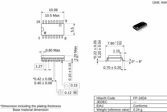
FP-16DA—Conforms0.24 g
Unit: mm
*Dimension including the plating thicknessBase material dimension
*0.2
2 ±
0.05
*0.42 ± 0.08
0.12
0.15
M
2.20
Max
5.5
10.06
0.80 Max
16 9
1 8
10.5 Max
+ 0.20– 0.307.80
0.70 ± 0.20
0° – 8°
0.10
± 0
.10
1.15
1.27
0.40 ± 0.06
0.20
± 0
.04

Hitachi CodeJEDECEIAJWeight (reference value)
FP-16DNConformsConforms0.15 g
Unit: mm
*Dimension including the plating thicknessBase material dimension
1.27
16 9
1 8
0.15
0.25 M
1.75
Max
3.95
*0.2
2 ±
0.03
9.9
0° – 8°
10.3 Max
+ 0.10– 0.306.10
+ 0.67– 0.200.60
+ 0
.11
– 0.
040.
14
*0.42 ± 0.08
0.635 Max
0.40 ± 0.06
0.20
± 0
.03
1.08