6l - tokushima u research of heuristic algorithm for optimization problems in lsi layout design for...
TRANSCRIPT

Vacuum
Si
SiO2
(eV)
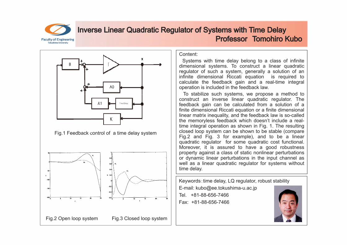
Content:Systems with time delay belong to a class of infinite
dimensional systems To construct a linear quadraticdimensional systems. To construct a linear quadraticregulator of such a system, generally a solution of aninfinite dimensional Riccati equation is required tocalculate the feedback gain and a real-time integraloperation is included in the feedback law.
To stabilize such systems we propose a method toTo stabilize such systems, we propose a method toconstruct an inverse linear quadratic regulator. Thefeedback gain can be calculated from a solution of afinite dimensional Riccati equation or a finite dimensionallinear matrix inequality, and the feedback law is so-calledthe memoryless feedback which doesn’t include a real-
Fig.1 Feedback control of a time delay system
ytime integral operation as shown in Fig. 1. The resultingclosed loop system can be shown to be stable (compareFig.2 and Fig. 3 for example), and to be a linearquadratic regulator for some quadratic cost functional.Moreover, it is assured to have a good robustnessproperty against a class of static nonlinear perturbationsor dynamic linear perturbations in the input channel aswell as a linear quadratic regulator for systems withouttime delay.
Keywords time delay, LQ regulator, robust stabilityE-mail: [email protected]. +81-88-656-7466Fax: +81-88-656-7466
Fig.2 Open loop system Fig.3 Closed loop system

A study on histological Matts grade estimation by computer-aided blood vessel image processing for the large intestine endoscopic images
Prof Shinsuke Konaka
Content:The ulcerative colitis is appointed in an intractable disease in
Japan to repeat a recurrence by the inflammatory disease that a sore
Prof. Shinsuke Konaka
Japan to repeat a recurrence by the inflammatory disease that a soreand the ulcer are formed on the mucous membrane (the inside) of the large intestine. The endoscope is used for the diagnosis. The purpose of this study is to support diagnosing it by computer image processing for the blood vessel pictures of the large intestine inside. By the blood vessel image extraction and characteristic parameter Fig. 1 A large intestine endoscope image and a blood vessel
extraction result research, the degree of inflammation from the state of a mucous membrane would be intended to estimate by the image processing instead of the histological classification.
At first, blood vessels are extracted from an endoscope image, as shown in Fig. 1, and the blood vessel characteristic parameter is researched that is effective to estimate an inflammatory diagnosis
extraction result
Grade 2 Grade 3
researched, that is effective to estimate an inflammatory diagnosisdegrees. The matching filter of the Gaussian distribution type is used to extract blood vessels. By changing the threshold value for the binarization, blood vessel number is computed through labeling process for each threshold value. The curve profiles of the blood vessel number are shown in Fig.2 for the histological Matts grades of Fig. 2 Extracted blood vessel numbers curves for each histological
Grade 5Grade 4
g g g2 of slight illness to 5 of most serious case. Figure 2 includes 23 cases so that 23 curves are shown in total. Shapes of curve profile for each the histological grade level are clearly different, that is, the lower grade shows the flatter curve profile. To examine our image processing performance, the correlation between the Matts grade of 2
g gclassification of Matts grade from 2 to 5
Max of B
loo
to 5 and maximum of blood vessel numbers are shown in Fig. 3. As the results, the correlation coefficient is as good as R = 0.833.
Keywords Large intestine endoscope image, blood vesselextraction, Matts grade evaluation by computer-aided image
od Vessel N
o.
processing
E-mail: [email protected]. +81-88-656-7469
Fig. 3 The good correlation between the histological Matts grades and extracted maximum of blood vessel numbers
Matts Grade

InGaAlN and AlC LEDs are researched.
A high voltage LED is developed. (Fig.1)
Ta-GaN is etched to sapphire during growth, and GaN, theepitaxial layer, is peeled off on Si, for example. (Fig.2)
Nano-pattern is formed on GaN, and their far field pattern areviewed as shown in Fig.3 (a) r=200 nm, (b) r=300 nm, (c)r=400 nm and (d) r=500 nm. It is clear that the 6th fold patternis clearly visible for 200 nm which is 6 times for the emittinglight.
P-type Mg-Ga1-xAlxN for x>0.3 is affected by the too deeplevel of Mg from the valence band, and it becomes aninsulator, while C-doped AlGaN is possible candidate for p-type conduction. We are making an effort to make carbon-doped AlGaN or AlN a p-type conduction.
We are growing AlC on sapphire, SiC and Si. SEM and X-rayrocking curve are shown in Fig.4, where a substrate issapphire.
Keywords:MOCVD, LED, AlGaInN, AlCE-mail: [email protected].: +81-88-656-7446Fax: +81-88-656-7446
crack
顔写真(省略可)
Fig.1 Fig.2
Fig.3
Fig.4

Content:Research of heuristic algorithmfor optimization problems in LSI layout design
For example,Obstacle avoiding rectilinear steiner tree (Fig.1)Voltage assignment in floorplan (Fig.2)3-D IC floorplanning with TSV co-placement
Fig.1 Obstacle avoidingrectilinear steiner tree
Keywords Heuristic Algorithm, Optimization Problem,LSI Design
E-mail: [email protected]. +81-88-656-7483Fax: +81-88-656-7471
Fig.2 Voltage assignment in floorplan

Content:There must be some electrical and magnetical influences in
biological body and bioelectrics is a field of pulsed powerV]
150
100 biological body and bioelectrics is a field of pulsed powerapplications recently. Pulsed power is technology of applyinghigh compressive power pulse and according to the electricmagnetism and we have focused on green technology andbioelectrics in applications of pulsed power. Some appliedresearches for effects of electrical pulses on biological body
100W X 1s
10GWX
10ns
Pow
er
Time
Vo
lta
ge
[k
100
50
0
-10 0 10 20
Fig.1 What is pulsed power Fig.2 Ns voltage pulse
researches for effects of electrical pulses on biological bodyare introduced here.
Different parameters of electric pulses as spectrum wouldbring different actions and responses on biological body orcells. The control of the parameters and responses willintroduce new biological applied-technologies The responses
TimeTime [ns]
10 0 10 20
pulsed powerintroduce new biological applied technologies. The responsesand their mechanisms, however, have not been still clear. Theeffects of electric pulses on various object and theirmechanisms have been studied and gene expression level asa response has been particularly considered. Some examplesof applied study using electric pulses are as follows: new
needle electrodes
pulsed power generator
controlnsPEFs
120
100
80
60
40
20
tum
or w
eigh
t [m
g]
(a) New cancer therapy
of applied study using electric pulses are as follows: newcancer therapy, production of biomass fuel from micro algae,and effects on endoplasmic reticulum stress responses forpulsed electric fields for prevention or therapy of disorders.
fertilized egg (tumor)20
0
(b) Production of biomass fuel (c) Control of
Keywords pulsed power, bioelectrics, pulse electric fieldE-mail: [email protected].: +81-88-656-7463Fax: +81-88-656-7463(b) oduc o o b o ass ue (c) Co o o
gene expressionFig.3 Studies of application of electric pulses
HP : jemez.ee.tokushima-u.ac.jp/lab/

Content:The performance of communication network has
been drastically enhanced by adopting fiber-opticWD
Transmission FiberWD been drastically enhanced by adopting fiber optic
transmission technologies into the backbone networksand access networks. Recently, the demand forcommunication capacity is increasing even more,because of popularization of cloud type-application andtransportation of ultra-broadband contents such as high-
Optical Amplifiers(Repeaters)
M
Optical Transmitters
Optical Receivers
Optical transmission distance
DM
p gdefinition moving pictures. The purpose of our laboratoryis bringing a significant progress of communicationnetwork by introduce novel functionality into the opticalcommunication network.
One of our topics of research is expanding optical
Fig.1 Configuration of backbone optical fiber transmission system
/2
p p g ptransmission distance in backbone networks (Fig.1) byintroducing phase-sensitive optical amplifiers (PSA)(Fig.2) as optical amplifier repeaters. The PSA amplify in-phase and de-amplify quadrature component withreference to phase-locked pump light in parametricamplifiers. From the fundamental operation, significantextension of optical transmission distance is expected.
Pump Laser Optical PLL*
(a) Fundamental operation of PSA
(*PLL Ph Keywords optical communication,optical fiber, optical amplifieroptical signal processing
E-mail: [email protected] Parametric Medium
p Optical PLL
Photo DiodeOptical HybridInput
Output
(*PLL : Phaselock loop)
Tel. +81-88-656-7465Fax: +81-88-656-7465
Fig. 2 Optical parametric phase sensitive amplifier (PSA)
(b) Basic configuration of PSA

Content:Highly polarized UV emission devices were expected
to develop the applications such as high resolutionnbar
1 to develop the applications, such as high resolutionimaging, high sensitive sensors, etc. The compactpolarization control device with high transmittance isrequired in order to develop integrated device for theseapplications.
One of the candidates to overcome the issue is the
Period Wavelength
1
(b) Periodic distribution of refractive index for light
(a) Schematic diagram One of the candidates to overcome the issue is thedevice using high contrast dielectric subwavelengthgrating (SWG) structure. In SWG, the pitch of the gratingis shorter than the wavelength of incident light. The Blochlike eigen-modes within SWG region resulting from thespatial periodicity of refractive index distribution interacts
Fig.1 Sub-wavelength grating structure(a) Schematic diagram
p p ywith incident light. As a result, the desirable opticalcharacteristics such as broadband high reflectivity andpolarization sensitivity are obtained with optimalstructures.
We have investigated the polarization characteristics ofg pAlGaN-based UV-LED with SWG fabricated on the top ofLED surface, and demonstrated the feasibility of highpolarized UV-LED grown on c-plane sapphire.
Fig.2 Electrical field distributionfor TM light by FDTD theory(in case of / =1.8)
Fig.3 Fabricated sub-wavelengthgrating on UV-LED surface
Keywords photonic device, sub-wavelength grating,polarization control, nano device
E-mail: [email protected]. +81-88-656-7447Fax: +81-88-656-7447
Fig.4 Emission spectra from UV-LED
Fig.5 Polarization ratio from UV-LED with sub-wavelength grating

Graphene is very promising for future micro- and nano-electronic systems, because of its outstanding properties.Now, our main research interest is “graphene on SiC”.We can fabricate 10 mm-sq single-crystal mono-layergraphene using super-RTA (rapid thermal annealer). Thehigh-quality and uniform epitaxial graphene was grownon controlled step structures of 4H-SiC (0001) substrate.Graphene properties were evaluated using various kindsof nano-metrology tools. By using scanning probemicroscopy (SPM), contact conductance betweennanoprobe and graphene was measured. The contactresistance value was estimated to be the order of 10-9
cm2. The novel phenomena of graphene nanomembranewith bistable contact conductance states was observed.This electro-mechanical bistability of atomic layer switchcould represent a new path to nano-electro-mechanicalsystems. A final goal of our graphene research will benew functional devices for the post-Si era.
Keywords: graphene, SiC, nano-metrologyE-mail: [email protected]. +81-88-656-9716Fax: +81-88-656-9716HP : http://graphene.ee.tokushima-u.ac.jp/

Content:1. Chaos Cryptosystems
Sensitive dependence of chaos on initial conditionsSensitive dependence of chaos on initial conditionsand parameters is exploited for various securityissues.
2. Chaos Communication SystemsContinuity of chaotic sequences generated from anid ti l h ti i l it d t d t
Fig. 1: Logistic map, Fig. 2: One-parameterone of the most famous bifurcation diagram of theone-dimensional map Logistic map.
identical chaotic map is exploited to recover datacorrectly.
3. Complex NetworksVarious synchronization phenomena in coupledchaotic circuits are good models of various complexone dimensional map Logistic map.
generating chaos.g p
networks.4. Nonlinear Time Series Analysis
Chaos analysis is utilized to predict a trend ofnonlinear time series or to diagnose medical signals.
5 Data Mining5. Data MiningSelf-organizing feature of artificial neural networks isexploited to carry out clustering of various data.
Fig. 3: Four autonomous Fig. 4: Four-phasechaotic circuits coupled quasi-synchronization
Keywords chaos, chaos cryptosystems,chaos communication systems, complexsystems, nonlinear time series analysis
E-mail: [email protected]>Tel +81 88 656 7470p q y
by one resistor. of chaos observed fromthe circuits in Fig. 3.
Tel. +81-88-656-7470Fax: +81-88-656-7471HP : http://nlab.ee.tokushima-u.ac.jp/nishio.htm

Content:BGA ICs have been often used for realizing electric
circuits of smaller size The ICs are soldered on a finecircuits of smaller size. The ICs are soldered on a finepitched PCB. Open defects may occur at interconnectsbetween the ICs and the PCB in the soldering process.An example of the defects is shown in Fig.1. Theinterconnects are impossible to be observed by visualinspection. Also, logic signals of the interconnects canp , g gnot be measured with a test probe. Thus, IEEE 1149.1test circuit has been implemented inside the ICs.
However, open defects may not be detected, even ifthe circuit is implemented inside an IC. Also, it is difficultto generate test input vectors for detecting open defects
(a)Assembled printed circuit boards
g p g pand locating defective interconnects. Thus, we aredeveloping electrical test methods and DfT(Design-for-Testability) methods for open defects in the interconnects.
One of our test methods is shown in Fig.2. Ourmethods are based on supply current that is made flow in
(b)Open defect occurring in soldering processFig.1 Targeted defects pp y
our tests. Soft open defects that generate only additionaldelay time can be detected and the defectiveinterconnects can be located together with hard opendefects that generate logical errors with our test methods.
Keywords electrical test, printed circuit board,soldering error , open defect
E-mail: [email protected]. +81-88-656-7473Fax: +81-88-656-7473HP : http://tameone.ee.tokushima-u.ac.jp/tume/Fig.2 Electrical test of assembled PCB

Content:1. Phasor measurements at demand sides and its
applicationsDeveloping an online monitoring of power system by multiple phasor measurement units with monitoring voltages at the outlets on the wall.
2. Management of distribution network with high penetration of photovoltaic generation unitsInvestigating reasonable voltage regulation on high and low voltage distribution lines by cooperation of photovoltaic generation units and other apparatus.
3. Advanced power conversion to integrate multiple dc energy sourcesIntegrating multiple dc voltage terminals to connect solar cells, batteries and loads easily, based on multi-level converter topology with flying capacitors.
4. Power modulations of distributed energy resources for frequency controlDeveloping a voltage phasor modulation of grid-connected converters to regulate the system frequency as much as possible.
Keywords: smart grid, reliability, stability, quality, electricvehicles, renewable energy resourcesE-mail: hojo @ ee.tokushima-u.ac.jpTel. +81-88-656-7452Fax: +81-88-656-7452
crack
Fig. 1. My major researches.
Fig. 2. Online monitoring. Fig. 3. Dc sources integration.

Content:In recent years, various systems coexisted within
human such as industrial machines and life supportsystems tend to increase. In addition, a highperformance and a high accuracy for these systems arestrongly required. To meet these requirements, we makeapplied researches on a control system using anintelligent information processing technique on the basisof biologically inspired approaches. For example, wepropose the design and implementation methods of thecontrol system combining soft-computing techniques(fuzzy, neural network, etc.) and control theories. Currentresearch themes are listed below:
Output prediction of wind or photovoltaic powergenerator using weather forecast modelCooperative control of multiple mobile robot systemAdaptive gait control for quadruped robot using centralpattern generator networkOperator’s support system for remote controlled robotMotion control of power assist knee orthosisSafety driving support system of electric wheel chair
Keywords intelligent control, robot, wind energy andphotovoltaic power generation,rehabilitation system
E-mail: [email protected]. +81-88-656-7458Fax: +81-88-656-7458HP : http://www-sky.ee.tokushima-u.ac.jp
Quadruped robot
Renewable energy system Remote control mobile robot
Electric wheel chair Multiple mobile robots
Developed experimental system in our lab.
Power assist knee orthosis

Content:With the miniaturization of silicon transistors in the end of
20th century, there was rapid development in the computery, p p pinformation systems. The guiding principle is the scaling rule.With the decreasing of the device dimensions, high speed,low power consumption, high density integration, low price arespontaneously realized. To expand the potentials of themicroelectronics to the application on communication,consumer electrical appliances lighting and power electronicsconsumer electrical appliances, lighting and power electronics,it is necessary to achieve high voltage and high power. Tomaintain the high voltage and miniaturization compatibly,silicon technology is limited. It is necessary to introduce widebandgap semiconductors. A prospective candidate is galliumnitride (GaN). GaN blue light emitting diodes have alreadyb i li d It i l b i d l d t libecome commercialized. It is also being developed to realizegeneral lighting as a white source. In this laboratory, using thesame material of GaN, transistors, diodes, chemical sensorsand integrated circuits are being developed for theapplications in microwave communication and powerelectronics. Recently, in detail, we are focusing on GaNy gSchottky diode for microwave rectification, high-frequencyAlGaN/GaN HFET using electron-beam lithography, E-modeGaN MOSFET for power electronics and chemical sensor onAlGaN/GaN heterostructure
Keywords wide bandgap semiconductor,electron device, sensormonolithic integrated circuit.E-mail: [email protected] +81 88 656 7442Tel. +81-88-656-7442Fax: +81-88-656-7442HP : http://wwww.ao-lab.net

Since the electrical characteristics of graphene field-effect transistors (FETs) are very sensitive for theirenvironmental condition, the graphene FETs have highpotential for chemical and biological sensors. In ourlaboratory, various sensors based on graphene FETs areinvestigated. The graphene FETs can be operated in thebuffer solution by top-gated operation from a referenceelectrode without any passivation film owing to their largepotential window. And their transconductance was morethan 200 times larger than that of the conventional back-gated operation in vacuum. The drain current increasedwith increasing the solution pH. And the graphene FETsdetected the charges in proteins. To detect the specificprotein, aptamers were functionalized on the graphenesurface. As a result, Aptamer-modified graphene FETsdetected the target molecule, and their sensitivity wascomparable for other aptamer-based biosensors.
Keywords graphene, device, biosensorE-mail: [email protected]. +81-88-656-7439Fax: +81-88-656-7439HP : http://graphene.ee.tokushima-u.ac.jp/
0 10 20 30 40 50 6034.8
35.2
35.6
36.0
36.4
IgESA
Drai
n cu
rrent
(µA)
Time (min)
BSA
-0.10 -0.05 0.00 0.05 0.10
0.15
0.18
0.21
0.24
7.85.84.8
Cond
ucta
nce
(mS)
Top-gate voltage (V vs Ag/AgCl)
pH 4.0
Graphene device fabrication
5 µm
Graphene FET Graphene-FET based biosensors
0 20 40 60 80 100
8
10
128.2
7.87.2
6.6
5.8
5.14.94.84.6Drai
n cu
rrent
(µA)
Time (min)
4.04.3pH
Detection of solution pH
Sensing results
Receptor functionalization and specific protein detection

Content:Sudden cardiac arrest is a major public health problem
and Ventricular Fibrillation (VF) and Ventricularand Ventricular Fibrillation (VF) and VentricularTachycardia (VT) are serious arrhythmic events in mostof patients suffering from sudden cardiac arrest. Forthese serious arrhythmic events, the timely employmentof an electrical defibrillator may lead to successful results.
Fig.1 Sinus Rhythm (Left) and its Scalogram (Right)VF is the most serious variety of arrhythmia whichrequires accurate and quick detection to save lives. Thuswidespread deployment of automated externaldefibrillators (AEDs) has been suggested and a pivotalcomponent in AEDs is the detection of VF and VT byp ymeans of appropriate algorithm. However, reliable,accurate and quick detection of ventricular arrhythmia isnot easy.
From this viewpoint, on the basis of Wavelet Transform(WT) h d d t ti l ith f
Fig.2 VF (Left) and its Scalogram (Right)
(WT) we have proposed some detection algorithms forelectrocardiogram (ECG). Fig.1--3 show ECG signalsand normalized scalogram. The proposed algorithmconsists two stage detection and achieves goodperformance comparing with the existing results.
Keywords detection algorithm, wavelet transform,defibrillation, VF, VT, PEA, SR,sudden cardiac arrest
E mail hide o@ee tok shima ac jp
Fig.3 VT (Left) and its Scalogram (Right)
E-mail: [email protected]. +81-88-656-7467Fax:+81-88-656-7467

Development of Diagnostic Techniques for Power EquipmentUsing Radio Remote Sensing and Signal Processingg g g g
Associate Professor Masatake KawadaContent:1. SubjectC f lt d t d t i ti ti t d
Development of Insulation Diagnostic Techniques for Distribution Line Using FDTD Method Partial Discharge
Transformer Can faults due to deterioration over time or unexpectedfaults occurring in power equipment be detectedbeforehand ?2. Research ContentsHow to detect a symptom of faults ?
Transformer
Antennas How to detect a symptom of faults ?
(1) Radio Sensing, to locate deterioration of insulatingmaterials(2) Signal Processing, to locate abnormal positions inturbines, generators, and pumps
0 20 40 60 80 100 120-1.5-1
-0.50
0.51
1.5
E z (V/m
) Direction of Arrival Estimation
, g , p p3. Record of Joint Research(1) Chubu Electric Power Co. Inc. and Mitsubishi HeavyIndustries Ltd. for diagnosing turbine generators(2) Chubu Electric Power Co. Inc. and Hitachi Ltd. for
0 20 40 60 80 100 120.5Time (ns)
Detection of Abnormal Vibration Using Wavelet Transform
Electromagnetic Waves Emitted from Partial Discharge, which is a Symptom of Degradation of Insulating Materials.
( )diagnosing pumps(3) Railway Technical Research Institute for diagnosingground coils of superconducting Maglev
Keywords Radio Sensing and Signal ProcessingE-mail: [email protected]>Tel. +81-88-656-7460Fax: +81-88-656-7460HP:http://pub2.db.tokushima-u.ac.jp/ERD/person/25080/profile-en.htmlTime-Frequency Visualization of Abnormal
Vibration

With the widely spread of video applications, novel codingalgorithms which can answer many kinds of emergingdemands are highly required. Our research group is devotingde a ds a e g y equ ed Ou esea c g oup s de ot gto propose good ideas concerning the following themes.1. Improvements of the algorithms of HEVC and its low
complexity and low power VLSI architecture for the nextgeneration applications which are over 4K resolutions. Thealgorithms and architectures are concerning the intraalgorithms and architectures are concerning the intracoding, motion estimation, and deblocking filter.
2. Scalable video coding algorithms which are suitable forhigh resolution applications. We will make full use of thehigh correlations between base layer and enhancementlayer to propose new algorithms to improve the codinglayer to propose new algorithms to improve the codingefficiency.
3. Highly parallel processing video coding algorithms onmany-core platforms. Most of traditional coding algorithmsutilize the coding parameters of adjacent blocks toimprove coding efficiency However this coding structureimprove coding efficiency. However, this coding structurehas essential demerit for parallel processing. As shown inFig.2, our motivation is to find new coding structure whichcan achieve higher parallel coding performance.
Keywords H.265/HEVC, Scalable Video coding(SVC),Parallel Video Coding

Content:Discharge plasma reactors consisting of a massive high
voltage generator and discharge electrodes are more likely tovoltage generator and discharge electrodes are more likely tobecome large-scale system. We have proposed and studiedvarious types of compact plasma reactors using piezoelectricdevices. Piezoelectric transformers (PTs) that act as compacthigh-voltage generator have been widely embedded in abacklight invertor for LCDs. Our proposed plasma reactors
(b) Discharge plasma
backlight invertor for LCDs. Our proposed plasma reactorsfeature compact configurations because the devices serve asboth high-voltage source and discharge electrode. Non-thermal plasmas, such as corona discharge, glow dischargeand dielectric barrier discharge (Fig. 1(a)(b)) can be producedusing the plasma reactors. Several applications of the plasmag p pp preactors to ozone generators (Fig. 1(c)) and vacuumultraviolet light source have been demonstrated.
We have also promoted actively other research ingeneration, diagnosis and applications of non-thermalatmospheric pressure plasma, including in-situ measurementFig 1 Compact plasma reactor using piezoelectric device and its
(a) Configuration (c) Application to ozone generatoratmospheric pressure plasma, including in situ measurementof ozone density inside DBD ozone generator (Fig. 2) andsurrounding gas-fed (SGF) plasma jet (Fig. 3).
Fig. 1 Compact plasma reactor using piezoelectric device and itsapplication
Ozonizer DPSS laser
Keywords Dielectric barrier discharge,ozone, plasma jet
E-mail: [email protected]. +81-88-656-7454Fax: +81 88 656 7454
(a) He/Air
(b) H /O
Photodetector
Fax: +81-88-656-7454http://pub2.db.tokushima-u.ac.jp/ERD/person/155803/profile-ja.html
(b) He/O2
Fig. 3 SGF Plasma jetFig. 2 In-situ O3 measurement by laser optical absorption

Content:We are studying the ablation and modification of materials
i t ith f t d l i di ti I dditiassociates with femtosecond laser irradiation. In addition, weare also interested in the transient state of materials duringfemtosecond laser irradiation.
The schematic of time-resolved soft x-ray imaging of ablationd th fl ti i l ti t h d lprocesses and the reflective images on platinum at each delay
time are show in Fig. 1. From this figure, it was found that theablation phenomena is already started at 10 ps, and finishedat 160 ps. We also observed the nano-bubble formation andnonthermal ablation processes related to the femtosecondlaser irradiation.
Fig. 2 shows the schematic of electrical conduction controlby fs laser modification. The femtosecond laser beam isirradiated between two metal contacts on semiconductor. Withincreasing the irradiation fluence, the local electricalconductivity abruptly decreased at the threshold fluence.Fig.1 : Schematic of time-resolved soft x-ray imaging of ablation
processes and the reflective images on platinum at each delay time
Keywords femtosecond laser, ablationE-mail: [email protected]. +81-88-656-7445Fax: +81-88-656-7445HP : http://pub2.db.tokushima-u.ac.jp/
ERD/person/ 82121/profile-en.htmlFig.2 : Electrical conduction control by fs laser modification

Content:Nitride semiconductors are one of the most attractive
candidates for LEDs The problem of the crystal growthcandidates for LEDs. The problem of the crystal growthof nitrides is no suitable substrate with good latticematching and low price.In order to obtain nitride substrates at low cost, we grow
GaN by a direct synthesis method (DSM) and AlN by a
Cross sectionSurface
c-faceGaN
(a)
y y ( ) ysublimation method (or physical vapor transport). Bothmethods are low-cost growth method.Figure 1(a) shows the surface and cross sectional
images of the c-face GaN grown on c-plane sapphire and(b) f G N l hi B th l(b) (b) a-face GaN on r-plane sapphire. Both grown layersare relatively high quality and can be used as substratesfor the growth of nitrides.Figure 1(c) shows the AlN layer grown by a sublimation
method. The grown layer is relatively high quality. We50 m50 m
a-faceGaN
(b)
g y y g q ygrew AlGaN by MOCVD on the AlN substrate and thegrown AlGaN layer shows good luminescence.
f AlN
(c)
Keywords AlN, GaN, bulk crystal growthE-mail: [email protected]>Tel. +81-88-656-7464Fax: +81-88-656-7464
c-faceAlN
Fig.1: Surface and cross sectional gimages of the grown layers.

Content:In recent highly integrated VLSIs, cost of testing is a
j bl T ll i t th diffi lt i t ti d imajor problem. To alleviate the difficulty in testing, designfor testability techniques are widely used. In our researchlab, we develop methods for reducing test cost such astest data volume, test application time, area overhead oftest circuit and for improving test quality especially intest circuit, and for improving test quality especially indelay testing. One of the techniques is design fortestability method for small delay faults using time-to-digital converter embedded in boundary scan calledTDCBS, shown in the figures. The boundary scan cells, g yare modified to be able to form a time-to-digital converterthat is utilized for detecting delay. Using this architecture,defects like opens and shorts can be detected as extradelay caused by such defects even if the delay is small
Fig.1 overview of design for testability
and cannot be detected by conventional logic test. Thefeasibility of the proposed methods is estimated by bothsimulation and experiments of fabricated chips.
Keywords design for testability, VLSI testing,delay faults, test cost reduction
E-mail: [email protected]. +81-88-656-9183Fax: +81-88-656-9183
Fig.3 layout of an experimental chip
Fig.2 Boundary scan with TDC

Content:According to the vital statistics from Ministry of Health,
Labour and Welfare 33% of Japanese are died byLabour and Welfare, 33% of Japanese are died bydiseases related to the circulatory system. It is well-known that diet modification and an appropriate exerciseare effective to prevent these diseases. If we have aportable device which can evaluate the circulatoryFig 1. Prototype of a measurement device for blood system and exercise habit, it is expected to suppressthese diseases and medical care costs.We have developed a portable measurement device
(Fig. 1) for blood flow velocity (BFV) and investigated therelationship to various conditions for hundreds of
g ypflow velocity(BFV) and typical waveform of BFV in the carotid artery
relationship to various conditions for hundreds ofsubjects. As results of them, BFV waveforms showremarkable trends corresponding to aging and exercisehabit as shown in Fig. 2. These trends may reflect extentof atherosclerosis. We confirmed that they are caused by
li f th t i b f th lti b h d0
20
40
60
80
100
120
vel.(cm/s)
SedentaryExercise
0
20
40
60
80
100
120
vel.(cm/s)
SedentaryExercise
compliance of the arteries by use of the multi-branchedarterial segment as shown in Fig.3.
0 0.2 0.4 0.6 0.8 1time(s)
0 0.2 0.4 0.6 0.8 1time(s)
Fig 2. Change of BFV waveforms with age and exercise
Keywords Ultrasound doppler, atherosclerosis, bloodflow velocityE-mail: [email protected].: +81-88-656-7477Fax: +81-88-656-7477
Fig 3. Change of BFV waveforms for different compliance of the arteries (computer simulation)

Content:Coupled oscillatory systems are good models to express
essential role of high dimensional nonlinear phenomenaessential role of high-dimensional nonlinear phenomenaoccurring in the field of natural sciences. Recently, manystudies have been investigated synchronization ofchaotic circuits. It is applied in the field of engineering,physics and biology and so on.
Fig 1 Chaotic circuit Fig 2 Chaotic attractor In this study, we apply coupled oscillatory systems tomodeling of social network using chaotic circuit (Fig. 1, 2).The chaotic circuits are placed on 2-dimensional spaceand are coupled with the distance information. By usingcomputer simulations and circuit experiments we obtain
Fig. 1 Chaotic circuit
Group 3
Fig. 2 Chaotic attractor
computer simulations and circuit experiments, we obtainclustering result as shown in Fig. 3. Figure 4 shows thesynchronization phenomena between the groups.Furthermore, we confirm that the number of clusteringchanges when the coupling strength is changed (Fig. 5).
G 1
Group 2
Group 4
In our future works, we would like to apply the proposedsystem for more complex social network by usingdifferent frequency of oscillators.
Group 1
Fig. 3 Clustering result Fig. 4 Synchronization
Keywords coupled oscillators, synchronization,clustering
E-mail:
41020.0 41040.0 41060.0 41080.0 41000.1 41020.1 41040.1
Fig. 5 Clustering phenomena with coupling strength

Content:There are a lot of patients who suffer from chronic
disease (obstructive sleep apnea syndrome (OSAS) andirritable bowel syndrome (IBS)). Recently the prevalenceof these disease is likely to be increasing in manycountries. Polysomnography(PSG) and endoscopic testhave been used for the diagnosis of these diseaserespectively. However these test are inconvenience andexpensive. Our research group hypothesize that theinformation on these disease should be embedded inbiomedical sounds (e.g. snoring and bowel sounds) frompatients. Biomedical sounds can be simply acquired vianon-contact and/or non-invasive measurements. Thetarget of our study is to develop the automated diagnosissystem based on the analysis of biomedical sounds. Weare currently in the process of developing newsophisticated techniques for this purpose. Biomedicalsound analysis techniques can be expected to providean attractive alternative to the conventional diagnosismethod of chronic disease.
Keywords : Physiological measurement, Patternrecognition, Digital signal processingE-mail: [email protected]. +81-88-656-7476Fax:HP :
crack
Fig.1 A sample of snoring sound recordings
Fig.2 A sample of bowel sound recordings

Content:Coherent optical communication technologies have
been studied to improve transmission capacity of opticalfiber transmission systems that consist of backbonenetworks and access networks. However, each networkhas major issues concerning introduction of the coherenttechnologies.[Backbone networks] The transmission distance islimited by additive noise from linear amplifiers; therefore,the transmitted optical signals frequently need to beregenerate to avoid such noise by repeaters that arerelatively expensive.[Access networks] Cost and power dissipation of theconventional coherent receiver are not acceptable forconsumer use.To solve the above problems, we are studying aboutphase-sensitive optical amplification as depicted in Fig. 1.and the access networks based on multi-level modulatedsignals interleaved with reference light as shown in Fig. 2.
Keywords Coherent optical communications, Phase-sensitive optical amplifier, Multi-level modulated signalsinterleaved with reference light
E-mail: [email protected]. Optical access NWs
based on interleaved scheme.
Fig.1. Backbone NWs with PSAs

Content:
Photocatalyst has been attracting much attention as amaterial for environmental conservation and new energyproduction It is a strong point that the photocatalyticE i t l New energy
Photocatalytic Thin Film
production. It is a strong point that the photocatalyticactivity is activated semipermanently while the surface isirradiated with light. TiO2 is a leading candidate as thephotocatalyst. The reason is that the photocatalyticactivity is activated easily under irradiation with near UV-visible light and that TiO2 is hardly dissolved by its ownh t t l ti ti it Si TiO i i i
Environmentalconservation
New energyproduction
light
photocatalytic activity. Since TiO2 is an inorganiccompound, TiO2 is harmless for human and earth, andTiO2 is stable in aqueous media and reactive gas. Thethin film, rather than the powder, is required from theviewpoint of the practical application such as large areacoating. The photocatalytic activity induced by use of thehi fil h i l h d h h i d d b
humanearththin film, however, is less enhanced than that induced byuse of the powder.
We have been studying TiO2 thin film with excellentphotocatalytic activity using a magnetron facing targetsputtering deposition device developed by our group.The characteristic of the device is that the anatase film is
Semiconductor Plasma ElectronicsPVD sputtering DBD plasmas
TiO2 thin film
The characteristic of the device is that the anatase film isfabricated without heating the substrate. We have alsobeen studying the anatase film treated using anatmospheric pressure plasma device developed by ourgroup, in order to further enhance the originalphotocatalytic activity. The characteristic of the device isthat the surface treatment is performed easily without
PVD sputtering DBD plasmas
y (A
rb. u
nit)
Anatase (101)
that the surface treatment is performed easily withoutexpensive vacuum pumps.
Keywords Photocatalyst, Wide band-gapSemiconductor, Plasma electronicsE mail: retsuo@ee tokushima u ac jp
20 30 40 50
X-r
ay in
tens
ity
2 (deg.)
E-mail: [email protected]. +81-88-656-7441Fax: +81-88-656-7441
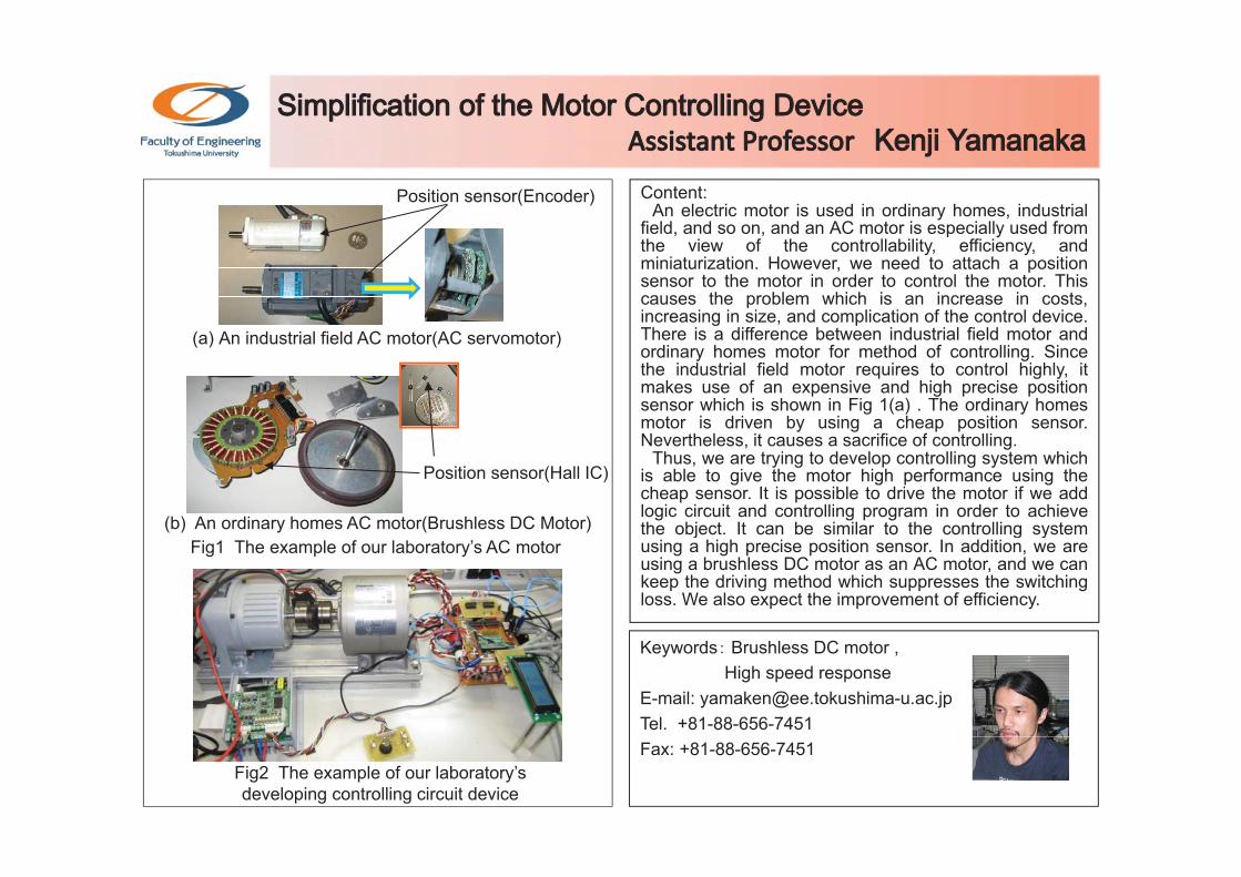
Content:An electric motor is used in ordinary homes, industrial
field, and so on, and an AC motor is especially used fromth i f th t ll bilit ffi i d
Position sensor(Encoder)
the view of the controllability, efficiency, andminiaturization. However, we need to attach a positionsensor to the motor in order to control the motor. Thiscauses the problem which is an increase in costs,increasing in size, and complication of the control device.There is a difference between industrial field motor and(a) An industrial field AC motor(AC servomotor) There is a difference between industrial field motor andordinary homes motor for method of controlling. Sincethe industrial field motor requires to control highly, itmakes use of an expensive and high precise positionsensor which is shown in Fig 1(a) . The ordinary homesmotor is driven by using a cheap position sensor.Nevertheless it causes a sacrifice of controlling
(a) An industrial field AC motor(AC servomotor)
Nevertheless, it causes a sacrifice of controlling.Thus, we are trying to develop controlling system which
is able to give the motor high performance using thecheap sensor. It is possible to drive the motor if we addlogic circuit and controlling program in order to achievethe object. It can be similar to the controlling system
Position sensor(Hall IC)
(b) An ordinary homes AC motor(Brushless DC Motor) j g yusing a high precise position sensor. In addition, we areusing a brushless DC motor as an AC motor, and we cankeep the driving method which suppresses the switchingloss. We also expect the improvement of efficiency.
Fig1 The example of our laboratory’s AC motor
Keywords Brushless DC motor ,High speed response
E-mail: [email protected]. +81-88-656-7451Fax: +81-88-656-7451
Fig2 The example of our laboratory’s developing controlling circuit device