6–12 w dc/dc power modules 24 v input series · 6–12 w dc/dc power modules 24 v input series...
TRANSCRIPT
PKF 2000 I
6–12 W DC/DC Power Modules24 V Input Series
�
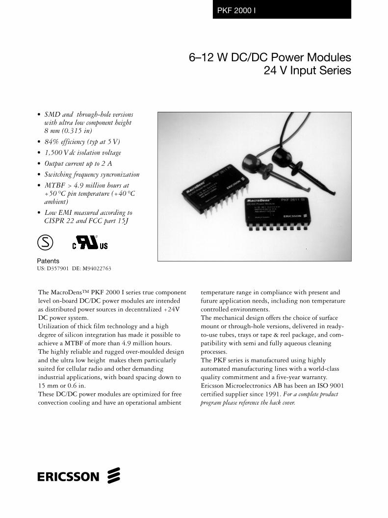
• SMD and through-hole versionswith ultra low component height8 mm (0.315 in)
• 84% efficiency (typ at 5 V)
• 1,500 V dc isolation voltage
• Output current up to 2 A
• Switching frequency syncronization
• MTBF > 4.9 million hours at+50°C pin temperature (+40°Cambient)
• Low EMI measured according toCISPR 22 and FCC part 15J
The MacroDens™ PKF 2000 I series true componentlevel on-board DC/DC power modules are intendedas distributed power sources in decentralized +24VDC power system.Utilization of thick film technology and a highdegree of silicon integration has made it possible toachieve a MTBF of more than 4.9 million hours.The highly reliable and rugged over-moulded designand the ultra low height makes them particularlysuited for cellular radio and other demandingindustrial applications, with board spacing down to15 mm or 0.6 in.These DC/DC power modules are optimized for freeconvection cooling and have an operational ambient
temperature range in compliance with present andfuture application needs, including non temperaturecontrolled environments.The mechanical design offers the choice of surfacemount or through-hole versions, delivered in ready-to-use tubes, trays or tape & reel package, and com-patibility with semi and fully aqueous cleaningprocesses.The PKF series is manufactured using highlyautomated manufacturing lines with a world-classquality commitment and a five-year warranty.Ericsson Microelectronics AB has been an ISO 9001certified supplier since 1991. For a complete productprogram please reference the back cover.
PatentsUS: D357901 DE: M94022763
2 EN/LZT 146 31 R1A (Replaces EN/LZT 137 21 R6) © Ericsson Microelectronics AB, June 2000
General
Absolute Maximum Ratings
Characteristics
Isolation voltage(input to output test voltage)
VISO
Input TC < TCmax unless otherwise specified
mW
mW
Input stand-by powerPRC
min max Unit
TC Case temperature at full output power –45 +100 °C
TS Storage temperature –55 +125 °C
VI Continuous input voltage –0.5 +40 V dc
1,500 V dc
Vtr Transient input energy 0.01 Ws
VRC Remote control voltage pin 10, 11 ref. to pin 18 –5 VI V dc
Vadj Output adjust voltage pin 8, 9 ref. to pin 18 –5 +40 V dc
VI Input voltage range1) 18 36 V
VIoff Turn-off input voltage 16 18 V16.8See typical characteristics
VIon Turn-on input voltage 19 V18.3See typical characteristics
CI Input capacitance �F2.4
PIi Input idling power IO= 0, TC=–30…+85°C(VI=24V)(VI=27V)
360300
(VI=24V)(VI=27V)
2540
TC=–30…+85°C,RC connected to pin 18
Characteristics Conditions min typ max Unit
Stress in excess of Absolute MaximumRatings may cause permanent damage.Absolute Maximum Ratings, sometimesreferred to as no destruction limits, arenormally tested with one parameter at atime exceeding the limits of Output dataor Electrical Characteristics. If exposed tostress above these limits, function andperformance may degrade in an unspeci-fied manner.
NOTES:
1) The power modules will operate down toVI �18 V, when VI decreases, but will turn onat VI �19 V, when VI increases (see alsoOperating Information.
2) The test is applicable for through-holeversions.
Environmental Characteristics
Characteristics
Frequency 10…500 HzAmplitude 0.75 mmAcceleration 10 gNumber of cycles 10 in each axis
Vibration(Sinusoidal)
JESD 22-B103(IEC 68-2-6 Fc)
Test procedure & conditions
Frequency 10…500 HzAcceleration densityspectrum 0.5 g2/HzDuration 10 min in 3 directionsReproducability medium (IEC 62-2-36)
MIL-STD-883Method 2026(IEC 68-2-34 Ed)
Randomvibration
Peak acceleration 200 gShock duration 3 ms
Shock(Half sinus)
JESD 22-B104(IEC 68-2-27 Ea)
Temperature 85°CHumidity 85% RHDuration 1000 hours
Temperature –40°C…+125°CNumber of cycles 500
Temperature, solder 260°CDuration 10…13 s
Temperaturechange
Accelerateddamp heat
Solderresistability2)
JESD 22-A104(IEC 68-2-14 Na)
JESD 22-A101(IEC 68-2-3 Ca
with bias)
JESD 22-B106(IEC 68-2-20 Tb 1A)
Duration 96 hTemperature 35°CConcentration 5 %
IEC 68-2-11 KaAggressiveenvironment
EN/LZT 146 31 R1A (Replaces EN/LZT 137 21 R6) © Ericsson Microelectronics AB, June 2000 3
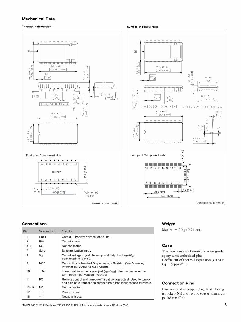
Mechanical Data
Through-hole version
Foot print Component side Foot print Component side
Dimensions in mm (in)
•
• • • • • • • • •
• • • • • • • • •
∅ ×3.6 [0.142]
5.0 [0.197]
24
.0[0
.94
5]
29
.6[1
.16
5]
2.8
[0.1
10
]1 2 3 4 5 6 7 8 9
101112131415161718
40.0 [1.575]
Dimensions in mm (in)
Surface-mount version
�����������
Pin Designation Function
Connections
1 Out 1 Output 1. Positive voltage ref. to Rtn.
2 Rtn Output return.
3–6 NC Not connected.
7 Sync Synchronization input.
8 Vadj Output voltage adjust. To set typical output voltage (VOi)connect pin 8 to pin 9.
9 NOR Connection of Nominal Output voltage Resistor. (See OperatingInformation, Output Voltage Adjust).
10 TOA Turn-on/off input voltage adjust (VIon/VIoff). Used to decrease theturn-on/off input voltage threshold.
11 RC Remote control and turn-on/off input voltage adjust. Used to turn-onand turn-off output and to set the turn-on/off input voltage threshold.
12–16 NC Not connected.
17 +In Positive input.
18 – In Negative input.
CaseThe case consists of semiconductor gradeepoxy with embedded pins.Coefficient of thermal expansion (CTE) istyp. 15 ppm/°C.
WeightMaximum 20 g (0.71 oz).
Connection PinsBase material is copper (Cu), first platingis nickel (Ni) and second (outer) plating ispalladium (Pd).

4 EN/LZT 146 31 R1A (Replaces EN/LZT 137 21 R6) © Ericsson Microelectronics AB, June 2000
Thermal DataTwo-parameter model
This model provides a more precise description of the thermalcharacteristics to be used for thermal calculations.Thermally the power module can be considered as a componentand the case temperature can be used to characterize theproperties. The thermal data for a power module with thesubstrate in contact with the case can be described with twothermal resistances. One from the case to ambient air and onefrom case to PB (Printed Board).The thermal characteristics can be calculated from the followingformula:TPB = (TC–TA)×(Rth C–PB+Rth C–A)/Rth C–A–Pd×Rth C–PB+TAWhere:Pd: dissipated power, calculated as PO ×(l/h–1)TC: max average case temperatureTA: ambient air temperature at the lower side of the power
moduleTPB: temperature in the PB between the PKF connection pinsRth C-PB: thermal resistance from case to PB under the power
moduleRth C-A: thermal resistance from case to ambient airv: velocity of ambient air.Rth C-PB is constant and Rth C-A is dependent on the air velocity.
Free convection is equal to an air velocity of approx.0.2 – 0.3 m/s. See figure below.
Palladium plating is used on the terminal pins. A pin tem-perature(Tp) in excess of the solder fusing temperature (+183°C for Sn/Pb63/37) for more than 25 seconds and a peak temperature above195°C, is required to guarantee a reliable solder joint.Both pin 1 and pin 9 must be monitored.No responsibility is assumed if these recommendations arenot strictly followed.
Reflow Soldering InformationThe PKF series of DC/DC power modules are manufactured insurface mount technology. Extra precautions must therefore betaken when reflow soldering the surface mount version. Neglec-ting the soldering information given below may result in perma-nent damage or significant degradation of power module per-formance.The PKF series can be reflow soldered using IR, NaturalConvection, Forced Convection or Combined IR/ConvectionTechnologies. The high thermal mass of the component and itseffect on �T (°C) requires that particular attention be paid toother temperature sensitive components.IR Reflow technology may require the overall profile time to beextended to approximately 8–10 minutes to ensure an acceptable�T. Higher activity flux may be more suitable to overcome theincrease in oxidation and to avoid flux burn-up.The general profile parameters detailed in the diagram, with thisex-tended time to reach peak temperatures, would then besuitable.Note! These are maximum parameters. Depending on processvariations, an appropriate margin must be added.
EN/LZT 146 31 R1A (Replaces EN/LZT 137 21 R6) © Ericsson Microelectronics AB, June 2000 5
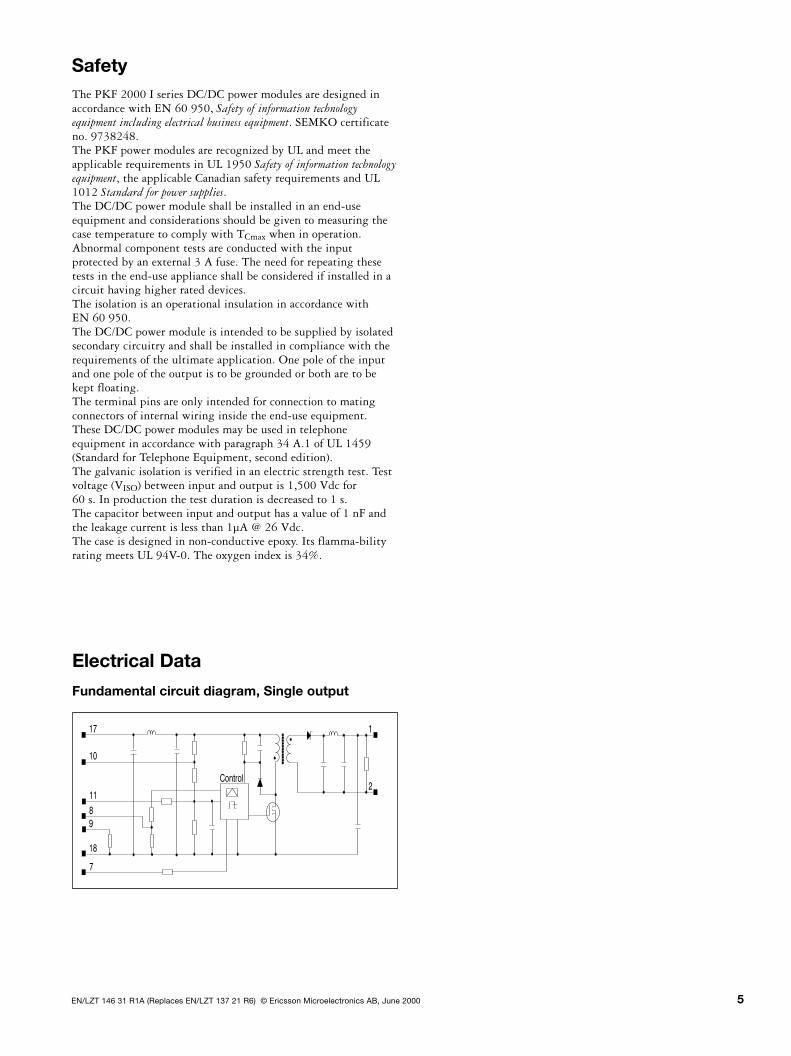
Electrical Data
Fundamental circuit diagram, Single output
Control
1
2
17
10
11
18
7
9
8
SafetyThe PKF 2000 I series DC/DC power modules are designed inaccordance with EN 60 950, Safety of information technologyequipment including electrical business equipment. SEMKO certificateno. 9738248.The PKF power modules are recognized by UL and meet theapplicable requirements in UL 1950 Safety of information technologyequipment, the applicable Canadian safety requirements and UL1012 Standard for power supplies.The DC/DC power module shall be installed in an end-useequipment and considerations should be given to measuring thecase temperature to comply with TCmax when in operation.Abnormal component tests are conducted with the inputprotected by an external 3 A fuse. The need for repeating thesetests in the end-use appliance shall be considered if installed in acircuit having higher rated devices.The isolation is an operational insulation in accordance withEN 60 950.The DC/DC power module is intended to be supplied by isolatedsecondary circuitry and shall be installed in compliance with therequirements of the ultimate application. One pole of the inputand one pole of the output is to be grounded or both are to bekept floating.The terminal pins are only intended for connection to matingconnectors of internal wiring inside the end-use equipment.These DC/DC power modules may be used in telephoneequipment in accordance with paragraph 34 A.1 of UL 1459(Standard for Telephone Equipment, second edition).The galvanic isolation is verified in an electric strength test. Testvoltage (VISO) between input and output is 1,500 Vdc for60 s. In production the test duration is decreased to 1 s.The capacitor between input and output has a value of 1 nF andthe leakage current is less than 1µA @ 26 Vdc.The case is designed in non-conductive epoxy. Its flamma-bilityrating meets UL 94V-0. The oxygen index is 34%.
6 EN/LZT 146 31 R1A (Replaces EN/LZT 137 21 R6) © Ericsson Microelectronics AB, June 2000
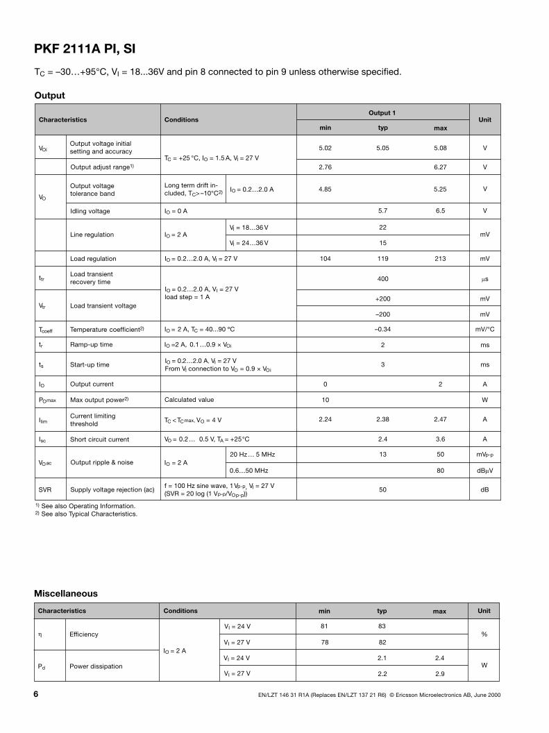
PKF 2111A PI, SI
TC = –30…+95°C, VI = 18...36V and pin 8 connected to pin 9 unless otherwise specified.
0 2 A
Characteristics ConditionsOutput 1
min typ maxUnit
Output voltage initialsetting and accuracyVOi
Output voltagetolerance bandVO
IO = 0 A
Load regulation
ttr
Load transient voltageVtr
Temperature coefficient2)Tcoeff
Ramp-up timetr
Start-up timets
Output currentIO
Max output power2)POmax
Current limitingthreshold
Ilim TC <TCmax, VO = 4 V
Short circuit currentIsc VO = 0.2… 0.5 V, TA = +25°C
20 Hz… 5 MHz
Line regulation IO = 2 A
Load transientrecovery time
5.02 5.05 5.08 V
5.7 6.5 V
mV
104 119 213 mV
+200 mV
–200 mV
IO = 2 A, TC = 40...90 ºC –0.34 mV/°C
2 ms
3 ms
10 W
2.24 2.38 2.47 A
2.4 3.6 A
13 50 mVp-p
80 dB�V
400 �s
0.6…50 MHz
Long term drift in-cluded, TC>–10°C2)
Output
VI = 18…36 V
VI = 24…36 V 15
22
Output adjust range1) 2.76 6.27 V
4.85 5.25IO = 0.2…2.0 A
VOac Output ripple & noise IO = 2 A
f = 100 Hz sine wave, 1Vp-p, VI = 27 V(SVR = 20 log (1 Vp-p/VOp-p))
TC = +25 °C, IO = 1.5 A, VI = 27 V
IO =2 A, 0.1…0.9 × VOi
1) See also Operating Information.2) See also Typical Characteristics.
SVR Supply voltage rejection (ac)
IO = 0.2…2.0 A, VI = 27 VFrom VI connection to VO = 0.9 × VOi
IO = 0.2…2.0 A, VI = 27 V
IO = 0.2…2.0 A, VI = 27 Vload step = 1 A
50 dB
Idling voltage
Calculated value
V
2.1 2.4
Characteristics Conditions Unitmin typ max
Pd Power dissipation
Miscellaneous
%Efficiency�
IO = 2 A
81 83
VI = 24 V
VI = 27 V
VI = 24 V
VI = 27 V 78 82
2.2 2.9W
EN/LZT 146 31 R1A (Replaces EN/LZT 137 21 R6) © Ericsson Microelectronics AB, June 2000 7
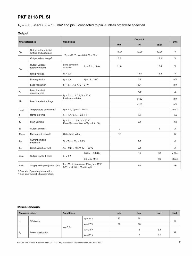
PKF 2113 PI, SI
TC = –30…+95°C, VI = 18...36V and pin 8 connected to pin 9 unless otherwise specified.
Output
2 2.5
Characteristics Conditions Unitmin typ max
Pd Power dissipation
Miscellaneous
%Efficiency�
IO = 1 A
83 86
VI = 24 V
VI = 27 V
VI = 24 V
VI = 27 V 83 86
2 2.5W
0 1 A
Characteristics ConditionsOutput 1
min typ maxUnit
Output voltage initialsetting and accuracyVOi
Output voltagetolerance bandVO
IO = 0 A
Load regulation
ttr
Load transient voltageVtr
Temperature coefficient2)Tcoeff
Ramp-up timetr
Start-up timets
Output currentIO
Max output power2)POmax
Current limitingthreshold
Ilim TC <TCmax, VO = 9.6 V
Short circuit currentIsc VO = 0.2… 0.5 V, TA = +25°C
20 Hz… 5 MHz
Line regulation IO = 1 A
Load transientrecovery time
11.94 12.00 12.06 V
13.4 16.3 V
224 mV
+120 mV
–120 mV
IO = 1 A, TC = 40...90 ºC 0 mV/°C
2.3 ms
3.1 ms
12 W
1.4 A
2.1 A
15 50 mVp-p
80 dB�V
760 �s
0.6…50 MHz
Long term driftincluded
VI = 18…36 V 33 mV
Output adjust range1) 6.5 15.0 V
11.6 12.6 VIO = 0.1…1.0 A
VO ac Output ripple & noise IO = 1 A
f = 100 Hz sine wave, 1 Vp-p, VI = 27 V(SVR = 20 log (1 Vp-p/VOp-p))
TC = +25 °C, IO = 0.8A, VI = 27 V
IO = 1 A, 0.1… 0.9 × VOi
1) See also Operating Information.2) See also Typical Characteristics.
SVR Supply voltage rejection (ac)
IO = 0.1… 1.0 A, VI = 27 VFrom VI connection to VO = 0.9 × VOi
IO = 0.1…1.0 A, VI = 27 V
IO = 0.1… 1.0 A, VI = 27 Vload step = 0.5 A
50 dB
Idling voltage
Calculated value

8 EN/LZT 146 31 R1A (Replaces EN/LZT 137 21 R6) © Ericsson Microelectronics AB, June 2000
PKF 2610A PI, SI
TC = –30…+95°C, VI = 18...36V and pin 8 connected to pin 9 unless otherwise specified.
0 2 A
Characteristics ConditionsOutput 1
min typ maxUnit
Output voltage initialsetting and accuracyVOi
Output voltagetolerance bandVO
IO = 0 A
Load regulation
ttr
Load transient voltageVtr
Temperature coefficient2)Tcoeff
Ramp-up timetr
Start-up timets
Output currentIO
Max output power2)POmax
Current limitingthreshold
Ilim TC <TCmax
Short circuit currentIsc VO = 0.2… 0.5 V, TA = +25°C
20 Hz… 5 MHz
Line regulation IO = 2 A
Load transientrecovery time
3.27 3.30 3.33 V
3.8 4.0 V
mV
120 mV
+180 mV
–180 mV
IO = 2 A, TC = 40...90 ºC -0.55 mV/°C
2.3 ms
4.4 ms
6.6 W
2.2 2.6 A
2.9 A
15 50 mVp-p
80 dB�V
100 �s
20 Hz…50 MHz
Long term driftincluded
Output
VI = 18…36 V
VI = 27…36 V 35
50
Output adjust range1) 1.80 3.80 V
3.17 3.43IO = 0.2…2.0 A
VOac Output ripple & noise IO = 2 A
f = 100 Hz sine wave, 1Vp-p, VI = 27 V(SVR = 20 log (1 Vp-p/VOp-p))
TC = +25 °C, IO = 1.0 A, VI = 27 V
IO = 2 A, 0.1… 0.9 × VOi
1) See also Operating Information.2) See also Typical Characteristics.
SVR Supply voltage rejection (ac)
IO = 0.2…2.0 A, VI = 27 VFrom VI connection to VO = 0.9 × VOi
IO = 0.2…2.0 A, VI = 27 V
IO = 0.2…2.0 A, VI = 27 Vload step = 1 A
63 dB
Idling voltage
Characteristics Conditions Unitmin typ max
Efficiency�
Miscellaneous
Pd Power dissipation
IO = 2 A, VI = 27 V
IO = 2 A, VI = 27 V 1.6 2.1 W
76 81 %
Calculated value
V

EN/LZT 146 31 R1A (Replaces EN/LZT 137 21 R6) © Ericsson Microelectronics AB, June 2000 9
PKF 2611 PI, SI
TC = –30…+95°C, VI = 18...36V and pin 8 connected to pin 9 unless otherwise specified.
0 1.2 A
Characteristics ConditionsOutput 1
min typ maxUnit
Output voltage initialsetting and accuracyVOi
Output voltagetolerance bandVO
IO = 0 A
Load regulation
ttr
Load transient voltageVtr
Temperature coefficient2)Tcoeff
Ramp-up timetr
Start-up timets
Output currentIO
Max output power2)POmax
Current limitingthreshold
Ilim TC <TCmax
Short circuit currentIsc VO = 0.2… 0.5 V, TA = +25°C
20 Hz… 5 MHz
Line regulation IO = 1.2 A
Load transientrecovery time
5.02 5.05 5.08 V
5.8 V
mV
125 mV
+100 mV
–100 mV
IO = 1.2 A, TC = 40...90 ºC -0.8 mV/°C
2.3 ms
4.6 ms
6 W
1.3 1.6 2.4 A
2.0 A
20 70 mVp-p
80 dB�V
50 �s
20 Hz…50 MHz
Long term driftincluded
Output
VI = 18…36 V
VI = 27…36 V 10
30
Output adjust range1) 4.30 5.80 V
4.85 5.25 VIO = 0.12…1.2 A
VOac Output ripple & noise IO = 1.2 A
f = 100 Hz sine wave, 1Vp-p, VI = 27 V(SVR = 20 log (1 Vp-p/VOp-p))
TC = +25 °C, IO = 0.5 A, VI = 27 V
IO = 1.2 A, 0.1… 0.9 × VOi
1) See also Operating Information.2) See also Typical Characteristics.
SVR Supply voltage rejection (ac)
IO = 0.12…1.2 A, VI = 27 VFrom VI connection to VO = 0.9 × VOi
IO = 0.12…1.2 A, VI = 27 V
IO = 0.12…1.2 A, VI = 27 Vload step = 0.6 A
60 dB
Idling voltage
Characteristics Conditions Unitmin typ max
Efficiency�
Miscellaneous
Pd Power dissipation
IO = 1.2 A, VI = 27 V
IO = 1.2 A, VI = 27 V 1.2 1.6 W
79 83 %
Calculated value
10 EN/LZT 146 31 R1A (Replaces EN/LZT 137 21 R6) © Ericsson Microelectronics AB, June 2000
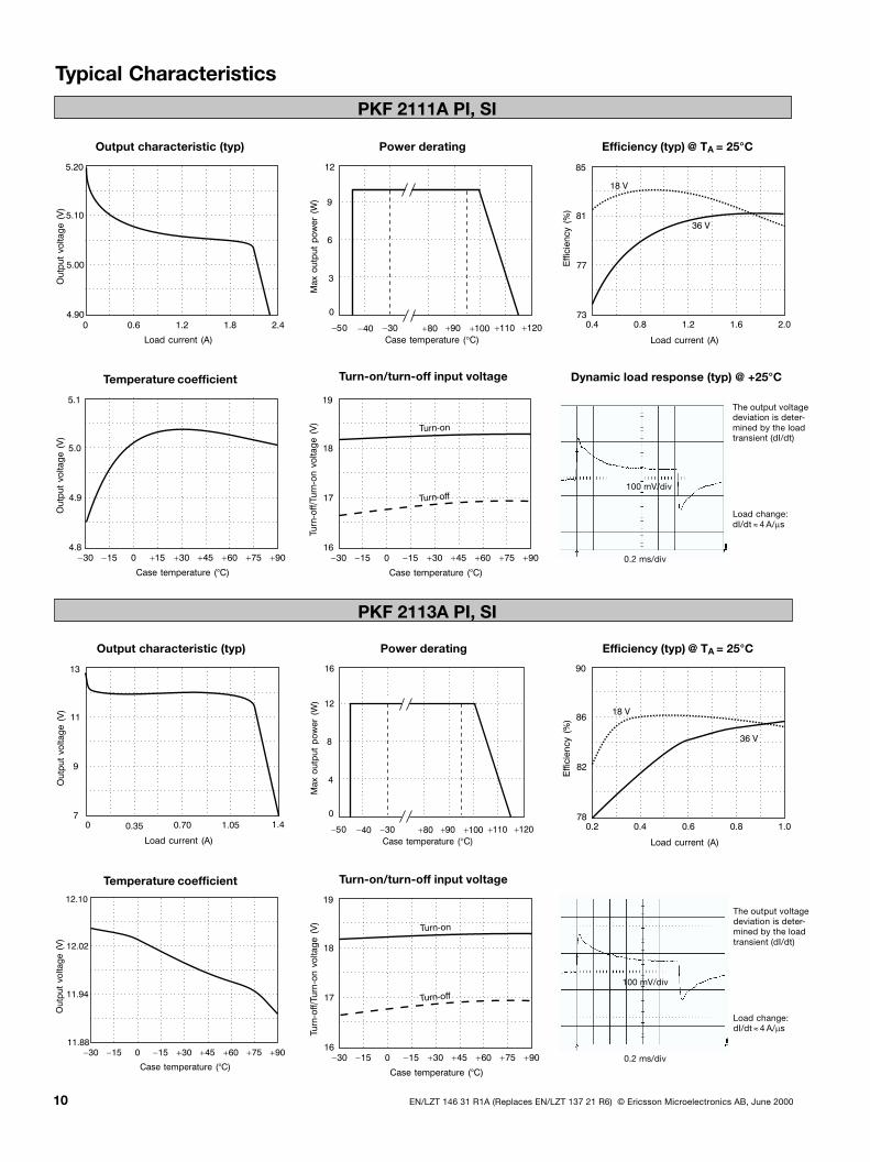
Typical Characteristics
PKF 2111A PI, SI
Output characteristic (typ) Power derating
Temperature coefficient Turn-on/turn-off input voltage
Efficiency (typ) @ TA = 25°C
Temperature coefficient Turn-on/turn-off input voltage
Output characteristic (typ) Power derating Efficiency (typ) @ TA = 25°C
PKF 2113A PI, SI
Dynamic load response (typ) @ +25°C
0.2 ms/div
100 mV/div
0.2 ms/div
100 mV/div
The output voltagedeviation is deter-mined by the loadtransient (dI/dt)
Load change:dI/dt � 4 A/�s
The output voltagedeviation is deter-mined by the loadtransient (dI/dt)
Load change:dI/dt � 4 A/�s
EN/LZT 146 31 R1A (Replaces EN/LZT 137 21 R6) © Ericsson Microelectronics AB, June 2000 11
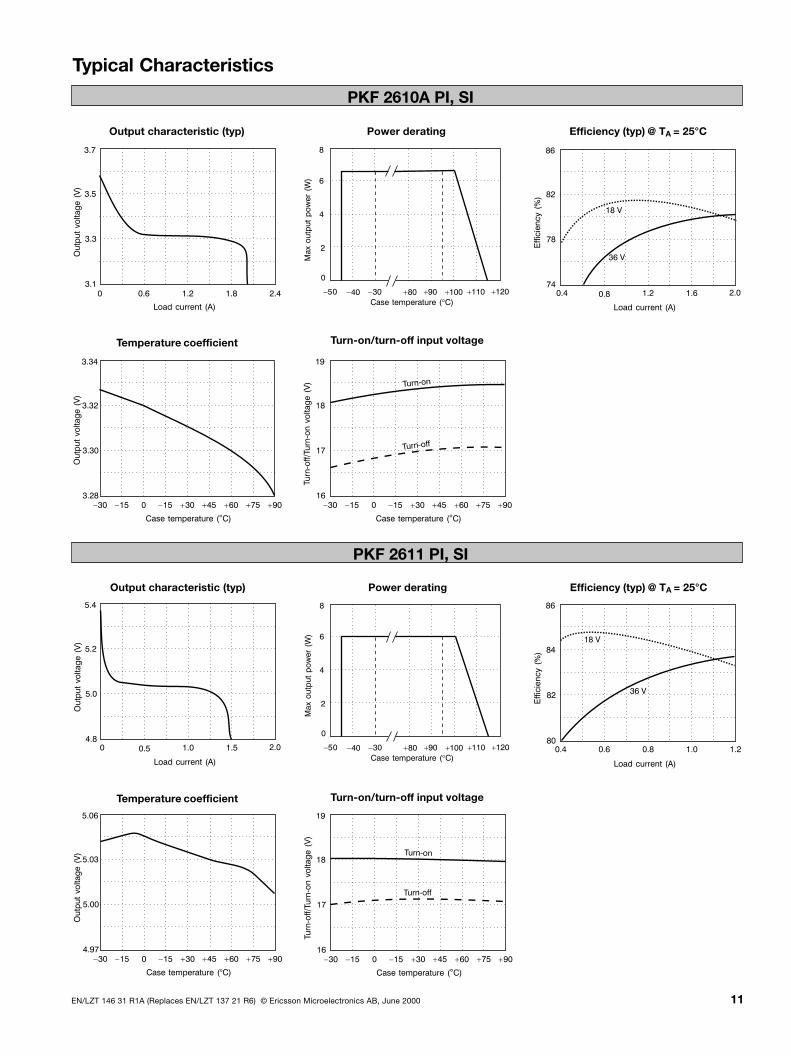
Typical Characteristics
PKF 2610A PI, SI
Output characteristic (typ) Power derating
Temperature coefficient Turn-on/turn-off input voltage
Efficiency (typ) @ TA = 25°C
Temperature coefficient Turn-on/turn-off input voltage
Output characteristic (typ) Power derating Efficiency (typ) @ TA = 25°C
80
82
84
86
0.4 0.6 0.8 1.0 1.2
Load current (A)
Effic
ien
cy
(%)
18 V
36 V
PKF 2611 PI, SI
12 EN/LZT 146 31 R1A (Replaces EN/LZT 137 21 R6) © Ericsson Microelectronics AB, June 2000
EMC Specifications
The fundamental switching frequency is 510 kHz ±10 kHz.
The signal is amplitude modulated with 1 kHz/80% and applied indifferential and common mode.
Radiated EMS (Electro-Magnetic Fields)
Radiated EMS is measured according to test methods inIEC Standard publ. 801-3. No deviation outside the VO toleranceband will occur under the following conditions:
Frequency range Voltage level0.01...200 MHz 3 Vrms/m200...1,000 MHz 3 Vrms/m1...12 GHz 10 Vrms/m
ESD
Electro Static Discharge is tested according to IEC publ. 801-2. Nodestruction will occur if the following voltage levels are applied toany of the terminal pins:
Test Voltage levelAir discharge ±4 kVContact discharge ±2 kV
EFT
Electrical Fast Transients on the input terminals could affect the out-put voltage regulation causing functional errors on the Printed BoardAssembly (PBA). The PKF power module withstand EFT levels of0.5 kV keeping VO within the tolerance band and2.0 kV without destruction. Tested according to IEC publ. 801-4.
Output Ripple & Noise (VOac)
Output ripple is measured as the peak to peak voltage of the funda-mental switching frequency.
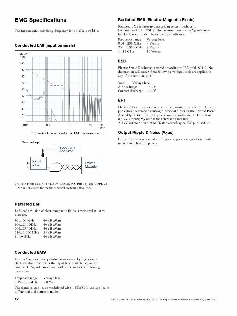
Conducted EMI (input teminals)
PKF series typical conducted EMI performance
Test set up
The PKF meets class A in VDE 0871/0878, FCC Part 15J, and CISPR 22(EN 55022), except for the fundamental switching frequency.
Radiated EMI
Radiated emission of electromagnetic fields is measured at 10 mdistance.
30...100 MHz 60 dB �V/m100...200 MHz 40 dB �V/m200...230 MHz 30 dB �V/m230...1,000 MHz 35 dB �V/m1...10 GHz 46 dB �V/m
Frequency range Voltage level0.15...300 MHz 1.0 Vrms
Conducted EMS
Electro Magnetic Susceptibility is measured by injection ofelectrical disturbances on the input terminals. No deviationoutside the VO tolerance band will occur under the followingconditions:

EN/LZT 146 31 R1A (Replaces EN/LZT 137 21 R6) © Ericsson Microelectronics AB, June 2000 13
Operating Information
Over Voltage Protection (OVP)The remote control can be utilized also for OVP by using the ex-ternal circuitry in figure 2. Resistor values are for 5V output app-lications, but can easily be adjusted for other output voltages andthe desired OVP level.
Remote Control (RC)Turn-on or turn-off can be realized by using the RC-pin. Normaloperation is achieved if pin 11 is open (NC). If pin 11 is con-nected to pin 18 the power module turns off. To ensure safe turn-off the voltage difference between pin 11 and 18 shall be less than1.0V. RC is an TTL open collector compatible output with a sinkcapacity >300 mA (see fig. 1).
Figure 1
Figure 2
Rtn (pin 2) �In (pin 18)
Out 1 (pin 1)
RC (pin 11)
15k 1.2k
1k
TL431
10k270
V , NOR (pin 8, 9)adj
–In (pin 18)
Radj
Increase VO
NOR (pin 9)
V (pin 8)adj
Radj
Decrease VO
Figure 4
RC (pin 11)
−In (pin 18)
RIon
Increase VIon
RC (pin 11)
TOA (pin 10)
RIon
Decrease VIon
Figure 3
Fuse ConsiderationsTo prevent excessive current from flowing through the inputsupply line, in the case of a short-circuit across the converter in-put, an external fuse should be installed in the non-earthed inputsupply line. We recommend using a fuse rated at approximately2 to 4 times the value calculated in the formula below:
Refer to the fuse manufacturer for further information.
Output Voltage Adjust (Vadj)
Output voltage, VO, can be adjusted by using an external resistor.Typical adjust range is ±15%. If pin 8 and 9 is not connected to-gether the output will decrease to a low value. To increase VO aresistor should be connected between pin 8/9 and 18, and todecrease VO a resistor should be connected between pin 8 and 9(see fig. 4).
Typical required resistor value to increase VO is given by:
Radj = k5 × (k6 – VO)/(VO – VOi) kW
where VO is the desired output voltage,VOi is the typical output voltage initial setting
and k5= 4.2 k6= 6.27 V PKF 2111Ak5= 4.2 k6= 15.0 V PKF 2113A
k5= 3.18 k6= 3.90V PKF 2610Ak5= 3.18 k6= 5.85V PKF 2611
Typical required resistor value to decrease VO is given by:
Radj = k7 × (VOi – VO)/(VO – k8) kW
where k7= 18.0 k8= 2.76 V PKF 2111Ak7= 18.6 k8= 6.50 V PKF 2113Ak7= 17.2 k8= 1.70 V PKF 2610Ak7= 12.5 k8= 4.28 V PKF 2611
Turn-on/off Input VoltageThe power module monitors the input voltage and will turn onand off at predetermined levels. The typical turn-on level (with-out any external resistor) is 18.4 V and the typical turn-off level is17.0 V, a slight deviation can occur due to tolerances in themanufacturing process. These levels can be adjusted by means ofexternal resistors.
k1 k2 k3 k41020 18.3 22 16.9 PKF 2111A, PKF 2113A1020 18.4 27 17.0 PKF 2610A1020 18.4 25 17.0 PKF 2611
Turn-off level. VIoff is the adjusted turn-off level and is deter-mined by the following equation: VIoff = VIon – 1.5V (typicalvalue).
To increase VIon a resistor should be connected between pin 11and 18 (see fig. 3).
The resistance is given by the following equation(For VIon>18.4V):
RIon = (k1 – VIon)/(VIon – k2) kW
where k2 is the typical unadjusted turn-on input voltage (V).
To decrease VIon a resistor should be connected between pin 10and 11 (see fig. 3). The resistance is given by the followingequation (for 17.0V < VIon >18.3V:
RIon = k3 × (VIon – k4)/(k2 – VIon) kWPOmax
(�min × VImin)Iinmax =
14 EN/LZT 146 31 R1A (Replaces EN/LZT 137 21 R6) © Ericsson Microelectronics AB, June 2000
Capacitive LoadThe PKF series has no maximum limit for capacitive load on theoutput. The power module may operate in current limiting modeduring start-up, affecting the ramp-up and the start-up time. Foroptimum start performance we recommend maximum 100 �F/Aof IO. Connect capacitors at the point of load for best perfor-mance.
Input and Output ImpedanceBoth the source impedance of the power feeding and the load im-pedance will interact with the impedance of the DC/DC powermodule.
It is most important to have the ratio between L and C as lowas possible, i.e. a low characteristic impedance, both at the inputand output, as the power modules have a low energy storagecapability.
Use an electrolytic capacitor across the input if the sourceinductance is larger than 10��H. Their equivalent series resist-ance together with the capacitance acts as a lossless damping fil-ter. Suitable capacitor values are in the range 10–100 �F.
Current Limiting Protection (Ilim)The output power is limited at loads above the output currentlimiting threshold (Ilim), specified as a minimum value.
Parallel OperationParalleling of several converters is easily accomplished by directconnection of the output voltage terminal pins. The load regula-tion characteristic is specifically designed for optimal parallelingperformance. Load sharing between converters will be within±10%. It is recommended not to exceed PO = n × 0.9 × POmax,where POmax is the maximum converter output power and n thenumber of paralleled converters, to prevent overloading any of theconverters and thereby decreasing the reliability performance.
Synchronization (Sync)It is possible to synchronize the switching frequency to anexternal symmetrical clock signal. The input is TTL-compatibleand referenced to the input pin 18.
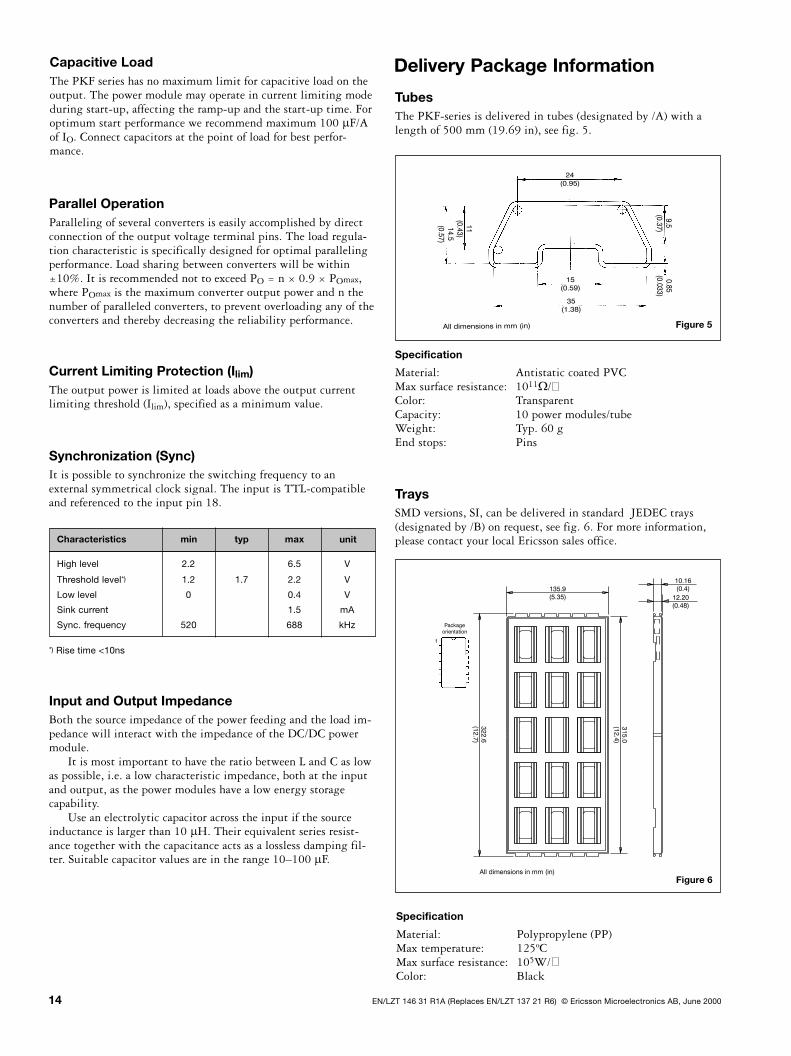
Delivery Package Information
TubesThe PKF-series is delivered in tubes (designated by /A) with alength of 500 mm (19.69 in), see fig. 5.
Figure 5
TraysSMD versions, SI, can be delivered in standard JEDEC trays(designated by /B) on request, see fig. 6. For more information,please contact your local Ericsson sales office.
Figure 6
High level 2.2 6.5 V
Threshold level*) 1.2 1.7 2.2 V
Low level 0 0.4 V
Sink current 1.5 mA
Sync. frequency 520 688 kHz
*) Rise time <10ns
Characteristics min typ max unit
Specification
Material: Antistatic coated PVCMax surface resistance: 1011�/Color: TransparentCapacity: 10 power modules/tubeWeight: Typ. 60 gEnd stops: Pins
Specification
Material: Polypropylene (PP)Max temperature: 125ºCMax surface resistance: 105W/Color: Black

EN/LZT 146 31 R1A (Replaces EN/LZT 137 21 R6) © Ericsson Microelectronics AB, June 2000 15
Quality
ReliabilityMeantime between failure (MTBF) is calculated to >4.9 millionhours at full output power and a pin temperature of +50°C(TA = +40°C), using the Ericsson failure rate data system.The Ericsson failure rate data system is based on field failurerates and is continously updated. The data corresponds to actualfailure rates of components used in Information Technology andTelecom equipment in temperature controlled environments(TA = –5… +65°C). The data is considered to have a confidencelevel of 90%. For more information see Design Note 002.
Tape & ReelSMD versions, SI, can be delivered in standard tape & reel pack-age (designated by /C) on request, see fig. 7. For more informa-tion, please contact your local Ericsson sales office.
Capacity: 15 power modules/trayStacking pitch: 10.16 mmWeight: Typ. 130 gMin. order quantity: 150 pcs (one box contains 10 full trays)
Figure 7
Specification
Tape material: Conductive polystyrene (PS)Tape width: 72 mmTape pitch: 36 mmMax surface resistance: 105W/Tape color: BlackCover tape color: TransparentReel diameter: 13"Reel hub diameter: 7"Reel capacity: 150 power modules/reelFull reel weight: Typ. 3.7 kgMin. order quantity: 300 pcs (one box contains two reels)
Quality StatementThe products are designed and manufactured in an industrial en-vironment where quality systems and methods like ISO 9000, 6sand SPC, are intensively in use to boost the continuous improve-ments strategy. Infant mortality or early failures in the productsare screened out by a burn-in procedure and an ATE-based finaltest.
Conservative design rules, design reviews and product qualifi-cations, plus the high competence of an engaged work force, con-tribute to the high quality of our products.
WarrantyEricsson Microelectronics warrants to the original purchaser orend user that the products conform to this Data Sheet and are freefrom material and workmanship defects for a period of five (5)years from the date of manufacture, if the product is used withinspecified conditions and not opened. In case the product is dis-continued, claims will be accepted up to three (3) years from thedate of the discontinuation.
For additional details on this limited warranty please refer toEricsson Microelectronics AB’s “General Terms and Conditions ofSales”, or individual contract documents.
Limitation of liabilityEricsson Microelectronics does not make any other warranties, ex-pressed or implied including any warranty of merchantability orfitness for a particular purpose (including, but not limited to, usein life support applications, where malfunctions of product cancause injury to a person’s health or life).
Information given in this data sheet is believed to be accurate and reliable. Noresponsibility is assumed for the consequences of its use nor for any infringementof patents or other rights of third parties which may result from its use.No license is granted by implication or otherwise under any patent or patent rightsof Ericsson Microelectronics. These products are sold only according to EricssonMicroelectronics’ general conditions of sale, unless otherwise confirmed in writing.
Specifications subject to change without notice.
EN/LZT 146 31 R1A (Replaces EN/LZT 137 21 R6)© Ericsson Microelectronics AB, June 2000
*) See also Delivery Package Information
Product Program
VO/IO max Ordering No.*)
PKF 2111A PIPKF 2113A PIPKF 2610A PIPKF 2611A PI
PKF 2111A SIPKF 2113A SIPKF 2610A SIPKF 2611A SI
Output 1
VI PO max
Through-hole SMD
10 W12 W6.6 W6.0 W
5 V/2.0 A12 V/1.0 A3.3 V/2.0 A0.5 V/1.2 A
24 V
Data Sheet
The latest and most complete infor-mation can be found on our website!
Ericsson Microelectronics ABSE-164 81 KISTA, SwedenPhone: +46 8 757 5000www.ericsson.com/microelectronics
For local sales contacts, please refer to our websiteor call: Int. +46 8 757 4700, Fax: +46 8 757 4776