6.004 computation structures spring 2009 for information ... · 3 table of contents binary ..... 4...
TRANSCRIPT

MIT OpenCourseWarehttp://ocw.mit.edu
6.004 Computation Structures Spring 2009
For information about citing these materials or our Terms of Use, visit: http://ocw.mit.edu/terms.

1
A Student’s Guide
to the Digital World
by Margaret Chong

2
Special thanks go out to my best friends in the world – Joe and Bonnie. Where
would I be without your support and hugs. =)
Thank you Professor Terman and Professor Ward for giving me the opportunity
to teach and realize one of my true passions.
Acknowledgements
3
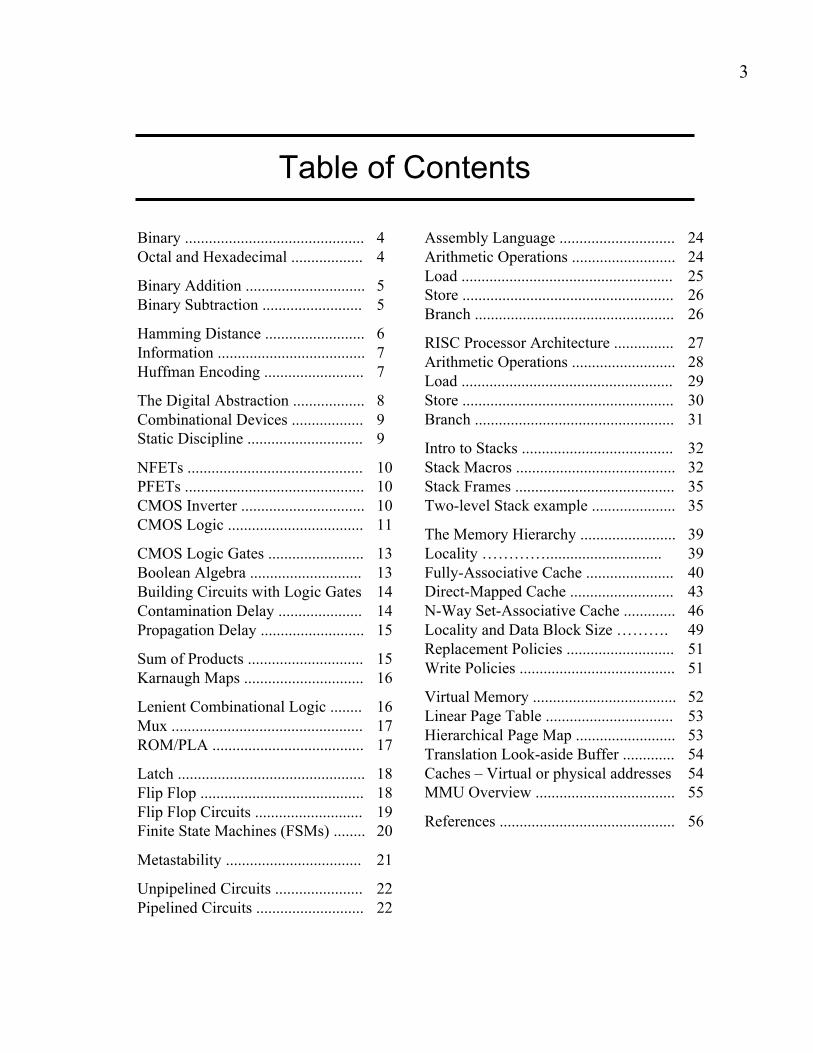
Table of Contents
Binary ............................................. 4 Assembly Language ............................. 24
Octal and Hexadecimal .................. 4 Arithmetic Operations .......................... 24
Load ..................................................... 25Binary Addition .............................. 5
Store ..................................................... 26Binary Subtraction ......................... 5
Branch .................................................. 26
Hamming Distance ......................... 6RISC Processor Architecture ............... 27
Information ..................................... 7Arithmetic Operations .......................... 28
Huffman Encoding ......................... 7Load ..................................................... 29
The Digital Abstraction .................. 8 Store ..................................................... 30
Combinational Devices .................. 9 Branch .................................................. 31
Static Discipline ............................. 9Intro to Stacks ...................................... 32
NFETs ............................................ 10 Stack Macros ........................................ 32
PFETs ............................................. 10 Stack Frames ........................................ 35
CMOS Inverter ............................... 10 Two-level Stack example ..................... 35
CMOS Logic .................................. 11The Memory Hierarchy ........................ 39
CMOS Logic Gates ........................ 13 Locality …………............................. 39
Boolean Algebra ............................ 13 Fully-Associative Cache ...................... 40
Building Circuits with Logic Gates 14 Direct-Mapped Cache .......................... 43
Contamination Delay ..................... 14 N-Way Set-Associative Cache ............. 46
Propagation Delay .......................... 15 Locality and Data Block Size ………. 49
Replacement Policies ........................... 51Sum of Products ............................. 15
Write Policies ....................................... 51Karnaugh Maps .............................. 16
Virtual Memory .................................... 52Lenient Combinational Logic ........ 16
Linear Page Table ................................ 53Mux ................................................ 17
Hierarchical Page Map ......................... 53ROM/PLA ...................................... 17
Translation Look-aside Buffer ............. 54
Latch ............................................... 18 Caches – Virtual or physical addresses 54
Flip Flop ......................................... 18 MMU Overview ................................... 55
Flip Flop Circuits ........................... 19References ............................................ 56
Finite State Machines (FSMs) ........ 20
Metastability .................................. 21
Unpipelined Circuits ...................... 22
Pipelined Circuits ........................... 22
4
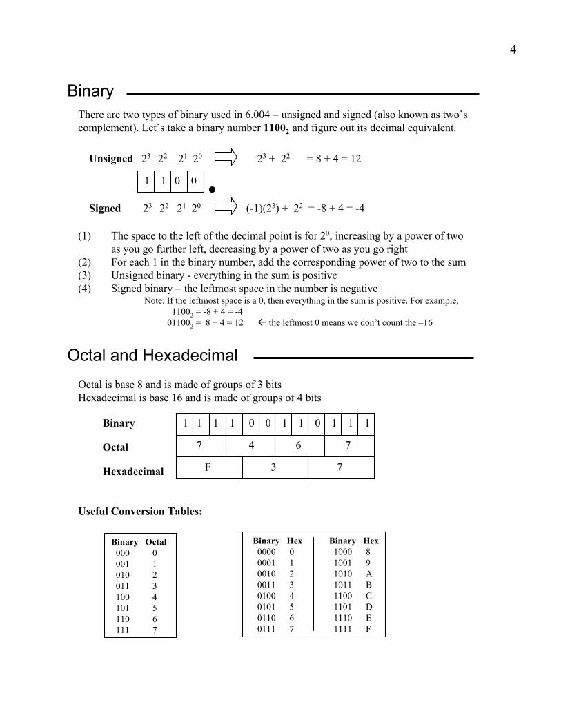
Binary
1 1 0 0
There are two types of binary used in 6.004 – unsigned and signed (also known as two’s
complement). Let’s take a binary number 11002 and figure out its decimal equivalent.
Unsigned 23 22 21 20 23 + 22 = 8 + 4 = 12
Signed 23 22 21 20 (-1)(23) + 22 = -8 + 4 = -4
(1) The space to the left of the decimal point is for 20, increasing by a power of two
as you go further left, decreasing by a power of two as you go right
(2) For each 1 in the binary number, add the corresponding power of two to the sum
(3) Unsigned binary - everything in the sum is positive
(4) Signed binary – the leftmost space in the number is negativeNote: If the leftmost space is a 0, then everything in the sum is positive. For example,
1100 = -8 + 4 = -42
01100 = 8 + 4 = 12 ! the leftmost 0 means we don’t count the –162
Octal and Hexadecimal
Octal is base 8 and is made of groups of 3 bits
Hexadecimal is base 16 and is made of groups of 4 bits
1 1 1 1 0 0 1 1 0 1 1 1
7 4 6 7
F 3 7
Binary
Octal
Hexadecimal
Binary Octal
000 0
001 1
010 2
011 3
100 4
101 5
110 6
111 7
Binary Hex Binary Hex
0000 0 1000 8
0001 1 1001 9
0010 2 1010 A
0011 3 1011 B
0100 4 1100 C
0101 5 1101 D
0110 6 1110 E
0111 7 1111 F
Useful Conversion Tables:
5
Signed Binary Addition
Binary addition is the same as regular addition, except you only have 0’s and 1’s.
3
+ 5
8
1
00011
+ 00101
0
11
00011
+ 00101
00
111
00011
+ 00101
000
111
00011
+ 00101
1000
111
00011
+ 00101
01000
1+1 = 2 = 10 in binary, so carry the 1
Most machines have a fixed number of bits. In the example above, the operands are both
5 bits wide, therefore the result can only be expressed in 5 bits. This introduces the
possibility that the sum might be incorrect.
3
+ 5
??
1
0011
+ 0101
0
11
0011
+ 0101
00
111
0011
+ 0101
000
111
0011
+ 0101
1000
-8 is incorrect!
We cannot express 8
in four bits
-8
+ -8
??
1000
+ 1000
1 0 is incorrect! 1000
+ 1000 We cannot express –16 in four bits 0000
Let’s do this by example, say we’re subtracting 3 minus 5
(1) Represent 3 and 5 in binary
(2) Figure out the binary representation for negative 5 by flipping the bits and adding one
(3) Compute 3 plus negative 5
3
- 5
-2
3 = 000111
5 = 00101
3 = 000112
-5 = 11010
+ 00001
11011
11
000113
+ 11011
Signed Binary Subtraction
11110
Note that, like in binary addition, we are constrained to a fixed number of bits. Therefore,
you might encounter cases where the “flip the bits and add one” cannot be represented in
some fixed number of bits. You may also find that the result cannot be represented in
some fixed number of bits.

6
Hamming Distance
One factor to consider when transmitting a message is the possibility that the message
might get corrupted in transit. For example, say we’re transmitting the outcome of a coin
flip over the internet. There are two possible outcomes – heads or tails.
One possible encoding uses only one bit: heads = “0” and tails = “1”. We tell our friend
that the coin flipped heads by transmitting a “0.” However, a routing wire is struck
by lightning, changing the bit to a “1.” Our friend will incorrectly think tails.
H0 1
T
If we increase the number of bits in the encoding to two bits (heads = 00 and tails = 11),
we can detect single-bit errors. However, we still cannot correct them.
H00 10 or 01
H or T?
With three bits, however, we can detect single and two-bit errors, and we can correct
single bit errors (heads = 000 and tails = 111).
H000 100 or 010 or 001
H
For two encodings of the same length, the Hamming Distance (D) is the number of bits
you need to change to turn one into the other. We increased the Hamming Distance by one
in each step of this example. (I) D = 1 (II) D = 2 (III) D = 3.
If you have a Hamming Distance of D, then you can:
I
II
III
DETECT (D – 1) bit errors and CORRECT (D – 1) bit errors
2

7
Information
A message carries information if it tells you something new. The higher the probability of
receiving that message, the less information that message carries. There are three basic
equations you need to know:
Non-equivalent probability for all choices Equivalent probability for all choices
Average # bits of information = ! pi log2_1_
pi
# bits of information = log2 _1_
pi
# bits of information = log2 _# choices before_
# choices after
Huffman Encoding
We can encode symbols using a sequence of bits. Huffman encoding is merely one of the ways
we can assign a symbol to a sequence of bits. The algorithm proceeds as follows:
(1) Choose the two members/subtrees with the lowest probability
(2) Label one a “0” and the other a “1”
(3) Connect them into a new subtree, and add their probabilities to produce
the probability of the new subtree
(4) Repeat 1-3 until you’re left with one big tree
This example illustrates Huffman encoding for the symbols A, B, C, and D with their
corresponding probabilities:
A, pA = 0.5
B, pB = 0.125
C, pC = 0.125
D, pD = 0.25
A, pA = 0.5
BC, pBC = 0.25
D, pD = 0.25
A, pA = 0.5
BCD, pBCD = 0.5
B C
1 0
B C
1 0 D
1 0
ABCD, pABCD = 1
B C
1 0 D
1 0 A
1 0
Encodings: A = 0
B = 111
C = 110
D = 10

8
The Digital Abstraction
In the digital world, a voltage can represent a valid “0”, a valid “1”, or an invalid signal “X”
(a voltage in the forbidden zone). Voltage is continuous, therefore we define boundaries to
indicate whether it’s a 0, 1, or X.
The world is not ideal, however, so we must ensure that a “0” will never be mistaken for
anything else. This is done by applying stricter boundaries to the outputs of combinational
logic blocks (VOL and VOH) and more lenient boundaries on the inputs (VIL and VIH).
The difference between these two boundaries is called a noise margin. There are two noise
margins: NML=LOW and NMH=HIGH. Think of NML as the amount of voltage it takes to turn
a “0” into an “X”, and NMH as the amount of voltage it takes to turn a “1” into an “X.”
NML = VIL – VOL NMH = VOH – VIH
Noise Margin of a combinational logic block = NM = min(NML, NMH)
XNML NMH
Volts
“0” output “1” output
VOL VIL VIH
“1” input“0” input
Forbidden Zone
VOH
DeviceNoise
Capacitance
…
VIN VOUT
9
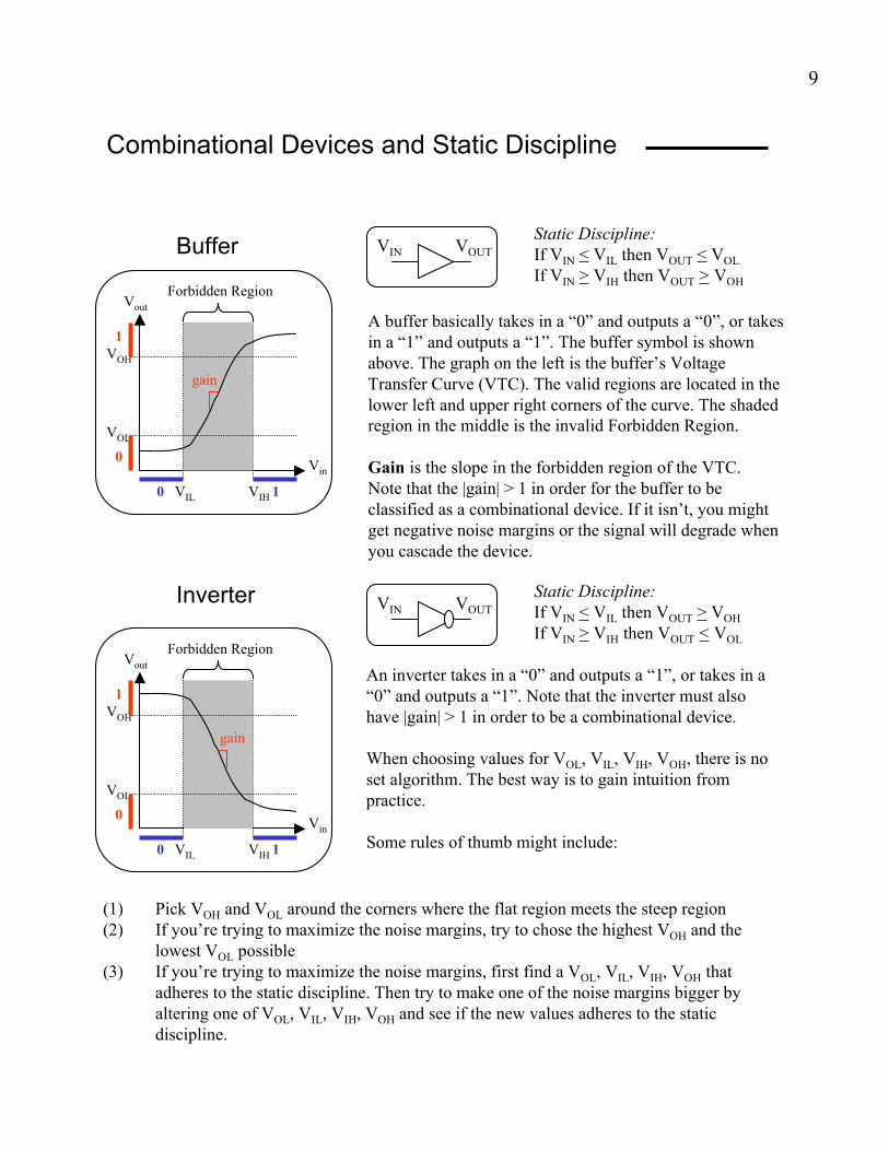
Combinational Devices and Static Discipline
A buffer basically takes in a “0” and outputs a “0”, or takes
in a “1” and outputs a “1”. The buffer symbol is shown
above. The graph on the left is the buffer’s Voltage
Transfer Curve (VTC). The valid regions are located in the
lower left and upper right corners of the curve. The shaded
region in the middle is the invalid Forbidden Region.
Gain is the slope in the forbidden region of the VTC.
Note that the |gain| > 1 in order for the buffer to be
classified as a combinational device. If it isn’t, you might
get negative noise margins or the signal will degrade when
you cascade the device.
VIN VOUT
VIN VOUT
Static Discipline:
If VIN < VIL then VOUT < VOL
If VIN > VIH then VOUT > VOH
Static Discipline:
If VIN < VIL then VOUT > VOH
If VIN > VIH then VOUT < VOL
An inverter takes in a “0” and outputs a “1”, or takes in a
“0” and outputs a “1”. Note that the inverter must also
have |gain| > 1 in order to be a combinational device.
When choosing values for VOL, VIL, VIH, VOH, there is no
set algorithm. The best way is to gain intuition from
practice.
Some rules of thumb might include:
VOL
VOH
VIL VIH
Forbidden RegionVout
Vin
gain
0
0
1
1
VOL
VOH
VIL VIH
Forbidden RegionVout
Vin
gain
0
0 1
1
(1) Pick VOH and VOL around the corners where the flat region meets the steep region
(2) If you’re trying to maximize the noise margins, try to chose the highest VOH and the
lowest VOL possible
(3) If you’re trying to maximize the noise margins, first find a VOL, VIL, VIH, VOH that
adheres to the static discipline. Then try to make one of the noise margins bigger by
altering one of VOL, VIL, VIH, VOH and see if the new values adheres to the static
discipline.
Inverter
Buffer

10
NFET pulldowns
A NFET can be categorized into three “analog” regions –
cutoff, linear, and saturation - and two “digital”regions – on
and off.
Off/Cutoff: VGS < VTH
On/Linear: VGS > VTH, VDS < VDSsat
On/Saturation: VGS > VTH, VDS > VDSsat
Where VDSsat = VGS – VTH
VTH = a set Threshold Voltage
G
D
S
VDS
VGS
PFET pullups
A PFET also has three “analog” regions – cutoff, linear, and
saturation - and two “digital”regions – on and off.
Off/Cutoff: VGS > VTH
On/Linear: VGS < VTH, VDS > VDSsat
On/Saturation: VGS < VTH, VDS < VDSsat
Where VDSsat = VGS - VTH
G
D
S
VDS
VGS
CMOS Inverter
VIN VOUTIN OUT
0 1
1 0
VIL VIH
VOL
VOH
IN OUT
IN = 0
PFET ON
NFET OFF
OUT = 1
IN = 1
PFET OFF
NFET ON
OUT = 0
A CMOS inverter has one PFET between power and
the output, and one NFET between the output and
ground. Think of the PFET and NFET as switches.
A PFET “switch” closes when IN=0, and ties the
output to VDD. A NFET “switch” closes when IN=1,
and ties the output to ground.

11
CMOS Logic
A CMOS Logic gate consists of a bunch of PFETs in the pullup
(between power and the output), and a bunch of NFETs in the pulldown
(between the output and ground).
The pullup may only consist of PFETs and the pulldown may
only consist of NFETs. Otherwise, the logic gate will not have
sufficient gain in the forbidden area. Also, since the NFETs always go in
the pulldown, CMOS logic gates can only implement negative logic.
Pullup PFETs
Pulldown NFETs
I
N
P OUTPUT
U
T
S
A
B
A B
The pullup and pulldown must complement each other.A BIf two NFETs are in parallel in the pulldown, then the
corresponding PFETs must be in series in the pullup.A
The opposite is also true – NFETs in series must have
corresponding PFETs in parallel. B
If you have a formula that you need to implement as a CMOS logic gate:
A*B means A and B are in series in the pulldown and in parallel in the pullup
A+B means A and B are in parallel in the pulldown and in series in the pullup
First draw the pulldown. Then after the pulldown is done, draw the pullup as the
complement of the pulldown. In the example below, we must draw the CMOS logic gate
for OUTPUT = A * B + C.
OUT = A*B + C
NFET: A and B in series
A
B
OUT = A*B + C
NFET: A*B in parallel with C
A
BC
OUT = A*B + C
PFET: A and B in parallel
A B
OUT = A*B + C
PFET: A*B in series with C
A B
C
A
BC
A B
C

12
If you have a CMOS logic gate and you wish to derive the formula, follow these steps:
1) Look at the pulldown only
2) A and B in series means there is an “A*B” in the equation
3) A and B in parallel means there is an “A+B” in the equation
4) Negate the entire thing after you’re done with all the pulldown NFETs.
Step 4 is necessary because you’re dealing with NFETs. You will probably want to do a
few similar practice problems to gain intuition.
A
BC
A and B are in series
A*B
A
BC
A*B is in parallel with C
OUTPUT = A*B + C

13
CMOS Logic Gates
INVERTER
A Z
A Z
0 1
1 0
BUFFER
A Z
A Z
0 0
1 1
NAND
A
B
Z
A B Z
0 0 1
0 1 1
1 0 1
1 1 0
AND
A
B
Z
A B Z
0 0 0
0 1 0
1 0 0
1 1 1
NOR
A B Z
0 0 1
0 1 0
1 0 0
1 1 0
A
B
Z
OR
A B Z
0 0 0
0 1 1
1 0 1
1 1 1
A
B
Z
XNOR
A B Z
0 0 1
0 1 0
1 0 0
1 1 1
XOR
A B Z
0 0 0
0 1 1
1 0 1
1 1 0
A
B
Z
A
B
Z
The figures above contain eight typical standard CMOS logic gates, their symbolic
representation, and their truth tables. You can combine logic gates to implement almost any
function. However, keep in mind that negative logic (inverter, nand, nor, xnor) is usually
smaller and faster than positive logic (buffer, and, or, xor).
Boolean Algebra
A * B means “A and B”
A * B means “A nand B”
A + B means “A or B”
A + B means “A nor B”
A + B means “A xor B”
A + B means “A xnor B”
DeMorgan’s Law
A * B = A + B
A + B = A * B

14
If you wish to derive a logic equation
from an existing circuit, try to derive
intermediate equations, starting at the
inputs and working incrementally
towards the output. You can use
boolean algebra to manipulate the
formula to whatever format you prefer.
A
B
A*B
C C
A A Z = A + A*B + C
Z = A * A*B * C
Z = A * A*B * C
Z = A*B*C
A
B C
Z = A*B+CA*B
Z = A*B + C
Z = A*B * C
Invert it twice (two bars)
DeMorganize the bottom bar
A
B
A*B
C C
Z
Buildings Circuits with Logic Gates
If you wish to implement a function Z = A*B + C using only standard logic gates such as
those pictured above, you can implement it in multiple ways. The two possibilities below (all
negative logic on the left and all positive logic on the right) are not necessarily faster or
smaller than one another – it depends on the size and speed of the standard logic gates.
Contamination Delay
The contamination delay of a circuit, tcd, is
the minimum amount of time it takes for an
invalid input to propagate to an invalid
output. The figure to the right illustrates the
measurement of a buffer’s contamination
delay.
For a circuit with multiple inputs or paths to
the output, the contamination delay of the
entire circuit is the sum of the contamination
delays in the shortest path. For example, the
circuit to the right has three paths, with the
shortest contamination delay through the
bottom path for a tcd = (2.5 + 3) = 5.5
X
X
tcd
A
Z
A Z
A
B
C
Z
tcd=1tcd=2
tcd=2.5tcd=3

15
Sum of Products
Sum of Products is an easy way to derive a formula from a
truth table. The formula is a sum of products. Each product
represents one row where the output Z = 1. For each
product/row, write down all the inputs and put individual
bars over the inputs that equal zero.
If there are fewer Z = 0 than Z = 1 outputs, you can find the
sum of products using the same method, but use the Z = 0
rows as the products and negate the entire sum of products.
From here, you should be able to find the minimal sum of
products by reducing the formula using boolean arithmetic.
This can be quite tedious. An easier method for finding the
minimal sum of products is presented in a subsequent
section on Karnaugh Maps.
A B C Z
0 0 0 0
0 0 1 0
0 1 0 1
0 1 1 0
1 0 0 0
1 0 1 1
1 1 0 0
1 1 1 1
A B C
A B C
A B C
Z = ABC + ABC + ABC
Propagation Delay
The propagation delay, tpd, is the maximum
amount of time it takes for a valid input to
propagate to a valid output. The figure to the
right illustrates the measurement of a buffer’s
propagation delay.
For a circuit with multiple inputs or paths to
the output, the propagation delay of the entire
circuit is the sum of the propagation delays in
the longest path. For example, the circuit to
the right has three paths, with the longest
propagation delay through the middle path
for a tpd = (3 + 2 + 5) = 10
X
X
tpd
A
Z
A Z
A
B
C
Z
tpd=1tpd=2
tpd=3tpd=5

16
Karnaugh Maps
Karnaugh Maps are extremely useful for finding the minimal sum of products.
Translate a truth table to a Karnaugh Map.
" Note the order of the AB field – neighbors must differ by one bit1
A B C Z
0 0 0 1
0 0 1 0
0 1 0 X
0 1 1 0
1 0 0 1
1 0 1 X
1 1 0 X
1 1 1 X
C
00 01 11 10
0 1 X X 1
1 0 1 X X
A
AB
C
B
Find and circle all 1’s
- Don’t Cares ‘X’ can be circled, if needed
- Circles must have dimensions that are a power of 2 (1, 2, 4, 8, etc.)
2
- You can overlap circles
- The Karnaugh Map folds over, so circles can go off the sides
- Look for the largest groups of 1’s
- Try to get the smallest number of circles
C
00 01 11 10
0 1 X X 1
1 0 1 X X
A
AB
C
B
OUT = C + B + A3
C
00 01 11 10
00 1 0 0 1
01 0 1 1 0
11 0 1 1 0
10 1 0 0 1
A
AB
CD
B
D
OUT = B D + B D
Lenient Combinational Logic
Take a karnaugh map that is directly derived from the
circuit. Each gap between neighboring circles is an
opportunity for a glitch. The circuit is lenient if there
are no gaps.
00 01 11 10
0 0 1 1 0
1 0 1 1 1
AB
C

17
Mux
A d-input mux has a selector input, d data inputs (d is a power of two), and one output.
D0
D1
0
1
OUTIf Select = 0, then OUT = D0
If Select = 1, then OUT = D1
Select
D0 D1 Select OUT
0 X 0 0
1 X 0 1
X 0 1 0
X 1 1 1
ROM / PLA
A Read-Only Memory and a Programmable
Logic Array consist of address input lines, word
lines, and bit lines. You can add NFETs to
configure the ROM or PLA to perform many
functions. Each word line and bit line is driven
by a weak PFET whose input is tied to ground.
The weak PFET serves to drive the wire high
when there is no path to ground, but is easily
overpowered by a NFET.A B Z
A ROM specifies all combinations of inputs. A PLA looks like a small ROM because
unnecessary FETs and wires are eliminated. If you are given the PLA pictured above, follow
these steps to figure out the formula for the output:
1. Write the logic equivalent of each word line at the top
2. Each bit line driving the gate of a NFET is a product in the sum of products
3. For each NFET drain attached to the bit line, negate the gate input.
Repeat to find product.
4. Z = OR of all the products
A B Z = A B + A B
A A B B
A B
A B
products
Sum of products
Weak PFET
18
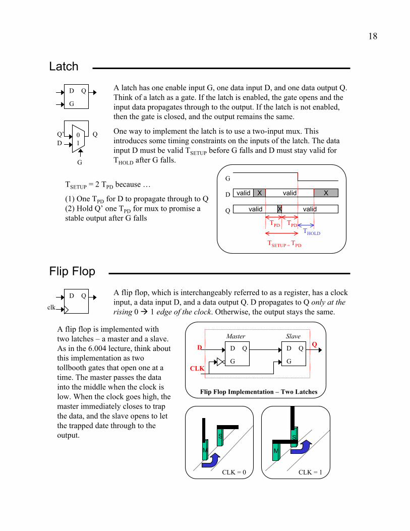
Latch
A latch has one enable input G, one data input D, and one data output Q.
Think of a latch as a gate. If the latch is enabled, the gate opens and the
input data propagates through to the output. If the latch is not enabled,
then the gate is closed, and the output remains the same.
One way to implement the latch is to use a two-input mux. This
introduces some timing constraints on the inputs of the latch. The data
input D must be valid TSETUP before G falls and D must stay valid for
THOLD after G falls.
D Q
G
G
D
Q
valid validX X
valid X valid
TPD TPD
THOLD
TSETUP = TPD
TSETUP = 2 TPD because …
(1) One TPD for D to propagate through to Q
(2) Hold Q’ one TPD for mux to promise a
stable output after G falls
0
1
Q’
D
G
Q
Flip Flop
A flip flop, which is interchangeably referred to as a register, has a clock
input, a data input D, and a data output Q. D propagates to Q only at the
rising 0 " 1 edge of the clock. Otherwise, the output stays the same.
D Q
clk
A flip flop is implemented with
two latches – a master and a slave.
As in the 6.004 lecture, think about
this implementation as two
tollbooth gates that open one at a
time. The master passes the data
into the middle when the clock is
low. When the clock goes high, the
master immediately closes to trap
the data, and the slave opens to let
the trapped date through to the
output.
D Q
G
D Q
G
D
CLK
Q
Master Slave
Flip Flop Implementation – Two Latches
M
S
CLK = 0
M
S
CLK = 1
19
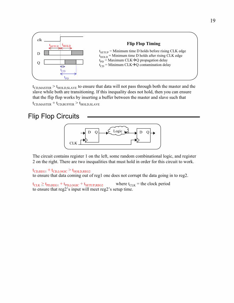
Flip Flop Timing
tSETUP = Minimum time D holds before rising CLK edge
tHOLD = Minimum time D holds after rising CLK edge
tPD = Maximum CLK"Q propagation delay
tCD = Minimum CLK"Q contamination delay
clk
D
Q
tSETUPtHOLD
tCD
tPD
tCD,MASTER > tHOLD,SLAVE to ensure that data will not pass through both the master and the
slave while both are transitioning. If this inequality does not hold, then you can ensure
that the flip flop works by inserting a buffer between the master and slave such that
tCD,MASTER + tCD,BUFFER > tHOLD,SLAVE
Flip Flop Circuits
D Q D QLogic
CLK
The circuit contains register 1 on the left, some random combinational logic, and register
2 on the right. There are two inequalities that must hold in order for this circuit to work.
tCD,REG1 + tCD,LOGIC > tHOLD,REG2
to ensure that data coming out of reg1 one does not corrupt the data going in to reg2.
tCLK > tPD,REG1 + tPD,LOGIC + tSETUP,REG2 where tCLK = the clock period
to ensure that reg2’s input will meet reg2’s setup time.
20
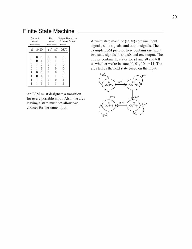
Finite State Machine
A finite state machine (FSM) contains input
signals, state signals, and output signals. The
example FSM pictured here contains one input,
two state signals s1 and s0, and one output. The
circles contain the states for s1 and s0 and tell
us whether we’re in state 00, 01, 10, or 11. The
arcs tell us the next state based on the input.
00
OUT=0
01
OUT=0
11
OUT=1
10
OUT=0
In=0
In=0
In=1
In=1
In=0
In=1
In=0
In=1
An FSM must designate a transition
for every possible input. Also, the arcs
leaving a state must not allow two
choices for the same input.
s1 s0 IN s1’ s0’ OUT
0 0 0 0 0 0
0 0 1 0 1 0
0 1 0 0 1 0
0 1 1 1 0 0
1 0 0 1 0 0
1 0 1 1 1 0
1 1 0 0 0 1
1 1 1 1 1 1
Current Next Output Based on
state state Current State

21
Metastability
A metastable state in the digital world has the following properties:
1) Invalid
2) Unstable – a small perturbation changes it to a 0 or 1
3) It will settle in unbounded time
4) The longer you wait, the more likely it has stabilized
The two-inverter configuration has three possible states where
Vin = Vout : two stable states at valid 1 and 0, and one metastable
state in the forbidden region.
Imagine a ball at the top of a hill. If the hill is not flat, there are three
possible states – a stable state at the bottom left, a stable state at the
bottom right, and a metastable state at the top of the hill. That ball is
in a metastable state because (1) the top of the hill is an unstable state
– a small perturbation will make it roll down the hill, and (2) the ball
will eventually settle to a stable state at the bottom of the hill.
VinVout
Vin=Vout
You cannot build certain devices with perfect reliability because they cause
metastability problems. Some example systems are shown below:
Sample S at a specified time after A and B have risen to find out
which rising edge came first – A or B. The Arbiter may enter a
metastable state if A and B rise at exactly the same time. The
Arbiter will eventually come to decision in unbounded time but
might be metastable and invalid when S is sampled.
Bounded-time ArbiterCANNOT BUILD
ArbiterA
BS
Unbounded-time ArbiterCAN BUILD
ArbiterA
B
S
Done
Sample S when the Done signal is high to find out which
rising edge came first – A or B. S may enter a metastable state
if A and B rise at exactly the same time. However, we are
guaranteed that S will be valid when Done is high, therefore
this arbiter will not cause other metastable states.
If the D input does not meet the flip flop’s setup and hold
time, the Q output might be metastable.
Bounded-time SynchronizerCANNOT BUILD
Asynchronous
SignalD Q
Bounded-time Combinational LogicCAN BUILD
We are guaranteed a valid output after a specified
propagation delay.

22
Unpipelined Circuits
Latency = L = time an input takes to appear at the output
Throughput = T = #outputs / time
The circuit contains multiple blocks of combinational logic,
each with a tCD = 0 and a tPD indicated by the number inside
the box. The latency L of the circuit is the longest path from
the input to the output. The entire circuit is combinational
logic, so the worst-case throughput T is 1 output / L.
1 6
3 3
2
L = 1+6+2 = 9
T = 1 output / 9 = 1/9
Pipelined Circuits
Pipelined circuits contain registers in-between the logic
blocks. For simplicity, we assume that these are ideal
registers with zero contamination and propagation delay,
and zero setup and hold time. The register’s clock cycle tCLK
is equal to the propagation delay of the slowest block.
1 6
3 3
2
L = 6*3 = 18
T = 1/6
Latency = L = K * tPD,slowest stage where K = # stages = # registers on each path
Throughput = T = ____1_______
tPD,slowest stage
Pipelining a circuit typically adds latency and increases throughput. In the example
above, the 6 ns clock cycle forces an input to spend 6 ns in every stage. Since there are
three stages, the input spends 18 ns before its corresponding result appears at the output
as opposed to the unpipelined circuit’s 9 ns latency. However, pipelining the circuit
ensures that a new result appears at the output every 6ns, thus increasing the throughput
to 1/6.
Use the following rules of thumb to pipeline a circuit:
1) Put two dots on opposite sides of the circuit. Draw lines from one
dot to another
2) Always put a register on the output
3) Isolate the slowest block with registers. Make this block the slowest
stage for maximum throughput
4) Never cross a path twice with the same line. This helps ensure that each
path has the same number of registers
5) Add a register every time a line crosses a wire.
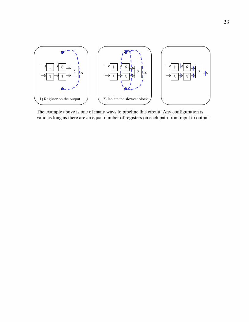
23
1 6
3 3
2
1) Register on the output
1 6
3 3
2
2) Isolate the slowest block
1 6
3 3
2
The example above is one of many ways to pipeline this circuit. Any configuration is
valid as long as there are an equal number of registers on each path from input to output.
24
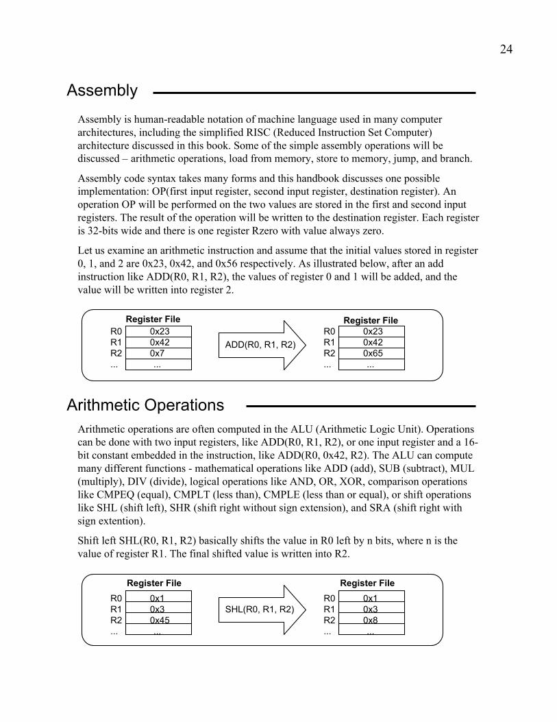
Assembly
Assembly is human-readable notation of machine language used in many computer
architectures, including the simplified RISC (Reduced Instruction Set Computer)
architecture discussed in this book. Some of the simple assembly operations will be
discussed – arithmetic operations, load from memory, store to memory, jump, and branch.
Assembly code syntax takes many forms and this handbook discusses one possible
implementation: OP(first input register, second input register, destination register). An
operation OP will be performed on the two values are stored in the first and second input
registers. The result of the operation will be written to the destination register. Each register
is 32-bits wide and there is one register Rzero with value always zero.
Let us examine an arithmetic instruction and assume that the initial values stored in register
0, 1, and 2 are 0x23, 0x42, and 0x56 respectively. As illustrated below, after an add
instruction like ADD(R0, R1, R2), the values of register 0 and 1 will be added, and the
value will be written into register 2.
R0 0x23
R1 0x42
R2 0x7
... ...
R0 0x23
R1 0x42
R2 0x65
... ...
ADD(R0, R1, R2)
Register File Register File
Arithmetic Operations
Arithmetic operations are often computed in the ALU (Arithmetic Logic Unit). Operations
can be done with two input registers, like ADD(R0, R1, R2), or one input register and a 16-
bit constant embedded in the instruction, like ADD(R0, 0x42, R2). The ALU can compute
many different functions - mathematical operations like ADD (add), SUB (subtract), MUL
(multiply), DIV (divide), logical operations like AND, OR, XOR, comparison operations
like CMPEQ (equal), CMPLT (less than), CMPLE (less than or equal), or shift operations
like SHL (shift left), SHR (shift right without sign extension), and SRA (shift right with
sign extention).
Shift left SHL(R0, R1, R2) basically shifts the value in R0 left by n bits, where n is the
value of register R1. The final shifted value is written into R2.
R0 0x1
R1 0x3
R2 0x45
... ...
R0 0x1
R1 0x3
R2 0x8
... ...
SHL(R0, R1, R2)
Register File Register File

25
There are two types of shift right operations – one without sign extension (SHR), and one
with sign extension (SRA). The sign bit is the most significant bit (MSB), or bit 31 in this
instruction set. When shifting a value to the right, the most significant bits are either
replaced with zero’s if there is no sign extension, or is replaced with the old value of bit 31.
Load
A LOAD instruction loads a value from memory and stores it into a destination register:
LOAD(address register, constant, destination register). The address for memory is
calculated by adding the value in the address register with the constant.
R0 0xF123
R1 0x4
R2 0x7
... ...
R0 0xF123
R1 0x4
R2 0x0F12
... ...
SHR(R0, R1, R2)
R0 0x8123
R1 0x4
R2 0x7
... ...
R0 0x8123
R1 0x4
R2 0xF812
... ...
SRA(R0, R1, R2)
R0 0x7123
R1 0x4
R2 0x7
... ...
R0 0x7123
R1 0x4
R2 0x0712
... ...
SRA(R0, R1, R2)
Register File Register File
R0 0x1
R1 0x3
R2 0x45
... ...
R0 0x1
R1 0x3
R2 0x8
... ...
LD(R0, 0x4, R2)
Addr Value
...
0x4 0x3
0x5 0x8
... ...
Addr Value
...
0x4 0x3
0x5 0x8
... ...
Register File Register File
Data Memory Data Memory

26
Store
A STORE instruction stores a register value to memory. STORE(value register, constant,
address register). The address for memory is calculated by adding the value in the address
register with the constant.
R0 0x1
R1 0x3
R2 0x4
... ...
R0 0x1
R1 0x3
R2 0x4
... ...
ST (R0, 0x1, R2)
Addr Value
...
0x4 0x9
0x5 0x8
... ...
Addr Value
...
0x4 0x9
0x5 0x1
... ...
Data Memory Data Memory
Register File Register File
Branch
A branch instruction is an assembly version of an if-then-else construct. IF the value of the
comparison register meets a certain criteria, THEN the computer will branch to the
instruction indicated by the label, ELSE go to the next instruction in the sequence. If the
operation does indeed branch, then a pointer will be stored in the instruction address
destination register. Branch instructions include BEQ/BF (equal to zero) and BNE/BT (not
equal to zero).
BEQ(comparison register, label, instruction address destination register).
For example, the following is an assembly implementation of “if (a=0) then b=2”
start: LD(Rzero, a, R0) // load value of a into register R0
BEQ(a, btwo, R1) // if a=0, then branch to “btwo” and store instruction pointer in R1
...
btwo: ADDC(Rzero, 0x2, R0) // R0 = 2
ST(R0, b, Rzero) // b = 2
...
27
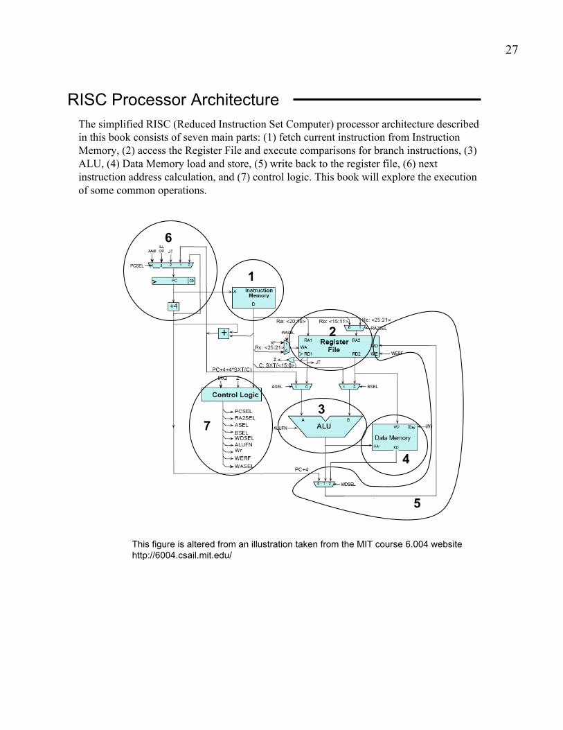
RISC Processor Architecture
The simplified RISC (Reduced Instruction Set Computer) processor architecture described
in this book consists of seven main parts: (1) fetch current instruction from Instruction
Memory, (2) access the Register File and execute comparisons for branch instructions, (3)
ALU, (4) Data Memory load and store, (5) write back to the register file, (6) next
instruction address calculation, and (7) control logic. This book will explore the execution
of some common operations.
This figure is altered from an illustration taken from the MIT course 6.004 website
http://6004.csail.mit.edu/
6
1
2
3
4
5
7
28
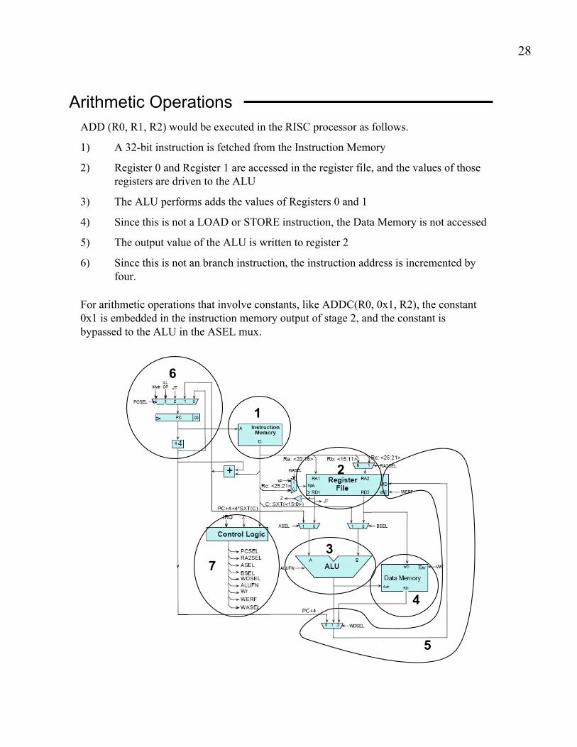
Arithmetic Operations
ADD (R0, R1, R2) would be executed in the RISC processor as follows.
1) A 32-bit instruction is fetched from the Instruction Memory
2) Register 0 and Register 1 are accessed in the register file, and the values of those
registers are driven to the ALU
3) The ALU performs adds the values of Registers 0 and 1
4) Since this is not a LOAD or STORE instruction, the Data Memory is not accessed
5) The output value of the ALU is written to register 2
6) Since this is not an branch instruction, the instruction address is incremented by
four.
For arithmetic operations that involve constants, like ADDC(R0, 0x1, R2), the constant
0x1 is embedded in the instruction memory output of stage 2, and the constant is
bypassed to the ALU in the ASEL mux.
6
1
2
3
4
5
7

29
Load
LD (R0, 0x4, R2) would be executed in the RISC processor as follows.
1) A 32-bit instruction is fetched from the Instruction Memory
2) Register 0 is accessed in the Register File, and the value is driven to the ALU
3) The ALU calculates the Data Memory address by adding the value of Register 0
and the constant 0x4
4) The Data Memory is accessed and the data is output to the wdsel mux
5) The contents of Data Memory are loaded into Register 2
6) Since this is not an branch instruction, the instruction address is incremented by
four.
6
1
2
3
4
5
7
30
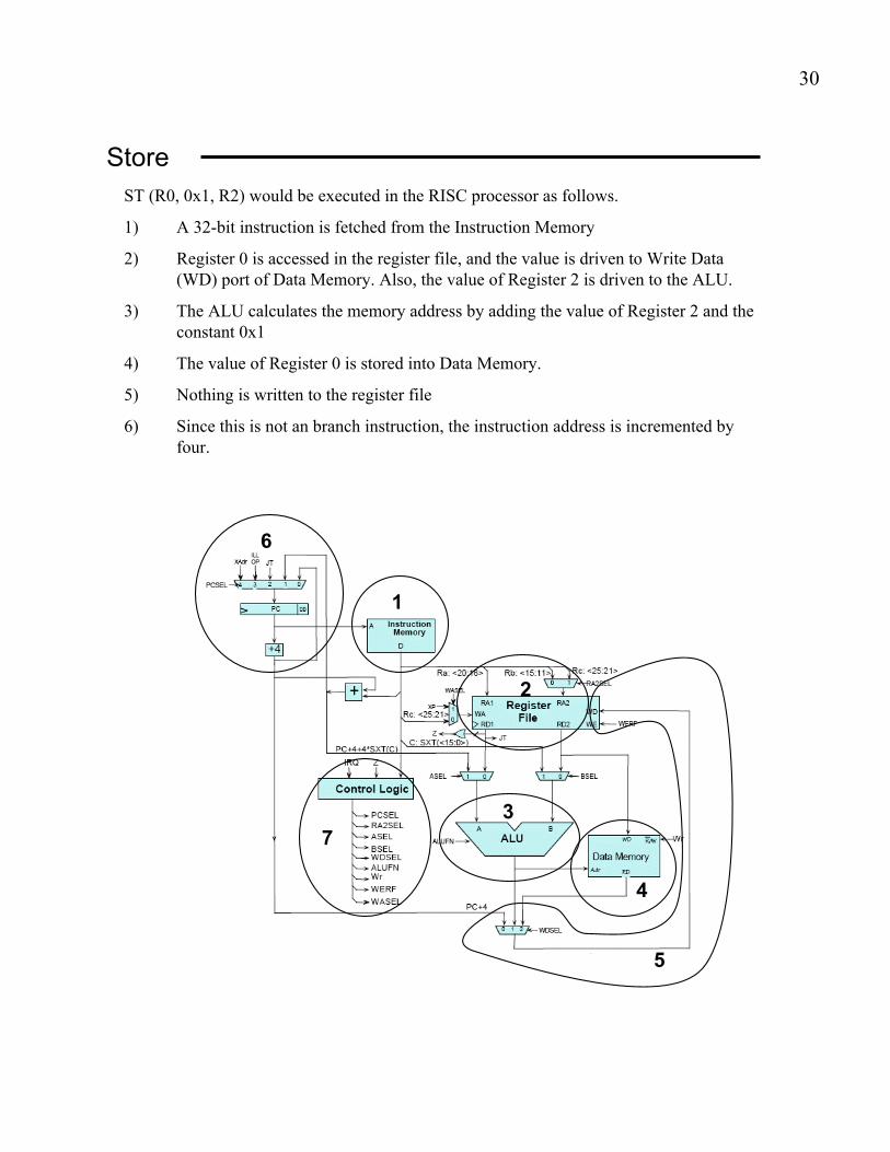
Store
ST (R0, 0x1, R2) would be executed in the RISC processor as follows.
1) A 32-bit instruction is fetched from the Instruction Memory
2) Register 0 is accessed in the register file, and the value is driven to Write Data
(WD) port of Data Memory. Also, the value of Register 2 is driven to the ALU.
3) The ALU calculates the memory address by adding the value of Register 2 and the
constant 0x1
4) The value of Register 0 is stored into Data Memory.
5) Nothing is written to the register file
6) Since this is not an branch instruction, the instruction address is incremented by
four.
6
1
2
3
4
5
7
31
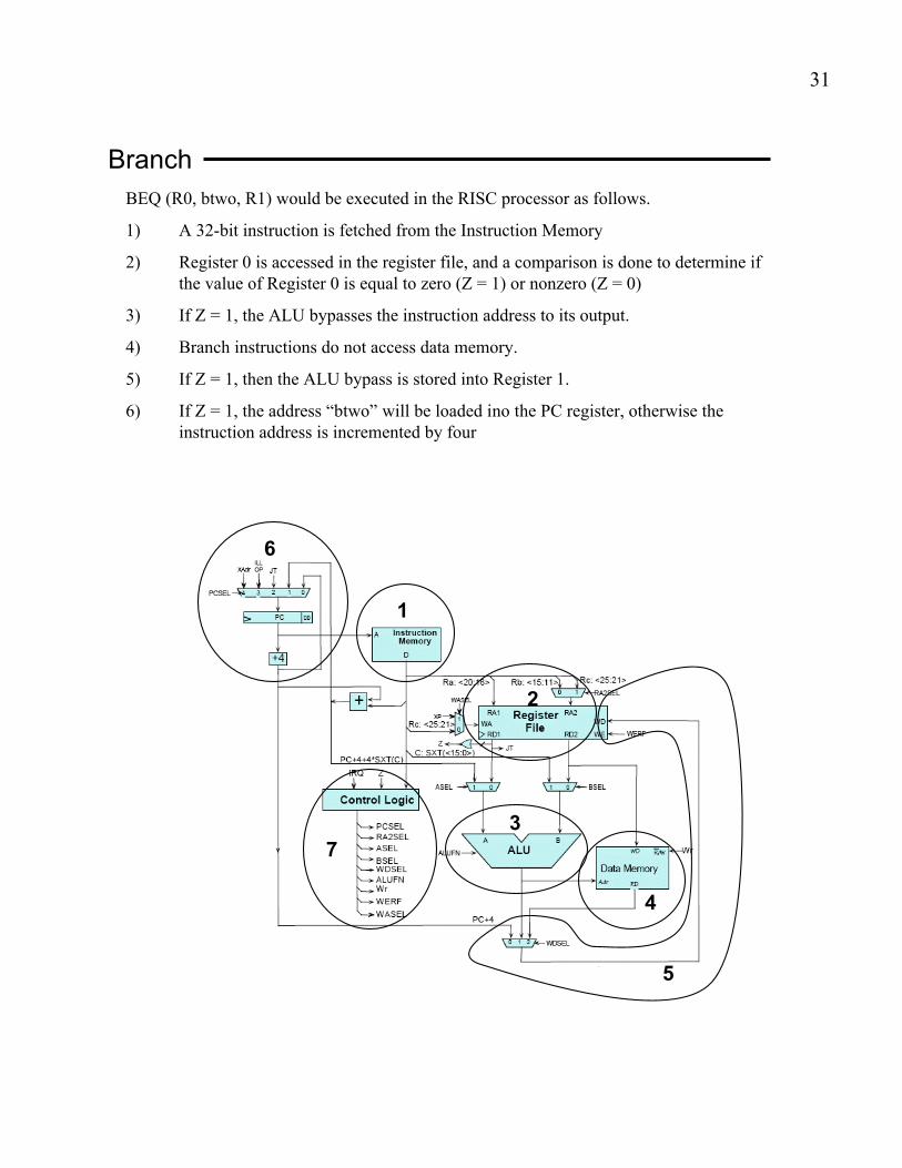
Branch
BEQ (R0, btwo, R1) would be executed in the RISC processor as follows.
1) A 32-bit instruction is fetched from the Instruction Memory
2) Register 0 is accessed in the register file, and a comparison is done to determine if
the value of Register 0 is equal to zero (Z = 1) or nonzero (Z = 0)
3) If Z = 1, the ALU bypasses the instruction address to its output.
4) Branch instructions do not access data memory.
5) If Z = 1, then the ALU bypass is stored into Register 1.
6) If Z = 1, the address “btwo” will be loaded ino the PC register, otherwise the
instruction address is incremented by four
6
1
2
3
4
5
7
32
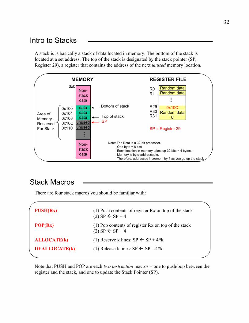
Intro to Stacks
A stack is is basically a stack of data located in memory. The bottom of the stack is
located at a set address. The top of the stack is designated by the stack pointer (SP,
Register 29), a register that contains the address of the next unused memory location.
data
data
data
unused
unused
Bottom of stack
Top of stack
SP
Non-
stack
data
MEMORY
Non-
stack
data
Area of
Memory
Reserved
For Stack
REGISTER FILE
Note: The Beta is a 32-bit processor.
One byte = 8 bits
Each location in memory takes up 32 bits = 4 bytes.
Memory is byte-addressable.
Therefore, addresses increment by 4 as you go up the stack
Random data
Random data
0x10C
Random data
0
R0
R1
R29
R30R31
0x100
0x104
0x108
0x10C
0x110
0x0
SP = Register 29
Stack Macros
There are four stack macros you should be familiar with:
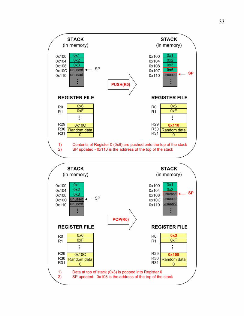
PUSH(Rx) (1) Push contents of register Rx on top of the stack
(2) SP ! SP + 4
POP(Rx) (1) Pop contents of register Rx on top of the stack
(2) SP ! SP + 4
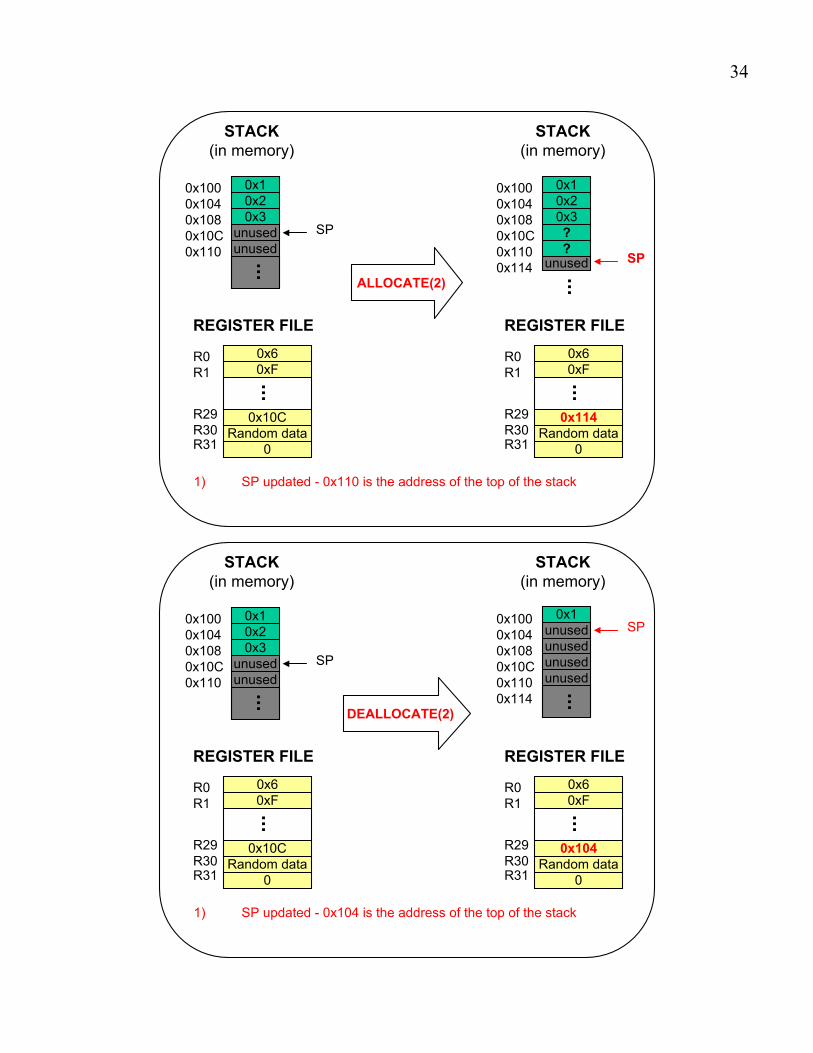
ALLOCATE(k) (1) Reserve k lines: SP ! SP + 4*k
DEALLOCATE(k) (1) Release k lines: SP ! SP – 4*k
Note that PUSH and POP are each two instruction macros – one to push/pop between the
register and the stack, and one to update the Stack Pointer (SP).
33
0x1
0x2
0x3
unused
unused
SP
STACK(in memory)
REGISTER FILE
0x6
0xF
0x10C
Random data
0
R0
R1
R29
R30R31
0x100
0x104
0x108
0x10C
0x110
PUSH(R0)
0x1
0x2
0x3
unused SP
STACK(in memory)
REGISTER FILE
0x6
0xF
0x110Random data
0
R0
R1
R29
R30R31
0x100
0x104
0x108
0x10C
0x110
0x6
0x1
0x2
0x3
unused
unused
SP
STACK(in memory)
REGISTER FILE
0x6
0xF
0x10C
Random data
0
R0
R1
R29
R30R31
0x100
0x104
0x108
0x10C
0x110
0x1
0x2
unused
SP
STACK(in memory)
REGISTER FILE
0x30xF
0x108Random data
0
R0
R1
R29
R30R31
0x100
0x104
0x108
0x10C
0x110
unused
unused
POP(R0)
1) Contents of Register 0 (0x6) are pushed onto the top of the stack
2) SP updated - 0x110 is the address of the top of the stack
1) Data at top of stack (0x3) is popped into Register 0
2) SP updated - 0x108 is the address of the top of the stack
34
0x1
0x2
0x3
unused
unused
SP
STACK(in memory)
REGISTER FILE
0x6
0xF
0x10C
Random data
0
R0
R1
R29
R30R31
0x100
0x104
0x108
0x10C
0x110
ALLOCATE(2)
0x1
0x2
0x3
unused SP
STACK(in memory)
REGISTER FILE
0x6
0xF
0x114Random data
0
R0
R1
R29
R30R31
0x100
0x104
0x108
0x10C
0x110
0x114
?
1) SP updated - 0x110 is the address of the top of the stack
?
0x1
0x2
0x3
unused
unused
SP
STACK(in memory)
REGISTER FILE
0x6
0xF
0x10C
Random data
0
R0
R1
R29
R30R31
0x100
0x104
0x108
0x10C
0x110
DEALLOCATE(2)
0x1
STACK(in memory)
REGISTER FILE
0x6
0xF
0x104Random data
0
R0
R1
R29
R30R31
0x100
0x104
0x108
0x10C
0x110
0x114
1) SP updated - 0x104 is the address of the top of the stack
unused
unused
SPunused
unused

35
Stack Frames
Stack frames allow procedures to call other
procedures (caller calls the callee), and prevent
procedures from corrupting each other’s data.
Two new registers are added to support Stack
Frames. Register 27, Base Pointer BP, points to
local variable 0 in the frame and is used to access
the procedure’s arguments and local variables.
Register 28, Link Pointer LP, contains the return
address of the caller. As stated in previous
sections, Register 29 is the Stack Pointer SP.
A stack frame consists of (1) arguments pushed
in reverse order, (2) the caller’s link pointer, (3)
the caller’s base pointer, and (4) a bunch of local
variables.
arg n
…
arg 0
old LP
old BP
local var. 0
…
local var. n
unused
A portion of the STACK(in memory)
arg n
…
arg 0
old old LP
old old BP
local var. 0
…
local var. n
…
…
Callee’s
Frame
Caller’s
Frame
SP
BP
old BP
Two-level stack example
In this example, we have a caller main and a callee f. The initial state of the stack is
pictured below. Main has been running for awhile and is about to call f. The program code
arrow points to the line that is about to be executed. To conserve space, only relevant
portions of the program code are shown in each snapshot.
unused
Main’s args
Main’s LP
Main’s caller’s BP
local var. 0
local var. 1
…
…
SP
BP
Stack(in memory)
Register File
?
?
0x114
?
0
R0
R1
BP
LP
SP
R30
R31
0x100
0x104
0x108
0x10C
0x110
0x114
….
0x004
0x10C
Main: ….
….
PUSH(b)
PUSH(a)
BR(f, LP)
….
f: ….
0xC00
0xC04
0xC08
0xC0C
Program code(in memory)
(1) Initial State: Main is about to call helper procedure f
The code shown in Main is a typical calling sequence.

36
unused
Main’s args
Main’s LP
Main’s caller’s BP
local var. 0
local var. 1
…
…
SP
BP
Stack(in memory)
Register File
?
?
0x11C?
0
R0
R1
BP
LP
SP
R30
R31
0x100
0x104
0x108
0x10C
0x110
0x114
0x118
0x11C
…
0x004
0x10C
Main: ….
….
PUSH(b)
PUSH(a)
BR(f, LP)
….
f: ….
0xC00
0xC04
0xC08
0xC0C
Program code(in memory)
(2) Main pushed f’s arguments onto the stack in reverse order
b
a
unused
Main’s args
Main’s LP
Main’s caller’s BP
local var. 0
local var. 1
…
…
SP
BP
Stack(in memory)
Register File
?
?
0x11C
?
0
R0
R1
BP
LP
SP
R30
R31
0x100
0x104
0x108
0x10C
0x110
0x114
0x118
0x11C
…
0xC0C0x10C
Main: ….
….
PUSH(b)
PUSH(a)
BR(f, LP)
….
f: ….
0xC00
0xC04
0xC08
0xC0C
Program code(in memory)
(3) Main branched to f and stores return address in LP
b
a
unused
Main’s args
Main’s LP
Main’s caller’s BP
local var. 0
local var. 1
…
…SP
BP
Stack(in memory)
Register File
?
?
0x124?
0
R0
R1
BP
LP
SP
R30
R31
0x100
0x104
0x108
0x10C
0x110
0x114
0x118
0x11C
0x120
0x124
…
0xC0C
0x10C
Main: ….
f: ….
PUSH(LP)
PUSH(BP)
MOVE(SP,BP)
ALLOCATE(2)
Program code(in memory)
(4) f pushed the return address (LP) and Main’s BP
The code shown in f is a typical entry sequence.
b
a
0xC00
0xC04
0xC08
0xC0C
0xC0C0x10C

37
unused
Main’s args
Main’s LP
Main’s caller’s BP
local var. 0
local var. 1
…
…SP
BP
Stack(in memory)
Register File
?
?
0x124
?
0
R0
R1
BP
LP
SP
R30
R31
0x100
0x104
0x108
0x10C
0x110
0x114
0x118
0x11C
0x120
0x124
…
0xC0C
0x124
Main: ….
f: ….
PUSH(LP)
PUSH(BP)
MOVE(SP,BP)
ALLOCATE(2)
Program code(in memory)
(5) f updated BP to reflect the current stack frame
b
a
0xC00
0xC04
0xC08
0xC0C
0xC0C
0x10C
Main’s args
Main’s LP
Main’s caller’s BP
local var. 0
local var. 1
…
… SP
BP
Stack(in memory)
Register File
?
?
0x12C?
0
R0
R1
BP
LP
SP
R30
R31
0x100
0x104
0x108
0x10C
0x110
0x114
0x118
0x11C
0x120
0x124
0x128
0x12C
0xC0C
0x124
Main: ….
f: ….
PUSH(LP)
PUSH(BP)
MOVE(SP,BP)
ALLOCATE(2)
…
Program code(in memory)
(6) f allocated space for two local variables
b
a
0xC00
0xC04
0xC08
0xC0C
0xC100xC0C
0x10C
reserved
reserved

38
Main’s args
Main’s LP
Main’s caller’s BP
local var. 0
local var. 1
…
… SP
BP
Stack(in memory)
Register File
Z?
0x12C
?
0
R0
R1
BP
LP
SP
R30
R31
0x100
0x104
0x108
0x10C
0x110
0x114
0x118
0x11C
0x120
0x124
0x128
0x12C
?
0x124
Main: ….
f: ….
MOVE(val, R0)
MOVE(BP, SP)
POP(BP)
POP(LP)
JMP(LP)
Program code(in memory)
(7) f did some computing and put the return value Z in R0
b
a
0xC30
0xC34
0xC38
0xC3C
0xC400xC0C
0x10C
Local var 0
f loaded argument a into a register using: LD(BP, -12, Reg)
f loaded argument b into a register using: LD(BP, -16, Reg)
f loaded local variable 0 into a register using: LD(BP, 0, Reg)
f loaded local variable 1 into a register using: LD(BP, 4, Reg)
Local var 1
Main’s args
Main’s LP
Main’s caller’s BP
local var. 0
local var. 1
…
… SP
BP
Stack(in memory)
Register File
Z?
0x12C
?
0
R0
R1
BP
LP
SP
R30
R31
0x100
0x104
0x108
0x10C
0x110
0x114
0x118
0x11C
0xC0C
0x10C
f: ….
MOVE(val, R0)
MOVE(BP, SP)
POP(BP)
POP(LP)
JMP(LP)
Program code(in memory)
(8) f executed a return sequence shown above:
0xC30 - Stored return value into memory
0xC34 - Deallocated local variables by moving SP to BP
0xC38 - Restored the BP
0xC3C - Restored the LP
0xC40 - Jumps to return address stored in LP
b
a
0xC30
0xC34
0xC38
0xC3C
0xC40
Main: ….
BR(f, LP)
….
0xC08
0xC0C

39
Memory Hierarchy
Memory is one of the bottlenecks of a pipelined processor. We can alleviate this
bottleneck with a hierarchy – a small fast cache (often notated as “$”), a larger slower
main memory, and an enormous but very slow disk. Main memory has everything the
cache has and more. Similarly, disk has everything contained in main memory and more.
When the CPU accesses a memory location A, it goes through these steps:
(1) Check Cache – If A is in the cache (cache hit), then return DATAA, else go to step 2
(2) Check Main Memory – If A is in memory, then return DATAA and put it in the cache,
else go to step 3.
(3) A will always be in disk. Put A in main memory and the cache, and return the value.
For simplicity, we will assume (for now) that we never have to go to disk – if there is a
cache miss on A, we will always find A in main memory.
Caches are small, fast memory that contain temporary copies of selected memory
locations. For 6.004, you can assume that the CPU runs at a clock speed where a cache hit
on a memory access will return the cache data in one cycle, and a cache miss will cause
the CPU to stall until the data is ready from memory. If the miss rate isn’t too high, using
a cache typically improve the average memory access time.
CPU(Beta) DISK
MainMemory
$
Locality
Caches are useful because they exploit locality in memory accesses. If you access memory
location A, you’re more likely to access A again in the near future. Every time there is a
cache miss, that memory location will go in the cache and replace something that hasn’t
been used for awhile.
tave = tcache + (miss rate) * tmemory
tcache = time it takes to access the cache
tmemory = time it takes to access main memory

40
Fully Associative Cache
A cache contains many cache lines. A cache line contains (1) a valid bit indicating if the
data in that line is valid, (2) optional status bits that indicate if the data is dirty, read-only,
etc., (3) a tag formed from the memory address, and (4) the data corresponding to that
address.
A fully-associative cache is one of the three cache architectures described in this
handbook. It differs from other cache architectures in that it can put data anywhere.
When a memory address is presented to a fully associative cache, the address tag is
compared to tags from all the valid lines in the cache. If there is a match, it’s a cache hit
and the data from that line is sent to the CPU. Otherwise it’s a cache miss.
If there is a cache miss when the cache is full (all the lines are valid), we figure out which
line to replace using one of the replacement policies outlined in a later section. If the line
that is replaced contains valid and dirty data (V=1 and D=1), then we also have to write
the data back to main memory. If it’s not dirty, we just throw the line out.
Some useful equations regarding fully associative caches:
Capacity = # lines * (1 valid bit + S status bits + T tag bits + D data
bits)
Typical values for the 6.004 BETA: T = 30 bits, D = 32 bits
S Tag Data
=?
S Tag Data
=?
S Tag Data
=?
…
TAG 00
Memory Address
from CPU
HIT?
Data from Cache
V
V
V
41
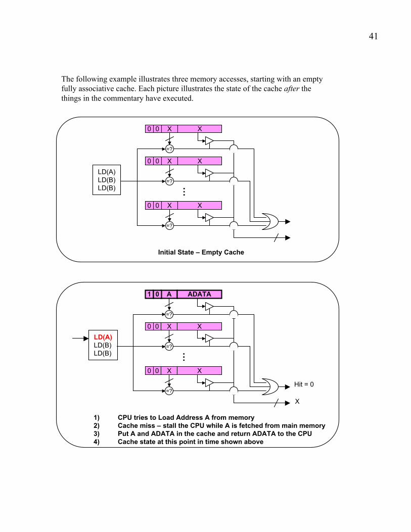
The following example illustrates three memory accesses, starting with an empty
fully associative cache. Each picture illustrates the state of the cache after the
things in the commentary have executed.
0 X X
=?
0 X X
=?
0 X X
=?
…LD(A)
LD(B)
LD(B)
Initial State – Empty Cache
0
0
0
1 A ADATA
=?
0 X X
=?
0 X X
=?
…
LD(A)LD(B)
LD(B)
1) CPU tries to Load Address A from memory2) Cache miss – stall the CPU while A is fetched from main memory3) Put A and ADATA in the cache and return ADATA to the CPU4) Cache state at this point in time shown above
Hit = 0
X
0
0
0

42
1 A ADATA
=?
1 B BDATA
=?
0 X X
=?
…LD(A)
LD(B)LD(B)
1) CPU tries to Load Address B from memory2) Cache miss – stall the CPU while we get B from main memory3) Put B and BDATA in the cache and return BDATA to the CPU
Hit = 0
= X
0
0
0
0 A ADATA
=?
0 B BDATA
=?
0 X X
=?
…
LD(A)
LD(B)
LD(B)
1) CPU tries to Load Address B from memory2) Cache hit – return BDATA to the CPU
Hit = 1
BDATA
0
1
1
43
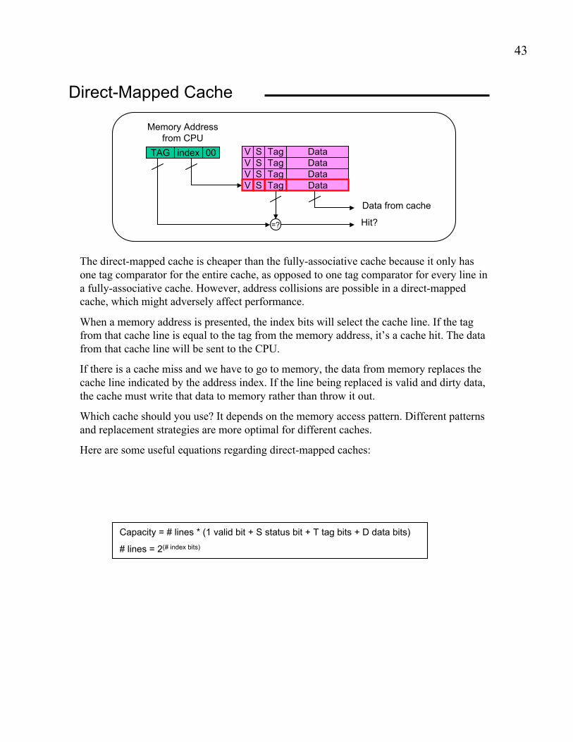
Direct-Mapped Cache
The direct-mapped cache is cheaper than the fully-associative cache because it only has
one tag comparator for the entire cache, as opposed to one tag comparator for every line in
a fully-associative cache. However, address collisions are possible in a direct-mapped
cache, which might adversely affect performance.
When a memory address is presented, the index bits will select the cache line. If the tag
from that cache line is equal to the tag from the memory address, it’s a cache hit. The data
from that cache line will be sent to the CPU.
If there is a cache miss and we have to go to memory, the data from memory replaces the
cache line indicated by the address index. If the line being replaced is valid and dirty data,
the cache must write that data to memory rather than throw it out.
Which cache should you use? It depends on the memory access pattern. Different patterns
and replacement strategies are more optimal for different caches.
Here are some useful equations regarding direct-mapped caches:
Capacity = # lines * (1 valid bit + S status bit + T tag bits + D data bits)
# lines = 2(# index bits)
TAG 00
Memory Address
from CPU
index
=?
Data from cache
Hit?
V Tag DataS
V Tag DataS
V Tag DataS
V Tag DataS

44
=?
Data from cache
Hit?
0 X X0
Initial State – Empty direct-mapped cache
00
01
10
11
0 X X0
0 X X0
0 X X0
The following example illustrates four memory accesses, starting with an empty
direct mapped cache. Each picture illustrates the state of the cache after the
commentary is executed.
001 0001
=?
1 001 DATA00101000
0 X X0
0 X X0
0 X X0
1) LD(0010100) " tagaddress = 001, index = 012) Cache line 01 is not valid, therefore this is a cache miss3) Stall the CPU to find data in main memory4) Store DATA0010100 in cache line 01
00
01
10
11
001 0010
=?
1 001 DATA 00101000
0 X X0
1 001 DATA 00110000
0 X X0
1) LD(0011000) " tagaddress = 001, index = 102) Cache line 10 is not valid, therefore this is a cache miss3) Stall the CPU to find data in main memory4) Store DATA0011000 in cache line 00
00
01
10
11

45
010 0010
=?
1 001 DATA 00101000
0 X X0
1 010 DATA 01010000
0 X X0
1) LD(0101000) " tagaddress = 010, index = 102) Cache line 10 is valid3) Address tag and cache line tag do not match " miss!4) Stall the CPU to find data in memory5) Dirty bit is zero, no need to write DATA0011000 to memory6) Store DATA0101000 in cache line 10
00
01
10
11

46
N-way Set-Associative Cache
A N-way set associative cache is made up of N ways (N direct-mapped caches). Data can
be stored in any one of those ways.
The set-associative cache is a tradeoff between a fully-associative and a direct-mapped
cache. A set-associative cache does not have a lot of expensive tags like a fully-
associative cache. A set-associative cache also cuts down on address collisions by
allowing data to be stored in N cache lines rather than one cache line provided by a direct-
mapped cache.
When a memory address is presented to the set-associative cache, the index bits select a
cache line in all the ways. If the address tag matches any of the tags in the selected cache
lines, it’s a cache hit. The data from that cache line will be sent to the CPU.
If there is a cache miss and we have to go to memory, the data from memory replaces a
cache line in one of the direct-mapped caches. If all the selected cache lines are valid, the
cache uses a replacement policy to determine which should be replaced. Also, if the line
being replaced has valid and dirty data, the cache must write that data to memory.
A set-associative cache has its advantages. However, that does not mean that the set-
associative cache will always perform better than fully-associative or direct-mapped
caches of the same capacity. As stated before, different patterns and replacement
strategies are more optimal for different caches.
Here are some useful equations regarding set-associative caches:
Capacity = (# ways) * (# lines/way) * (1 valid bit + S status bits + T tag bits + D data bits)
# lines = 2(# index bits)
TAG 00
Memory Address
from CPU
index
=?
Data from cache
Hit?
V Tag DataS
V Tag DataS
V Tag DataS
V Tag DataS
…
=?
V Tag DataS
V Tag DataS
V Tag DataS
V Tag DataS
TAGADDR TAGADDR

47
=?
Data from cache
Hit?
0 X X0
0 X X0
0 X X0
0 X X0
=?
Initial State – Empty 2-way Set Associative Cache
0 X X0
0 X X0
0 X X0
0 X X0
The following example illustrates three memory accesses, starting with an empty
2-way set-associative cache. Each picture illustrates the state of the cache after the
things in the commentary have executed.
001 0001
=?
0 X X0
1 001 D00101000
0 X X0
0 X X0
=?
0 X X0
0 X X0
0 X X0
0 X X0
1) LD(0010100) " tagaddress = 001, index = 012) Cache line 01 is invalid in both ways. Cache miss3) Stall the CPU to find data in main memory4) Store D0010100 in cache line 01 in a way
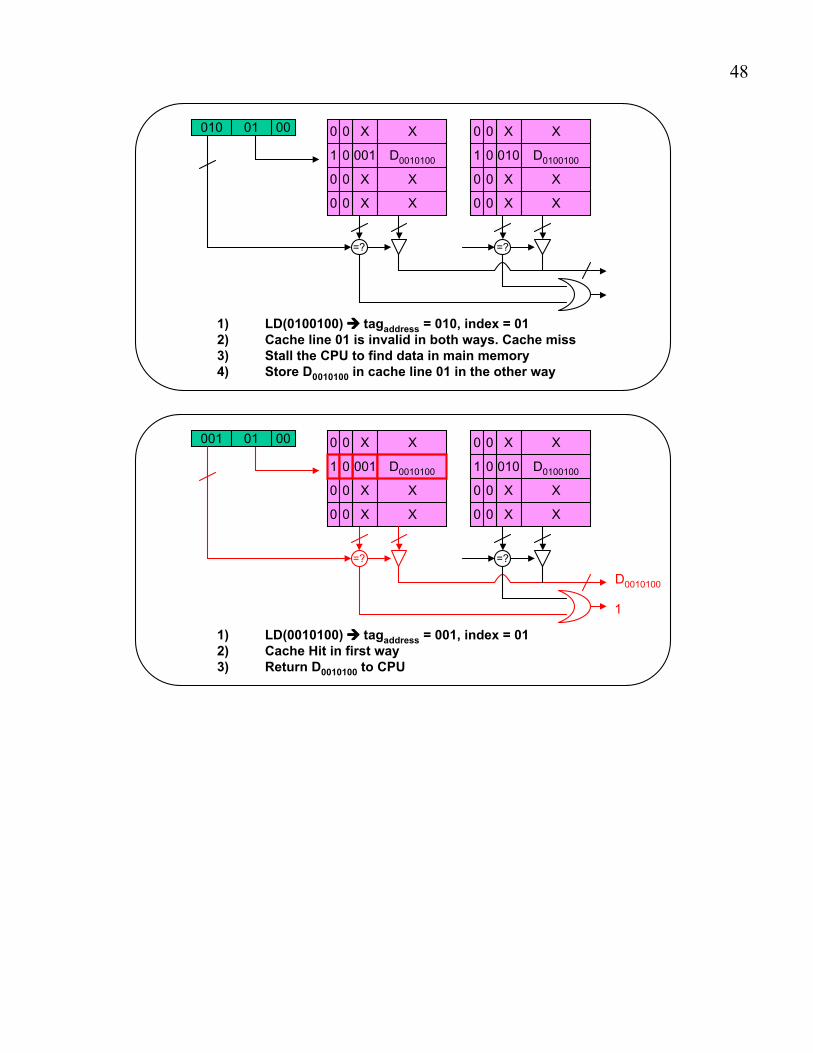
48
010 0001
=?
0 X X0
1 001 D00101000
0 X X0
0 X X0
=?
0 X X0
1 010 D01001000
0 X X0
0 X X0
1) LD(0100100) " tagaddress = 010, index = 012) Cache line 01 is invalid in both ways. Cache miss3) Stall the CPU to find data in main memory4) Store D0010100 in cache line 01 in the other way
001 0001
=?
0 X X0
0 X X0
0 X X0
=?
0 X X0
1 010 D01001000
0 X X0
0 X X0
1) LD(0010100) " tagaddress = 001, index = 012) Cache Hit in first way3) Return D0010100 to CPU
1 001 D00101000
1
D0010100

49
Locality and Data Block Size
If you access memory location A then you’re more likely to access locations near A in the
future. This applies to both data and instruction memory accesses.
Example involving instruction accesses:
CPU instructions are usually executed sequentially through memory (with the exceptions of
jumps and branches). If you fetch an instruction from memory location A, you will likely
need to fetch instructions from A+4, A+8, A+12, etc. in the near future.
Caches can take advantage of locality by increasing the data block size. Whenever there is
a cache miss on memory location A, the cache will put a block of memory surrounding and
including A into the cache.
There are some tradeoffs when it comes to block sizes (assuming a fixed cache capacity).
Advantages of a larger block size
Miss rate decreases if the program
exhibits locality
Disadvantages of a larger block size
More address collisions " miss rate increases
Miss penalty increases (more data is moved
from memory to the cache)
Unnecessary words fetched
Capacity = # lines * (1 valid bit + S status bits + T tag bits + (D data bits/word) * (2b words/line)
S Tag D0
=?…
TAG 00
Memory Address
from CPU
HIT?
Data from Cache
VBlock size D1 … D2b-1
S Tag D0
=?
V D1 … D2b-1
b (to muxes)
b
b
Fully Associative Cache with a data block
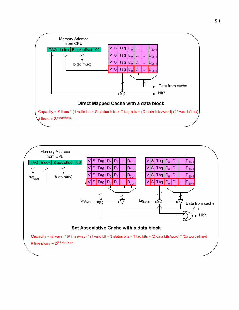
50
Capacity = # lines * (1 valid bit + S status bits + T tag bits + (D data bits/word) (2b words/line)
# lines = 2(# index bits)
TAG 00
Memory Address
from CPU
index
=?
Data from cache
Hit?
Block offset
b (to mux)
S Tag D0V D1 … D2b-1
S Tag D0V D1 … D2b-1
S Tag D0V D1 … D2b-1
S Tag D0V D1 … D2b-1
Direct Mapped Cache with a data block
Capacity = (# ways) * (# lines/way) * (1 valid bit + S status bits + T tag bits + (D data bits/word) * (2b words/line))
# lines/way = 2(# index bits)
TAG 00
Memory Address
from CPU
index
=?
Block offset
b (to mux)
S Tag D0V D1 … D2b-1
S Tag D0V D1 … D2b-1
S Tag D0V D1 … D2b-1
S Tag D0V D1 … D2b-1
…S Tag D0V D1 … D2b-1
S Tag D0V D1 … D2b-1
S Tag D0V D1 … D2b-1
S Tag D0V D1 … D2b-1
=?
tagaddr
tagaddr tagaddr
Hit?
Data from cache
Set Associative Cache with a data block

51
Replacement Policies
Fully-associative and set-associative caches need a replacement policy to decide which
cache line to replace when all options are valid. Three common replacement strategies
include LRU (Least recently used), FIFO (first-in, first-out), and Random.
LRU replaces the least recently used location in the cache. LRU makes sense from a
locality point of view – if certain lines have been used more recently, they are more likely
to be used in the future. LRU is rather costly, however, and is susceptible to memory
patterns that cause worst-case cache performance.
FIFO replaces the oldest item in the cache. FIFO is much cheaper and easier to implement
than LRU, but is also susceptible to worst-case scenario memory patterns that cause worst-
case cache performance.
Random will randomly select a line to be replaced. Random generators that produce a
uniform distribution are difficult to build, possibly less susceptible to worst-case scenarios.
Write Policies
When a cache line is replaced or being written, that line needs to be written to memory at
some point. Three common write policies include write through, write behind, and write
back.
Write through – every time the CPU writes to memory, write to both the cache and main
memory. There are no dirty bits in write through. An advantage to write through is that the
contents of main memory will never be stale. A disadvantage is a sacrifice in performance
from stalling the CPU on every write to memory. For example, a lot of programs contain
functions that repeatedly write to the same variable and then return the final result. All we
need is for the final result to be stored in main memory. Storing the intermediate results in
main memory might be unnecessary.
Write behind – every time the CPU writes to memory, write to the cache and the write
buffer. The CPU then proceeds to the next instruction while the write buffer writes to main
memory in the background. There are no dirty bits in write behind. This usually results in
better performance than write-through, but it is still possible for the write buffer to
unnecessarily write things to memory.
Write-back – every time the CPU writes to memory, the cache will set the dirty bit to one.
On a cache miss, if the cache line being replaced has a dirty bit of one, then that line will be
written to memory. Write back performs well because the cache writes to memory only
when it is absolutely necessary. However, write back sacrifices some area from storing a
dirty bit in each cache line.

52
Virtual Memory
Programs that are run on the CPU commonly use virtual addresses rather than physical
addresses when accessing memory. The CPU’s virtual address is translated by the MMU
(memory management unit) into a physical address that accesses the memory hierarchy.
Physical memory and virtual memory are both divided into sections called pages.
Physical pages have physical page numbers (PPN) and virtual pages have virtual page
numbers (VPN).
The virtual address that is inputted to the MMU contains a virtual page number and a
page offset. The MMU translates the virtual page number into the appropriate physical
page number via a lookup table. The MMU does not touch the page offset.
The output of the MMU is a physical address made up of a physical page number and an
offset. The physical page number points to a page in memory, while the offset indicates
which word to access on that page.
CPU MMU
Memory Hierarchy
$ Main Memory Disk
Virtual
Address
Physical
Address
Using virtual memory has numerous advantages over directly addressing physical
memory. Some (not all) of these advantages are discussed below.
Virtual memory separates hardware from software, thus allowing software to be written
without being constrained by the size of physical memory. This allows programs to use
a huge a virtual memory space that’s larger than physical memory and split up the jobs
between multiple computers. It also allows machines to have more physical memory
than they have in virtual memory.
Virtual memory allows different programs to be isolated from one another, and allows
the operating system to isolate itself from other software. It also allows programs and
their data to be rearranged in physical memory by the operating system in a way that’s
transparent to the program.
53
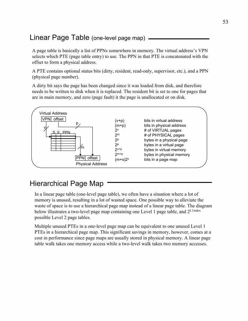
Linear Page Table (one-level page map)
A page table is basically a list of PPNs somewhere in memory. The virtual address’s VPN
selects which PTE (page table entry) to use. The PPN in that PTE is concatenated with the
offset to form a physical address.
A PTE contains optional status bits (dirty, resident, read-only, supervisor, etc.), and a PPN
(physical page number).
A dirty bit says the page has been changed since it was loaded from disk, and therefore
needs to be written to disk when it is replaced. The resident bit is set to one for pages that
are in main memory, and zero (page fault) it the page is unallocated or on disk.
(v+p) bits in virtual address
(m+p) bits in physical address
2v # of VIRTUAL pages
2m # of PHYSICAL pages
2p bytes in a physical page
2p bytes in a virtual page
2v+p bytes in virtual memory
2m+p bytes in physical memory
(m+s)2v bits in a page map
VPN offset
S S PPN
PPN offset
vp
m
Virtual Address
Physical Address
Hierarchical Page Map
In a linear page table (one-level page table), we often have a situation where a lot of
memory is unused, resulting in a lot of wasted space. One possible way to alleviate the
waste of space is to use a hierarchical page map instead of a linear page table. The diagram
below illustrates a two-level page map containing one Level 1 page table, and 2L1index
possible Level 2 page tables.
Multiple unused PTEs in a one-level page map can be equivalent to one unused Level 1
PTEs in a hierarchical page map. This significant savings in memory, however, comes at a
cost in performance since page maps are usually stored in physical memory. A linear page
table walk takes one memory access while a two-level walk takes two memory accesses.
54
D R L2 map
Virtual Address
L1 index offsetL2 index
Level 1
PTBL L1 index
D R PPN
Level 2
L2 map L2 index
Physical Address
PPN offset
(1) PTBL is concatenated with the L1 index to access the Level 1 page map.
R = 0 " Page fault
R = 1 " Page map entry contains a pointer to the Level 2 page map. Go to step
2.
(2) L2map is concatenated with the L2 index to access the level 2 page map.
R = 0 " Page fault
R = 1 " Page map entry contains the PPN. Go to step 3.
(3) Physical address is made of the PPN and the offset from the virtual address.
Translation Look-aside Buffer (TLB)
The TLB is a small, usually fully-associative cache that contains page map entries that
translate VPNs to PPNs. A TLB miss can severely hinder performance because the
page table walk can result in multiple accesses to memory or a page fault.
Caches – Virtual or Physical addresses
Caches that work with physical addresses might not be as advantageous if the we access
main memory during the page table walk. Caches that work with virtual addresses
might perform better, but this brings up issues that are beyond the scope of 6.004. Take
6.823 if you want to learn about these issues.

55
Virtual Address
1
TLB
$VPN PPN
PPNVPN
2
Page Table Walk
3
Page Fault
Software
MMU Overview
The MMU goes through the following steps when it is presented with a virtual address:
1) Check the TLB (Translation Look-aside Buffer). If there is a hit, send the physical
address to memory. If not, go to step 2.
2) Page Table Walk – If the page tables and final physical page reside in memory (not
in disk), then update the TLB and send the physical address to memory. However, if
one of the page tables or the final physical page is not resident in memory, go to step 3.
3) Page Fault – a page table or final physical page resides in disk. Handled in software.
56
References
MIT 6.004 Lecture Notes from Fall 2000 and Spring 2003
MIT 6.823 Lecture Notes from Spring 2003