5v, rail-to-rail i/o, zero-drift, programmable gain ... · • ultra high precision front-end...
TRANSCRIPT
DATASHEET
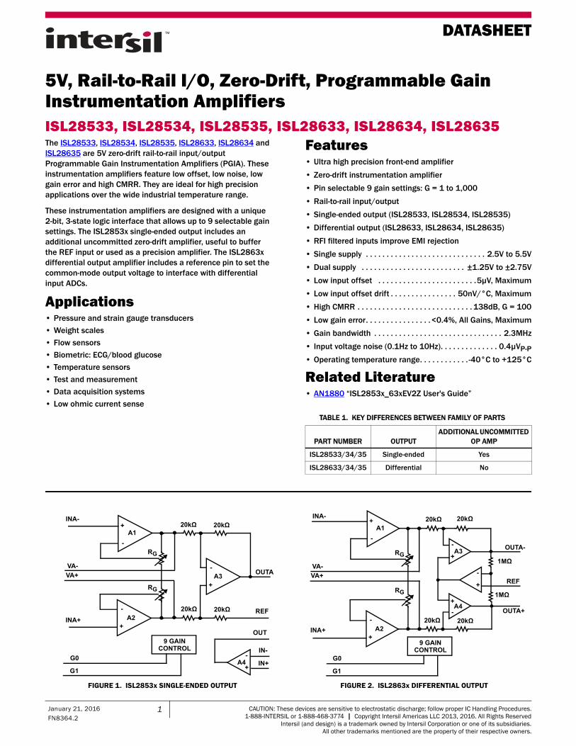
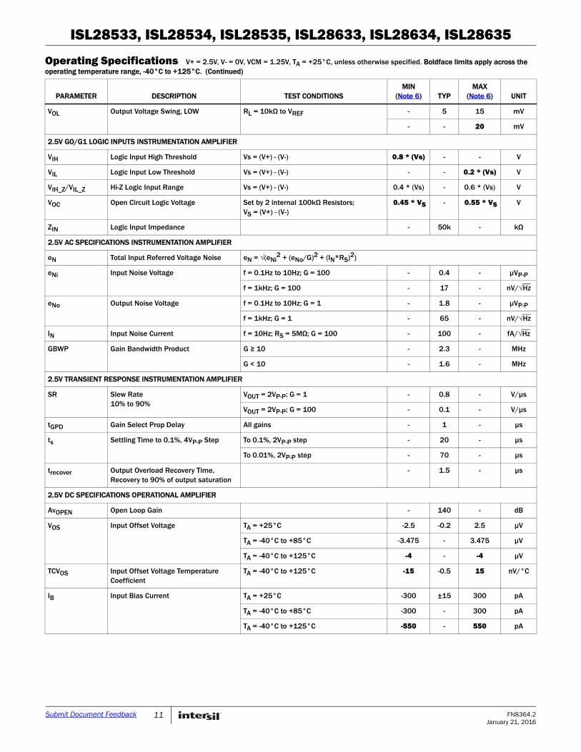
5V, Rail-to-Rail I/O, Zero-Drift, Programmable Gain Instrumentation AmplifiersISL28533, ISL28534, ISL28535, ISL28633, ISL28634, ISL28635The ISL28533, ISL28534, ISL28535, ISL28633, ISL28634 and ISL28635 are 5V zero-drift rail-to-rail input/output Programmable Gain Instrumentation Amplifiers (PGIA). These instrumentation amplifiers feature low offset, low noise, low gain error and high CMRR. They are ideal for high precision applications over the wide industrial temperature range.
These instrumentation amplifiers are designed with a unique 2-bit, 3-state logic interface that allows up to 9 selectable gain settings. The ISL2853x single-ended output includes an additional uncommitted zero-drift amplifier, useful to buffer the REF input or used as a precision amplifier. The ISL2863x differential output amplifier includes a reference pin to set the common-mode output voltage to interface with differential input ADCs.
Applications• Pressure and strain gauge transducers
• Weight scales
• Flow sensors
• Biometric: ECG/blood glucose
• Temperature sensors
• Test and measurement
• Data acquisition systems
• Low ohmic current sense
Features• Ultra high precision front-end amplifier
• Zero-drift instrumentation amplifier
• Pin selectable 9 gain settings: G = 1 to 1,000
• Rail-to-rail input/output
• Single-ended output (ISL28533, ISL28534, ISL28535)
• Differential output (ISL28633, ISL28634, ISL28635)
• RFI filtered inputs improve EMI rejection
• Single supply . . . . . . . . . . . . . . . . . . . . . . . . . . . . . 2.5V to 5.5V
• Dual supply . . . . . . . . . . . . . . . . . . . . . . . . . ±1.25V to ±2.75V
• Low input offset . . . . . . . . . . . . . . . . . . . . . . . .5µV, Maximum
• Low input offset drift . . . . . . . . . . . . . . . . 50nV/°C, Maximum
• High CMRR . . . . . . . . . . . . . . . . . . . . . . . . . . . . 138dB, G = 100
• Low gain error. . . . . . . . . . . . . . . .<0.4%, All Gains, Maximum
• Gain bandwidth . . . . . . . . . . . . . . . . . . . . . . . . . . . . . . . 2.3MHz
• Input voltage noise (0.1Hz to 10Hz). . . . . . . . . . . . . . 0.4µVP-P
• Operating temperature range. . . . . . . . . . . . -40°C to +125°C
Related Literature• AN1880 “ISL2853x_63xEV2Z User's Guide”
TABLE 1. KEY DIFFERENCES BETWEEN FAMILY OF PARTS
PART NUMBER OUTPUTADDITIONAL UNCOMMITTED
OP AMP
ISL28533/34/35 Single-ended Yes
ISL28633/34/35 Differential No
FIGURE 1. ISL2853x SINGLE-ENDED OUTPUT FIGURE 2. ISL2863x DIFFERENTIAL OUTPUT
+
-
+
-
INA-
A2
A1
INA+
+
-
+
-
REF
OUTAA3
A4
RG
RG
9 GAINCONTROL
G0
G1IN+
IN-
OUT
VA-
VA+
20kΩ
20kΩ
20kΩ
20kΩ
+
-
+
-
+
-
INA-
A2
A1
INA+
OUTA-A3RG
RG
G0
G1
+
-
+
- OUTA+
REF
A4
VA-
VA+
20kΩ
20kΩ
20kΩ
20kΩ
9 GAINCONTROL
1MΩ
1MΩ
January 21, 2016 CAUTION: These devices are sensitive to electrostatic discharge; follow proper IC Handling Procedures.
1FN8364.2 1-888-INTERSIL or 1-888-468-3774 | Copyright Intersil Americas LLC 2013, 2016. All Rights ReservedIntersil (and design) is a trademark owned by Intersil Corporation or one of its subsidiaries.All other trademarks mentioned are the property of their respective owners.

ISL28533, ISL28534, ISL28535, ISL28633, ISL28634, ISL28635
Table of ContentsPin Configurations. . . . . . . . . . . . . . . . . . . . . . . . . . . . . . . . . . . . . . . . . . . . . . . . . . . . . . . . . . . . . . . . . . . . . . . . . . . . . . . . . . . . . . . . . . . 3
Pin Descriptions. . . . . . . . . . . . . . . . . . . . . . . . . . . . . . . . . . . . . . . . . . . . . . . . . . . . . . . . . . . . . . . . . . . . . . . . . . . . . . . . . . . . . . . . . . . . . 3
Typical Sensor Application Block Diagram, ISL28533 Single-Ended Output . . . . . . . . . . . . . . . . . . . . . . . . . . . . . . . . . . . . . . . . . . 4
Typical Bridge Sensor Application Block Diagram, ISL28634 Differential Output . . . . . . . . . . . . . . . . . . . . . . . . . . . . . . . . . . . . . 4
G0 and G1 Programmable Gain Setting . . . . . . . . . . . . . . . . . . . . . . . . . . . . . . . . . . . . . . . . . . . . . . . . . . . . . . . . . . . . . . . . . . . . . . . . . 5
Ordering Information . . . . . . . . . . . . . . . . . . . . . . . . . . . . . . . . . . . . . . . . . . . . . . . . . . . . . . . . . . . . . . . . . . . . . . . . . . . . . . . . . . . . . . . . 5
Absolute Maximum Ratings . . . . . . . . . . . . . . . . . . . . . . . . . . . . . . . . . . . . . . . . . . . . . . . . . . . . . . . . . . . . . . . . . . . . . . . . . . . . . . . . . . . 6
Thermal Information . . . . . . . . . . . . . . . . . . . . . . . . . . . . . . . . . . . . . . . . . . . . . . . . . . . . . . . . . . . . . . . . . . . . . . . . . . . . . . . . . . . . . . . . . 6
Operating Conditions . . . . . . . . . . . . . . . . . . . . . . . . . . . . . . . . . . . . . . . . . . . . . . . . . . . . . . . . . . . . . . . . . . . . . . . . . . . . . . . . . . . . . . . . 6
Electrical Specifications . . . . . . . . . . . . . . . . . . . . . . . . . . . . . . . . . . . . . . . . . . . . . . . . . . . . . . . . . . . . . . . . . . . . . . . . . . . . . . . . . . . . . 6
Operating Specifications . . . . . . . . . . . . . . . . . . . . . . . . . . . . . . . . . . . . . . . . . . . . . . . . . . . . . . . . . . . . . . . . . . . . . . . . . . . . . . . . . . . . . 9
Typical Instrumentation Amplifier Performance Curves . . . . . . . . . . . . . . . . . . . . . . . . . . . . . . . . . . . . . . . . . . . . . . . . . . . . . . . . . . . . . 13
Typical Operational Amplifier Performance Curves. . . . . . . . . . . . . . . . . . . . . . . . . . . . . . . . . . . . . . . . . . . . . . . . . . . . . . . . . . . . . . 22
Applications Information . . . . . . . . . . . . . . . . . . . . . . . . . . . . . . . . . . . . . . . . . . . . . . . . . . . . . . . . . . . . . . . . . . . . . . . . . . . . . . . . . . . . 25Precision Sensor Amplifier . . . . . . . . . . . . . . . . . . . . . . . . . . . . . . . . . . . . . . . . . . . . . . . . . . . . . . . . . . . . . . . . . . . . . . . . . . . . . . . . . . . . . . . . 25
Single-Ended Output . . . . . . . . . . . . . . . . . . . . . . . . . . . . . . . . . . . . . . . . . . . . . . . . . . . . . . . . . . . . . . . . . . . . . . . . . . . . . . . . . . . . . . . . . . 25Differential Output . . . . . . . . . . . . . . . . . . . . . . . . . . . . . . . . . . . . . . . . . . . . . . . . . . . . . . . . . . . . . . . . . . . . . . . . . . . . . . . . . . . . . . . . . . . 25RFI Filter . . . . . . . . . . . . . . . . . . . . . . . . . . . . . . . . . . . . . . . . . . . . . . . . . . . . . . . . . . . . . . . . . . . . . . . . . . . . . . . . . . . . . . . . . . . . . . . . . . . . 25Gain Stage Output VA+/VA- Pins . . . . . . . . . . . . . . . . . . . . . . . . . . . . . . . . . . . . . . . . . . . . . . . . . . . . . . . . . . . . . . . . . . . . . . . . . . . . . . . . 25Programmable Gain Logic . . . . . . . . . . . . . . . . . . . . . . . . . . . . . . . . . . . . . . . . . . . . . . . . . . . . . . . . . . . . . . . . . . . . . . . . . . . . . . . . . . . . . 26Gain Setting with DCP . . . . . . . . . . . . . . . . . . . . . . . . . . . . . . . . . . . . . . . . . . . . . . . . . . . . . . . . . . . . . . . . . . . . . . . . . . . . . . . . . . . . . . . . . 26Gain Switching Delay Time . . . . . . . . . . . . . . . . . . . . . . . . . . . . . . . . . . . . . . . . . . . . . . . . . . . . . . . . . . . . . . . . . . . . . . . . . . . . . . . . . . . . 27Dual Supply Operation . . . . . . . . . . . . . . . . . . . . . . . . . . . . . . . . . . . . . . . . . . . . . . . . . . . . . . . . . . . . . . . . . . . . . . . . . . . . . . . . . . . . . . . . 27Power Supply and REF Pin Sequencing . . . . . . . . . . . . . . . . . . . . . . . . . . . . . . . . . . . . . . . . . . . . . . . . . . . . . . . . . . . . . . . . . . . . . . . . . . 27Common-Mode Input Range . . . . . . . . . . . . . . . . . . . . . . . . . . . . . . . . . . . . . . . . . . . . . . . . . . . . . . . . . . . . . . . . . . . . . . . . . . . . . . . . . . . 27
Application Circuits . . . . . . . . . . . . . . . . . . . . . . . . . . . . . . . . . . . . . . . . . . . . . . . . . . . . . . . . . . . . . . . . . . . . . . . . . . . . . . . . . . . . . . . . . 27Sensor Health Monitor . . . . . . . . . . . . . . . . . . . . . . . . . . . . . . . . . . . . . . . . . . . . . . . . . . . . . . . . . . . . . . . . . . . . . . . . . . . . . . . . . . . . . . . . . . . 27Active Shield Guard Drive . . . . . . . . . . . . . . . . . . . . . . . . . . . . . . . . . . . . . . . . . . . . . . . . . . . . . . . . . . . . . . . . . . . . . . . . . . . . . . . . . . . . . . . . . 27
Revision History. . . . . . . . . . . . . . . . . . . . . . . . . . . . . . . . . . . . . . . . . . . . . . . . . . . . . . . . . . . . . . . . . . . . . . . . . . . . . . . . . . . . . . . . . . . . 29
About Intersil . . . . . . . . . . . . . . . . . . . . . . . . . . . . . . . . . . . . . . . . . . . . . . . . . . . . . . . . . . . . . . . . . . . . . . . . . . . . . . . . . . . . . . . . . . . . . . 29
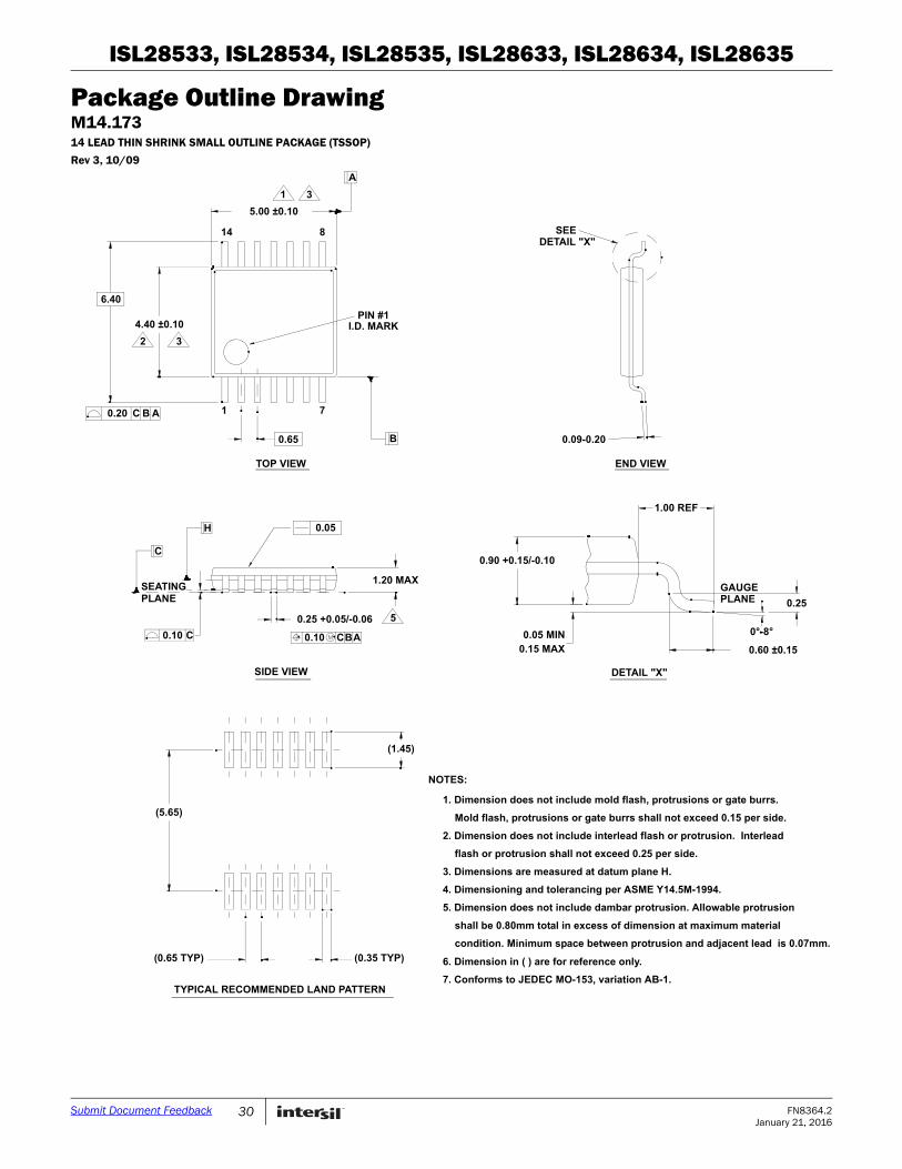
Package Outline Drawing . . . . . . . . . . . . . . . . . . . . . . . . . . . . . . . . . . . . . . . . . . . . . . . . . . . . . . . . . . . . . . . . . . . . . . . . . . . . . . . . . . . . 30
2 FN8364.2January 21, 2016
Submit Document Feedback

ISL28533, ISL28534, ISL28535, ISL28633, ISL28634, ISL28635
Pin ConfigurationsISL28533, ISL28534, ISL28535 SINGLE-ENDED OUTPUT
(14 LD TSSOP)TOP VIEW
ISL28633, ISL28634, ISL28635 DIFFERENTIAL OUTPUT(14 LD TSSOP)
TOP VIEW
Pin DescriptionsISL28533ISL28534ISL28535
(SINGLE-ENDED OUTPUT)
ISL28633ISL28634ISL28635
(DIFFERENTIAL OUTPUT) PIN
NAMEEQUIVALENT
CIRCUIT FUNCTION COMMENTS
4 4 INA+ Circuit 1 INA+ Input Positive Differential Input
5 5 INA- Circuit 1 INA- Input Negative Differential Input
12 - OUTA Circuit 2 INA Output Single Ended Output
- 12 OUTA+ Circuit 2 INA +Output Positive Differential Output
- 10 OUTA- Circuit 2 INA -Output Negative Differential Output
6 6 VA+ Circuit 1 A2 Output INA Gain Stage +Output
3 3 VA- Circuit 1 A1 Output INA Gain Stage -Output
11 11 REF Circuit 1 Output Reference INA Output Reference
1 1 G0 Circuit 1 Gain Control Logic Input
2 2 G1 Circuit 1 Gain Control Logic Input
8 - IN+ Circuit 1 Non-Inverting Op Amp Input Auxiliary Amplifier IN+
9 - IN- Circuit 1 Inverting Op Amp Input Auxiliary Amplifier IN-
10 - OUT Circuit 2 Op Amp Output Auxiliary Amplifier OUT
14 14 V+ Circuit 3 Positive supply Single Supply: +2.5V to +5.5VDual Supply: ±1.25V to ±2.75V
7 7 V- Circuit 3 Negative supply
- 8, 9 N.C. No Connect
13 13 DNC Do Not Connect Pin must float
1
2
3
4
G0
G1
VA-
INA+
-+
5
6
7
INA-
VA+
V-
10
9
8
11
12
13
14 V+
DNC
OUTA
REF
OUT
IN-
IN+
-+
1
2
3
4
G0
G1
VA-
INA+
5
6
7
INA-
VA+
V-
10
9
8
11
12
13
14 V+
DNC
OUTA+
REF
OUTA-
N.C.
N.C.
-+
V+
V-
OUT
CIRCUIT 2
V+
V-
CAPACITIVELYCOUPLED
ESD CLAMP
CIRCUIT 3
V+
V-
INA+,
INA-,
IN+,
IN-
CIRCUIT 1
3 FN8364.2January 21, 2016
Submit Document Feedback

ISL28533, ISL28534, ISL28535, ISL28633, ISL28634, ISL28635
Typical Sensor Application Block Diagram, ISL28533 Single-Ended Output
Typical Bridge Sensor Application Block Diagram, ISL28634 Differential Output
+
-
+
-
INA-
A2
A1
INA+
+
-
+
-
REF
OUTAA3
A4
RG
RG
IN+
IN-
OUT
VA-
VA+
20kΩ
20kΩ
20kΩ
20kΩ
ISL28533SENSOR
COMMONMODESENSE
ISL2632012-bit ADC
IN
ISL210905V VREF
ISL210902.5V VREF
VCC+5V
V+
REF+
OUT-
+
-
VCM
10kΩ
10kΩ
OUT+
VCC
V-
ISL28134
FIGURE 3. SENSOR APPLICATION WITH COMMON-MODE SENSING AND BUFFERED REFERENCE DRIVE
+
-
ISL28634
ISL2610424-BIT ADC
TO GUI
ISL21010
5V VREFR5F10JBC (RL78/G1C)
Renesas
+5V
350Ω
350Ω
FOIL STRAIN
350Ω
GAUGE 50Ω
50Ω
S
S
MICROCONTROLLER
+-
+-
VA+
VA-ISL28233
ISL23328
Gain Control
Ch 1
Ch 2
Ch 4
Ch 3
DCP
FIGURE 4. SIMPLIFIED STRAIN GAUGE SCHEMATIC
4 FN8364.2January 21, 2016
Submit Document Feedback

ISL28533, ISL28534, ISL28535, ISL28633, ISL28634, ISL28635
G0 and G1 Programmable Gain SettingG1
(NOTE)G0
(NOTE)ISL28533ISL28633
ISL28534ISL28634
ISL28535ISL28635
0 0 1 1 1
0 Z 2 2 100
0 1 4 10 120
Z 0 5 50 150
Z Z 10 100 180
Z 1 20 200 200
1 0 40 300 300
1 Z 50 500 500
1 1 100 1000 1000
APPLICATIONS
MedicalPiezo-Electric
Pressure SensorFluid Sensor
Shunt SenseOptical Sensors
Strain GaugeThermocouple
Strain Gauge
NOTE: For valid logic “Z” state leave G0/G1 pins in high impedance state. Internal 100kΩ pull-up and pull-down resistors on these pins establishes logic “Z”. See “Applications Information” on page 25 for more information.
Ordering InformationPART NUMBER(Notes 1, 2, 3)
PART MARKING
TEMP RANGE (°C)
PACKAGE(RoHS Compliant)
PKG. DWG. #
ISL28533FVZ 28533 FVZ -40 to +125 14 Ld TSSOP M14.173
ISL28534FVZ 28534 FVZ -40 to +125 14 Ld TSSOP M14.173
ISL28535FVZ 28535 FVZ -40 to +125 14 Ld TSSOP M14.173
ISL28633FVZ 28633 FVZ -40 to +125 14 Ld TSSOP M14.173
ISL28634FVZ 28634 FVZ -40 to +125 14 Ld TSSOP M14.173
ISL28635FVZ 28635 FVZ -40 to +125 14 Ld TSSOP M14.173
ISL28533EV2Z ISL28533 Evaluation Board
ISL28534EV2Z ISL28534 Evaluation Board
ISL28535EV2Z ISL28535 Evaluation Board
ISL28633EV2Z ISL28633 Evaluation Board
ISL28634EV2Z ISL28634 Evaluation Board
ISL28635EV2Z ISL28635 Evaluation Board
NOTES:
1. Add “-T13” suffix for 2.5k unit or “-T7A” suffix for 250 unit Tape and Reel options. Please refer to TB347 for details on reel specifications.
2. These Intersil Pb-free plastic packaged products employ special Pb-free material sets, molding compounds/die attach materials, and 100% matte tin plate plus anneal (e3 termination finish, which is RoHS compliant and compatible with both SnPb and Pb-free soldering operations). Intersil Pb-free products are MSL classified at Pb-free peak reflow temperatures that meet or exceed the Pb-free requirements of IPC/JEDEC J STD-020.
3. For Moisture Sensitivity Level (MSL), please see device information page for ISL28533, ISL28534, ISL28535, ISL28633, ISL28634, ISL28635. For more information on MSL please see tech brief TB363.
5 FN8364.2January 21, 2016
Submit Document Feedback

ISL28533, ISL28534, ISL28535, ISL28633, ISL28634, ISL28635
Absolute Maximum Ratings Thermal InformationSupply Voltage V+ to V- . . . . . . . . . . . . . . . . . . . . . . . . . . . . . . . . . . . . . . . . 6VInput Voltage VIN to GND . . . . . . . . . . . . . . . . . . ((V-) - 0.3V) to ((V+) + 0.3V)Input Differential Voltage . . . . . . . . . . . . . . . . . . . . . . . . . . . . . . . . . . V+ to V-Input Current . . . . . . . . . . . . . . . . . . . . . . . . . . . . . . . . . . . . . . . . . . . . . . 5mAOutput Current IOUT (10s) . . . . . . . . . . . . . . . . . . . . . . . . . . . . . . . . . . ±40mALatch-Up
Class 2 Level . . . . . . . . . . . . . . . . . . . . . . . . . . . . . . . . . . . . . . . . . . . 100mAESD Rating
Human Body Model . . . . . . . . . . . . . . . . . . . . . . . . . . . . . . . . . . . . . . . . 8kVMachine Model . . . . . . . . . . . . . . . . . . . . . . . . . . . . . . . . . . . . . . . . . . 700VCharged Device Model . . . . . . . . . . . . . . . . . . . . . . . . . . . . . . . . . . . . . . 2kV
Thermal Resistance (Typical) JA (°C/W) JC (°C/W)14 Ld TSSOP (Notes 4, 5) . . . . . . . . . . . . . . 92 30
Maximum Storage Temperature Range . . . . . . . . . . . . . -65°C to +150°CPb-Free Reflow Profile . . . . . . . . . . . . . . . . . . . . . . . . . . . . . . . . . . see TB493
Operating ConditionsTemperature Range . . . . . . . . . . . . . . . . . . . . . . . . . . . . . . -40°C to +125°CMaximum Junction Temperature . . . . . . . . . . . . . . . . . . . . . . . . . . . +140°CSupply Voltage . . . . . . . . . . . . . . . . . . . . . . 2.5V (±1.25V) to 5.5V (±2.75V)
CAUTION: Do not operate at or near the maximum ratings listed for extended periods of time. Exposure to such conditions may adversely impact productreliability and result in failures not covered by warranty.
NOTES:
4. JA is measured with the component mounted on a high effective thermal conductivity test board in free air. See Tech Brief TB379 for details.
5. For JC, the “case temp” location is taken at the package top center.
Electrical Specifications V+ = 5V, V- = 0V, VIN+ = VIN- = VREF = 2.5V, TA = +25°C, unless otherwise specified. Boldface limits apply across the operating temperature range, -40°C to +125°C.
PARAMETER DESCRIPTION TEST CONDITIONSMIN
(Note 6) TYPMAX
(Note 6) UNIT
POWER SUPPLY DC SPECIFICATIONS
VS Supply Voltage VS = (V+) - (V-) 2.5 - 5.5 V
IS Supply Current VS = 5V
ISL2853x, RL = OPEN - 2.9 3.4 mA
- - 3.5 mA
ISL2863x, RL = OPEN - 3.0 3.5 mA
- - 3.6 mA
5V DC SPECIFICATIONS INSTRUMENTATION AMPLIFIER
VOS, I Input Stage Offset Voltage +25°C -5.0 ±0.6 5.0 µV
-40°C to +85°C -9 - 9 µV
-40°C to +125°C -10 - 10 µV
TCVOS, I Input Stage Offset Voltage Temperature Coefficient
-40°C to +125°C -50 ±5 50 nV/°C
VOS, O Output Stage Offset Voltage +25°C -15 ±2 15 µV
-40°C to +85°C -45 - 45 µV
-40°C to +125°C -65 - 65 µV
TCVOS, O Output Stage Offset Voltage Temperature Coefficient
-40°C to +125°C -0.50 ±0.15 0.50 µV/°C
IB Input Bias Current +25°C -400 ±50 400 pA
-40°C to +85°C -400 - 400 pA
-40°C to +125°C -1 - 1 nA
IOS Input Offset Current +25°C -300 ±50 300 pA
-40°C to +85°C -350 - 350 pA
-40°C to +125°C -1 - 1 nA
ZIN Input Impedance Common-mode - 10 - GΩ
- 5 - pF
6 FN8364.2January 21, 2016
Submit Document Feedback

ISL28533, ISL28534, ISL28535, ISL28633, ISL28634, ISL28635
EGAIN Gain Error G = 1 to 50 -0.20 ±0.05 0.20 %
-0.35 - 0.35 %
G = 100 to 500 -0.30 ±0.05 0.30 %
-0.4 - 0.4 %
G = 1000 -0.40 ±0.05 0.40 %
-0.5 - 0.5 %
GAIN_TC Gain Drift G = 1 to 1,000-40°C to +125°C
- 10 - ppm/°C
GNL Gain Non-Linearity VOUT = +0.1V to +4.9V; RL = 10kΩ
G = 1 - 5 - ppm
G = 10 - 5 - ppm
G = 100 - 10 - ppm
G = 1000 - 10 - ppm
CMRR Common-Mode Rejection Ratio VCM = +0.1V to +4.9V
G = 1 80 100 - dB
G = 10 100 114 - dB
90 - - dB
G = 100 110 138 - dB
100 - - dB
G = 1000 120 150 - dB
110 - - dB
CMIR Common-Mode Input Range Guaranteed by CMRR (V-) + 0.1 - (V+) - 0.1 V
VREF Range Reference Voltage Range ISL2853x V- - V+ V
ISL2863x (V-) + 0.6 - (V+) - 1 V
IREF Reference Input Current ISL2853xVIN+ = VIN- = VREF = 2.5V
-0.5 0.1 0.5 µA
-1 - 1 µA
ISL2863xVREF = 2.5V
-500 150 500 pA
-25 - 25 nA
ZREF Reference Input Impedance ISL2853x 36 40 44 kΩ
ISL2863x - 10 - GΩ
PSRR Power Supply Rejection Ratio Vs = +2.5V to +5.5V
G = 1V/V 110 130 - dB
G = 10V/V 110 140 - dB
G = 100V/V 120 140 - dB
G = 1000V/V 120 140 - dB
ISC Short-Circuit Output Source Current RL = Short to V- - 45 - mA
Short-Circuit Output Sink Current RL = Short to V+ - -45 - mA
VOH High Output Voltage from V+((V+) - VOUT)
RL = 10kΩ V+ to VREF - 10 15 mV
- - 20 mV
Electrical Specifications V+ = 5V, V- = 0V, VIN+ = VIN- = VREF = 2.5V, TA = +25°C, unless otherwise specified. Boldface limits apply across the operating temperature range, -40°C to +125°C. (Continued)
PARAMETER DESCRIPTION TEST CONDITIONSMIN
(Note 6) TYPMAX
(Note 6) UNIT
7 FN8364.2January 21, 2016
Submit Document Feedback

ISL28533, ISL28534, ISL28535, ISL28633, ISL28634, ISL28635
VOL Low Output Voltage from V-((V-) + VOUT)
RL = 10kΩ V- to VREF - 10 15 mV
- - 20 mV
5V G0/G1 LOGIC INPUTS INSTRUMENTATION AMPLIFIER
VIH Logic Input High Threshold Vs = (V+) - (V-) 0.8 * (Vs) - - V
VIL Logic Input Low Threshold Vs = (V+) - (V-) - - 0.2 * (Vs) V
VIH_Z/VIL_Z Hi-Z Logic Input Range Vs = (V+) - (V-) 0.4 * (Vs) - 0.6 * (Vs) V
VOC Open Circuit Logic Voltage Set by 2 internal 100kΩ resistors;VS = (V+) - (V-)
0.45 * VS - 0.55 * VS V
ZIN Logic Input Impedance - 50k - kΩ
5V AC SPECIFICATIONS INSTRUMENTATION AMPLIFIER
eN Total Input Referred Voltage Noise eN = √(eNi2 + (eNo/G)2 + (IN*RS)2)
eNi Input Noise Voltage f = 0.1Hz to 10Hz; G = 100 - 0.4 - µVP-P
f = 1kHz; G = 100 - 17 - nV/√Hz
eNo Output Noise Voltage f = 0.1Hz to 10Hz; G = 1 - 1.8 - µVP-P
f = 1kHz; G = 1 - 65 - nV/√Hz
IN Input Noise Current f = 10Hz; RS = 5MΩ; G = 100 - 100 - fA/√Hz
GBWP Gain Bandwidth Product G ≥ 10 - 2.3 - MHz
G < 10 - 1.6 - MHz
5V TRANSIENT RESPONSE INSTRUMENTATION AMPLIFIER
SR Slew Rate20% to 80%
VOUT = 4VP-P; G = 1 - 0.8 - V/µs
VOUT = 4VP-P; G = 100 - 0.28 - V/µs
tGPD Gain Select Prop Delay All gains, 2V to 4V output after gain change
- 1 - µs
ts Settling Time To 0.1%, 4VP-P step - 20 - µs
To 0.01%, 4VP-P step - 70 - µs
trecover Output Overload Recovery Time, Recovery to 90% of Output Saturation
G = 1 - 1 - µs
5V DC SPECIFICATIONS OPERATIONAL AMPLIFIER
AvOPEN Open Loop Gain - 140 - dB
VOS Input Offset Voltage TA = +25°C -2.5 -0.2 2.5 µV
TA = -40°C to +85°C -3.475 - 3.475 µV
TA = -40°C to +125°C -4 - -4 µV
TCVOS Input Offset Voltage Temperature Coefficient
TA = -40°C to +125°C -15 -0.5 15 nV/°C
IB Input Bias Current TA = +25°C -300 ±15 300 pA
TA = -40°C to +85°C -300 - 300 pA
TA = -40°C to +125°C -550 - 550 pA
Electrical Specifications V+ = 5V, V- = 0V, VIN+ = VIN- = VREF = 2.5V, TA = +25°C, unless otherwise specified. Boldface limits apply across the operating temperature range, -40°C to +125°C. (Continued)
PARAMETER DESCRIPTION TEST CONDITIONSMIN
(Note 6) TYPMAX
(Note 6) UNIT
8 FN8364.2January 21, 2016
Submit Document Feedback

ISL28533, ISL28534, ISL28535, ISL28633, ISL28634, ISL28635
IOS Input Offset Current -600 ±50 600 pA
TA = -40°C to +85°C -600 - 600 pA
TA = -40°C to +125°C -1100 - 1100 pA
Common-Mode Input Voltage Range
V+ = 5.0V, V- = 0VGuaranteed by CMRR
0 - 5 V
CMRR Common-Mode Rejection Ratio VCM = 0V to 5V 110 135 - dB
97 - - dB
PSRR Power Supply Rejection Ratio VS = 2.5V to 5.5V 120 135 - dB
ISC Short-Circuit Output Source Current RL = Short to V- - 40 - mA
Short-Circuit Output Sink Current RL = Short to V+ - -40 - mA
VOH Output Voltage Swing, HIGHFrom VOUT to V+
RL = 10kΩto V- - 20 45 mV
RL = 10kΩto V- - - 50 mV
VOL Output Voltage Swing, LOWFrom V- to VOUT
RL = 10kΩto V+ - 20 45 mV
RL = 10kΩto V+ - - 50 mV
5V AC SPECIFICATIONS OPERATIONAL AMPLIFIER
CIN Input Capacitance Differential - 5.2 - pF
Common-mode - 5.6 - pF
eN Input Noise Voltage f = 0.1Hz to 10Hz - 0.25 - µVP-P
f = 1kHz - 10 - nV/Hz
IN Input Noise Current f = 1kHz - 200 - fA/Hz
GBWP Gain Bandwidth Product - 3 - MHz
Electrical Specifications V+ = 5V, V- = 0V, VIN+ = VIN- = VREF = 2.5V, TA = +25°C, unless otherwise specified. Boldface limits apply across the operating temperature range, -40°C to +125°C. (Continued)
PARAMETER DESCRIPTION TEST CONDITIONSMIN
(Note 6) TYPMAX
(Note 6) UNIT
Operating Specifications V+ = 2.5V, V- = 0V, VCM = 1.25V, TA = +25°C, unless otherwise specified. Boldface limits apply across the operating temperature range, -40°C to +125°C.
PARAMETER DESCRIPTION TEST CONDITIONSMIN
(Note 6) TYPMAX
(Note 6) UNIT
2.5V DC SPECIFICATIONS INSTRUMENTATION AMPLIFIER
VOS, I Input Stage Offset Voltage +25°C -5.0 ±0.6 5.0 µV
-40°C to +85°C -9 - 9 µV
-40°C to +125°C -10 - 10 µV
TCVOS, I Input Stage Offset Voltage Temperature Coefficient
-40°C to +125°C -50 ±5 50 nV/°C
VOS, O Output Stage Offset Voltage +25°C -15 ±2 15 µV
-40°C to +85°C -45 - 45 µV
-40°C to +125°C -65 - 65 µV
TCVOS, O Output Stage Offset Voltage Temperature Coefficient
-40°C to +125°C -0.50 ±0.15 0.50 µV/°C
IB Input Bias Current +25°C -400 ±50 400 pA
-40°C to +85°C -400 - 400 pA
-40°C to +125°C -1 - 1 nA
9 FN8364.2January 21, 2016
Submit Document Feedback

ISL28533, ISL28534, ISL28535, ISL28633, ISL28634, ISL28635
IOS Input Offset Current +25°C -300 ±50 300 pA
-40°C to +85°C -350 - 350 pA
-40°C to +125°C -1 - 1 nA
ZIN Input Impedance Common-mode - 10 - GΩ
- 5 - pF
EGAIN Gain Error G = 1 to 50 -0.20 ±0.05 0.20 %
-0.35 - 0.35 %
G = 100 to 500 -0.30 ±0.05 0.30 %
-0.4 - 0.4 %
G = 1000 -0.40 ±0.05 0.40 %
-0.5 - 0.5 %
GAIN_TC Gain Drift G = 1 to 1,000-40°C to +125°C
- 10 - ppm/°C
CMRR Common-Mode Rejection Ratio VCM = +0.1V to +2.4V
G = 1 80 100 - dB
G = 10 100 114 - dB
90 - - dB
G = 100 110 138 - dB
100 - - dB
G = 1000 120 150 - dB
110 - - dB
CMIR Common-Mode Input Range Guaranteed by CMRR (V-) + 0.1 - (V+) - 0.1 V
VREF Range Reference Voltage Range ISL2853x V- - V+ V
ISL2863x (V-) + 0.6 - (V+) - 1 V
IREF Reference Input Current ISL2853xVIN+ = VIN- = VREF = 1.25V
-0.5 0.1 0.5 µA
-1 - 1 µA
ISL2863x -500 150 500 pA
-25 - 25 nA
ZREF Reference Input Impedance ISL2853x 36 40 44 kΩ
ISL2863x - 10 - GΩ
PSRR Power Supply Rejection Ratio Vs = +2.5V to +5.5V
G = 1V/V 110 130 - dB
G = 10V/V 110 140 - dB
G = 100V/V 120 140 - dB
G = 1000V/V 120 140 - dB
ISC Short-Circuit Output Source Current RL = Short to V- - 25 - mA
Short-Circuit Output Sink Current RL = Short to V+ - -25 - mA
VOH Output Voltage Swing, HIGH RL = 10kΩ to VREF - 5 15 mV
- - 20 mV
Operating Specifications V+ = 2.5V, V- = 0V, VCM = 1.25V, TA = +25°C, unless otherwise specified. Boldface limits apply across the operating temperature range, -40°C to +125°C. (Continued)
PARAMETER DESCRIPTION TEST CONDITIONSMIN
(Note 6) TYPMAX
(Note 6) UNIT
10 FN8364.2January 21, 2016
Submit Document Feedback
ISL28533, ISL28534, ISL28535, ISL28633, ISL28634, ISL28635
VOL Output Voltage Swing, LOW RL = 10kΩ to VREF - 5 15 mV
- - 20 mV
2.5V G0/G1 LOGIC INPUTS INSTRUMENTATION AMPLIFIER
VIH Logic Input High Threshold Vs = (V+) - (V-) 0.8 * (Vs) - - V
VIL Logic Input Low Threshold Vs = (V+) - (V-) - - 0.2 * (Vs) V
VIH_Z/VIL_Z Hi-Z Logic Input Range Vs = (V+) - (V-) 0.4 * (Vs) - 0.6 * (Vs) V
VOC Open Circuit Logic Voltage Set by 2 internal 100kΩ Resistors;VS = (V+) - (V-)
0.45 * VS - 0.55 * VS V
ZIN Logic Input Impedance - 50k - kΩ
2.5V AC SPECIFICATIONS INSTRUMENTATION AMPLIFIER
eN Total Input Referred Voltage Noise eN = √(eNi2 + (eNo/G)2 + (IN*RS)2)
eNi Input Noise Voltage f = 0.1Hz to 10Hz; G = 100 - 0.4 - µVP-P
f = 1kHz; G = 100 - 17 - nV/√Hz
eNo Output Noise Voltage f = 0.1Hz to 10Hz; G = 1 - 1.8 - µVP-P
f = 1kHz; G = 1 - 65 - nV/√Hz
IN Input Noise Current f = 10Hz; RS = 5MΩ; G = 100 - 100 - fA/√Hz
GBWP Gain Bandwidth Product G ≥ 10 - 2.3 - MHz
G < 10 - 1.6 - MHz
2.5V TRANSIENT RESPONSE INSTRUMENTATION AMPLIFIER
SR Slew Rate10% to 90%
VOUT = 2VP-P; G = 1 - 0.8 - V/µs
VOUT = 2VP-P; G = 100 - 0.1 - V/µs
tGPD Gain Select Prop Delay All gains - 1 - µs
ts Settling Time to 0.1%, 4VP-P Step To 0.1%, 2VP-P step - 20 - µs
To 0.01%, 2VP-P step - 70 - µs
trecover Output Overload Recovery Time, Recovery to 90% of output saturation
- 1.5 - µs
2.5V DC SPECIFICATIONS OPERATIONAL AMPLIFIER
AvOPEN Open Loop Gain - 140 - dB
VOS Input Offset Voltage TA = +25°C -2.5 -0.2 2.5 µV
TA = -40°C to +85°C -3.475 - 3.475 µV
TA = -40°C to +125°C -4 - -4 µV
TCVOS Input Offset Voltage Temperature Coefficient
TA = -40°C to +125°C -15 -0.5 15 nV/°C
IB Input Bias Current TA = +25°C -300 ±15 300 pA
TA = -40°C to +85°C -300 - 300 pA
TA = -40°C to +125°C -550 - 550 pA
Operating Specifications V+ = 2.5V, V- = 0V, VCM = 1.25V, TA = +25°C, unless otherwise specified. Boldface limits apply across the operating temperature range, -40°C to +125°C. (Continued)
PARAMETER DESCRIPTION TEST CONDITIONSMIN
(Note 6) TYPMAX
(Note 6) UNIT
11 FN8364.2January 21, 2016
Submit Document Feedback

ISL28533, ISL28534, ISL28535, ISL28633, ISL28634, ISL28635
IOS Input Offset Current TA = +25°C -600 ±50 600 pA
TA = -40°C to +85°C -600 - 600 pA
TA = -40°C to +125°C -1100 - 1100 pA
Common-Mode Input Voltage Range
V+ = 2.5V, V- = 0VGuaranteed by CMRR
0 - 2.5 V
CMRR Common-Mode Rejection Ratio VCM = 0V to 2.5V 110 135 - dB
97 - - dB
PSRR Power Supply Rejection Ratio Vs = 2.5V to 5.5V 120 135 - dB
ISC Short-Circuit Output Source Current RL = Short to V- - 25 - mA
Short-Circuit Output Sink Current RL = Short to V+ - -25 - mA
VOH Output Voltage Swing, HIGHFrom VOUT to V+
RL = 10kΩto VCM - 10 20 mV
RL = 10kΩto VCM - - 25 mV
VOL Output Voltage Swing, LOWFrom V- to VOUT
RL = 10kΩto VCM - 10 20 mV
RL = 10kΩto VCM - - 25 mV
2.5V AC SPECIFICATIONS OPERATIONAL AMPLIFIER
CIN Input Capacitance Differential - 5.2 - pF
Common-mode - 5.6 - pF
eN Input Noise Voltage f = 0.1Hz to 10Hz - 0.25 - µVP-P
f = 1kHz - 10 - nV/Hz
IN Input Noise Current f = 1kHz - 200 - fA/Hz
GBWP Gain Bandwidth Product - 3 - MHz
NOTE:6. Compliance to data sheet limits are assured by one or more methods: production test, characterization and/or design.
Operating Specifications V+ = 2.5V, V- = 0V, VCM = 1.25V, TA = +25°C, unless otherwise specified. Boldface limits apply across the operating temperature range, -40°C to +125°C. (Continued)
PARAMETER DESCRIPTION TEST CONDITIONSMIN
(Note 6) TYPMAX
(Note 6) UNIT
12 FN8364.2January 21, 2016
Submit Document Feedback
ISL28533, ISL28534, ISL28535, ISL28633, ISL28634, ISL28635
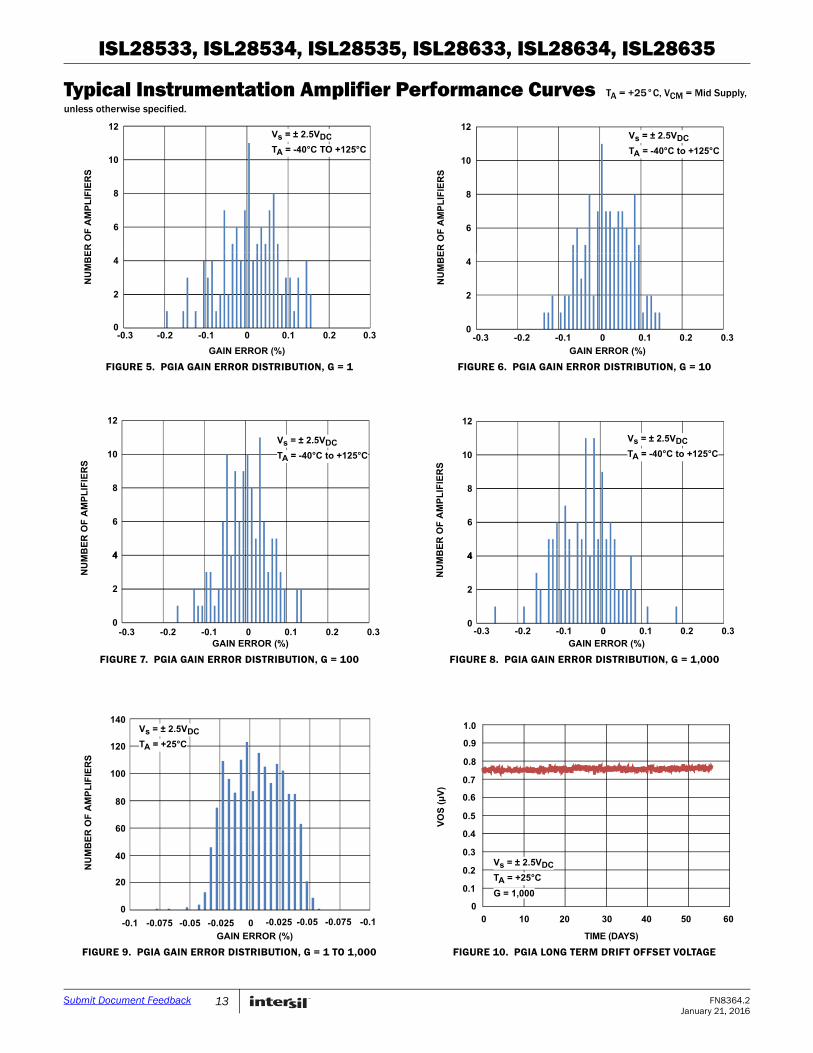
Typical Instrumentation Amplifier Performance Curves TA = +25°C, VCM = Mid Supply,
unless otherwise specified.
FIGURE 5. PGIA GAIN ERROR DISTRIBUTION, G = 1 FIGURE 6. PGIA GAIN ERROR DISTRIBUTION, G = 10
FIGURE 7. PGIA GAIN ERROR DISTRIBUTION, G = 100 FIGURE 8. PGIA GAIN ERROR DISTRIBUTION, G = 1,000
FIGURE 9. PGIA GAIN ERROR DISTRIBUTION, G = 1 TO 1,000 FIGURE 10. PGIA LONG TERM DRIFT OFFSET VOLTAGE
NU
MB
ER
OF
AM
PL
IFIE
RS
GAIN ERROR (%)
6
8
10
12
0
2
4
-0.3 -0.2 -0.1 0 0.1 0.2 0.3
Vs = ± 2.5VDC
TA = -40°C TO +125°C
NU
MB
ER
OF
AM
PL
IFIE
RS
GAIN ERROR (%)
6
8
10
12
0
2
4
-0.3 -0.2 -0.1 0 0.1 0.2 0.3
Vs = ± 2.5VDC
TA = -40°C to +125°C
NU
MB
ER
OF
AM
PL
IFIE
RS
GAIN ERROR (%)
4
6
8
10
12
0
2
4
-0.3 -0.2 -0.1 0 0.1 0.2 0.3
Vs = ± 2.5VDC
TA = -40°C to +125°C
NU
MB
ER
OF
AM
PL
IFIE
RS
GAIN ERROR (%)
4
6
8
10
12
0
2
4
-0.3 -0.2 -0.1 0 0.1 0.2 0.3
Vs = ± 2.5VDC
TA = -40°C to +125°C
NU
MB
ER
OF
AM
PL
IFIE
RS
GAIN ERROR (%)
80
100
120
0
20
40
60
-0.1 -0.075 -0.05 -0.025 0
140
-0.1-0.075-0.05-0.025
Vs = ± 2.5VDC
TA = +25°C
00 10 20 30 40 50 60
VO
S (
µV
)
TIME (DAYS)
0.4
0.5
0.6
0.1
0.2
0.3
0.7
0.8
0.9
1.0
Vs = ± 2.5VDC
TA = +25°C
G = 1,000
13 FN8364.2January 21, 2016
Submit Document Feedback

ISL28533, ISL28534, ISL28535, ISL28633, ISL28634, ISL28635
FIGURE 11. PGIA INPUT OFFSET VOLTAGE DISTRIBUTION FIGURE 12. PGIA OUTPUT OFFSET VOLTAGE DISTRIBUTION
FIGURE 13. PGIA RTI VOS vs COMMON-MODE VOLTAGE FIGURE 14. PGIA RTI VOS vs COMMON-MODE VOLTAGE
FIGURE 15. PGIA INPUT BIAS CURRENT vs TEMPERATURE FIGURE 16. PGIA IOS vs TEMPERATURE
Typical Instrumentation Amplifier Performance Curves TA = +25°C, VCM = Mid Supply,
unless otherwise specified. (Continued)
NU
MB
ER
OF
AM
PL
IFIE
RS
VOSI (µV)
20
25
30
0
5
10
15
-2.0 -1.6 -1.2 -0.8 -0.4 0 0.4 0.8 1.2 1.6 2.0
Vs = ± 2.5VDC
NU
MB
ER
OF
AM
PL
IFIE
RS
VOSO (µV)
6
8
10
12
14
0
2
4
-10 -8 -6 0 2 4 10
Vs = ± 2.5VDC
-4 -2 6 8
16
18
INPUT COMMOM-MODE VOLTAGE(V)
-2
0
2
4
6
-6
-4
-2
-2.0 -1.5 -1.0 -0.5 0 0.5 1.0 1.5 2.0
Vs = ± 1.25VDC
VO
S (
µV
)
VO
S (
µV
)
INPUT COMMON-MODE VOLTAGE (V)
-2
0
2
4
6
-6
-4
-3.0 -2.5 -2.0 -1.5 -1.0 -0.5 0 0.5 1.0 1.5 2.0 2.5 3.0
Vs = ± 2.5VDC
80
100
120
140
160
180
200
0
20
40
60
-50 -25 0 25 50 75 100 125 150
INP
UT
BIA
S C
UR
RE
NT
(p
A)
TEMPERATURE (°C)
IB+, VS = 5V
IB-, VS = 2.5V
IB+, VS = 2.5VIB-, VS = 5V
-50
0
50
100
150
200
-200
-150
-100
-50 -25 0 25 50 75 100 125 150
I OS
(p
A)
TEMPERATURE (°C)
IOS, VS = 5V
IOS, VS = 2.5V
14 FN8364.2January 21, 2016
Submit Document Feedback

ISL28533, ISL28534, ISL28535, ISL28633, ISL28634, ISL28635
FIGURE 17. PGIA INPUT COMMON-MODE RANGE vs OUTPUT VOLTAGE
FIGURE 18. PGIA INPUT COMMON-MODE RANGE vs OUTPUT VOLTAGE
FIGURE 19. PGIA INPUT COMMON-MODE RANGE vs OUTPUT VOLTAGE
FIGURE 20. PGIA INPUT COMMON-MODE RANGE vs DIFFERENTIAL OUTPUT VOLTAGE
FIGURE 21. PGIA CMRR vs TEMPERATURE FIGURE 22. PGIA PSRR vs TEMPERATURE
Typical Instrumentation Amplifier Performance Curves TA = +25°C, VCM = Mid Supply,
unless otherwise specified. (Continued)
OUTPUT VOLTAGE (V)
CO
MM
ON
-MO
DE
VO
LTA
GE
(V
)
0
1
2
3
-3
-2
-1
-3 -2 -1 0 1 2 3
Vs = ± 2. 5VDCVREF = 0V
ISL2853x
OUTPUT VOLTAGE (V)
CO
MM
ON
-MO
DE
VO
LTA
GE
(V
)
0
1
2
3
-3
-2
-1
-3 -2 -1 0 1 2 3
Vs = ± 2. 5VDCVREF = +2.5V
ISL2853x
OUTPUT VOLTAGE (V)
CO
MM
ON
-MO
DE
VO
LTA
GE
(V
)
0
1
2
3
-3
-2
-1
-3 -2 -1 0 1 2 3
Vs = ± 2. 5VDCVREF = -2.5V
ISL2853x
0
1
2
3
-3
-2
-1
-6 -4 -2 0 2 4 6
Vs = ± 2. 5VDCVREF = 0V
ISL2863x
VOUT+ TO VOUT- (V)
CO
MM
ON
-MO
DE
VO
LTA
GE
(V
)
TEMPERATURE (°C)
CM
RR
(d
B)
80
100
120
140
160
180
0
20
40
60
-50 -25 0 25 50 75 100 125 150
Vs = ± 2. 5VDC
G = 1G = 10G = 100
G = 1000
TEMPERATURE (°C)
PS
RR
(d
B)
60
80
100
120
140
160
180
0
20
40
60
-50 -25 0 25 50 75 100 125 150
G = 1G = 10G = 100
G = 1000
Vs = ± 2. 5VDC
15 FN8364.2January 21, 2016
Submit Document Feedback

ISL28533, ISL28534, ISL28535, ISL28633, ISL28634, ISL28635
FIGURE 23. PGIA OUTPUT VOLTAGE SWING vs OUTPUT CURRENT, ISL2853x
FIGURE 24. PGIA OUTPUT VOLTAGE SWING vs OUTPUT CURRENT, ISL2863x
FIGURE 25. PGIA OUTPUT VOLTAGE SWING vs OUTPUT CURRENT, ISL2853x
FIGURE 26. PGIA OUTPUT VOLTAGE SWING vs OUTPUT CURRENT, ISL2863x
FIGURE 27. SUPPLY CURRENT vs SUPPLY VOLTAGE vs TEMPERATURE FIGURE 28. PGIA VOH AND VOL vs TEMPERATURE
Typical Instrumentation Amplifier Performance Curves TA = +25°C, VCM = Mid Supply,
unless otherwise specified. (Continued)
0.01
0.1
1
0.0001
0.001
LOAD CURRENT (mA)
VO
LTA
GE
DR
OP
FR
OM
RA
IL (
V)
0.01 0.1 1 10010
VOLVs = +3V
VOH
LOAD CURRENT (mA)
VO
LTA
GE
DR
OP
FR
OM
RA
IL (
V)
0.1
1
0.001
0.01
Vs = +3V
0.01 0.1 1 10010
VOL
VOH
LOAD CURRENT (mA)
VO
LTA
GE
DR
OP
FR
OM
RA
IL (
V)
0.1
1
0.001
0.01
0.01 0.1 1 10010
Vs = +5V
VOH
VOL
LOAD CURRENT (mA)
VO
LTA
GE
DR
OP
FR
OM
RA
IL (
V)
0.1
1
0.001
0.01
0.01 0.1 1 10010
Vs = +5V
VOL
VOH
2.8
3.0
3.2
3.4
3.6
3.8
4.0
2.0
2.2
2.4
2.6
2.0 2.5 3.0 3.5 4.0 4.5 5.0 5.5 6.0
T = -40°C
T = +25°C
T = +85°C
T = +125°C
SU
PP
LY C
UR
RE
NT
(m
A)
SUPPLY VOLTAGE VS (V)
6
8
10
12
0
2
4
-50 -25 0 25 50 75 100 125 150
VOH 5VVOL 5V
VOH 2.5VVOL 2.5V
VO
H A
ND
VO
L V
OLT
AG
E (
mV
)
TEMPERATURE (°C)
16 FN8364.2January 21, 2016
Submit Document Feedback

ISL28533, ISL28534, ISL28535, ISL28633, ISL28634, ISL28635
FIGURE 29. PGIA 0.1Hz TO 10Hz NOISE FIGURE 30. PGIA 0.1Hz TO 10Hz NOISE
FIGURE 31. PGIA VOLTAGE NOISE SPECTRAL DENSITY vs FREQUENCY, 1Hz TO 100kHz
FIGURE 32. PGIA VOLTAGE NOISE SPECTRAL DENSITY vs FREQUENCY, 1Hz TO 100kHz
FIGURE 33. PGIA CURRENT NOISE SPECTRAL DENSITY 1Hz TO 100kHz, ISL2853x
FIGURE 34. PGIA CURRENT NOISE SPECTRAL DENSITY 1Hz TO 100kHz, ISL2863x
Typical Instrumentation Amplifier Performance Curves TA = +25°C, VCM = Mid Supply,
unless otherwise specified. (Continued)
VO
LTA
GE
NO
ISE
PE
AK
-TO
-PE
AK
(µV
)
TIME (s)
1 102 3 4 5 6 7 8 90
-3
-2
-1
1
2
3
Vs = ±2.5V
G = 1
0
-4
4
TIME (s)
1 102 3 4 5 6 7 8 90
Vs = ±2.5V
G = 1000
-0.3
-0.2
-0.1
0.1
0.2
0.3
0
-0.4
0.4
-0.5
0.5
VO
LTA
GE
NO
ISE
PE
AK
-TO
-PE
AK
(µV
)
VO
LTA
GE
NO
ISE
(n
V/√
Hz)
FREQUENCY (Hz)
1 10 100 1000 10k 100k1
10
100
1k
10k
100k
Vs = ±2.5V
ISL2853x
G = 1
G = 100 VO
LTA
GE
NO
ISE
(n
V/√
Hz)
FREQUENCY (Hz)
1 10 100 1000 10k 100k1
10
100
Vs = ±2.5V
1k
10k
100k
ISL2863x
G = 1
G = 100
VS = ±2.5VRS = 5MΩ
1 10 100 1k 10k 100k
FREQUENCY (Hz)
CU
RR
EN
T N
OIS
E (
fA/√
Hz)
1
0.1
10
100
1k
10k
G = 1
G = 100
Roll off from CSOURCE
ISL2853x
1 10 100 1k 10k 100k
1
0.1
10
100
1k
10k
CU
RR
EN
T N
OIS
E (
fA/√
Hz)
FREQUENCY (Hz)
VS = ±2.5VRS = 5MΩ
Roll off from CSOURCE
ISL2863x
G = 1
G = 100
17 FN8364.2January 21, 2016
Submit Document Feedback

ISL28533, ISL28534, ISL28535, ISL28633, ISL28634, ISL28635
FIGURE 35. PGIA GAIN VS FREQUENCY vs GAIN SETTINGS FIGURE 36. PGIA CMRR vs FREQUENCY
FIGURE 37. PGIA POSITIVE PSRR vs FREQUENCY FIGURE 38. PGIA NEGATIVE PSRR vs FREQUENCY
FIGURE 39. PGIA GAIN vs FREQUENCY vs CL, ISL2853x FIGURE 40. PGIA GAIN vs FREQUENCY vs CL, ISL2863x
Typical Instrumentation Amplifier Performance Curves TA = +25°C, VCM = Mid Supply,
unless otherwise specified. (Continued)
10 100 1k 10k 100k 1M
FREQUENCY (Hz)
GA
IN (
dB
)
10M
20
30
40
50
60
70
-10
0
10
100050030020010050202010421
Vs = ± 2. 5VRL = 10kΩ
60
80
100
120
140
160
0
20
40
60CM
RR
(d
B)
FREQUENCY (Hz)
10 100 1k 10M1M10k 100k
G = 100
G = 10
G = 1
Vs = ± 2. 5VDC
G = 1000
PO
SIT
IVE
PS
RR
(d
B)
FREQUENCY (Hz)
80
100
120
140
160
0
20
40
60
10 100 1k 10M1M10k 100k
G = 1
G = 10
Vs = ± 2. 5VDC
G = 100
FREQUENCY (Hz)
60
80
100
120
140
0
20
40
10 100 1k 10M1M10k 100k
NE
GA
TIV
E P
SR
R (
dB
)
G = 100
G = 1
G = 10
Vs = ± 2. 5VDC
FREQUENCY (Hz)
3
5
7
9
11
13
-5
-3
-1
1
1k 10k 100k 10M1M
1000pF
470pF
3300pF
4700pF
2200pF
Vs = ± 2. 5VDC
VOUT = 100mVP-P
AV = 1VRL = 10k
GA
IN (
dB
)
FREQUENCY (Hz)
GA
IN (
dB
)
1
3
5
7
9
11
-5
-3
-1
1470pF
3300pF
4700pF
2200pF
1000pF
1k 10k 100k 10M1M
Vs = ± 2. 5VDC
VOUT = 10mVP-P
AV = 1VRL = 10k
18 FN8364.2January 21, 2016
Submit Document Feedback

ISL28533, ISL28534, ISL28535, ISL28633, ISL28634, ISL28635
FIGURE 41. PGIA SMALL SIGNAL PULSE RESPONSE, G = 1, ISL2853x FIGURE 42. PGIA SMALL SIGNAL PULSE RESPONSE, G = 1, ISL2863x
FIGURE 43. PGIA LARGE SIGNAL PULSE RESPONSE, G = 1, 2, 10 ISL2853x
FIGURE 44. PGIA LARGE SIGNAL PULSE RESPONSE, G = 1, 2, 10 ISL2863x
FIGURE 45. PGIA LARGE SIGNAL PULSE RESPONSE, G = 1000, ISL2853x
FIGURE 46. PGIA LARGE SIGNAL PULSE RESPONSE, G = 1000, ISL2863x
Typical Instrumentation Amplifier Performance Curves TA = +25°C, VCM = Mid Supply,
unless otherwise specified. (Continued)
TIME (µs)
VO
LTA
GE
(V
)
-10 0 10 20 30 40
-0.02
0
0.02
0.04
0.06
0.08
0.10
-0.10
-0.08
-0.06
-0.04
Vs = ± 2. 5VDCRL = OPENVOUT = 100mVP-P
0
0.02
0.04
0.06
-0.06
-0.04
-0.02
TIME (µs)-10 0 10 20 30 40-5 5 15 25 35
Vs = ± 2. 5VDCRL = OPENVOUT = 100mVP-P
VO
UT
+ T
O V
OU
T- (
V)
TIME (µs)
VO
LTA
GE
(V
)
-10 0 10 20 30 40
-1
0
1
2
3
-3
-2
G = 10
G = 2
Vs = ± 2. 5VDCRL = OPENVOUT = 4VP-P
G = 1
TIME (µs)
-1
0
1
2
3
-3
-2
-20 -10 10 20 30 400
AV = 2
Vs = ± 2. 5VDCRL = OPENVOUT = 4VP-P
VO
UT
+ T
O V
OU
T- (
V)
AV = 1
AV = 10
TIME (µs)
-400 -200 200 400 800 10000 600
-0.5
0
0.5
1.0
1.5
2.0
2.5
-2.5
-2.0
-1.5
-1.0 Vs = ± 2. 5VDCRL = OPENVOUT = 4VP-P
VO
LTA
GE
(V
)
TIME (µs)
VO
UT
+ T
O V
OU
T- (
V)
-0.5
0
0.5
1.0
1.5
2.0
2.5
-2.5
-2.0
-1.5
-1.0
-400 -200 200 400 800 10000 600
Vs = ± 2. 5VDCRL = OPENVOUT = 4VP-P
19 FN8364.2January 21, 2016
Submit Document Feedback

ISL28533, ISL28534, ISL28535, ISL28633, ISL28634, ISL28635
FIGURE 47. CAPACITIVE LOAD OVERSHOOT; ISL2853x FIGURE 48. CAPACITIVE LOAD OVERSHOOT; ISL2863x
FIGURE 49. POSITIVE OVERLOAD RECOVERY TIME, ISL2853x FIGURE 50. POSITIVE OVERLOAD RECOVERY TIME, ISL2863x
FIGURE 51. NEGATIVE OVERLOAD RECOVERY TIME, ISL2853x FIGURE 52. NEGATIVE OVERLOAD RECOVERY TIME, ISL2863x
Typical Instrumentation Amplifier Performance Curves TA = +25°C, VCM = Mid Supply,
unless otherwise specified. (Continued)
-0.02
0
0.02
0.04
0.06
0.08
0.10
-0.08
-0.06
-0.04
OU
TP
UT
VO
LTA
GE
(V
)
TIME (µs)
-10 10 500 20 30 40
0pF100pF300pF500pF800pF1000pF
-0.06
-0.04
-0.02
0
0.02
0.04
0.06
-0.16
-0.14
-0.12
-0.10
-0.08
OU
TP
UT
VO
LTA
GE
(V
)
TIME (µs)
-10 10 600 20 30 5040
0pF OUT+0pF OUT-100pF OUT+100pF OUT-300pF OUT+300pF OUT-500pF OUT+500pF OUT-800pF OUT+800pF OUT-1nF OUT+1nF OUT-
-3
-2
-1
0
1
2
3
TIME (µs)
0 6 10 16 202 4 8 12 14 18
G = 100
G = 1
G = 10
INP
UT
AN
D O
UT
PU
T V
OLT
AG
E (
V)
VIN
-2
0
2
4
6
-6
-4
TIME (µs)
0 60 140 18020 40 80 100 120 160
VIN
G = 100
G = 1
G = 10
INP
UT
AN
D O
UT
PU
T V
OLT
AG
E (
V)
-1
0
1
2
3
-3
-2
-1
TIME (µs)
0 4 142 6 8 10 12
G = 100INP
UT
AN
D O
UT
PU
T V
OLT
AG
E (
V)
G = 1VIN
G = 10-2
0
2
4
6
-6
-4
TIME (µs)
VIN
G = 100
INP
UT
AN
D O
UT
PU
T V
OLT
AG
E (
V)
0 60 140 18020 40 80 100 120 160
G = 1
G = 10
20 FN8364.2January 21, 2016
Submit Document Feedback

ISL28533, ISL28534, ISL28535, ISL28633, ISL28634, ISL28635
FIGURE 53. CHANNEL SEPARATION vs FREQUENCY, HOSTILE INA, MONITOR OPAMP
FIGURE 54. CHANNEL SEPARATION vs FREQUENCY, HOSTILE OPAMP, MONITOR INA
Typical Instrumentation Amplifier Performance Curves TA = +25°C, VCM = Mid Supply,
unless otherwise specified. (Continued)
CH
AN
NE
L S
EP
AR
AT
ION
(d
B)
60
80
100
120
140
0
20
40
FREQUENCY (Hz)
10 100 1k 10M1M10k 100k
Op amp AV = 1
60
80
100
120
140
0
20
40
CH
AN
NE
L S
EP
AR
AT
ION
(d
B)
FREQUENCY (Hz)
10 100 1k 10M1M10k 100k
INA G = 1
INA G = 100
INA G = 10
21 FN8364.2January 21, 2016
Submit Document Feedback

ISL28533, ISL28534, ISL28535, ISL28633, ISL28634, ISL28635
Typical Operational Amplifier Performance Curves TA = +25°C, VCM = Mid Supply, unless
otherwise specified.
FIGURE 55. OP AMP VOS vs COMMON-MODE FIGURE 56. OP AMP VOS vs COMMON-MODE
FIGURE 57. OP AMP BIAS CURRENT vs TEMPERATURE FIGURE 58. OP AMP VOH AND VOL vs TEMPERATURE
FIGURE 59. OP AMP OUTPUT VOLTAGE SWING vs OUTPUT CURRENT FIGURE 60. OP AMP OUTPUT VOLTAGE SWING vs OUTPUT CURRENT
INPUT COMMON-MODE VOLTAGE (V)
-2
0
2
4
6
8
10
-10
-8
-6
-4
-2 -1.5 -1 -0.5 0 0.5 1 1.5 2
Vs = ± 1.25VDC
VO
S (
µV
)
AV= 100
INPUT COMMON-MODE VOLTAGE (V)
VO
S (
µV
)
-2
0
2
4
6
8
10
-10
-8
-6
-4
-3.0 -2.5 -2.0 -1.5 -1.0 -0.5 0 0.5 1.0 1.5 2.0 2.5 3.0
Vs = ± 2.5VDCAV= 100
-100
0
100
200
300
400
-400
-300
-200
-50 -25 0 25 50 75 100 125 150
INP
UT
BIA
S C
UR
RE
NT
(p
A)
IB+, VS = 5V
IB-, VS = 5V
IB-, VS = 2.5V
TEMPERATURE (°C)
IB+, VS = 2.5V
15
20
25
30
35
0
5
10
-50 0 50 100 150
VO
H A
ND
VO
L V
OLT
AG
E (
mV
)
TEMPERATURE (°C)
VOL = 5V
VOH = 5V
VOH = 2.5VVOL = 2.5V
0.1
1
0.001
0.01
LOAD CURRENT (mA)
Vs = +5VDC
0.01 0.1 1 10010
VO
LTA
GE
DR
OP
FR
OM
RA
IL (
V)
VOH
VOL
0.01
0.1
1
0.0001
0.001
LOAD CURRENT (mA)
Vs = +3VDC
0.01 0.1 1 10010
VO
LTA
GE
DR
OP
FR
OM
RA
IL (
V)
VOH
VOL
22 FN8364.2January 21, 2016
Submit Document Feedback

ISL28533, ISL28534, ISL28535, ISL28633, ISL28634, ISL28635
FIGURE 61. OP AMP GAIN vs FREQUENCY FIGURE 62. OP AMP CAPACITIVE LOAD vs FREQUENCY
FIGURE 63. OP AMP POWER SUPPLY REJECTION RATIO FIGURE 64. OP AMP POWER SUPPLY REJECTION RATIO
FIGURE 65. OP AMP SMALL SIGNAL TRANSIENT RESPONSE FIGURE 66. OP AMP LARGE SIGNAL TRANSIENT RESPONSE
Typical Operational Amplifier Performance Curves TA = +25°C, VCM = Mid Supply, unless
otherwise specified. (Continued)
GA
IN (
dB
)
FREQUENCY (Hz)
10 100 1k 10M1M10k 100k
30
40
50
60
70
80
-10
0
10
20
AV = 1000
AV = 100
AV = 10
AV = 1
RG = 10k, RF = 100k
RG = 1k, RF = 100k
RG = 100, RF = 100k
RG = OPEN, RF = 0
Vs = ± 2. 5VRL = 10kΩ
FREQUENCY (Hz)
GA
IN (
dB
)
2
4
6
8
10
12
14
-6
-4
-2
0
2
1k 10M1M10k 100k
0pF
470pF
1000pF
100pF
Vs = ± 2. 5VRL = 10kΩAV = 1
47pF
60
80
100
120
0
20
40
NE
GA
TIV
E P
SR
R (
dB
)
FREQUENCY (Hz)
10 100 1k 10M1M10k 100k
Vs = ± 2. 5VDCAV = 1
60
80
100
120
140
0
20
40PO
SIT
IVE
PS
RR
(d
B)
FREQUENCY (Hz)
10 100 1k 10M1M10k 100k
Vs = ± 2. 5VDCAV = 1
TIME (µs)
OU
TP
UT
VO
LTA
GE
(V
)
-1 0 1 3 4
-0.02
0
0.02
0.04
0.06
0.08
0.10
-0.10
-0.08
-0.06
-0.04
2
Vs = ± 2. 5VDCRL = OPENVOUT = 100mVP-P
TIME (µs)
OU
TP
UT
VO
LTA
GE
(V
)
0
0.5
1.0
1.5
-1.5
-1.0
-0.5
AV = 1
AV = 10
-10 0 10 20 30 40
Vs = ± 1.25VDCRL = OPENVOUT = 2VP-P
23 FN8364.2January 21, 2016
Submit Document Feedback

ISL28533, ISL28534, ISL28535, ISL28633, ISL28634, ISL28635
FIGURE 67. OP AMP VOLTAGE NOISE SPECTRAL DENSITY vs FREQUENCY
FIGURE 68. OP AMP 0.1Hz TO 10Hz PEAK-TO-PEAK VOLTAGE NOISE
FIGURE 69. OP AMP OPEN-LOOP GAIN AND PHASE vs FREQUENCY FIGURE 70. OP AMP CAPACITIVE LOAD OVERSHOOT
Typical Operational Amplifier Performance Curves TA = +25°C, VCM = Mid Supply, unless
otherwise specified. (Continued)
VO
LTA
GE
NO
ISE
(n
V/√
Hz)
FREQUENCY (Hz)
1 10 100 1000 10k 100k1
10
100
Vs = ±2.5VAV = 100
1000
10k
100k
TIME (s)
1 102 3 4 5 60
-0.3
-0.2
-0.1
0.1
0.2
0.3
0
-0.4
0.4
-0.5
0.5
VO
LTA
GE
NO
ISE
PE
AK
-TO
-PE
AK
(µV
) Vs = ±2.5VAV = 100
103 4 5 6 7 8 9
GA
IN (
dB
)/P
HA
SE
(°)
0
20
40
60
80
100
120
140
-20
Vs = 5V
SIMULATION
CL = 50pF
GAIN
PHASE
0.1 1 10 100 1k 10k 1M
FREQUENCY (Hz)
100k 10M0.010.001
160
180
200
0
0.05
0.10
0.15
-0.15
-0.10
-0.05
OU
TP
UT
VO
LTA
GE
(V
)
TIME (µs)
-10 10 500 20 30 40
0pF100pF300pF500pF800pF1000pF
Vs = ±2.5VDCAV = 1
24 FN8364.2January 21, 2016
Submit Document Feedback

ISL28533, ISL28534, ISL28535, ISL28633, ISL28634, ISL28635
Applications InformationPrecision Sensor AmplifierThe ISL2853x and ISL2863x are a family of ultra high precision instrumentation amplifiers. These amplifiers feature zero drift circuitry that provide auto offset voltage correction and noise reduction, delivering very low offset voltage drift of 5nV/°C and a low 1/F noise frequency corner down in the sub Hz range. The instrumentation amplifier integrates precision matched resistors for the front gain stage and the differential second stage, providing very high gain accuracy and excellent CMRR. The precision performance makes these amplifiers ideal for analog sensor front-end, instrumentation and data acquisition applications such as weigh scales, flow sensors and shunt current sensing that require very low noise and high dynamic range.
SINGLE-ENDED OUTPUTThe ISL28533, ISL28534 and ISL28535 family of parts are differential input, single-ended output instrumentation amplifiers using a three op amp architecture (see Figure 71). The first stage is differential input/differential output and is used to set the gain. The second stage is a difference amplifier, which is used to remove the common-mode voltage from the differential signal. With the integrated gain resistors and the programmable gains, these instrumentation amplifiers require no external components for gain setting and operation.
There is an additional uncommitted zero drift operational amplifier included on the chip. This can be used to drive the REF pin if needed to provide a low impedance to REF. The REF pin is used to shift the output DC reference. Note that on this device the REF input is a resistor that is part of the difference amplifier non-inverting input. To ensure good common-mode rejection in the output stage, the REF pin should be driven by a low impedance source such as the output of amplifier A4. Any parasitic resistance added to the REF pin degrades the common-mode rejection of the difference amplifier.
DIFFERENTIAL OUTPUTThe ISL28633, ISL28634 and ISL28635 family of parts are differential input, differential output instrumentation amplifiers and are ideal as a preamplifier/driver for differential input ADCs
(see Figure 72). With the integrated gain resistors and the programmable gains, these instrumentation amplifiers require no external components for gain setting and operation.
The first stage amplifier is identical to the first stage in the ISL2853x family. The output stage is a difference amplifier, which is configured to provide differential output drive. The REF pin is also available on this device and can be used to provide a DC shift of the output signal. On this device the REF pin is a high impedance input of an operational amplifier. The voltage used to drive this pin can be developed using a resistor divider without the need of an additional buffer without penalty of CMRR degradation.
RFI FILTERThe instrumentation amplifier inputs of the ISL2853x and ISL2863x have RFI filters for Electro Magnetic Interference (EMI) reduction. In EMI sensitive applications, the high frequency RF signal can appear as a rectified DC offset at the output of precision amplifiers. Because the gain of the precision front-end can be 100 or greater, it is critical not to amplify any conducted or radiated noise that may be present at the amplifier inputs. The RFI input is a 1kΩ, 3pF LPF with a corner frequency of approximately 50MHz (see Figure 73).
GAIN STAGE OUTPUT VA+/VA- PINSThe ISL2853x and ISL2863x instrumentation amplifiers include pinouts for the output of the differential gain stage. VA+ is referenced to the non-inverting input of the difference amplifier while VA- is referenced to the inverting input. These pins can be
FIGURE 71. ISL2853x BLOCK DIAGRAM
+
-
+
-
INA-
A2
A1
INA+
+
-
+
-
REF
OUTAA3
A4
RG
RG
3-STATE LOGIC FORRG GAIN CONTROL
G0
G1IN+
IN-
OUT
VA-
VA+
20kΩ
20kΩ
20kΩ
20kΩ
FIGURE 73. RFI FILTER INPUTS
FIGURE 72. ISL2863x BLOCK DIAGRAM
+
-
+
-
+
-
INA-
A2
A1
INA+
OUTA+A3RG
RG
3-STATE LOGIC FORRG GAIN CONTROL
G0
G1
+
-
+
-
OUTA-
REF
A4
VA-
VA+
20kΩ
20kΩ
20kΩ
20kΩ
1MΩ
1MΩ
+
-
+
-
A2
A1
INA+
RG
RG
INA-RFI Filter
Fc = 50MHz
RFI FilterFc = 50MHz
25 FN8364.2January 21, 2016
Submit Document Feedback

ISL28533, ISL28534, ISL28535, ISL28633, ISL28634, ISL28635
used for measuring the input common-mode voltage for sensor feedback and health monitoring. The differential gain stage output pins VA+ and VA- buffers the input common-mode voltage while amplifying differential voltage. By tying two resistor across VA+ and VA-, the buffered input common-mode voltage is extracted at the midpoint of the resistors (see Figure 74). This voltage can be sent to an ADC for sensor monitoring or feedback control, improving the precision and accuracy of the sensor.
PROGRAMMABLE GAIN LOGICThe ISL2853x and ISL2863x feature a three-state logic interface for digital programming of the amplifier gain. This allows the PGIA’s gain to be changed without an external gain setting resistors, improving the gain accuracy and reducing component count.
The three-state logic pins have voltage levels for recognizing valid logic states to set the gain of the amplifier (see Figure 75). With three logic states per input, this allows nine gain settings with just two digital input pins (see Table 3).
Logic states of the G0/G1 pins can be achieved by simple pin-strapping to the supply rails for logic HI/LOW, or may be left floating for logic Z. Internal resistors on the G0/G1 pins set the logic level to mid-supply for logic Z. Alternatively a microcontroller can be used to drive the pins HI/LOW or they may be left in a High-Z state. The VIH, VIL and logic Z threshold levels
are TTL/CMOS compatible for single 5V and 3V supplies. See Table 2 for logic threshold levels.
It is important to note that logic threshold levels are referenced to the V- negative supply rail of the amplifier. For dual supply operation of the instrumentation amplifier logic threshold levels are shifted by the magnitude of V-. Externally driven logic signals require level shifting to properly set amplifier gain.
GAIN SETTING WITH DCPFor applications without a tri-state driver the alternative solution for programmable switching the 9 gain settings is to use a DCP. Using a Dual DCP implements the capability to select all 9 gains with an I2C/SPI bus interface, saving valuable GPIO lines. The ISL23328 is a dual 128 tap DCP that can switch the G0 and G1 pins with an I2C interface (see Figure 76). The wiper of the DCP can be swept from V+ to V- in 128 steps.
FIGURE 74. COMMON-MODE SENSING WITH VA+/VA- PINS
FIGURE 75. G0/G1 LOGIC THRESHOLD LEVELS
+
-
+
-
A2
A1
INA+
RG
RG
VA-
VA+
INA-
Vx
10kΩ
VA+ = Vcm + Vdm/2VA- = Vcm - Vdm/2
Vx = VcmVx = [(VA+) + (VA-)] / 2
10kΩ
+-
+-+-
VCM
-VDM2
+VDM2
V+
V-
VIL_ZMIN
VIH_ZMAX
VOC_L
VOC_H
VIL_0MAX
VIH_1MIN
Maximum Low Input for Logic “0”
Minimum High Input for Logic “1”
VOC = Floating Pin VoltageEstablished by Internal Resistors
Maximum Input for Logic “Z”
Minimum Input for Logic “Z”
LOGIC “1”
LOGIC “Z”
LOGIC “0”
UNDEFINED
UNDEFINED
VIH_1MIN
VIH_ZMAX
VIL_ZMIN
VIL_0MAX
TABLE 2. LOGIC THRESHOLD VALUES
G0/G1 PARAMETERTHRESHOLD
VOLTAGE +5VDC +3VDC
1 VIH_1MIN 0.8*Vs 4V 2.4V
Z
VIH_ZMAX 0.6*Vs 3V 1.8V
VOC_H 0.55*Vs 2.75V 1.65V
VOC_L 0.45*Vs 2.5V 1.35V
VIL_ZMIN 0.4*Vs 2V 1.2V
0 VIL_0MAX 0.2*Vs 1V 0.6V
NOTE: Vs = (V+) - (V-)
TABLE 3. PROGRAMMABLE GAIN SETTINGS
G1 G0
GAIN (V/V)
ISL28533ISL28633
ISL28534ISL28634
ISL28535ISL28635
0 0 1 1 1
0 Z 2 2 100
0 1 4 10 120
Z 0 5 50 150
Z Z 10 100 180
Z 1 20 200 200
1 0 40 300 300
1 Z 50 500 500
1 1 100 1000 1000
FIGURE 76. GAIN SWITCHING WITH ISL23328 DCP
V+
DUAL128 Tap
ISL23328
G0
G1
RW_0
RW_1
ISL2853XISL2863X
IN+
IN-
OUT+
REFDCP
SCL
SDA
RHx
RLx
V-
I2C Bus
OUT-
V-
V+
26 FN8364.2January 21, 2016
Submit Document Feedback

ISL28533, ISL28534, ISL28535, ISL28633, ISL28634, ISL28635
GAIN SWITCHING DELAY TIMEThe G0 and G1 pins change the gain setting of the PGIA. For applications that must switch gains at high frequency, consider that there is a gain switching propagation delay of ~1µs before output response. The total response time for a gain change must also include the amplifier output settling time. See “Electrical Specifications” on page 8 for output settling time.
DUAL SUPPLY OPERATIONISL2853x and ISL2863x typical applications utilize single supply operation. The single supply range is from 2.5V to 5V, but the amplifiers can also operate with split supplies from ±1.25V to ±2.5V. The G0 and G1 logic thresholds are referenced to the most negative supply rail (V-), therefore a logic level shifter is needed in split supply applications when the G0 and G1 pins are not strapped to the amplifier supply pins (i.e., when driven by a single supply logic device).
POWER SUPPLY AND REF PIN SEQUENCINGAs the REF pin in some applications is tied to a high accuracy voltage reference VREF (such as the ISL21090), proper care must be taken that the voltage at REF does not come up prior to supply voltages V+ and V-. The REF pin ESD protection diodes will be forward biased when the voltage at REF exceeds V+ or V- by more than 0.3V. For applications where REF must be present before V+ or V-, it is recommended to use the ISL2863x family of PGIA. As the REF pin is an very high impedance input, having a series resistance to limit the ESD diode current will not severely impact CMRR performance. Typically a 1kΩ resistor will adequately limit this current.
COMMON-MODE INPUT RANGEThe 3-op amp instrumentation amplifier architecture amplifies differential input voltage. The common-mode voltage is removed by the difference amplifier at the second stage. Consideration of input common-mode and differential voltage must be taken to not saturate the output of the A1 and A2 amplifiers. This is a common mistake when input differential voltages plus the input VCM combined is large enough to saturate the output. The PGIA features rail to rail output amplifiers to maximize output dynamic range thus signals VA+, VA- and VOUT+/VOUT- can drive near the supply rails. Figures 17 through 20 give the typical input common-mode voltage range vs output voltage for different REF voltages.
Application CircuitsTypical application circuits for bridge sensor health monitor and active shield guard driver are shown in Figures 77 and 78.
Sensor Health Monitor A bridge type sensor uses four matched resistive elements to create a balanced differential circuit. The bridge can be a combination of discrete resistors and resistive sensors for a quarter, half and full bridge applications. The bridge is excited by a low noise, high accuracy voltage reference or current source on two legs. The other two legs are the differential signal whose output voltage change is analogous to changes in the sensed environment. In a bridge circuit, the common-mode voltage of the differential signal is at the mid point potential voltage of the bridge
excitation source. For example in a single supply system using a +5V reference for excitation, the common-mode voltage is +2.5V.
The concept of sensor health monitoring is to keep track of the bridge impedance within the data acquisition system. Changes in the environment, degradation over time or a faulty bridge resistive element will imbalance the bridge, causing measurement errors. Since the bridge differential output common-mode voltage is one-half the excitation voltage, by measuring this common mode the sensor impedance health can be monitored, for example through an ADC channel (see Figure 77 on page 28). While common-mode voltage can be measured directly off the bridge, this is not recommended because the bridge impedance is highly sensitive to any additional loading. Sensing off the legs directly can give an erroneous reading of the analog signal being measured. Since the VA+ and VA- pins buffer the input common-mode voltage, this provides a low impedance point to drive the ADC without using additional amplifiers. By continuously monitoring the common-mode voltage this gives an indication of sensor health.
Active Shield Guard DriveSensors that operate at far distances from the signal conditioning circuits are subject to noise environments that reduce the signal to noise ratio into an amplifier. Differential signaling and shielded cables are a few techniques that are used to reduce noise from sensitive signal lines. Reducing noise that the instrumentation amplifier cannot reject (high frequency noise or common-mode voltage levels beyond supply rail) improves measuring accuracy. Shielded cables offer excellent rejection of noise coupling into signal lines. However, cable impedance mismatch to signal wires form a common-mode error into the amplifier. Driving the cable shield to a low impedance potential reduces the impedance mismatch. The cable shield is usually tied to chassis ground as it makes an excellent low impedance point and is easily accessible. However, this may not always be the best potential voltage to tie the shield to, in particular for single supply amplifiers.
In some data acquisition systems the sensor signal amplifiers are powered with dual supplies (±5V or ±12V). By tying the shield to analog ground 0V, this places the common-mode voltage of the shield right at the middle of the supply bias - where the amplifiers operate with the best CMR performance. With single supply amplifiers becoming more popular choice as a sensor amplifier, shield at 0V is now at the lower power supply rail of the amplifier - typically a common-mode voltage where the same CMR performance degrades. Tying the shield at common-mode voltage of mid supply rail is most applicable for high impedance sensor applications.
An alternative solution for an improved shield guard drive is to use the VA+ and VA- pins for sensing common-mode and driving the shield to this voltage (see Figure 78 on page 28). Using the VA+ and VA- pins generate a low impedance reference of the input common-mode voltage. Driving the shield to the input common-mode voltage reduces cable impedance mismatch and improves CMR performance in single supply sensor applications. For further buffering of the shield driver, the additional unused op amp on the ISL2853x products can be used, reducing the need of adding an external amplifier.
27 FN8364.2January 21, 2016
Submit Document Feedback

ISL28533, ISL28534, ISL28535, ISL28633, ISL28634, ISL28635
FIGURE 77. APPLICATION CIRCUIT: SENSOR HEALTH MONITOR
FIGURE 78. APPLICATION CIRCUIT: ACTIVE SHIELD DRIVER
+
-
+
-
+
-
INA-
A2
A1
INA+
OUTA+A3RG
RG+
-
+
-
OUTA-
REF
A4
VA-
VA+
20kΩ
20kΩ
20kΩ
20kΩ
+5V
ISL2610224-bit ADC
IN+
REF+
IN-
REF-
10kΩ
10kΩ
+5V
OUTA-
OUTA+
VA-
VA+
350
350
350
VS-VS+
V+
V-
GAUGEFOIL STRAIN
V+
V-
ISL210905V VREF
ISL28634
+
-
+
-
INA-
A2
A1
INA+
+
-
+
-
REF
OUTAA3
A4
RG
RG
IN+
IN-
OUT
VA-
VA+
20kΩ
20kΩ
20kΩ
20kΩ
ISL28533
10kΩ
10kΩ
V+
V-
COMMON-MODE DRIVER
VCM
SENSE
+5V
100Ω
+SIG
-SIG
SHIELDED CABLE
28 FN8364.2January 21, 2016
Submit Document Feedback

ISL28533, ISL28534, ISL28535, ISL28633, ISL28634, ISL28635
Intersil products are manufactured, assembled and tested utilizing ISO9001 quality systems as notedin the quality certifications found at www.intersil.com/en/support/qualandreliability.html
Intersil products are sold by description only. Intersil Corporation reserves the right to make changes in circuit design, software and/or specifications at any time without notice. Accordingly, the reader is cautioned to verify that data sheets are current before placing orders. Information furnished by Intersil is believed to be accurate and reliable. However, no responsibility is assumed by Intersil or its subsidiaries for its use; nor for any infringements of patents or other rights of third parties which may result from its use. No license is granted by implication or otherwise under any patent or patent rights of Intersil or its subsidiaries.
For information regarding Intersil Corporation and its products, see www.intersil.com
For additional products, see www.intersil.com/en/products.html
About IntersilIntersil Corporation is a leading provider of innovative power management and precision analog solutions. The company's products address some of the largest markets within the industrial and infrastructure, mobile computing and high-end consumer markets.
For the most updated datasheet, application notes, related documentation and related parts, please see the respective product information page found at www.intersil.com.
You may report errors or suggestions for improving this datasheet by visiting www.intersil.com/ask.
Reliability reports are also available from our website at www.intersil.com/support.
Revision HistoryThe revision history provided is for informational purposes only and is believed to be accurate, but not warranted. Please go to the web to make sure that you have the latest revision.
DATE REVISION CHANGE
January 21, 2016 FN8364.2 Removed DAQ on a stick application note reference from pages 1 and 4.Added Table of differences on page 1.Updated “Ordering Information” on page 5 by adding tape and reel options to note.Updated “About Intersil” verbiage.
November 22, 2013 FN8364.1 Ordering information table on page 5: Removed “coming soon” for ISL28535FVZ and ISL28635FVZ and Evaluation boards.
September 24, 2013 FN8364.0 Initial Release
29 FN8364.2January 21, 2016
Submit Document Feedback
ISL28533, ISL28534, ISL28535, ISL28633, ISL28634, ISL28635
30 FN8364.2January 21, 2016
Submit Document Feedback
Package Outline DrawingM14.17314 LEAD THIN SHRINK SMALL OUTLINE PACKAGE (TSSOP)
Rev 3, 10/09
DETAIL "X"SIDE VIEW
TYPICAL RECOMMENDED LAND PATTERN
TOP VIEW
B
A
1 7
814
C
PLANESEATING
0.10 C 0.10 CBA
H
PIN #1I.D. MARK
5.00 ±0.10
4.40 ±0.10
0.25 +0.05/-0.06
6.40
0.20 C B A
0.05
0°-8°
GAUGEPLANE
SEE
0.90 +0.15/-0.10
0.60 ±0.15
0.09-0.20
5
2
31
3
1.00 REF
0.65
1.20 MAX
0.25
0.05 MIN0.15 MAX
(1.45)
(5.65)
(0.65 TYP) (0.35 TYP)
DETAIL "X"
1. Dimension does not include mold flash, protrusions or gate burrs.
Mold flash, protrusions or gate burrs shall not exceed 0.15 per side.
2. Dimension does not include interlead flash or protrusion. Interlead
flash or protrusion shall not exceed 0.25 per side.
3. Dimensions are measured at datum plane H.
4. Dimensioning and tolerancing per ASME Y14.5M-1994.
5. Dimension does not include dambar protrusion. Allowable protrusion
shall be 0.80mm total in excess of dimension at maximum material
condition. Minimum space between protrusion and adjacent lead is 0.07mm.
6. Dimension in ( ) are for reference only.
7. Conforms to JEDEC MO-153, variation AB-1.
NOTES:
END VIEW