5 v low dropout voltage regulator - stmicroelectronics€¦ · 5 v low dropout voltage regulator...
TRANSCRIPT
This is information on a product in full production.
June 2015 DocID15541 Rev 10 1/20
L5150BN
5 V low dropout voltage regulator
Datasheet - production data
Features
Operating DC supply voltage range 5.6 V to 40 V
Low dropout voltage
Low quiescent current Precison output voltage 5 V ±2% Very wide stability range with low value output
capacitor Thermal shutdown and short-circuit protection Wide temperature range (Tj = -40 °C to 150 °C)
DescriptionL5150BN is a low dropout linear 5 V regulator particularly suitable for automotive applications.
High output voltage accuracy (2%) is kept over wide temperature range line and load variation.
Its sophisticated design allows to have extremely low quiescent current.
The maximum input voltage is 40 V.
The regulator output current is internally limited and the device is protected against short-circuit, overload and overtemperature conditions. In addition, only low-value ceramic capacitor on output is required for stability.
Max DC supply voltage VS 40 V
Max output voltage tolerance ΔVo ±2%
Max dropout voltage Vdp 500 mV
Output current I0 150 mA
Quiescent current Iq 50 μA(1)
1. Typical value.
SOT-223
Table 1. Device summary
PackageOrder codes
Tube Tape & reel
SOT-223 L5150BN L5150BNTR
www.st.com

Contents L5150BN
2/20 DocID15541 Rev 10
Contents
1 Block diagram and pins description . . . . . . . . . . . . . . . . . . . . . . . . . . . . 5
2 Electrical specifications . . . . . . . . . . . . . . . . . . . . . . . . . . . . . . . . . . . . . . 62.1 Absolute maximum ratings . . . . . . . . . . . . . . . . . . . . . . . . . . . . . . . . . . . . . 6
2.2 Thermal data . . . . . . . . . . . . . . . . . . . . . . . . . . . . . . . . . . . . . . . . . . . . . . . 6
2.3 Electrical characteristics . . . . . . . . . . . . . . . . . . . . . . . . . . . . . . . . . . . . . . . 7
2.4 Electrical characteristics curves . . . . . . . . . . . . . . . . . . . . . . . . . . . . . . . . . 8
2.5 Application information . . . . . . . . . . . . . . . . . . . . . . . . . . . . . . . . . . . . . . . 10
3 Package and PCB thermal data . . . . . . . . . . . . . . . . . . . . . . . . . . . . . . . 123.1 SOT-223 thermal data . . . . . . . . . . . . . . . . . . . . . . . . . . . . . . . . . . . . . . . 12
4 Package information . . . . . . . . . . . . . . . . . . . . . . . . . . . . . . . . . . . . . . . . 154.1 SOT-223 package information . . . . . . . . . . . . . . . . . . . . . . . . . . . . . . . . . 15
4.2 SOT-223 packing information . . . . . . . . . . . . . . . . . . . . . . . . . . . . . . . . . . 16
5 Revision history . . . . . . . . . . . . . . . . . . . . . . . . . . . . . . . . . . . . . . . . . . . 17

DocID15541 Rev 10 3/20
L5150BN List of tables
3
List of tables
Table 1. Device summary . . . . . . . . . . . . . . . . . . . . . . . . . . . . . . . . . . . . . . . . . . . . . . . . . . . . . . . . . . 1Table 2. Pins description. . . . . . . . . . . . . . . . . . . . . . . . . . . . . . . . . . . . . . . . . . . . . . . . . . . . . . . . . . . 5Table 3. Absolute maximum ratings . . . . . . . . . . . . . . . . . . . . . . . . . . . . . . . . . . . . . . . . . . . . . . . . . . 6Table 4. Thermal data. . . . . . . . . . . . . . . . . . . . . . . . . . . . . . . . . . . . . . . . . . . . . . . . . . . . . . . . . . . . . 6Table 5. General . . . . . . . . . . . . . . . . . . . . . . . . . . . . . . . . . . . . . . . . . . . . . . . . . . . . . . . . . . . . . . . . . 7Table 6. SOT-223 thermal parameter . . . . . . . . . . . . . . . . . . . . . . . . . . . . . . . . . . . . . . . . . . . . . . . . 14Table 7. SOT-223 package mechanical data . . . . . . . . . . . . . . . . . . . . . . . . . . . . . . . . . . . . . . . . . . 15Table 8. Document revision history. . . . . . . . . . . . . . . . . . . . . . . . . . . . . . . . . . . . . . . . . . . . . . . . . . 17

List of figures L5150BN
4/20 DocID15541 Rev 10
List of figures
Figure 1. Block diagram . . . . . . . . . . . . . . . . . . . . . . . . . . . . . . . . . . . . . . . . . . . . . . . . . . . . . . . . . . . 5Figure 2. Output voltage vs. Tj . . . . . . . . . . . . . . . . . . . . . . . . . . . . . . . . . . . . . . . . . . . . . . . . . . . . . . . 8Figure 3. Output voltage vs. VS . . . . . . . . . . . . . . . . . . . . . . . . . . . . . . . . . . . . . . . . . . . . . . . . . . . . . . 8Figure 4. Drop voltage vs. output current. . . . . . . . . . . . . . . . . . . . . . . . . . . . . . . . . . . . . . . . . . . . . . . 8Figure 5. Current consumption vs. output current . . . . . . . . . . . . . . . . . . . . . . . . . . . . . . . . . . . . . . . . 8Figure 6. Current consumption vs. output current (at light load condition). . . . . . . . . . . . . . . . . . . . . . 8Figure 7. Current consumption vs. input voltage (Io = 0.1 mA) . . . . . . . . . . . . . . . . . . . . . . . . . . . . . . 8Figure 8. Current consumption vs. input voltage (Io = 75 mA). . . . . . . . . . . . . . . . . . . . . . . . . . . . . . . 9Figure 9. Current limitation vs. Tj . . . . . . . . . . . . . . . . . . . . . . . . . . . . . . . . . . . . . . . . . . . . . . . . . . . . . 9Figure 10. Current limitation vs. input voltage . . . . . . . . . . . . . . . . . . . . . . . . . . . . . . . . . . . . . . . . . . . . 9Figure 11. Short-circuit current vs. Tj . . . . . . . . . . . . . . . . . . . . . . . . . . . . . . . . . . . . . . . . . . . . . . . . . . . 9Figure 12. Short-circuit current vs. input voltage . . . . . . . . . . . . . . . . . . . . . . . . . . . . . . . . . . . . . . . . . . 9Figure 13. PSRR . . . . . . . . . . . . . . . . . . . . . . . . . . . . . . . . . . . . . . . . . . . . . . . . . . . . . . . . . . . . . . . . . . 9Figure 14. Application schematic . . . . . . . . . . . . . . . . . . . . . . . . . . . . . . . . . . . . . . . . . . . . . . . . . . . . . 10Figure 15. Stability region . . . . . . . . . . . . . . . . . . . . . . . . . . . . . . . . . . . . . . . . . . . . . . . . . . . . . . . . . . 11Figure 16. Maximum load variation response . . . . . . . . . . . . . . . . . . . . . . . . . . . . . . . . . . . . . . . . . . . 11Figure 17. SOT-223 PC board . . . . . . . . . . . . . . . . . . . . . . . . . . . . . . . . . . . . . . . . . . . . . . . . . . . . . . . 12Figure 18. Rthj-amb vs. PCB copper area in open box free air condition . . . . . . . . . . . . . . . . . . . . . . 12Figure 19. SOT-223 thermal impedance junction ambient single pulse . . . . . . . . . . . . . . . . . . . . . . . 13Figure 20. Thermal fitting model of Vreg in SOT-223 . . . . . . . . . . . . . . . . . . . . . . . . . . . . . . . . . . . . . 13Figure 21. SOT-223 package outline . . . . . . . . . . . . . . . . . . . . . . . . . . . . . . . . . . . . . . . . . . . . . . . . . . 15Figure 22. SOT-223 tape and reel shipment (suffix “TR”) . . . . . . . . . . . . . . . . . . . . . . . . . . . . . . . . . . 16
DocID15541 Rev 10 5/20
L5150BN Block diagram and pins description
19
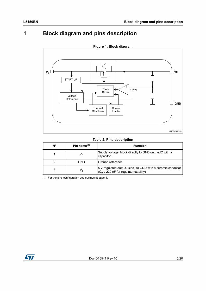
1 Block diagram and pins description
Figure 1. Block diagram
Table 2. Pins description
N° Pin name(1)
1. For the pins configuration see outlines at page 1.
Function
1 VSSupply voltage, block directly to GND on the IC with a capacitor.
2 GND Ground reference
3 Vo5 V regulated output. Block to GND with a ceramic capacitor (C0 ≥ 220 nF for regulator stability)
Electrical specifications L5150BN
6/20 DocID15541 Rev 10
2 Electrical specifications
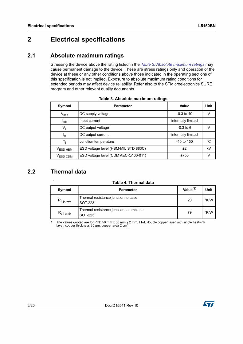
2.1 Absolute maximum ratingsStressing the device above the rating listed in the Table 3: Absolute maximum ratings may cause permanent damage to the device. These are stress ratings only and operation of the device at these or any other conditions above those indicated in the operating sections of this specification is not implied. Exposure to absolute maximum rating conditions for extended periods may affect device reliability. Refer also to the STMicroelectronics SURE program and other relevant quality documents.
2.2 Thermal data m
Table 3. Absolute maximum ratings
Symbol Parameter Value Unit
Vsdc DC supply voltage -0.3 to 40 V
Isdc Input current internally limited
Vo DC output voltage -0.3 to 6 V
Io DC output current internally limited
Tj Junction temperature -40 to 150 °C
VESD HBM ESD voltage level (HBM-MIL STD 883C) ±2 kV
VESD CDM ESD voltage level (CDM AEC-Q100-011) ±750 V
Table 4. Thermal data
Symbol Parameter Value(1)
1. The values quoted are for PCB 58 mm x 58 mm x 2 mm, FR4, double copper layer with single heatsink layer, copper thickness 35 μm, copper area 2 cm2.
Unit
Rthj-caseThermal resistance junction to case:SOT-223
20 °K/W
Rthj-ambThermal resistance junction to ambient:SOT-223
79 °K/W

DocID15541 Rev 10 7/20
L5150BN Electrical specifications
19
2.3 Electrical characteristicsValues specified in this section are for VS = 5.6 V to 31 V, Tj = -40 °C to +150 °C unless otherwise stated.
Table 5. General
Pin Symbol Parameter Test condition Min. Typ. Max. Unit
Vo Vo_ref Output voltage VS = 8 V to 18 V, Io = 8 mA to 150 mA 4.9 5.0 5.1 V
Vo Vo_ref Output voltage VS = 5.6 V to 31 V, Io = 8 mA to 150 mA 4.85 5.0 5.15 V
Vo Vo_ref Output voltage VS = 5.6 V to 31 V, Io = 0.1 mA to 8 mA 4.75 5.0 5.25 V
Vo Ishort Short-circuit current VS = 13.5 V 0.65 1.10 1.45 A
Vo Ilim Output current limitation(1) VS = 13.5 V 0.28 0.45 0.66 A
VS, Vo Vline Line regulation voltage VS = 6 V to 28 V, Io = 30 mA – – 40 mV
Vo Vload Load regulation voltage
VS = 8 V to 18 V, Io = 8 mA to 150 mA – – 55
mVVS = 13.5 V, Tj = 25 °C, Io = 8 mA to 150 mA
– – 40
VS, Vo Vdp Drop voltage(2) Io = 150 mA - - 500 mV
VS, Vo SVR Ripple rejection fr = 100 Hz(3) – 48 – dB
Vo Ioth_HNormal consumption mode output current VS = 8 V to 18 V 8 – – mA
Vo Ioth_LVery low consumption mode output current VS = 8 V to 18 V – – 1.1 mA
Vo Ioth_HystOutput current switching threshold hysteresis VS = 13.5 V, Tj = 25 °C – 0.8 – mA
VS, Vo Iqn_1 Current consumptionIqn_1 = IVs – Io
VS = 13.5 V,Io = 0.1 mA to 1 mA, Tj = 25 °C
– 50 80μA
VS = 13.5 V, Io = 0.1 mA to 1 mA, – 95
VS, Vo Iqn_150Current consumptionIqn_150 = IVs – Io
VS = 13.5 V, Io = 150 mA – 3.2 4.2 mA
– Tw Thermal protection temperature – 150 190 °C
– Tw_hyThermal protection temperature hysteresis – – 10 – °C
1. Measured output current when the output voltage has dropped 100 mV from its nominal value obtained at 13.5 V and Io = 75 mA.
2. VS - Vo measured dropout when the output voltage has dropped 100 mV from its nominal value obtained at 13.5 V and Io = 75 mA.
3. Guaranteed by design.

Electrical specifications L5150BN
8/20 DocID15541 Rev 10
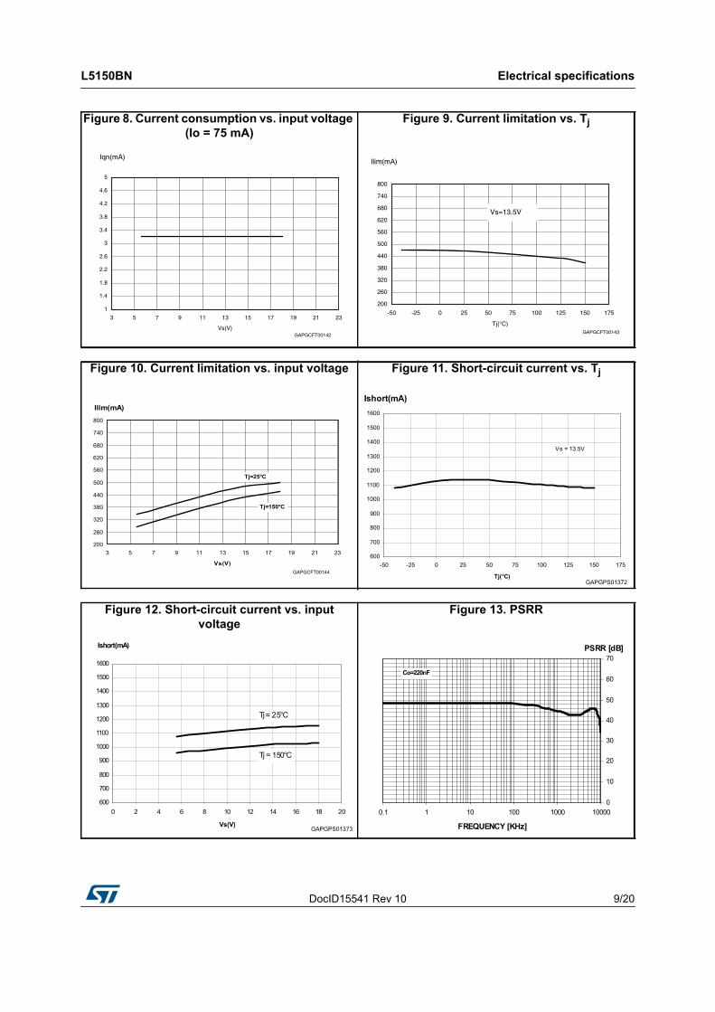
2.4 Electrical characteristics curves
Figure 2. Output voltage vs. Tj Figure 3. Output voltage vs. VS
Figure 4. Drop voltage vs. output current Figure 5. Current consumption vs. output current
Figure 6. Current consumption vs. output current (at light load condition)
Figure 7. Current consumption vs. input voltage (Io = 0.1 mA)
DocID15541 Rev 10 9/20
L5150BN Electrical specifications
19
Figure 8. Current consumption vs. input voltage (Io = 75 mA)
Figure 9. Current limitation vs. Tj
Figure 10. Current limitation vs. input voltage Figure 11. Short-circuit current vs. Tj
Figure 12. Short-circuit current vs. input voltage
Figure 13. PSRR
Electrical specifications L5150BN
10/20 DocID15541 Rev 10
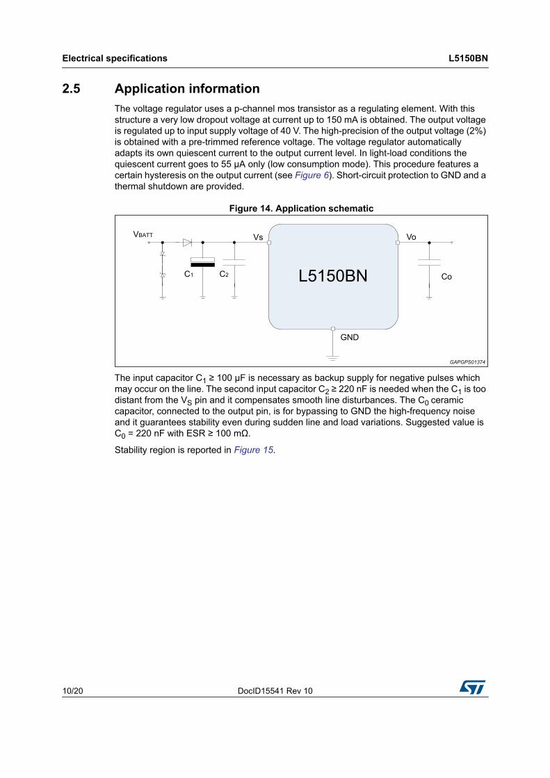
2.5 Application informationThe voltage regulator uses a p-channel mos transistor as a regulating element. With this structure a very low dropout voltage at current up to 150 mA is obtained. The output voltage is regulated up to input supply voltage of 40 V. The high-precision of the output voltage (2%) is obtained with a pre-trimmed reference voltage. The voltage regulator automatically adapts its own quiescent current to the output current level. In light-load conditions the quiescent current goes to 55 μA only (low consumption mode). This procedure features a certain hysteresis on the output current (see Figure 6). Short-circuit protection to GND and a thermal shutdown are provided.
Figure 14. Application schematic
The input capacitor C1 ≥ 100 μF is necessary as backup supply for negative pulses which may occur on the line. The second input capacitor C2 ≥ 220 nF is needed when the C1 is too distant from the VS pin and it compensates smooth line disturbances. The C0 ceramic capacitor, connected to the output pin, is for bypassing to GND the high-frequency noise and it guarantees stability even during sudden line and load variations. Suggested value is C0 = 220 nF with ESR ≥ 100 mΩ.
Stability region is reported in Figure 15.
DocID15541 Rev 10 11/20
L5150BN Electrical specifications
19
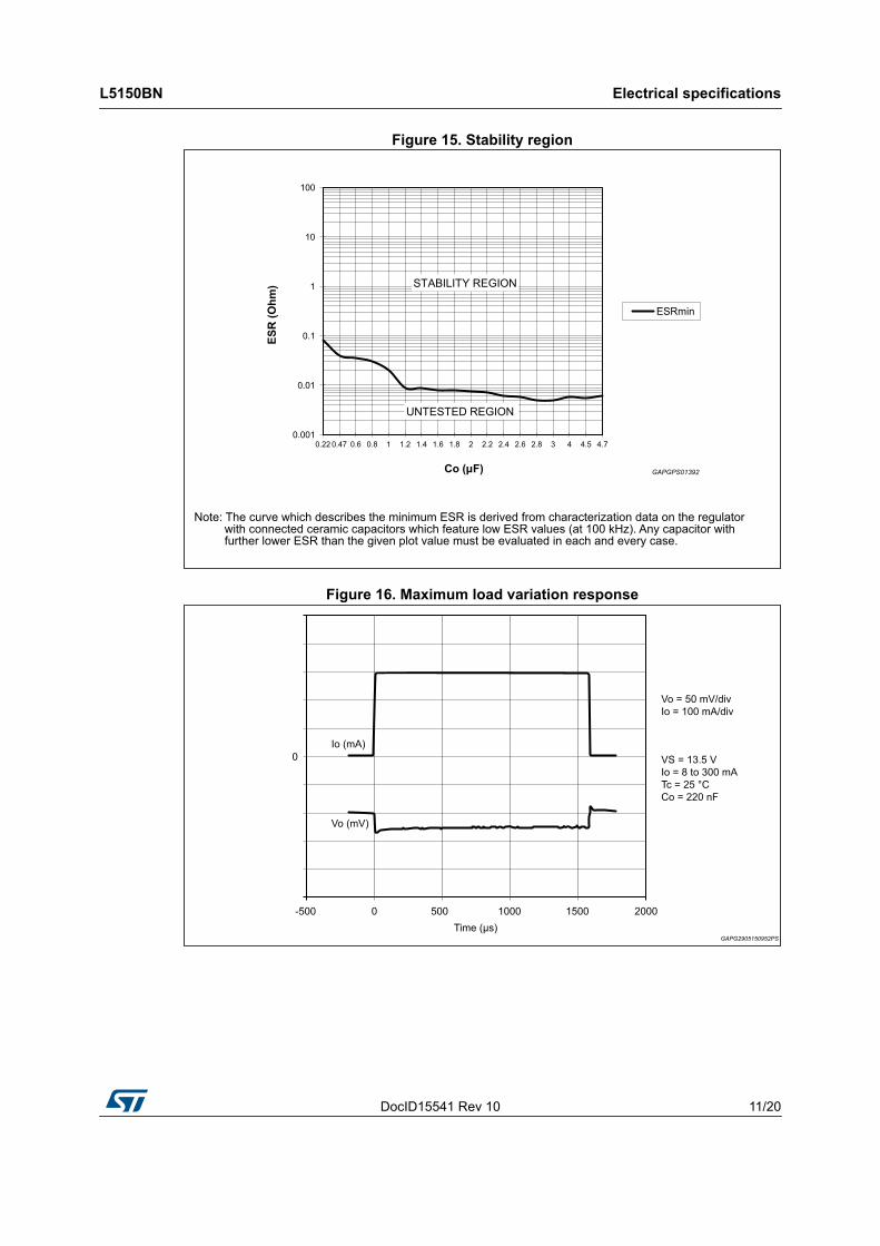
Figure 15. Stability region
Figure 16. Maximum load variation response
Note: The curve which describes the minimum ESR is derived from characterization data on the regulator with connected ceramic capacitors which feature low ESR values (at 100 kHz). Any capacitor with further lower ESR than the given plot value must be evaluated in each and every case.
Package and PCB thermal data L5150BN
12/20 DocID15541 Rev 10
3 Package and PCB thermal data
3.1 SOT-223 thermal data
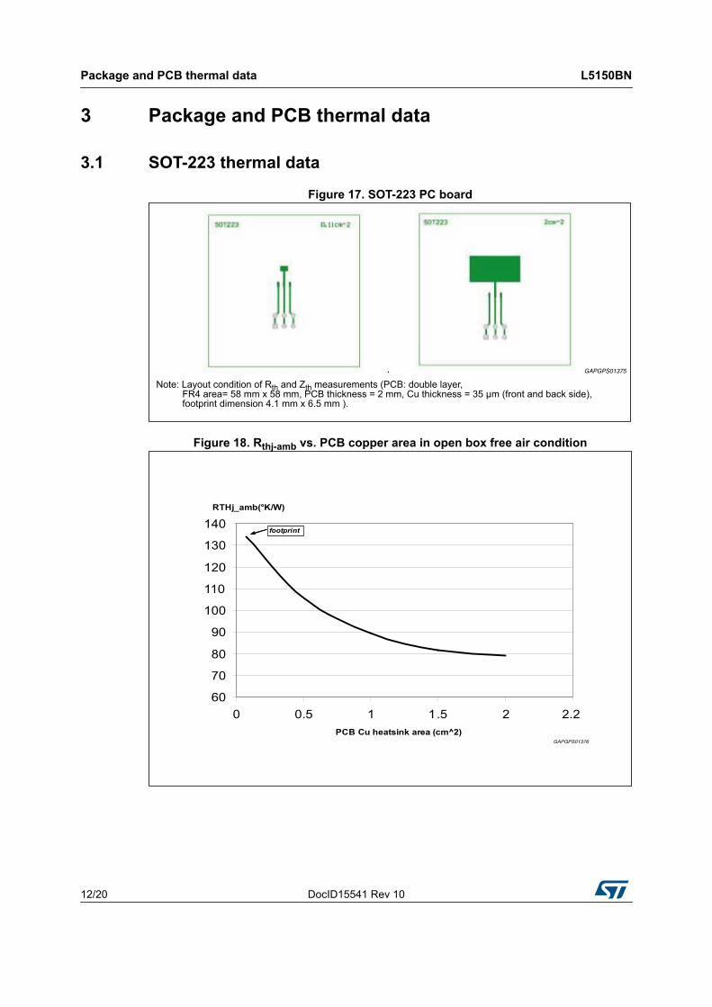
Figure 17. SOT-223 PC board
Figure 18. Rthj-amb vs. PCB copper area in open box free air condition
.
Note: Layout condition of Rth and Zth measurements (PCB: double layer, FR4 area= 58 mm x 58 mm, PCB thickness = 2 mm, Cu thickness = 35 μm (front and back side), footprint dimension 4.1 mm x 6.5 mm ).

ZTH RTH ZTHtp 1 – +=
DocID15541 Rev 10 13/20
L5150BN Package and PCB thermal data
19
Figure 19. SOT-223 thermal impedance junction ambient single pulse
Equation 1: pulse calculation formula
where = tP/T
Figure 20. Thermal fitting model of Vreg in SOT-223
Package and PCB thermal data L5150BN
14/20 DocID15541 Rev 10
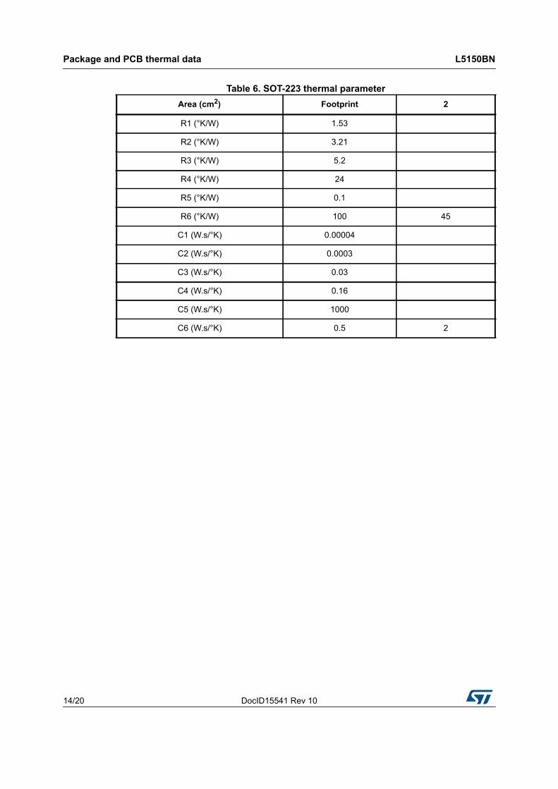
Table 6. SOT-223 thermal parameterArea (cm2) Footprint 2
R1 (°K/W) 1.53
R2 (°K/W) 3.21
R3 (°K/W) 5.2
R4 (°K/W) 24
R5 (°K/W) 0.1
R6 (°K/W) 100 45
C1 (W.s/°K) 0.00004
C2 (W.s/°K) 0.0003
C3 (W.s/°K) 0.03
C4 (W.s/°K) 0.16
C5 (W.s/°K) 1000
C6 (W.s/°K) 0.5 2

DocID15541 Rev 10 15/20
L5150BN Package information
19
4 Package information
In order to meet environmental requirements, ST offers these devices in different grades of ECOPACK® packages, depending on their level of environmental compliance. ECOPACK® specifications, grade definitions and product status are available at: www.st.com. ECOPACK® is an ST trademark.Package and packing information
4.1 SOT-223 package information
Figure 21. SOT-223 package outline
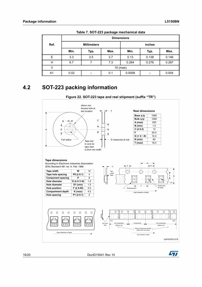
Table 7. SOT-223 package mechanical data
Ref.
Dimensions
Millimeters inches
Min. Typ. Max. Min. Typ. Max.
A – – 1.8 – – 0.071
B 0.6 0.7 0.85 0.024 0.027 0.033
B1 2.9 3 3.15 0.114 0.118 0.124
c 0.24 0.26 0.35 0.009 0.01 0.014
D 6.3 6.5 6.7 0.248 0.256 0.264
e – 2.3 – – 0.09 –
e1 – 4.6 – – 0.181 –
Package information L5150BN
16/20 DocID15541 Rev 10
4.2 SOT-223 packing informationFigure 22. SOT-223 tape and reel shipment (suffix “TR”)
E 3.3 3.5 3.7 0.13 0.138 0.146
H 6.7 7 7.3 0.264 0.276 0.287
V 10 (max)
A1 0.02 – 0.1 0.0008 – 0.004
Table 7. SOT-223 package mechanical data
Ref.
Dimensions
Millimeters inches
Min. Typ. Max. Min. Typ. Max.

DocID15541 Rev 10 17/20
L5150BN Revision history
19
5 Revision history
Table 8. Document revision history
Date Revision Changes
18-Jun-2007 1 Initial release.
14-May-2008 2
Corrected Table 2: Pins description : inverted 1 and 3 pins descriptions.Updated Table 5: General :– Vo_ref parameter: updated test conditions and values.– Vline and Vshort : updated test condition– Ishort: changed values from 0.65/0.95/1.25 to 0.65/1.10/1.45
(Min/Typ/Max)– Ilim: changed values from 0.7/1/1.30 to 0.28/0.45/0.66, added note– Vdp: added note– Inserted Ioth_L, Ioth_H, Ioth_Hyst rows– Iqn_1: changed values from 38/48 to 48/70 (Typ/Max).
09-Sep-2008 3Updated Table 5: General :– Vload parameter: changed test conditions.
Revision history L5150BN
18/20 DocID15541 Rev 10
16-Jun-2009 4
Updated corporate template (from V2 to V3)Changed document titleSection : Features on cover page– Iq on table: changed value from 48 μA to 50 μA– Added row in bullet listTable 2: Pins descriptionVo: changed ceramic capacitor expression for FunctionTable 3: Absolute maximum ratings– Updated all symbolsTable 4: Thermal data– Rthj-amb: changed value– Updated TableFootnoteTable 5: General– Vload: changed max value for Vs = 8 V to 18 V, added new row– Iqn_1: changed Test condition (added Tj = 25 °C), changed typ/max
value for Tj = 25 °C , added new row– Iqn_150: changed typ valueAdded Figure 2: Output voltage vs. TjAdded Figure 3: Output voltage vs. VSAdded Figure 4: Drop voltage vs. output currentAdded Figure 5: Current consumption vs. output currentAdded Figure 6: Current consumption vs. output current (at light load condition)Added Figure 7: Current consumption vs. input voltage (Io = 0.1 mA)Added Figure 8: Current consumption vs. input voltage (Io = 75 mA)Added Figure 9: Current limitation vs. TjAdded Figure 10: Current limitation vs. input voltageAdded Figure 11: Short-circuit current vs. TjAdded Figure 12: Short-circuit current vs. input voltageAdded Figure 13: PSRRSection 2.5: Application information– Changed section title from “Voltage regulator“ to “Application
information“– Updated text– Added Figure 14: Application schematic– Added Figure 16: Maximum load variation responseAdded Section 3: Package and PCB thermal dataChanged Section 4.1: ECOPACK®
04-Dec-2009 5Updated features list.Updated Section 2.5: Application information.
06-Apr-2010 6Updated Table 5: General:– Iqn_1 and Iqn_150: updated test parameter.
30-Jan-2012 7 Modified Figure 15: Stability region on page 11.
07-Feb-2012 8 Modified Figure 15: Stability region on page 11.
Table 8. Document revision history (continued)
Date Revision Changes
DocID15541 Rev 10 19/20
L5150BN Revision history
19
23-Sep-2013 9 Updated disclaimer.
03-Jun-2015 10 Changed in Table 5 the typical value of SVR from 60 dB to 48 dB.
Table 8. Document revision history (continued)
Date Revision Changes
L5150BN
20/20 DocID15541 Rev 10
IMPORTANT NOTICE – PLEASE READ CAREFULLY
STMicroelectronics NV and its subsidiaries (“ST”) reserve the right to make changes, corrections, enhancements, modifications, and improvements to ST products and/or to this document at any time without notice. Purchasers should obtain the latest relevant information on ST products before placing orders. ST products are sold pursuant to ST’s terms and conditions of sale in place at the time of order acknowledgement.
Purchasers are solely responsible for the choice, selection, and use of ST products and ST assumes no liability for application assistance or the design of Purchasers’ products.
No license, express or implied, to any intellectual property right is granted by ST herein.
Resale of ST products with provisions different from the information set forth herein shall void any warranty granted by ST for such product.
ST and the ST logo are trademarks of ST. All other product or service names are the property of their respective owners.
Information in this document supersedes and replaces information previously supplied in any prior versions of this document.
© 2015 STMicroelectronics – All rights reserved