40gbase-sr bi-directional qsfp+ lc duplex …40gbase-sr bi-directional qsfp+ lc duplex transceiver...
TRANSCRIPT

40GBASE-SR Bi-Directional QSFP+ LC Duplex Transceiver for MMF
1www.fs.com
QSFP-BD-40G
• 40 Gigabit Ethernet interconnects
• Datacom/Telecom switch & router connections
• Data aggregation and backplane applications
• Proprietary protocol and density applications
Application
Features
• Compliant to the 40GbE XLPPI electrical
specification per IEEE 802.3ba-2010
• Compliant to QSFP+ SFF-8436 Specification
• Aggregate bandwidth of > 40Gbps
• Operates at 10.3125 Gbps per electrical
channel with 64b/66b encoded data
• QSFP MSA compliant
• Capable of over 100m transmission on
OM3 Multimode Fiber (MMF)and 150m
on OM4 MMF
• Single +3.3V power supply operating
• Built-in digital diagnostic functions
• Temperature range 0°C to 70°C
• RoHS Compliant Part
• Utilizes a standard LC duplex fiber cable
allowing reuse of existing cable
infrastructure
40GBASE-SR BI-DIRECTIONAL QSFP+ LC DUPLEX TRANSCEIVER FOR MMF

Description
Products Specifications
2www.fs.com
It is a Four-Channel, Pluggable, LC Duplex, Fiber-Optic QSFP+ Transceiver for 40 Gigabit Ethernet Applications. This transceiver is a high
performance module for short-range duplex data communication and interconnect applications. It integrates four electrical data lanes in
each direction into transmission over a single LC duplex fiber optic cable. Each electrical lane operates at 10.3125 Gbps and conforms to
the 40GE XLPPI interface.
The transceiver internally multiplexes an XLPPI 4x10G interface into two 20Gb/s electrical channels, transmitting and receiving each
optically over one simplex LC fiber using bi-directional optics. This results in an aggregate bandwidth of 40Gbps into a duplex LC cable.
This allows reuse of the installed LC duplex cabling infrastructure for 40GbE application. Link distances up to 100 m using OM3 and
150m using OM4 optical fiber are supported. These modules are de- signed to operate over multimode fiber systems using a nominal
wavelength of 850nm on one end and 900nm on the other end. The electrical interface uses a 38 contact QSFP+ type edge connector.
The optical interface uses a conventional LC duplex connector.
I. Absolute Maximum Ratings
Data Rate Specifications Symbol Min Typ. Max Unit
Storage Temperature TS -40 +85 °C
Supply Voltage VCCT, R -0.5 4 V
Relative Humidity RH 0 85 %
40GBASE-SR BI-DIRECTIONAL QSFP+ LC DUPLEX TRANSCEIVER FOR MMF

3www.fs.com
40GBASE-SR BI-DIRECTIONAL QSFP+ LC DUPLEX TRANSCEIVER FOR MMF
Parameter Symbol Min Typ. Max Unit
Case operating Temperature TC 0 +70 °C
Supply Voltage VCCT, R +3.13 3.3 +3.47 V
Supply Current ICC 1000 mA
Power Dissipation PD 3.5 W
III. Electrical Characteristics (TOP= 0 to 70 °C, VCC = 3.15 to 3.45 Volts)
Parameter Symbol Min Typ. Max Unit Note
Data Rate per Channel 10.3125 11.2 Gbps
Power Consumption 2.5 3.5 W
Supply Current 0.75 1.0 A
Control I/O Voltage-High Icc Vcc V
Control I/O Voltage-Low VIH 2.0 0.7 V
Inter-Channel Skew VIL 0 150 Ps
RESETL Duration TSK 10 Us
RESETL De-assert time 100 ms
Power On Time 100 ms
II. Recommended Operating Environment

4www.fs.com
40GBASE-SR BI-DIRECTIONAL QSFP+ LC DUPLEX TRANSCEIVER FOR MMF
Transmitter
Single Ended Output Voltage Tolerance
0.3 4 V 1
Common mode Voltage Tolerance
15 mV
Transmit Input Diff Voltage VI 120 1200 mV
Transmit Input Diff Impedance ZIN 80 100 120
Data Dependent Input Jitter DDJ 0.1 UI
Data Input Total Jitter TJ 0.28 UI
Receiver
Single Ended Output Voltage Tolerance
0.3 4 V
Rx Output Diff Voltage Vo 600 800 mV
Rx Output Rise and Fall Voltage
Tr/Tf 35 ps
Total Jitter TJ 0.7 UI
Deterministic Jitter DJ 0.42 UI
Note:
1. 20~80%

5www.fs.com
Parameter Symbol Min Typ. Max Unit Ref.
Transmitter
Optical Wavelength CH1 λ 832 850 868 nm
Optical Wavelength CH2 λ 882 900 918 nm
RMS Spectral Width Pm 0.5 0.65 nm
Average Optical Power per Channel
Pavg -4 -2.5 +5.0 dBm
Laser Off Power Per Channel Poff -30 dBm
Optical Wavelength CH1 ER 3.5 dB
Relative Intensity Noise Rin -128 dB/HZ 1
Optical Return Loss Tolerance
12 dB
40GBASE-SR BI-DIRECTIONAL QSFP+ LC DUPLEX TRANSCEIVER FOR MMF
Receiver
Optical Center Wavelength CH1
λ 882 900 918 nm
Optical Center Wavelength CH2
λ 832 850 868 nm
Receiver Sensitivity per Channel
R -6 dBm
Maximum Input Power PMAX +0.5 dBm
Receiver Reflectance Rrx 30 -12 dB
LOS De-Assert LOSD -14 dBm
LOS Assert LOSA -30 dBm
LOS Hysteresis LOSH 0.5 dB
Note:
1. 12dB Reflection
IV. Optical Characteristics (TOP = 0 to 70 ℃, VCC = 3.1 to 3.47 Volts)

6www.fs.com
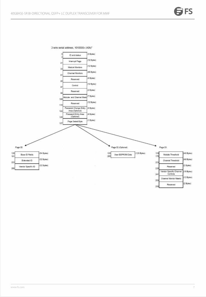
V. Diagnostic Monitoring Interface
40GBASE-SR BI-DIRECTIONAL QSFP+ LC DUPLEX TRANSCEIVER FOR MMF
Digital diagnostics monitoring function is available on all QSFP+ SRBD. A 2-wire serial interface provides user to contact with module.
The structure of the memory is shown in flowing. The memory space is arranged into a lower, single page, address space of 128 bytes
and multiple upper address space pages. This structure permits timely access to addresses in the lower page, such as Interrupt Flags and
Monitors. Less time critical time entries, such as serial ID information and threshold settings, are available with the Page Select function.
The interface address used is A0xh and is mainly used for time critical data like interrupt handling in order to enable a one-time-read for
all data related to an interrupt situation. After an interrupt, IntL, has been asserted, the host can read out the flag field to determine the
affected channel and type of flag.
Byte Address Description Type
0 Identifier(1 Byte) Read Only
1-2 Status (2 Bytes) Read Only
3-21 Interrupt Flags (31 Bytes) Read Only
22-33 Module Monitors (12 Bytes) Read Only
34-81 Channel Monitors (48 Bytes) Read Only
82-85 Reserved (4 Bytes) Read /Write
86-97 Control (12 Bytes) Read /Write
98-99 Reserved (2 Bytes) Read /Write
100-106 Module and Channel Masks ( 7 Bytes) Read /Write
107-118 Reserved (12 Bytes) Read /Write
119-122 Reserved (4 Bytes) Read /Write
123-126 Reserved ( 4 Bytes) Read /Write
127 Page Select Byte Read /Write
128-175 Module Thresholds (48 Bytes) Read Only
176-223 Reserved (48 Bytes) Read Only
224-225 Reserved (2 Bytes) Read /Write
226-239 Reserved (14 Bytes) Read /Write
240-241 Channel Controls (2 Bytes) Read /Write
242-253 Reserved (12 Bytes) Read /Write
254-255 Reserved (2 Bytes) Read /Write
7www.fs.com
40GBASE-SR BI-DIRECTIONAL QSFP+ LC DUPLEX TRANSCEIVER FOR MMF
8www.fs.com
40GBASE-SR BI-DIRECTIONAL QSFP+ LC DUPLEX TRANSCEIVER FOR MMF
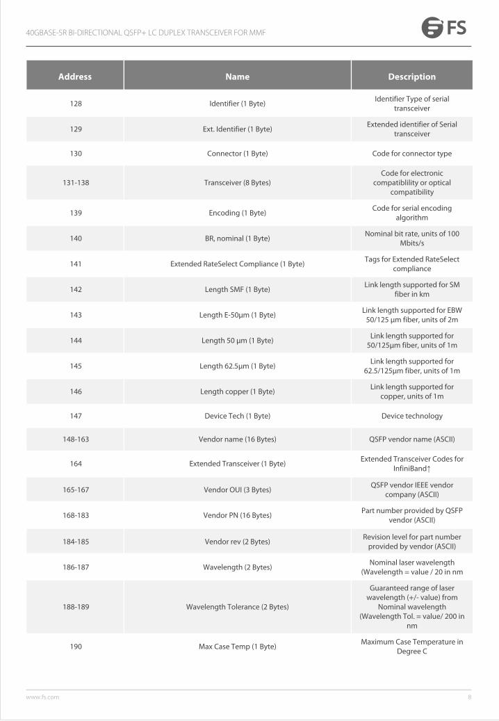
Address Name Description
128 Identifier (1 Byte)Identifier Type of serial
transceiver
129 Ext. Identifier (1 Byte)Extended identifier of Serial
transceiver
130 Connector (1 Byte) Code for connector type
131-138 Transceiver (8 Bytes)Code for electronic
compatiblility or optical compatibility
139 Encoding (1 Byte)Code for serial encoding
algorithm
140 BR, nominal (1 Byte)Nominal bit rate, units of 100
Mbits/s
141 Extended RateSelect Compliance (1 Byte)Tags for Extended RateSelect
compliance
142 Length SMF (1 Byte)Link length supported for SM
fiber in km
143 Length E-50μm (1 Byte)Link length supported for EBW
50/125 μm fiber, units of 2m
144 Length 50 μm (1 Byte)Link length supported for
50/125μm fiber, units of 1m
145 Length 62.5μm (1 Byte)Link length supported for
62.5/125μm fiber, units of 1m
146 Length copper (1 Byte)Link length supported for
copper, units of 1m
147 Device Tech (1 Byte) Device technology
148-163 Vendor name (16 Bytes) QSFP vendor name (ASCII)
164 Extended Transceiver (1 Byte)Extended Transceiver Codes for
InfiniBand↑
165-167 Vendor OUI (3 Bytes)QSFP vendor IEEE vendor
company (ASCII)
168-183 Vendor PN (16 Bytes)Part number provided by QSFP
vendor (ASCII)
184-185 Vendor rev (2 Bytes)Revision level for part number
provided by vendor (ASCII)
186-187 Wavelength (2 Bytes)Nominal laser wavelength
(Wavelength = value / 20 in nm
188-189 Wavelength Tolerance (2 Bytes)
Guaranteed range of laser wavelength (+/- value) from
Nominal wavelength (Wavelength Tol. = value/ 200 in
nm
190 Max Case Temp (1 Byte)Maximum Case Temperature in
Degree C

9www.fs.com
40GBASE-SR BI-DIRECTIONAL QSFP+ LC DUPLEX TRANSCEIVER FOR MMF
Address Name Description
191 CC-BASE (1 Byte)Check code for Base ID fields
(addresses 128-190)
192-195 Options (4 Bytes)Rate Select, TX Disable, TX Fault,
LOS
196-211 Vendor SN (16 Bytes)Serial number provided by
vendor (ASCII)
212-219 Date code (8 Bytes)Vendor's manufacturing date
code
220 Diagnostic Monitoring Type (1Byte)Indicates which type of
diagnostic monitoring is implemented
221 Enhanced Options (1Byte)Indicates which optional
enhanced features are implemented
222 Reserved (1Byte) Reserved
223 CC-EXTCheck code for the Extended ID
Fields ( addresses 192-222)
224-255 Vendor Specific (32 Bytes) Vendor Specific EEPROM
Page02 is User EEPROM and its format decided by user.
The detail description of low memory and page00.page03 upper memory please see SFF-8436 document.

VI. Timing for Soft Control and Status Functions
10www.fs.com
40GBASE-SR BI-DIRECTIONAL QSFP+ LC DUPLEX TRANSCEIVER FOR MMF
Parameter Symbol Max Unit Conditions
Initialization Time t_init 2000 msTime from power on1, hot plug or rising edge of
Reset until the module is fully functional2
Reset Init Assert Time t_reset_init 2 μsA Reset is generated by a low level longer than the minimum reset pulse time present on the
ResetL pin.
Serial Bus Hardware Ready Time
t_serial 2000 msTime from power on1 until module responds to
data transmission over the 2-wire serial bus
Monitor Data ReadyTime
t_data 2000 msTime from power on1 to data not ready, bit 0 of
Byte 2, deasserted and IntL asserted
Reset Assert Time t_reset 2000 msTime from rising edge on the ResetL pin until the
module is fully functional2
LPMode Assert Time ton_LPMode 100 μsTime from assertion of LPMode (Vin:LPMode =Vih)
until module power consumption enters lower Power Level
IntL Assert Time ton_IntL 200 msTime from occurrence of condition triggering IntL
until Vout:IntL = Vol
IntL Deassert Time toff_IntL 500 μs
toff_IntL 500 μs Time from clear on read3 operation of associated flag until Vout:IntL = Voh. This includes deassert times for Rx LOS, Tx Fault
and other flag bits.
Rx LOS Assert Time ton_los 100 ms
Time from Rx LOS state to Rx LOS bit set and IntL asserted
Flag Assert Time ton_flag 200 msTime from occurrence of condition triggering flag
to associated flag bit set and IntL asserted
Mask Assert Time ton_mask 100 msTime from mask bit set4 until associated IntL
assertion is inhibited
Mask De-assert Time toff_mask 100 msTime from mask bit cleared4 until associated IntlL
operation resumes

VI. Timing for Soft Control and Status Functions
11www.fs.com
40GBASE-SR BI-DIRECTIONAL QSFP+ LC DUPLEX TRANSCEIVER FOR MMF
Parameter Symbol Max Unit Conditions
ModSelL Assert Time ton_ModSelL 100 μsTime from assertion of ModSelL until module responds to data transmission over the 2-wire
serial bus
ModSelL Deassert Time toff_ModSelL 100 μsTime from deassertion of ModSelL until the
module does not respond to data transmission over the 2-wire serial bus
Power_over-ride or Power-set Assert Time
ton_Pdown 100 msTime from P_Down bit set 4 until module power
consumption enters lower Power Level
Power_over-ride or Power-set De-assert
Timetoff_Pdown 300 ms
Time from P_Down bit cleared4 until the module is fully functional3
Notes:
1. Power on is defined as the instant when supply voltages reach and remain at or above the minimum specified value.
2. Fully functional is defined as IntL asserted due to data not ready bit, bit 0 byte 2 de-asserted.
3. Measured from falling clock edge after stop bit of read transaction.
4. Measured from falling clock edge after stop bit of write transaction.

12www.fs.com
40GBASE-SR BI-DIRECTIONAL QSFP+ LC DUPLEX TRANSCEIVER FOR MMF
Diagram of Host Board Connector Block Pin Numbers and Name
Pin Logic Symbol Name/Description Ref.
1 GND Ground 1
2 CML-I Tx2n Transmitter Inverted Data Input
3 CML-I Tx2p Transmitter Non-Inverted Data output
4 GND Ground 1
5 CML-I Tx4n Transmitter Inverted Data Output
6 CML-I Tx4p Transmitter Non-Inverted Data Output
7 GND Ground 1
8 LVTTL-I ModSelL Module Select
9 LVTTL-I ResetL Module Reset
10 VccRx +3.3V Power Supply Receiver 2
VII. Pin Description

13www.fs.com
40GBASE-SR BI-DIRECTIONAL QSFP+ LC DUPLEX TRANSCEIVER FOR MMF
Pin Logic Symbol Name/Description Ref.
11 LVCMOS-I/O SCL 2-Wire Serial Interface Clock
12 LVCMOS-I/O SDA 2-Wire Serial Interface Data
13 GND Ground 1
14 CML-O Rx3p Receiver Inverted Data Output
15 CML-O Rx3n Receiver Non-Inverted Data Output
16 GND Ground 1
17 CML-O Rx1p Receiver Inverted Data Output
18 CML-O Rx1n Receiver Non-Inverted Data Output
19 GND Ground 1
20 GND Ground 1
21 CML-O Rx2n Receiver Inverted Data Output
22 CML-O Rx2p Receiver Non-Inverted Data Output
23 GND Ground 1
24 CML-O Rx4n Receiver Inverted Data Output
25 CML-O Rx4p Receiver Non-Inverted Data Output
26 GND Ground 1
27 LVTTL-O ModPrsL Module Present
28 LVTTL-O IntL Interrupt
29 VccTx +3.3V Power Supply Transmitter 2
30 Vcc1 +3.3V Power Supply 2
31 LVTTL-I LPMode Low Power Mode
32 GND Ground 1
33 CML-I Tx3p Transmitter Inverted Data Output

14www.fs.com
40GBASE-SR BI-DIRECTIONAL QSFP+ LC DUPLEX TRANSCEIVER FOR MMF
Pin Logic Symbol Name/Description Ref.
34 CML-I Tx3n Transmitter Non-Inverted Data Output
35 GND Ground 1
36 CML-I Tx1p Transmitter Inverted Data Output
37 CML-I Tx1n Transmitter Non-Inverted Data Output
38 GND Ground 1
Notes:
1. GND is the symbol for single and supply(power) common for QSFP modules, All are common within the QSFP module and all
module voltages are referenced to this potential otherwise noted. Connect these directly to the host board signal common
ground plane. Laser output disabled on TDIS >2.0V or open, enabled on TDIS <0.8V.
2. VccRx, Vcc1 and VccTx are the receiver and transmitter power suppliers and shall be applied concurrently. Recommended host
board power supply filtering is shown below. VccRx, Vcc1 and VccTx may be internally connected within the QSFP transceiver
module in any combination. The connector pins are each rated for maximum current of 500mA.

15www.fs.com
VIII.Recommended Circuit
40GBASE-SR BI-DIRECTIONAL QSFP+ LC DUPLEX TRANSCEIVER FOR MMF
IX. Mechanical Dimensions

16www.fs.com
Test Center
FS.COM transceivers are tested to ensure connectivity and compatibility in our test center before shipped out. FS.COM test center is
supported by a variety of mainstream original brand switches and groups of professional staff, helping our customers make the most
efficient use of our products in their systems, network designs and deployments.
The original switches could be found nowhere but at FS.COM test center, eg: Juniper MX960 & EX 4300 series, Cisco Nexus 9396PX &
Cisco ASR 9000 Series, HP 5900 Series & HP 5406R ZL2 V3(J9996A), Arista 7050S-64, Brocade ICX7750-26Q & ICX6610-48, Avaya VSP 7000
MDA 2, etc.
Cisco ASR 9000 Series(A9K-MPA-1X40GE) ARISTA 7050S-64(DCS-7050S-64) Juniper MX960
Brocade ICX 7750-26Q Extreme Networks X670V VIM-40G4X Mellanox M3601Q
Dell N4032F HP 5406R ZL2 V3(J9996A) AVAYA 7024XLS(7002QQ-MDA)
40GBASE-SR BI-DIRECTIONAL QSFP+ LC DUPLEX TRANSCEIVER FOR MMF

17www.fs.com
Test Assured Program
FS.COM truly understands the value of compatibility and interoperability to each optics. Every module FS.COM provides must run
through programming and an extensive series of platform diagnostic tests to prove its performance and compatibility. In our test center,
we care of every detail from staff to facilities—professionally trained staff, advanced test facilities and comprehensive original-brand
switches, to ensure our customers to receive the optics with superior quality.
Our smart data system allows effective product management and
quality control according to the unique serial number, properly
tracking the order, shipment and every part.
Our in-house coding facility programs all of our parts to standard
OEM specs for compatibility on all major vendors and systems such
as Cisco, Juniper, Brocade, HP, Dell, Arista and so on.
With a comprehensive line of original-brand switches, we can
recreate an environment and test each optics in practical
application to ensure quality and distance.
The last test assured step to ensure our products to be shipped
with perfect package.
40GBASE-SR BI-DIRECTIONAL QSFP+ LC DUPLEX TRANSCEIVER FOR MMF

18www.fs.com
Order Information
Part Number Description
QSFP-SR4-40G 40GBASE-SR4 QSFP+ 850nm 150m MTP/MPO Transceiver for MMF
QSFP-CSR4-40G 40GBASE-CSR4 QSFP+ 850nm 400m MTP/MPO Transceiver for MMF
QSFP-PIR4-40G 40GBASE-PLRL4 QSFP+ 1310nm 1.4km MTP/MPO Transceiver for SMF
QSFP-LX4-40G 40GBASE-UNIV QSFP+ 1310nm 2km LC Transceiver for SMF&MMF
QSFP-IR4-40G 40GBASE-LR4L QSFP+ 1310nm 2km LC Transceiver for SMF
QSFP-LR4-40G 40GBASE-LR4 and OTU3 QSFP+ 1310nm 10km LC Transceiver for SMF
QSFP-PLR4-40G 40GBASE-PLR4 QSFP+ 1310nm 10km MTP/MPO Transceiver for SMF
QSFP-ER4-40G 40GBASE-ER4 and OTU3 QSFP+ 1310nm 40km LC Transceiver for SMF
QSFP-BD-40G 40GBASE-SR Bi-Directional QSFP LC Duplex Transceiver for MMF
Notes:
1.40G QSFP+ transceiver module is individually tested on corresponding equipment such as Cisco, Arista, Juniper, Dell, Brocade and
other brands, and passes the monitoring of FS.COM intelligent quality control system.
40GBASE-SR BI-DIRECTIONAL QSFP+ LC DUPLEX TRANSCEIVER FOR MMF
