40a integrated ir3553 - hardware secrets · 40a integrated powirstage ... refer to international...
TRANSCRIPT

November 29, 2012 | FINAL DATASHEET1
IR355340A Integrated PowIRstage®
FEATURES
Peak efficiency up to 93.2% at 1.2V
Integrated driver, control MOSFET, synchronous MOSFET and Schottky diode
Input voltage (VIN) operating range up to 15V
Output voltage range from 0.25V up to 3.3V
Output current capability of 40A DC
Operation up to 1.0MHz
Integrated current sense amplifier
VCC under voltage lockout
Thermal flag
Body‐Braking® load transient support
Diode‐emulation high efficiency mode
Compatible with 3.3V PWM logic and VCC tolerant
Compliant with Intel DrMOS V4.0
PCB footprint compatible with IR3550 and IR3551
Efficient dual sided cooling
Small 4mm x 6mm x 0.9mm PQFN package
Lead free RoHS compliant package
APPLICATIONS
Voltage Regulators for CPUs, GPUs, and DDR memory arrays
High current, low profile DC‐DC converters
BASIC APPLICATION
SW
PWM
VIN
PGND
VCCVCC
BOOST
VIN
VOUT
PWM
CSIN+
CSIN‐
4.5V to 7V
LGND
IOUT IOUT
BBRK# BBRK#
REFIN REFIN
4.5V to 15V
IR3553
PHSFLT# PHSFLT#
Figure 1: IR3553 Basic Application Circuit
DESCRIPTION
The IR3553 integrated PowIRstage® is a synchronous buck gate driver co‐packed with a control MOSFET and a synchronous MOSFET with integrated Schottky diode. It is optimized internally for PCB layout, heat transfer and driver/MOSFET timing. Custom designed gate driver and MOSFET combination enables higher efficiency at lower output voltages required by cutting edge CPU, GPU and DDR memory designs.
Up to 1.0MHz switching frequency enables high performance transient response, allowing miniaturization of output inductors, as well as input and output capacitors while maintaining industry leading efficiency. The IR3553’s superior efficiency enables smallest size and lower solution cost. The IR3553 PCB footprint is compatible with the IR3550 (60A) and the IR3551 (50A).
Integrated current sense amplifier achieves superior current sense accuracy and signal to noise ratio vs. best‐in‐class controller based Inductor DCR sense methods.
The IR3553 incorporates the Body‐ Braking® feature which enables reduction of output capacitors. Synchronous diode emulation mode in the IR3553 removes the zero‐current detection burden from the PWM controller and increases system light‐load efficiency.
The IR3553 is optimized specifically for CPU core power delivery in server applications. The ability to meet the stringent requirements of the server market also makes the IR3553 ideally suited to powering GPU and DDR memory designs and other high current applications.
Figure 2: Typical IR3553 Efficiency & Power Loss (See Note 2 on Page 8)
74
76
78
80
82
84
86
88
90
92
94
0 5 10 15 20 25 30 35 40
Output Current (A)
Efficien
cy (%)
0
2
4
6
8
10
12
14
16
18
20Power Loss (W)
November 29, 2012 | FINAL DATASHEET2
IR355340A Integrated PowIRstage®
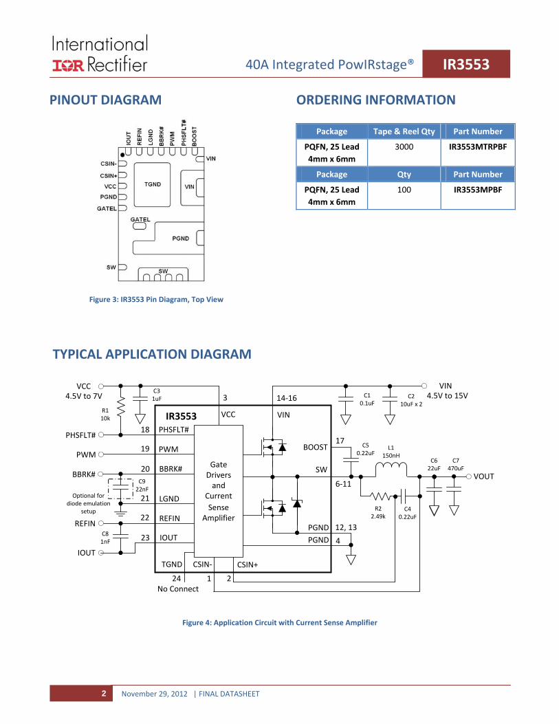
PINOUT DIAGRAM
Figure 3: IR3553 Pin Diagram, Top View
ORDERING INFORMATION
Package Tape & Reel Qty Part Number
PQFN, 25 Lead
4mm x 6mm
3000 IR3553MTRPBF
Package Qty Part Number
PQFN, 25 Lead
4mm x 6mm
100 IR3553MPBF
TYPICAL APPLICATION DIAGRAM
SW
PWM
VIN
PGND
Gate Drivers and
Current
Sense Amplifier
LGND
VCC
PHSFLT#
IOUT
VCC
BOOST
VIN
PWM
IOUT
PHSFLT#
BBRK#BBRK#
REFINREFIN
CSIN‐ CSIN+
IR3553
4.5V to 7V 4.5V to 15VC210uF x 2
C50.22uF
C31uF
R110k
C40.22uF
R22.49k
L1150nH
3 14‐16
17
18
19
20
22
21
23
1 2
12, 13
6‐11
C10.1uF
PGND 4
24
TGND
No Connect
C81nF
C922nF
Optional for diode emulation
setup
VOUT
C7470uF
C622uF
Figure 4: Application Circuit with Current Sense Amplifier

November 29, 2012 | FINAL DATASHEET3
IR355340A Integrated PowIRstage®
TYPICAL APPLICATION DIAGRAM (CONTINUED)
SW
PWM
VIN
PGND
Gate Drivers and
Current
Sense Amplifier
IOUT
VCC
PHSFLT#
VCC
BOOST
VIN
PWM
REFIN
PHSFLT#
BBRK#BBRK#
CS+
LGND
CSIN‐ CSIN+
IR3553
4.5V to 7V 4.5V to 15VC210uF x 2
C50.22uF
C30.1uF
R110k
C40.22uF
R22.49k
L1150nH
3 14‐16
17
18
19
20
21
23
22
1 2
12, 13
6‐11
C10.1uF
PGND 4
24
TGND
No Connect
CS‐
VOUT
C7470uF
C622uF
Figure 5: Application Circuit without Current Sense Amplifier
FUNCTIONAL BLOCK DIAGRAM
PWM
6
7
8
9
10
11
14 15 16
VIN VIN VIN
SW
SW
SW
SW
SW
SW
1 4 12 13
CSIN‐ PGNDPGNDPGND
17
BOOST
Power‐on Reset (POR),
3.3V Reference,
and
Dead‐time Control
19
IOUT 23
VCC 3
BBRK# 20
255
GATEL GATEL
Driver
Driver18PHSFLT#
2
CSIN+
21LGND
22REFIN
Current Sense Amplifier
MOSFET
& Thermal Detection
S Q
R
POR
3.3V VCC
‐+
3.3V
24
TGND
Figure 6: IR3553 Functional Block Diagram
November 29, 2012 | FINAL DATASHEET4
IR355340A Integrated PowIRstage®
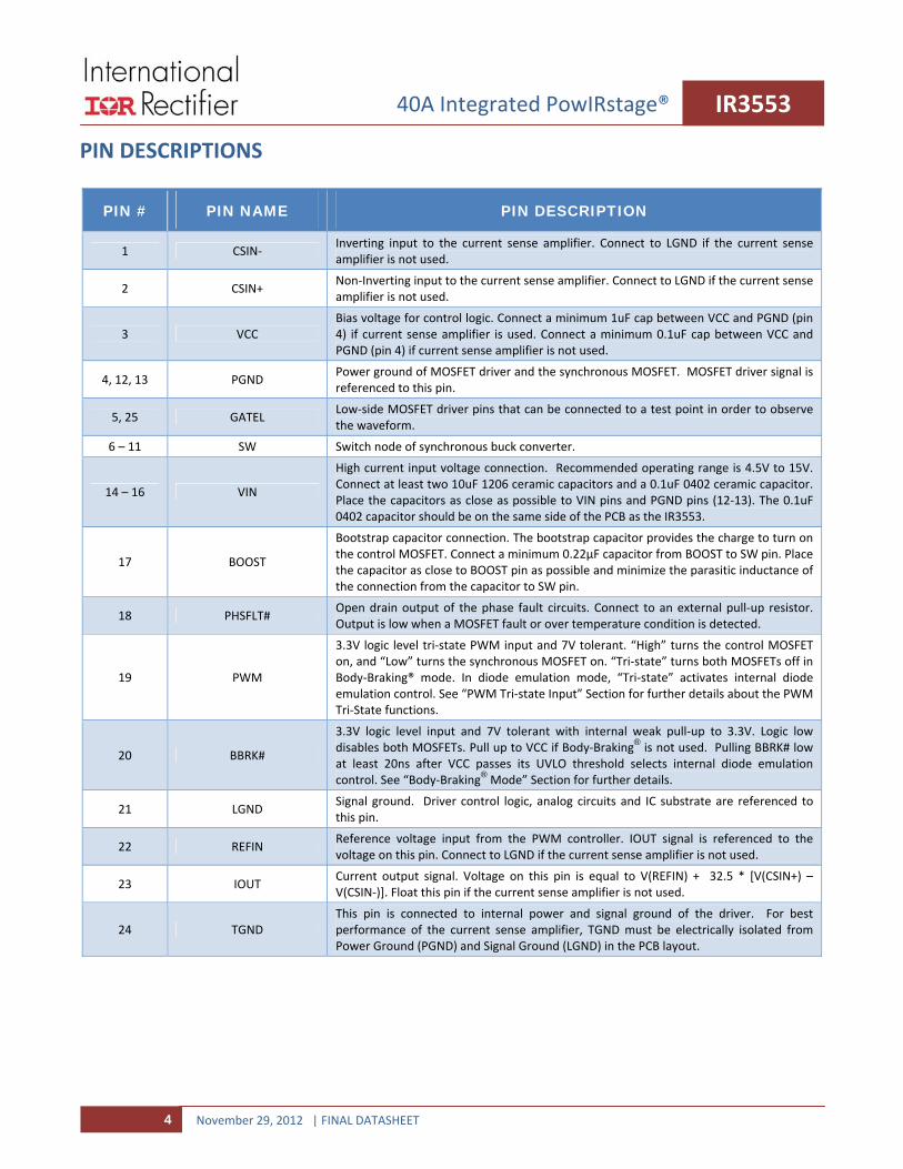
PIN DESCRIPTIONS
PIN # PIN NAME PIN DESCRIPTION
1 CSIN‐ Inverting input to the current sense amplifier. Connect to LGND if the current sense amplifier is not used.
2 CSIN+ Non‐Inverting input to the current sense amplifier. Connect to LGND if the current sense amplifier is not used.
3 VCC Bias voltage for control logic. Connect a minimum 1uF cap between VCC and PGND (pin 4) if current sense amplifier is used. Connect a minimum 0.1uF cap between VCC and PGND (pin 4) if current sense amplifier is not used.
4, 12, 13 PGND Power ground of MOSFET driver and the synchronous MOSFET. MOSFET driver signal is referenced to this pin.
5, 25 GATEL Low‐side MOSFET driver pins that can be connected to a test point in order to observe the waveform.
6 – 11 SW Switch node of synchronous buck converter.
14 – 16 VIN
High current input voltage connection. Recommended operating range is 4.5V to 15V. Connect at least two 10uF 1206 ceramic capacitors and a 0.1uF 0402 ceramic capacitor. Place the capacitors as close as possible to VIN pins and PGND pins (12‐13). The 0.1uF 0402 capacitor should be on the same side of the PCB as the IR3553.
17 BOOST
Bootstrap capacitor connection. The bootstrap capacitor provides the charge to turn on the control MOSFET. Connect a minimum 0.22µF capacitor from BOOST to SW pin. Place the capacitor as close to BOOST pin as possible and minimize the parasitic inductance of the connection from the capacitor to SW pin.
18 PHSFLT# Open drain output of the phase fault circuits. Connect to an external pull‐up resistor. Output is low when a MOSFET fault or over temperature condition is detected.
19 PWM
3.3V logic level tri‐state PWM input and 7V tolerant. “High” turns the control MOSFET on, and “Low” turns the synchronous MOSFET on. “Tri‐state” turns both MOSFETs off in Body‐Braking® mode. In diode emulation mode, “Tri‐state” activates internal diode emulation control. See “PWM Tri‐state Input” Section for further details about the PWM Tri‐State functions.
20 BBRK#
3.3V logic level input and 7V tolerant with internal weak pull‐up to 3.3V. Logic low disables both MOSFETs. Pull up to VCC if Body‐Braking® is not used. Pulling BBRK# low at least 20ns after VCC passes its UVLO threshold selects internal diode emulation control. See “Body‐Braking® Mode” Section for further details.
21 LGND Signal ground. Driver control logic, analog circuits and IC substrate are referenced to this pin.
22 REFIN Reference voltage input from the PWM controller. IOUT signal is referenced to the voltage on this pin. Connect to LGND if the current sense amplifier is not used.
23 IOUT Current output signal. Voltage on this pin is equal to V(REFIN) + 32.5 * [V(CSIN+) – V(CSIN‐)]. Float this pin if the current sense amplifier is not used.
24 TGND This pin is connected to internal power and signal ground of the driver. For best performance of the current sense amplifier, TGND must be electrically isolated from Power Ground (PGND) and Signal Ground (LGND) in the PCB layout.
November 29, 2012 | FINAL DATASHEET5
IR355340A Integrated PowIRstage®
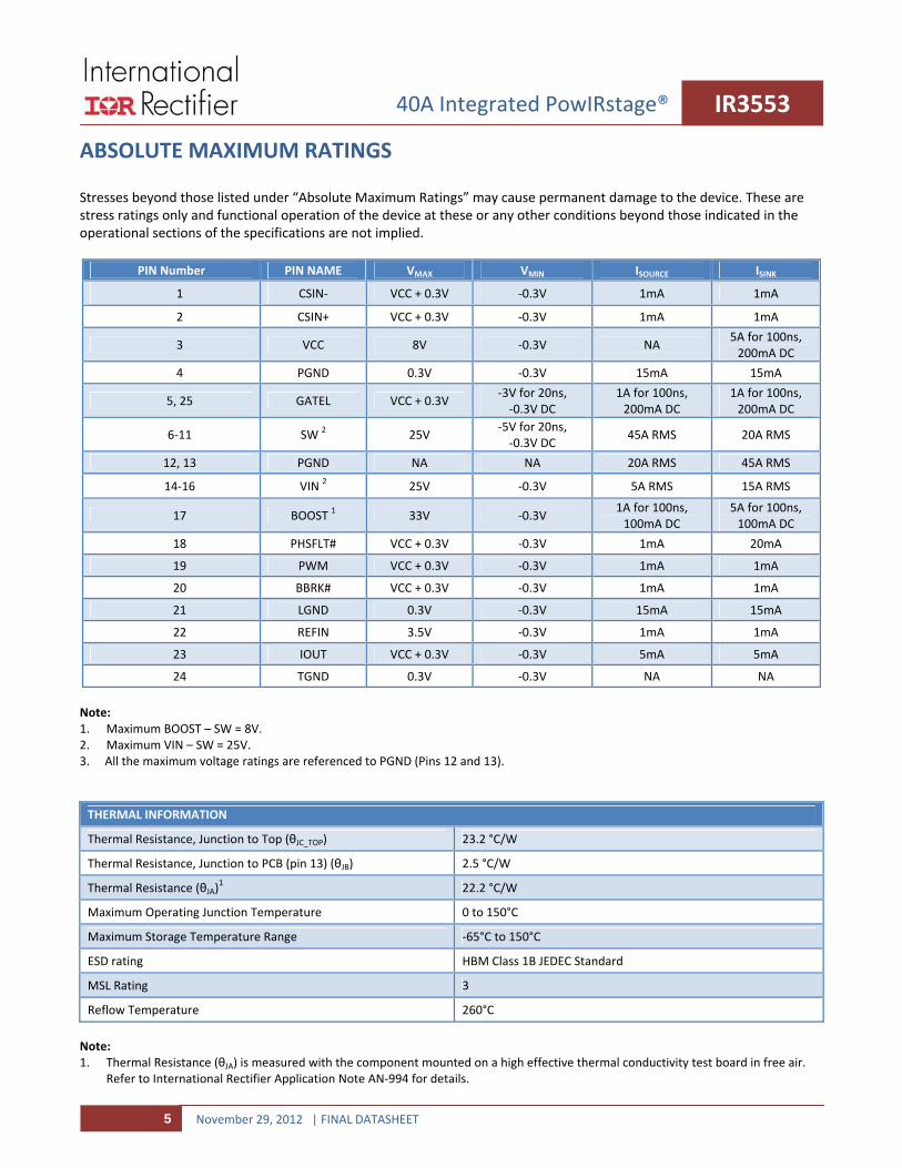
ABSOLUTE MAXIMUM RATINGS
Stresses beyond those listed under “Absolute Maximum Ratings” may cause permanent damage to the device. These are stress ratings only and functional operation of the device at these or any other conditions beyond those indicated in the operational sections of the specifications are not implied.
PIN Number PIN NAME VMAX VMIN ISOURCE ISINK
1 CSIN‐ VCC + 0.3V ‐0.3V 1mA 1mA
2 CSIN+ VCC + 0.3V ‐0.3V 1mA 1mA
3 VCC 8V ‐0.3V NA 5A for 100ns, 200mA DC
4 PGND 0.3V ‐0.3V 15mA 15mA
5, 25 GATEL VCC + 0.3V ‐3V for 20ns, ‐0.3V DC
1A for 100ns, 200mA DC
1A for 100ns, 200mA DC
6‐11 SW 2 25V ‐5V for 20ns, ‐0.3V DC
45A RMS 20A RMS
12, 13 PGND NA NA 20A RMS 45A RMS
14‐16 VIN 2 25V ‐0.3V 5A RMS 15A RMS
17 BOOST 1 33V ‐0.3V 1A for 100ns, 100mA DC
5A for 100ns, 100mA DC
18 PHSFLT# VCC + 0.3V ‐0.3V 1mA 20mA
19 PWM VCC + 0.3V ‐0.3V 1mA 1mA
20 BBRK# VCC + 0.3V ‐0.3V 1mA 1mA
21 LGND 0.3V ‐0.3V 15mA 15mA
22 REFIN 3.5V ‐0.3V 1mA 1mA
23 IOUT VCC + 0.3V ‐0.3V 5mA 5mA
24 TGND 0.3V ‐0.3V NA NA
Note: 1. Maximum BOOST – SW = 8V. 2. Maximum VIN – SW = 25V. 3. All the maximum voltage ratings are referenced to PGND (Pins 12 and 13).
THERMAL INFORMATION
Thermal Resistance, Junction to Top (θJC_TOP) 23.2 °C/W
Thermal Resistance, Junction to PCB (pin 13) (θJB) 2.5 °C/W
Thermal Resistance (θJA)1 22.2 °C/W
Maximum Operating Junction Temperature 0 to 150°C
Maximum Storage Temperature Range ‐65°C to 150°C
ESD rating HBM Class 1B JEDEC Standard
MSL Rating 3
Reflow Temperature 260°C
Note: 1. Thermal Resistance (θJA) is measured with the component mounted on a high effective thermal conductivity test board in free air.
Refer to International Rectifier Application Note AN‐994 for details.
November 29, 2012 | FINAL DATASHEET6
IR355340A Integrated PowIRstage®
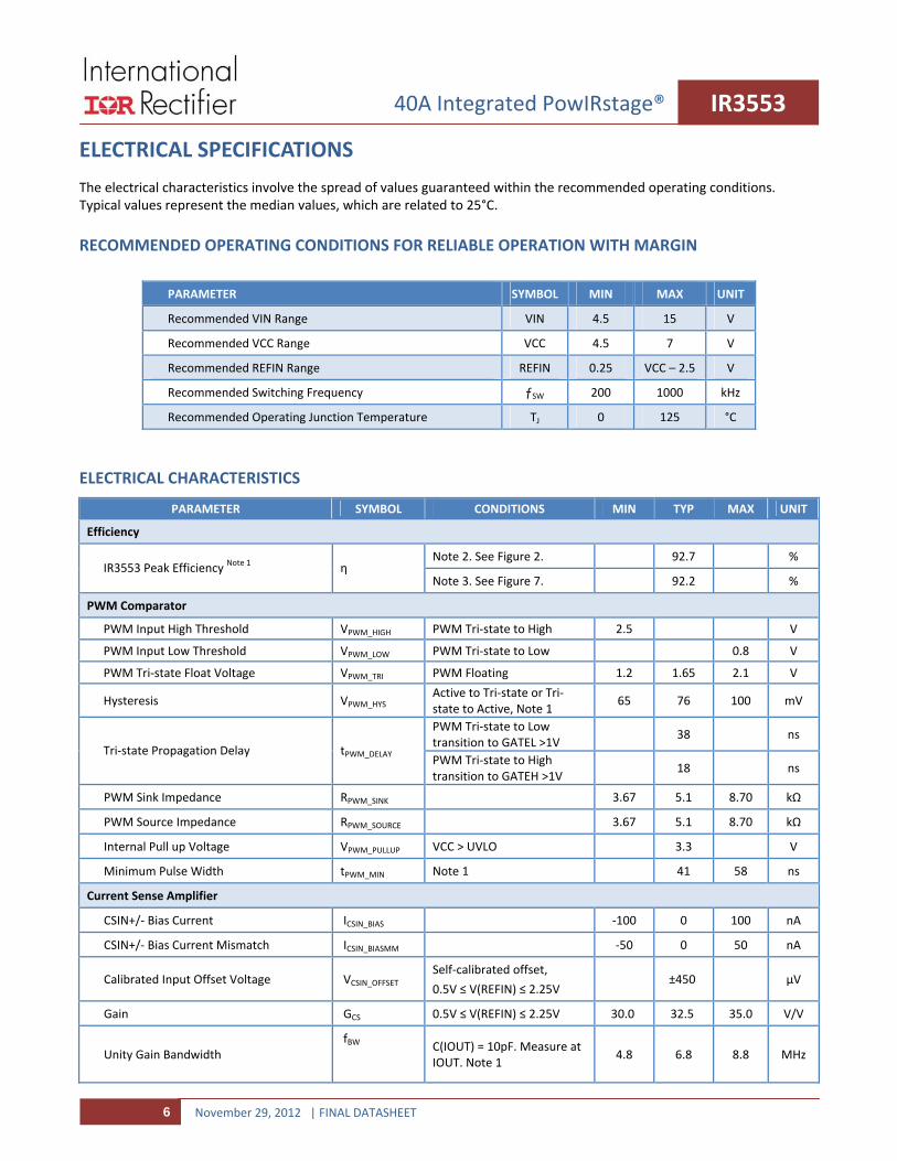
ELECTRICAL SPECIFICATIONS The electrical characteristics involve the spread of values guaranteed within the recommended operating conditions. Typical values represent the median values, which are related to 25°C.
RECOMMENDED OPERATING CONDITIONS FOR RELIABLE OPERATION WITH MARGIN
PARAMETER SYMBOL MIN MAX UNIT
Recommended VIN Range VIN 4.5 15 V
Recommended VCC Range VCC 4.5 7 V
Recommended REFIN Range REFIN 0.25 VCC – 2.5 V
Recommended Switching Frequency ƒSW 200 1000 kHz
Recommended Operating Junction Temperature TJ 0 125 °C
ELECTRICAL CHARACTERISTICS
PARAMETER SYMBOL CONDITIONS MIN TYP MAX UNIT
Efficiency
Note 2. See Figure 2. 92.7 % IR3553 Peak Efficiency Note 1 η
Note 3. See Figure 7. 92.2 %
PWM Comparator
PWM Input High Threshold VPWM_HIGH PWM Tri‐state to High 2.5 V
PWM Input Low Threshold VPWM_LOW PWM Tri‐state to Low 0.8 V
PWM Tri‐state Float Voltage VPWM_TRI PWM Floating 1.2 1.65 2.1 V
Hysteresis VPWM_HYS Active to Tri‐state or Tri‐state to Active, Note 1
65 76 100 mV
PWM Tri‐state to Low transition to GATEL >1V
38 ns Tri‐state Propagation Delay tPWM_DELAY
PWM Tri‐state to High transition to GATEH >1V
18 ns
PWM Sink Impedance RPWM_SINK 3.67 5.1 8.70 kΩ
PWM Source Impedance RPWM_SOURCE 3.67 5.1 8.70 kΩ
Internal Pull up Voltage VPWM_PULLUP VCC > UVLO 3.3 V
Minimum Pulse Width tPWM_MIN Note 1 41 58 ns
Current Sense Amplifier
CSIN+/‐ Bias Current ICSIN_BIAS ‐100 0 100 nA
CSIN+/‐ Bias Current Mismatch ICSIN_BIASMM ‐50 0 50 nA
Calibrated Input Offset Voltage VCSIN_OFFSET Self‐calibrated offset,
0.5V ≤ V(REFIN) ≤ 2.25V ±450 µV
Gain GCS 0.5V ≤ V(REFIN) ≤ 2.25V 30.0 32.5 35.0 V/V
Unity Gain Bandwidth fBW
C(IOUT) = 10pF. Measure at IOUT. Note 1
4.8 6.8 8.8 MHz

November 29, 2012 | FINAL DATASHEET7
IR355340A Integrated PowIRstage®
PARAMETER SYMBOL CONDITIONS MIN TYP MAX UNIT
Slew Rate SR 6 V/µs
Differential Input Range VD_IN 0.8V ≤ V(REFIN) ≤ 2.25V, ‐10 25 mV
Common Mode Input Range VC_IN 0 VCC‐2.5
V
Output Impedance (IOUT) RCS_OUT 62 200 Ω
IOUT Sink Current ICS_SINK Driving external 3 kΩ 0.5 0.8 1.1 mA
Diode Emulation Mode Comparator
Input Offset Voltage VIN_OFFSET Note 1 ‐12 ‐3 3 mV
Leading Edge Blanking Time tBLANK V(GATEL)>1V Starts Timer 50 150 200 ns
Negative Current Time‐Out tNC_TOUT PWM = Tri‐State,
V(SW) ≤ ‐10mV 12 28 46 µs
Digital Input – BBRK#
Input voltage high VBBRK#_IH 2.0 V
Input voltage low VBBRK#_IL 0.8 V
Internal Pull Up Resistance RBBRK#_PULLUP VCC > UVLO 69 200 338 kΩ
Internal Pull Up Voltage VBBRK#_PULLUP VCC > UVLO 3.3 V
Digital Output – PHSFLT#
Output voltage high VPHASFLT#_OH VCC V
Output voltage low VPHASFLT#_OL 4mA 150 300 mV
Input current IPHASFLT#_IN V(PHSFLT#) = 5.5V 0 1 µA
Phase Fault Detection
Control MOSFET Short Threshold VCM_SHORT Measure from SW to PGND 3.3 V
Synchronous MOSFET Short Threshold VSM_SHORT Measure from SW to PGND 150 200 250 mV
Synchronous MOSFET Open Threshold VSM_OPEN Measure from SW to PGND ‐250 ‐200 ‐150 mV
Propagation Delay tPROP PWM High to Low Cycles 15 Cycle
Thermal Flag
Rising Threshold TRISE PHSFLT# Drives Low,
Note 1 160 °C
Falling Threshold TFALL Note 1 135 °C
Bootstrap Diode
Forward Voltage VFWD
I(BOOST) = 30mA, VCC = 6.8V
360 520 920 mV
VCC Under Voltage Lockout
Start Threshold VVCC_START 3.3 3.7 4.1 V
Stop Threshold VVCC_STOP 3.0 3.4 3.8 V
Hysteresis VVCC_HYS 0.2 0.3 0.4 V
General

November 29, 2012 | FINAL DATASHEET8
IR355340A Integrated PowIRstage®
PARAMETER SYMBOL CONDITIONS MIN TYP MAX UNIT
VCC Supply Current IVCC VCC = 4.5V to 7V 4 8 12 mA
VIN Supply Leakage Current IVIN VIN = 20V, 125C, V(PWM) = Tri‐State
1 µA
BOOST Supply Current IBOOST 4.75V < V(BOOST)‐V(SW) < 8V
0.5 1.5 3.0 mA
REFIN Bias Current IREFIN ‐1.5 0 1 µA
SW Floating Voltage VSW_FLOAT V(PWM) = Tri‐State 0.2 0.4 V
SW Pull Down Resistance RSW_PULLDOWN BBRK# is Low or VCC = 0V 18 kΩ
Notes
1. Guaranteed by design but not tested in production
2. VIN=12V, VOUT=1.2V, ƒSW = 300kHz, L=210nH (0.2mΩ), VCC=6.8V, CIN=47uF x 4, COUT =470uF x3, 400LFM airflow, no heat sink, 25°C ambient temperature, and 8‐layer PCB of 3.7” (L) x 2.6” (W). PWM controller loss and inductor loss are not included.
3. VIN=12V, VOUT=1.2V, ƒSW = 400kHz, L=150nH (0.29mΩ), VCC=7V, CIN=47uF x 4, COUT =470uF x3, no airflow, no heat sink, 25°C ambient temperature, and 8‐layer PCB of 3.7” (L) x 2.6” (W). PWM controller loss and inductor loss are not included.

November 29, 2012 | FINAL DATASHEET9
IR355340A Integrated PowIRstage®
TYPICAL OPERATING CHARACTERISTICS Circuit of Figure 32, VIN=12V, VOUT=1.2V, ƒSW = 400kHz, L=150nH (0.29mΩ), VCC=7V, TAMBIENT = 25°C, no heat sink, no air flow, 8‐layer PCB board of 3.7” (L) x 2.6” (W), no PWM controller loss, no inductor loss, unless specified otherwise.
Figure 7: Typical IR3553 Efficiency
Figure 8: Typical IR3553 Power Loss
Figure 9: Safe Operating Area, TCASE <= 125°C
Figure 10: Normalized Power Loss vs. Input Voltage
Figure 11: Normalized Power Loss vs. Output Voltage
Figure 12: Normalized Power Loss vs. Switching Frequency
80
81
82
83
84
85
86
87
88
89
90
91
92
93
0 5 10 15 20 25 30 35 40
Output Current (A)
Efficiency (%)
0
1
2
3
4
5
6
7
8
9
10
0 5 10 15 20 25 30 35 40
Output Current (A)
Power Loss (W)
0
5
10
15
20
25
30
35
40
45
0 5 10 15 20 25 30 35 40 45 50 55 60 65 70 75 80 85 90
Ambient Temperature (°C)
Output Current (A)
400LFM
200LFM
100LFM
0LFM
0.80
0.85
0.90
0.95
1.00
1.05
1.10
1.15
1.20
1.25
1.30
5 6 7 8 9 10 11 12 13 14 15
Input Voltage (V)
Normalized Pow
er Loss
‐6.0
‐4.5
‐3.0
‐1.5
0.0
1.5
3.0
4.5
6.0
7.5
9.0
Case Tem
perature Adjustment (°C)
0.8
0.9
1.0
1.1
1.2
1.3
1.4
1.5
0.8 0.9 1 1.1 1.2 1.3 1.4 1.5 1.6 1.7 1.8 1.9 2
Output Voltage (V)
Normalized Pow
er Loss
‐6
‐3
0
3
6
9
12
15
Case Temperature Adjustmen
t (°C)
0.80
0.85
0.90
0.95
1.00
1.05
1.10
1.15
1.20
1.25
1.30
200 300 400 500 600 700 800 900 1000
Switching Frequency (kHz)
Norm
alized
Power Loss
‐6.0
‐4.5
‐3.0
‐1.5
0.0
1.5
3.0
4.5
6.0
7.5
9.0
Case Tem
perature Adjustm
ent (°C)

November 29, 2012 | FINAL DATASHEET10
IR355340A Integrated PowIRstage®
TYPICAL OPERATING CHARACTERISTICS (CONTINUED) Circuit of Figure 32, VIN=12V, VOUT=1.2V, ƒSW = 400kHz, L=150nH (0.29mΩ), VCC=7V, TAMBIENT = 25°C, no heat sink, no air flow, 8‐layer PCB board of 3.7” (L) x 2.6” (W), no PWM controller loss, no inductor loss, unless specified otherwise.
Figure 13: Normalized Power Loss vs. VCC Voltage
Figure 14: Power Loss vs. Output Inductor
Figure 15: VCC Current vs. Switching Frequency
Figure 16: Switching Waveform, IOUT = 0A
Figure 17: Switching Waveform, IOUT = 40A
Figure 18: PWM to SW Delays, IOUT = 10A
PWM 2V/div
SW 5V/div
40ns/div
PWM 5V/div
SW 5V/div
GATEL 10V/div
400ns/div
PWM 5V/div
SW 5V/div
GATEL 10V/div
400ns/div
0
10
20
30
40
50
60
200 300 400 500 600 700 800 900 1000
fsw (kHz)
VCC Current (m
A)
Vcc=6.8V
Vcc=5V
0.80
0.85
0.90
0.95
1.00
1.05
1.10
1.15
1.20
1.25
1.30
5.00 5.25 5.50 5.75 6.00 6.25 6.50 6.75 7.00
VCC Voltage (V)
Norm
alized
Power Loss
‐6.0
‐4.5
‐3.0
‐1.5
0.0
1.5
3.0
4.5
6.0
7.5
9.0
Case Temperature Adjustmen
t (°C)
0.80
0.85
0.90
0.95
1.00
1.05
1.10
1.15
1.20
1.25
1.30
120 130 140 150 160 170 180 190 200 210
Output Inductor (nH)
Norm
alized
Power Loss
‐6.0
‐4.5
‐3.0
‐1.5
0.0
1.5
3.0
4.5
6.0
7.5
9.0
Case Temperature Adjustmen
t (°C)

November 29, 2012 | FINAL DATASHEET11
IR355340A Integrated PowIRstage®
TYPICAL OPERATING CHARACTERISTICS (CONTINUED) Circuit of Figure 32, VIN=12V, VOUT=1.2V, ƒSW = 400kHz, L=150nH (0.29mΩ), VCC=7V, TAMBIENT = 25°C, no heat sink, no air flow, 8‐layer PCB board of 3.7” (L) x 2.6” (W), no PWM controller loss, no inductor loss, unless specified otherwise.
Figure 19: Body‐Braking® Delays
Figure 20: PWM Tri‐state Delays, IOUT = 10A
Figure 21: PWM Tri‐state Delays, IOUT = 10A
Figure 22: Diode Emulation Mode, IOUT = 3A
Figure 23: Body‐Braking® Mode, IOUT = 3A
Figure 24: Diode Emulation Setup through BBRK# Capacitor
VCC 2V/div
BBRK# 1V/div
2ms/div
SW 10V/div
BBRK# 5V/div
GATEL 5V/div
40ns/div
PWM 5V/div
PWM 2V/div
SW 5V/div
100ns/div
PWM 2V/div
SW 5V/div
100ns/div
PWM 2V/div
SW 5V/div
400ns/div
GATEL 10V/div
PWM 2V/div
SW 5V/div
400ns/div
GAETL 10V/div

November 29, 2012 | FINAL DATASHEET12
IR355340A Integrated PowIRstage®
TYPICAL OPERATING CHARACTERISTICS (CONTINUED) Circuit of Figure 32, VIN=12V, VOUT=1.2V, ƒSW = 400kHz, L=150nH (0.29mΩ), VCC=7V, TAMBIENT = 25°C, no heat sink, no air flow, 8‐layer PCB board of 3.7” (L) x 2.6” (W), no PWM controller loss, no inductor loss, unless specified otherwise.
Figure 25: Diode Emulation Setup through BBRK# Input
Figure 26: Diode Emulation Setup through BBRK# Input
Figure 27: Current Sense Amplifier Output vs. Current
Figure 28: Current Sense Amplifier Output, IOUT = 0A
Figure 29: Current Sense Amplifier Output, IOUT = 20A
Figure 30: Current Sense Amplifier Output, IOUT = 20A, 300kHz
0.00
0.05
0.10
0.15
0.20
0.25
0.30
0.35
0.40
0.45
0.50
0 5 10 15 20 25 30 35 40
Output Current (A)
IOUT‐REFIN (V)
VCC 2V/div
BBRK# 2V/div
4ms/div
VCC 2V/div
BBRK# 2V/div
4ms/div
V(IOUT)‐V(REFIN) 0.2V/div
IL 10A/div
2us/div
SW 20V/div
V(IOUT)‐V(REFIN) 0.2V/div
IL 10A/div
2us/div
SW 20V/div
V(IOUT)‐V(REFIN) 0.2V/div
IL 10A/div
2us/div
SW 20V/div

November 29, 2012 | FINAL DATASHEET13
IR355340A Integrated PowIRstage®
THEORY OF OPERATION
DESCRIPTION
The IR3553 PowIRstage® is a synchronous buck driver with co‐packed MOSFETs with integrated Schottky diode, which provides system designers with ease of use and flexibility required in cutting edge CPU, GPU and DDR memory power delivery designs and other high‐current low‐profile applications.
The IR3553 is designed to work with a PWM controller. It incorporates a continuously self‐calibrated current sense amplifier, optimized for use with inductor DCR sensing. The current sense amplifier provides signal gain and noise immunity, supplying multiphase systems with a superior design toolbox for programmed impedance designs.
The IR3553 provides a phase fault signal capable of detecting open or shorted MOSFETs, or an over‐temperature condition in the vicinity of the power stage.
The IR3553 accepts an active low Body‐Braking® input which disables both MOSFETs to enhance transient performance or provide a high impedance output.
The IR3553 provides diode emulation feature which avoids negative current in the synchronous MOSFET and improves light load efficiency.
The IR3553 PWM input is compatible with 3.3V logic signal and 7V tolerant. It accepts 3‐level PWM input signals with tri‐state.
PWM TRI‐STATE INPUT
The IR3553 PWM accepts 3‐level input signals. When PWM input is high, the synchronous MOSFET is turned off and the control MOSFET is turned on. When PWM input is low, control MOSFET is turned off and synchronous MOSFET is turned on. Figures 16‐18 show the PWM input and the corresponding SW and GATEL output of the IR3553. If PWM pin is floated , the built‐in resistors pull the PWM pin into a tri‐state region centered around 1.65V.
When PWM input is in tri‐state, two operation modes can be selected by controlling BBRK# input. If the BBRK# input is always high, the default operation mode is Body‐ Braking®, in which both MOSFETs will be turned off when the PWM input is in tri‐state. If the BBRK# input has been pulled low for at least 20ns after the VCC passes its UVLO threshold during power up, the diode emulation mode is
set. PWM input in tri‐state will activate a synchronous diode emulation feature allowing designers to maximize system efficiency at light loads without compromising transient performance.
BODY‐BRAKING® MODE
International Rectifier’s Body‐Braking® is a operation mode in which two MOSFETs are turned off. When the synchronous MOSFET is off, the higher voltage across the Shottky diode in parallel helps discharging the inductor current faster, which reduces the output voltage overshoot. The Body‐Braking® can be used either to enhance transient response of the converter after load release or to provide a high impedance output.
There are two ways to place the IR3553 in Body‐Braking® mode, either controlling the BBRK# pin directly or through a PWM tri‐state signal. Both control signals are usually from the PWM controller.
Pulling BBRK# low forces the IR3553 into Body‐Braking® mode rapidly, which is usually used to enhance converter transient response after load release, as shown in Figure 19. Releasing BBRK# forces the IR3553 out of Body‐ Braking® mode quickly.
The BBRK# low turns off both MOSFETs and therefore can also be used to disable/enable a converter.
If the BBRK# input is always high, the Body‐Braking® is activated when the PWM input enters the tri‐state region, as shown in Figures 20 and 21. Comparing to pulling down the BBRK# pin directly, the Body‐Braking® response to PWM tri‐state signal is slower due to the hold‐off time created by the PWM pin parasitic capacitor with the pull‐up and pull‐down resistors of PWM pin. For better performance, no more than 100pF parasitic capacitive load should be present on the PWM line of IR3553.
SYNCHRONOUS DIODE EMULATION MODE
An additional feature of the IR3553 is the synchronous diode emulation mode. This function enables increased efficiency by preventing negative inductor current from flowing in the synchronous MOSFET.
As shown in Figure 22, when the PWM input enters the tri‐state region the control MOSFET is turned off first, and the synchronous MOSFET is initially turned on and then is turned off when the output current reaches zero. If the sensed output current does not reach zero within a set amount of time the gate driver will assume that the output

November 29, 2012 | FINAL DATASHEET14
IR355340A Integrated PowIRstage®
is de‐biased and turn off the synchronous MOSFET, allowing the switch node to float.
This is in contrast to the Body‐Braking® mode shown in Figure 23, where GATEL follows PWM input. The Schottky diode in parallel with the synchronous MOSFET conducts for a longer period of time and therefore lowers the light load efficiency.
The zero current detection circuit in the IT3553 is independent of the current sense amplifier and therefore still functions even if the current sense amplifier is not used. As shown in Figure 6, an offset is added to the diode emulation comparator so that a slightly positive output current in the inductor and synchronous MOSFET is treated as zero current to accommodate propagation delays, preventing any negative current flowing in the synchronous MOSFET. This causes the Schottky diode in parallel with the synchronous MOSFET to conduct before the inductor current actually reaches zero, and the conduction time increases with inductance of the output inductor.
To set the IR3553 in diode emulation mode, the BBRK# pin must be toggled low at least once after the VCC passes its UVLO threshold during power up. One simple way is to use the internal BBRK# pull‐up resistor (200kΩ typical) with an external capacitor from BBRK# pin to LGND, as shown in Figure 4. To ensure the diode emulation mode is properly set, the BBRK# voltage should be lower than 0.8V when the VCC voltage passes its UVLO threshold (3.3V minimum and 3.7V typical), as shown in Figure 24. A digital signal from the PWM controller can also be used to set the diode emulation mode. The BBRK# signal can either be pulled low for at least 20ns after the VCC passes its UVLO threshold, as shown in Figure 25, or be pulled low before VCC power up and then released after the VCC passes its UVLO threshold, as shown in Figure 26.
Once the diode emulation mode is set, it cannot be reset until the VCC power is recycled.
PHASE FAULT AND THERMAL FLAG OUTPUT
The phase fault circuit looks at the switch node with respect to ground to determine whether there is a defective MOSFET in the phase. The output of the phase fault signal is high during normal operation and is pulled low when there is a fault. Each driver monitors the MOSFET it drives. If the switch node is less than a certain voltage above ground when the PWM signal goes low or if the switch node is a certain voltage above ground when the PWM signal rises, this gives a fault signal. If there are a
number of consecutive faults the phase fault signal is asserted.
Thermal flag circuit monitors the temperature of the IR3553. If the temperature goes above a threshold (160°C typical) the PHSFLT# pin is pulled low after a maximum delay of 100us.
The PHSFLT# pin can be pulled low by either the phase fault circuit or the thermal flag circuit. The phase fault signal could be used to turn off the AC/DC converter or blow a fuse to disconnect the DC/DC converter input from the supply.
If PHSFLT# is not used it can be floated or connected to LGND.
LOSSLESS AVERAGE INDUCTOR CURRENT
SENSING
Inductor current can be sensed by connecting a series resistor and a capacitor network in parallel with the inductor and measuring the voltage across the capacitor, as shown in Figure 31.
SW
VIN
CSIN+
CSIN‐
IR3553 VIN
VOUT
CIN
CCS
L
COUTRCS
RL
‐+
iL
+ vCS ‐Current Sense
Amplifier
+ vL ‐
Figure 31: Inductor current sensing
The equation of the current sensing network is as follows.
CSCS
LLL
CSCSLCS CsR
R
Ls
RsiCsR
svsv
1
1)(
1
1)()(
LL Rsi )(
CSCSL CRRLwhen
Usually the resistor RCS and capacitor CCS are chosen so that the time constant of RCS and CCS equals the inductor time

November 29, 2012 | FINAL DATASHEET15
IR355340A Integrated PowIRstage®
constant, which is the inductance L over the inductor DCR (RL). If the two time constants match, the voltage across CCS is proportional to the current through L, and the sense circuit can be treated as if only a sense resistor with the value of RL was used. The mismatch of the time constants does not affect the measurement of inductor DC current, but affects the AC component of the inductor current.
The advantage of sensing the inductor current versus high side or low side sensing is that actual output current being delivered to the load is obtained rather than peak or sampled information about the switch currents. The output voltage can be positioned to meet a load line based on real time information. This is the only sense method that can support a single cycle transient response. Other methods provide no information during either load increase (low side sensing) or load decrease (high side sensing).
CURRENT SENSE AMPLIFIER
A high speed differential current sense amplifier is located in the IR3553, as shown in Figure 6. Its gain is nominally 32.5, and the inductor DCR increase with temperature is not compensated inside the IR3553. The current sense amplifier output IOUT is referenced to REFIN, which is usually connected to a reference voltage from the PWM controller. Figure 27 shows the differential voltage of V(IOUT) – V(REFIN) versus the inductor current and reflects the inductor DCR increase with temperature at higher current.
The current sense amplifier can accept positive differential input up to 25mV and negative input up to ‐10mV before clipping. The output of the current sense amplifier is summed with the reference voltage REFIN and sent to the IOUT pin. The REFIN voltage is to ensure at light loads there is enough output range to accommodate the negative current ripple shown in Figure 28. In a multiphase converter, the IOUT pins of all the phases can be tied together through resistors, and the IOUT voltage represents the average current through all the inductors and is used by the controller for adaptive voltage positioning.
The input offset voltage is the primary source of error for the current signal. In order to obtain very accurate current signal, the current sense amplifier continuously calibrates itself, and the input offset of this amplifier is within +/‐ 450uV. This calibration algorithm can create a small ripple on IOUT with a frequency of fsw/128.
If the IR3553 current sense amplifier is required, connect its output IOUT and the reference voltage REFIN to the PWM controller and connect the inductor sense circuit as shown in Figure 4. If the current sense amplifier is not needed, tie CSIN+, CSIN‐ and REFIN pins to LGND and float IOUT pin, as shown in Figure 5.
DESIGN PROCEDURES
POWER LOSS CALCULATION
The single‐phase IR3553 efficiency and power loss measurement circuit is shown in Figure 32.
SW
VIN
PGND
VCC
BOOSTPWM
CSIN+
CSIN‐
LGND
IOUT
BBRK#
REFIN
IR3553
PHSFLT#
VIN
VOUT
C247uF x4
C50.22uF
C40.22uF
R22.49k
L1150nH
C6470uF x3
C10.1uF x2
VCC
R110k
IVCC IIN
IOUT
C31uF
C71nF
VSW
Figure 32: IR3553 Power Loss Measurement
The IR3553 power loss is determined by,
OUTSWVCCCCININLOSS IVIVIVP
Where both MOSFET loss and the driver loss are included, but the PWM controller and the inductor losses are not.
Figure 7 shows the measured single‐phase IR3553 efficiency under the default test conditions, VIN=12V, VOUT=1.2V, ƒSW = 400kHz, L=150nH (0.29mΩ), VCC=7V, TAMBIENT = 25°C, no heat sink, and no air flow.
The efficiency of an interleaved multiphase IR3553 converter is always higher than that of a single‐phase under the same conditions due to the reduced input RMS current and more input/output capacitors.
The measured single‐phase IR3553 power loss under the same conditions is provided in Figure 8.

November 29, 2012 | FINAL DATASHEET16
IR355340A Integrated PowIRstage®
If any of the application condition, i.e. input voltage, output voltage, switching frequency, VCC MOSFET driver voltage or inductance, is different from those of Figure 8, a set of normalized power loss curves should be used. Obtain the normalizing factors from Figure 10 to Figure 14 for the new application conditions; multiply these factors by the power loss obtained from Figure 8 for the required load current.
As an example, the power loss calculation procedures under different conditions, VIN=10V, VOUT=1V, ƒSW = 300kHz, VCC=5V, L=210nH, VCC=5V, IOUT=30A, TAMBIENT = 25°C, no heat sink, and no air flow, are as follows.
1) Determine the power loss at 30A under the default test conditions of VIN=12V, VOUT=1.2V, ƒSW = 400kHz, L=150nH, VCC=7V, TAMBIENT = 25°C, no heat sink, and no air flow. It is 4.7W from Figure 8.
2) Determine the input voltage normalizing factor with VIN=10V, which is 1.02 based on the dashed lines in Figure 10.
3) Determine the output voltage normalizing factor with VOUT=1V, which is 0.90 based on the dashed lines in Figure 11.
4) Determine the switching frequency normalizing factor with ƒSW = 300kHz, which is 0.99 based on the dashed lines in Figure 12.
5) Determine the VCC MOSFET drive voltage normalizing factor with VCC=5V, which is 1.18 based on the dashed lines in Figure 13.
6) Determine the inductance normalizing factor with L=210nH, which is 0.94 based on the dashed lines in Figure 14.
7) Multiply the power loss under the default conditions by the five normalizing factors to obtain the power loss under the new conditions, which is 4.7W x 1.02 x 0.90 x 0.99 x 1.18 x 0.94 = 4.74W.
SAFE OPERATING AREA
Figure 9 shows the IR3553 safe operating area with the case temperature controlled at or below 125°C. The test conditions are VIN=12V, VOUT=1.2V, ƒSW=400kHz, L=150nH (0.29mΩ), VCC=7V, TAMBIENT = 0°C to 90°C, no heat sink, and Airflow = 0LFM / 100LFM / 200LFM / 400LFM.
If any of the application condition, i.e. input voltage, output voltage, switching frequency, VCC MOSFET driver voltage, or inductance is different from those of Figure 9, a set of IR3553 case temperature adjustment curves should be used. Obtain the temperature deltas from Figure 10 to Figure 14 for the new application conditions; sum these deltas and then subtract from the IR3553 case temperature obtained from Figure 9 for the required load current.
8) From Figure 9, determine the highest ambient temperature at the required load current under the default conditions, which is 66°C at 30A with 0LFM airflow and the IR3553 case temperature of 125°C.
9) Determine the case temperature with VIN=10V, which is +0.6° based on the dashed lines in Figure 10.
10) Determine the case temperature with VOUT=1V, which is ‐3.0° based on the dashed lines in Figure 11.
11) Determine the case temperature with ƒSW = 300kHz, which is ‐0.4° based on the dashed lines in Figure 12.
12) Determine the case temperature with VCC = 5V, which is +5.4° based on the dashed lines in Figure 13.
13) Determine the case temperature with L=210nH, which is ‐1.8° based on the dashed lines in Figure 14.
14) Sum the case temperature adjustment from 9) to 13), +0.6° ‐3.0° ‐0.4° +5.4° ‐1.8° = +0.8°. Deduct the delta from the highest ambient temperature in step 8), 66°C – (+0.8°C) = 65.2°C.
INDUCTOR CURRENT SENSING CAPACITOR CCS AND RESISTOR RCS
If the IR3553 is used with inductor DCR sensing, care must be taken in the printed circuit board layout to make a Kelvin connection across the inductor DCR. The DC resistance of the inductor is utilized to sense the inductor current. Usually the resistor RCS and capacitor CCS in parallel with the inductor are chosen to match the time constant of the inductor, and therefore the voltage across the capacitor CCS represents the inductor current.
Measure the inductance L and the inductor DC resistance RL. Pre‐select the capacitor CCS and calculate RCS as follows.
CS
LCS C
RLR

November 29, 2012 | FINAL DATASHEET17
IR355340A Integrated PowIRstage®
INPUT CAPACITORS CVIN
At least two 10uF 1206 ceramic capacitors and one 0.1uF 0402 ceramic capacitor are recommended for decoupling the VIN to PGND connection. The 0.1uF 0402 capacitor should be on the same side of the PCB as the IR3553 and next to the VIN and PGND pins. Adding additional capacitance and use of capacitors with lower ESR and mounted with low inductance routing will improve efficiency and reduce overall system noise, especially in single‐phase designs or during high current operation.
BOOTSTRAP CAPACITOR CBOOST
A minimum of 0.22uF 0402 capacitor is required for the bootstrap circuit. A high temperature 0.22uF or greater value 0402 capacitor is recommended. It should be mounted on the same side of the PCB as the IR3553 and as close as possible to the BOOST pin. A low inductance routing of the SW pin connection to the other terminal of the bootstrap capacitor is strongly recommended.
VCC DECOUPLING CAPACITOR CVCC
A 0.1uF to 1uF ceramic decoupling capacitor is required at the VCC pin. It should be mounted on the same side of the PCB as the IR3553 and as close as possible to the VCC and PGND (pin 4). Low inductance routing between the VCC capacitor and the IR3553 pins is strongly recommended.
BODY‐BRAKING® FEATURE
The BBRK# pin should be pulled up to VCC if the feature is not used by the PWM controller. Use of a small value resistor or a direct connection to VCC is recommended.
MOUNTING OF HEAT SINKS
Care should be taken in the mounting of heat sinks so as not to short‐circuit nearby components. The VCC and Bootstrap capacitors are typically mounted on the same side of the PCB as the IR3553. The mounting height of these capacitors must be considered when selecting their package sizes.
HIGH OUTPUT VOLTAGE DESIGN
CONSIDERATIONS
The IR3553 is capable of creating output voltages above the 3.3V recommended maximum output voltage as there are no restrictions inside the IR3553 on the duty cycle applied to the PWM pin. However if the current sense feature is required, the common mode range of the
current sense amplifier inputs must be considered. A violation of the current sense input common mode range may cause unexpected IR3553 behavior. Also the output current rating of the device will be reduced as the duty cycle increases. In very high duty cycle applications sufficient time must be provided for replenishment of the Bootstrap capacitor for the control MOSFET drive.
LAYOUT EXAMPLE
Contact International Rectifier for a layout example suitable for your specific application.

November 29, 2012 | FINAL DATASHEET18
IR355340A Integrated PowIRstage®
METAL AND COMPONENT PLACEMENT
Lead land width should be equal to nominal part lead width. The minimum lead to lead spacing should be ≥ 0.2mm to prevent shorting.
Lead land length should be equal to maximum part lead length +0.15 ‐ 0.3 mm outboard extension and 0 to + 0.05mm inboard extension. The outboard extension ensures a large and visible toe fillet, and the inboard extension will accommodate any part misalignment and ensure a fillet.
Center pad land length and width should be equal to maximum part pad length and width.
Only 0.30mm diameter via shall be placed in the area of the power pad lands and connected to power planes to minimize the noise effect on the IC and to improve thermal performance.
23
16
171819202122
25
245
4
3
2
1
111098
15
14
13
12
7
6
Figure 33: Metal and component placement
* Contact International Rectifier to receive an electronic PCB Library file in Cadence Allegro or CAD DXF/DWG format.

November 29, 2012 | FINAL DATASHEET19
IR355340A Integrated PowIRstage®
SOLDER RESIST
The solder resist should be pulled away from the metal lead lands by a minimum of 0.06mm. The solder resist miss‐alignment is a maximum of 0.05mm and it is recommended that the low power signal lead lands are all Non Solder Mask Defined (NSMD). Therefore pulling the S/R 0.06mm will always ensure NSMD pads.
The minimum solder resist width is 0.13mm typical.
At the inside corner of the solder resist where the lead land groups meet, it is recommended to provide a fillet so a solder resist width of ≥ 0.17mm remains.
The dimensions of power land pads, VIN, PGND, TGND and SW, are Non Solder Mask Defined (NSMD). The equivalent PCB layout becomes Solder Mask Defined (SMD) after power shape routing.
Ensure that the solder resist in‐between the lead lands and the pad land is ≥ 0.15mm due to the high aspect ratio of the solder resist strip separating the lead lands from the pad land.
Figure 34: Solder resist
* Contact International Rectifier to receive an electronic PCB Library file in Cadence Allegro or CAD DXF/DWG format.

November 29, 2012 | FINAL DATASHEET20
IR355340A Integrated PowIRstage®
STENCIL DESIGN
The stencil apertures for the lead lands should be approximately 65% to 75% of the area of the lead lands depending on stencil thickness. Reducing the amount of solder deposited will minimize the occurrence of lead shorts. Since for 0.5mm pitch devices the leads are only 0.25mm wide, the stencil apertures should not be made narrower; openings in stencils < 0.25mm wide are difficult to maintain repeatable solder release.
The low power signal stencil lead land apertures should therefore be shortened in length to keep area ratio of 65% to 75% while centered on lead land.
The power pads VIN, PGND, TGND and SW, land pad apertures should be approximately 65% to 75% area of solder on the center pad. If too much solder is deposited on the center pad the part will float and the lead lands will be open. Solder paste on large pads is broken down into small sections with a minimum gap of 0.2mm between allowing for out‐gassing during solder reflow.
The maximum length and width of the land pad stencil aperture should be equal to the solder resist opening minus an annular 0.2mm pull back to decrease the incidence of shorting the center land to the lead lands when the part is pushed into the solder paste.
Figure 35: Stencil design
* Contact International Rectifier to receive an electronic PCB Library file in Cadence Allegro or CAD DXF/DWG format.
November 29, 2012 | FINAL DATASHEET21
IR355340A Integrated PowIRstage®
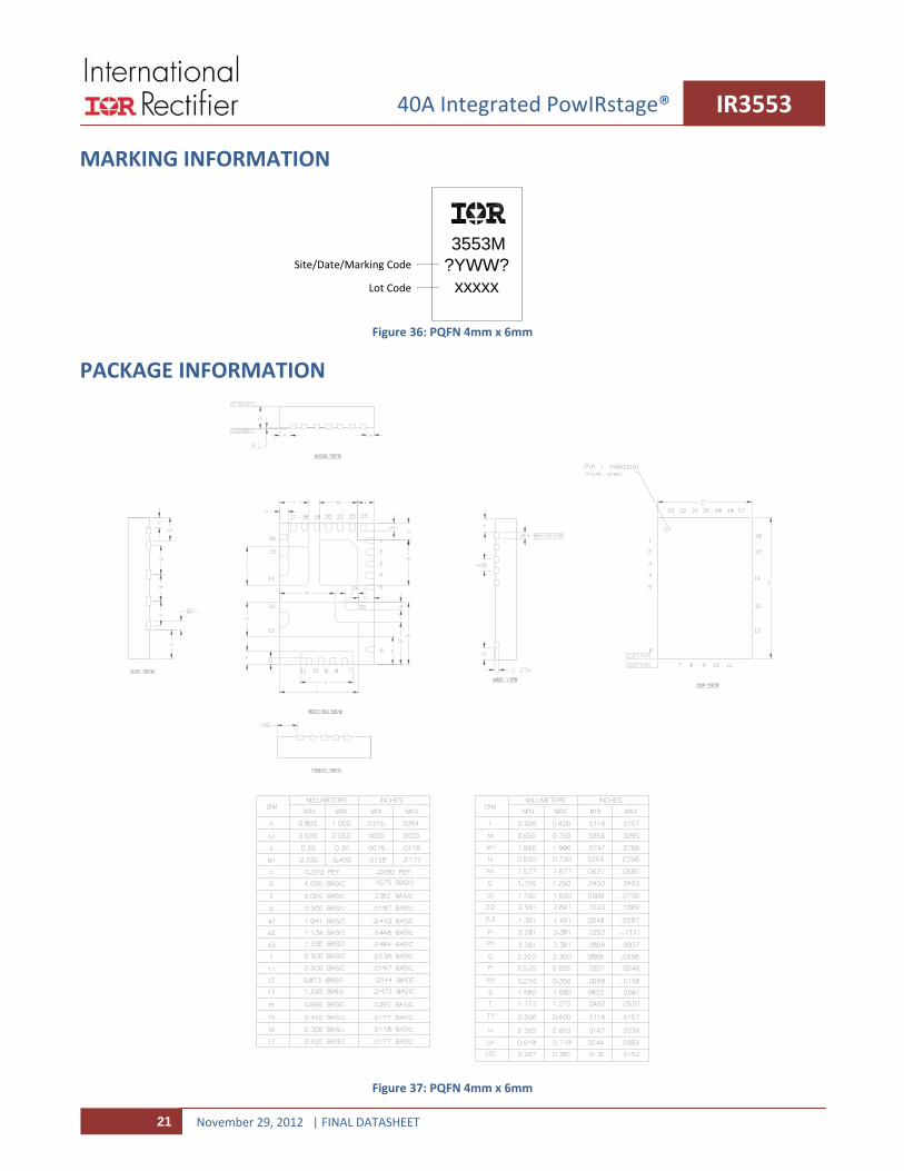
MARKING INFORMATION
Figure 36: PQFN 4mm x 6mm
PACKAGE INFORMATION
Figure 37: PQFN 4mm x 6mm
3553M?YWW?
xxxxxSite / Date/ Marking Code
Lot Code

November 29, 2012 | FINAL DATASHEET22
IR355340A Integrated PowIRstage®
Data and specifications subject to change without notice. This product will be designed and qualified for the Industrial market.
Qualification Standards can be found on IR’s Web site.
IR WORLD HEADQUARTERS: 233 Kansas St., El Segundo, California 90245, USA Tel: (310) 252‐7105 TAC Fax: (310) 252‐7903
Visit us at www.irf.com for sales contact information. www.irf.com