3kw and 5kw half-bridge class-d rf … #9300-0008 rev 1 directed energy, inc. 2002 3kw and 5kw...
TRANSCRIPT

Doc #9300-0008 Rev 1 Directed Energy, Inc. 2002
3kW AND 5kW HALF-BRIDGE CLASS-D RF GENERATORS AT 13.56MHz WITH 89% EFFICENCY AND LIMITED FREQUENCY AGILITY
Abstract DEI / IXYS has developed an RF generator design for very high power at a ISM frequency. of 13.56MHz, using a pair of DE375-102N12A MOSFETS driven by DEIC420 gate drive ICs, in a half-bridge operating in Class-D with limited frequency agility, to generate 3kW of output power at 83.5% efficiency. A pair of modules generates 5KW at 89% efficiency using a total of four DE375-102N12A RF MOSFETs. This technical note discussed the design of this RF generator and supporting SPICE models.
D I R E C T E D E N E R G Y , I N C . T E C H N I C A L N O T E
Directed Energy, Inc. An IXYS Company
2401 Research Blvd. Suite 108 Fort Collins, CO USA 80526 TEL (970) 493-1901 FAX (970) 493-1903 EMAIL: [email protected] www.directedenergy.com

1 Doc #9300-0008 Rev 1
Directed Energy, Inc. 2002
INTRODUCTION Many industrial processes require several kilowatts at one or more of the ISM frequencies. In addition these generators often require some level of frequency agility. Given this need DEI/IXYS has developed a prototype RF generator for very high power RF at ISM frequencies. The prototype generator uses a pair of DE375-102N12A MOSFETS driven by DEIC420 gate drive ICs in a half-bridge topology operating Class-D at 13.56MHz. We have achieved a power output of 3KW at 83.5% efficiency. A pair of modules generates 5KW at 89% efficiency using a total of four DE375-102N12A RF MOSFETs. The design consists of three modules: The gate driver, half-bridge and the output tank. The power output was adjusted via the high voltage supply. Frequency adjustments are made via the input clock. In this paper we will discuss each of the three key sections in detail as well as a complete system spice model. In addition in some applications the generator must be capable of some frequency agility. This capability allows some frequency adjustments to assist in the tuning operation. This topic will also be addressed in each section. The first section is the gate driver. GATE DRIVER (DEI Module #5040-0289B) As in all high frequency topologies, the gate drive section is of vital importance. If the gate driver is not capable of generating narrow gate pulses at high currents, the system’s overall performance will be low. The gate driver presented here is a low-cost, narrow band driver with frequency agility, designed to drive multiple MOSFET devices for RF generator designs in the 2kW to > 10kW range.
2 Doc #9300-0008 Rev 1
Directed Energy, Inc. 2002
C17 0.47
J3SMB VERT JACK
C510.01UF
C7 0.01UF
C35 0.01UF
R15511
C320.47
C25 0.01UF
U3A
74ACT74N
2 3
5
6
144
71
D CLK
Q
Q
VCCPR GNDCL
+ C194.7UF 16V
R131 1W
R250 4BEADS 1/2W
C410.47
C14 0.01UF
C46 0.1UF 200V
C490.01UF
R6A 500 25T
1
3 2
R551.1
VU7
R6500 25T
1
3
2
C26 0.01UF
C500.01UF
U6
501N04A
1
2
3 4 5 6
SG1 GATE SG2 SD2
DRAIN SD1
PHASE ADJ.
+15V
C310.47
J7SMB VERT JACK
R193.32
C470.01UF
C24 0.47
+ C34.7UF 16V
C13 0.47
+VGDV
C21 100PF
+ C3310UF 35V
L1 6uH
C5 0.47
C520.01UF
+5V
R4 220 1/4W
U1A
74ACT74N
2 3
5
6
144
71
D CLK
Q
Q
VCCPR GNDCL
+ C234.7UF 16V
JP1
14(2X7) PIN BERG
1 2 3 4 5 6 7 8 9 10 11 12 13 14
D1MBD301
1
2
C8 680pF
U5 DEIC4201
2
3 4
5
6+VCC
IN
+VCC GND
OUT
GND
R11 1W
J1SMB VERT JACK
C550.01UF
VU3
+5V
C560.01UF
C2 0.1UF 200V
+5V
J2SMB VERT JACK
+15V
C39 0.01UF
U4
501N04A
1
2
3 4 5 6
SG1
GATE SG2 SD2
DRAIN SD1
R30 0 4BEADS 1/2W
C540.01UF
+VGDV
MH3 1 C580.01UF
MH4 1
C45 0.1UF 200V
R231 1/2W
+VGDV
C9 680pF
R281 1W
C27 0.01UF
D2MBD301
1
2
+ C4310UF 35V
C40 0.1UF 200V L2
6uH
C15 0.01UF
U7 DEIC4201
2
3 4
5
6+VCC
IN
+VCC GND
OUT
GND
+5V
R17500 25T
1
3
2
+ C374.7UF 16V
R3511
C570.01UF
+15V
R1651.1
C36 680pF
C530.01UF
R181 1W
C220.47
+15V
C59 100PF
MH1 1
PULSE WIDTH ADJ.
C28 680pF
R12 3.32
C420.47
C34 0.47
C120.47
C11 100PF
PULSE WIDTH ADJ.
C18 0.47
C480.01UF
MH2 1
C10 680pF
U3B
74ACT74N
12 11
9
8
1410
713
D CLK
Q
Q
VCCPR GNDCL
C44 .01UF 200V
+5V C6 0.01UF
R26 0 4BEADS 1/2W
VU3
C16 680pF
C20 0.01UF
C30 680pF
J4SMB VERT JACK
+15V
R11 1K
R83.32
U2 27.12 MHz
4 8
5 GND VCC OUTPUT
C11A 100PF
J5SMB VERT JACK
U1B
74ACT74N
12 11
9 8
14 10
7 13
D CLK
Q Q
VCCPR GND CL
J6SMB VERT JACK
C38 0.01UF
C4 0.01UF
C1.01UF 200V
R9 3.32
C29 680pF
VU7
J8SMB VERT JACK
R10 1K
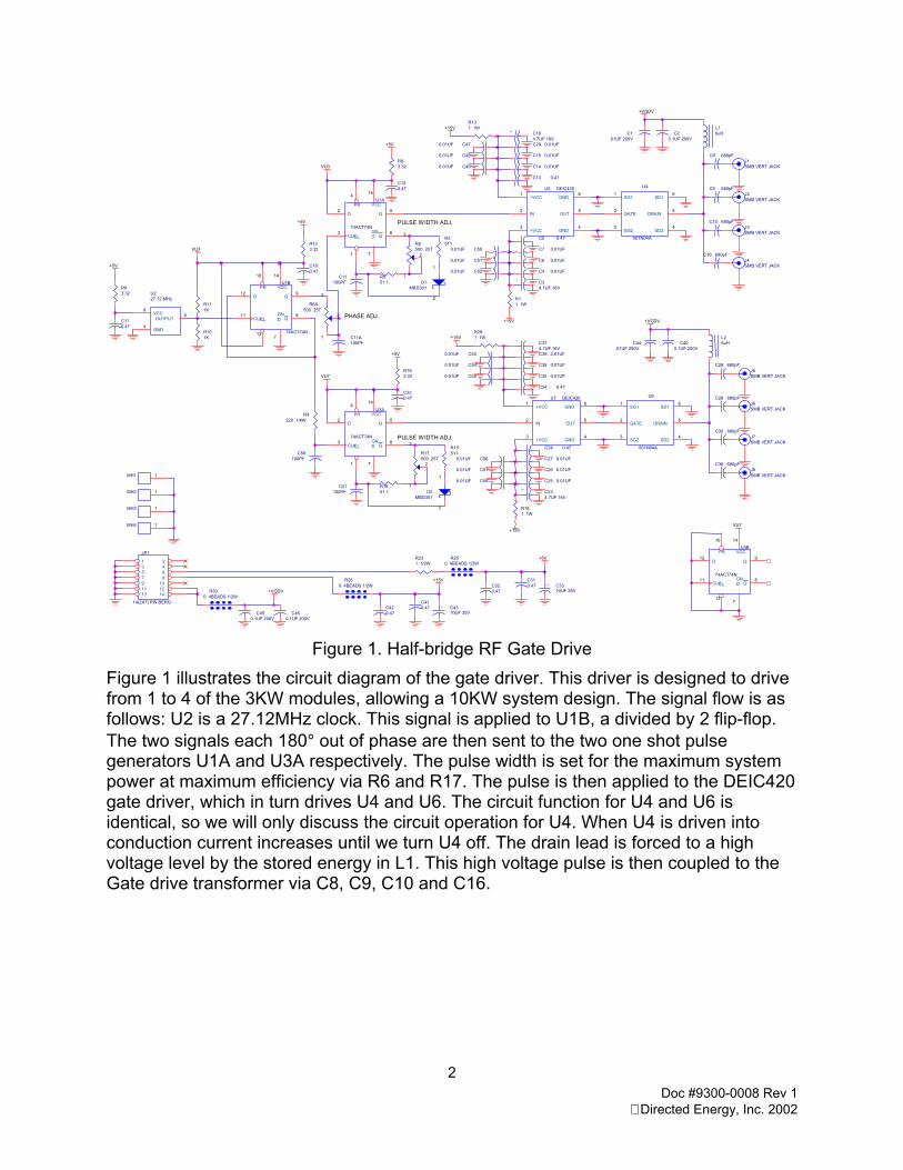
Figure 1. Half-bridge RF Gate Drive
Figure 1 illustrates the circuit diagram of the gate driver. This driver is designed to drive from 1 to 4 of the 3KW modules, allowing a 10KW system design. The signal flow is as follows: U2 is a 27.12MHz clock. This signal is applied to U1B, a divided by 2 flip-flop. The two signals each 180° out of phase are then sent to the two one shot pulse generators U1A and U3A respectively. The pulse width is set for the maximum system power at maximum efficiency via R6 and R17. The pulse is then applied to the DEIC420 gate driver, which in turn drives U4 and U6. The circuit function for U4 and U6 is identical, so we will only discuss the circuit operation for U4. When U4 is driven into conduction current increases until we turn U4 off. The drain lead is forced to a high voltage level by the stored energy in L1. This high voltage pulse is then coupled to the Gate drive transformer via C8, C9, C10 and C16.

3 Doc #9300-0008 Rev 1
Directed Energy, Inc. 2002
Figure 2 Gate Drive Module
Figure 2 illustrates the complete gate driver module. The primary gate driver outputs, on SMB connectors, are shown in the lower portion of the photograph. The power devices (DEIC420 Gate Drive ICs and DE150-501N04A MOSFETS) are mounted on the bottom side of the PCB.
Figure 3 Primary Gate Drives
The primary gate drives are illustrated in Figure 3. The voltage peaks at the drain of U4 are 300V. The high voltage power requirement for the gate drive module is approximately 61VDC @ ≈ .8A, 15V @ ≈3A and 5v @ < .1A. The 61V supply will vary in power consumption according to how many modules are being driven and what size output devices are chosen.
4 Doc #9300-0008 Rev 1
Directed Energy, Inc. 2002
HALF BRIDGE (DEI Module #5040-0290C)
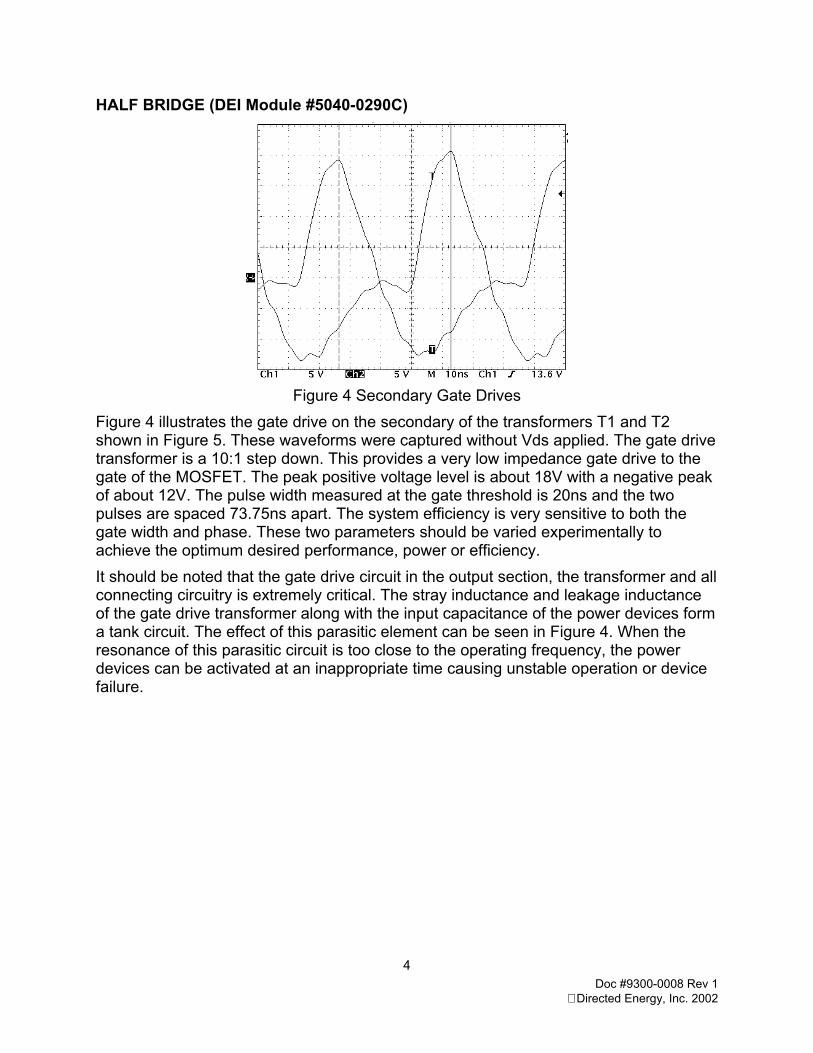
Figure 4 Secondary Gate Drives
Figure 4 illustrates the gate drive on the secondary of the transformers T1 and T2 shown in Figure 5. These waveforms were captured without Vds applied. The gate drive transformer is a 10:1 step down. This provides a very low impedance gate drive to the gate of the MOSFET. The peak positive voltage level is about 18V with a negative peak of about 12V. The pulse width measured at the gate threshold is 20ns and the two pulses are spaced 73.75ns apart. The system efficiency is very sensitive to both the gate width and phase. These two parameters should be varied experimentally to achieve the optimum desired performance, power or efficiency. It should be noted that the gate drive circuit in the output section, the transformer and all connecting circuitry is extremely critical. The stray inductance and leakage inductance of the gate drive transformer along with the input capacitance of the power devices form a tank circuit. The effect of this parasitic element can be seen in Figure 4. When the resonance of this parasitic circuit is too close to the operating frequency, the power devices can be activated at an inappropriate time causing unstable operation or device failure.

5 Doc #9300-0008 Rev 1
Directed Energy, Inc. 2002
T1XXuH
1
2
4
35
C6.01
C12 .01 C11
.01 C13 .01 C9
.01C1.01
C18 .01
J1SMB
T2XXuH
1
2
4
35
E3 RF GROUND
1
L1
25uH
E5GND
1
C8.01
C14 .01
MH1 1
U1102N10A
1
2
3 4
5
6SG1
GATE
SG2 SD2
DRAIN
SD1
E4 +VDS
1
C5.01
J2SMB
MH3 1
C19 .01 C7
.01
E2 RF OUTPUT
1
MH2 1
MH4 1
C15 .01 C10
.01 C2.01
C17 .01 C3
.01
U2102N10A
1
2
3 4
5
6SG1
GATE
SG2 SD2
DRAIN
SD1
C16 .01
E1 RF GROUND
1
C4.01
Figure 5 RF Output Stage
Figure 5 illustrates the RF output stage of the 3KW generator. The gate drive pulse of 20ns is applied to J1 and J2. These two drive pulses are offset in time by 73.75ns. U1 and U2 are driven into conduction on alternate half cycles. The advantages of the half bridge class D topology are that it allows the maximum utilization of the device operating area and that the output node can only move between +VDS and ground, providing a robust output stage to over-voltage conditions. The mechanical layout for this circuit is illustrated in Figure 6.
Figure 6 Half Bridge
Figure 6 is the half bridge section. The RF choke is in the center with high voltage supply by-passing on the left. The drain bypassing capacitors are in a row to the right of the RF choke, with the balance to the left of the U1 reference designator. The power devices are two DE375-102N12A MOSFETs, and are mounted on the bottom side of the PCB. The bridge output node is labeled E2, with a system ground on either side, E1 and E3. The construction of the two gate drive transformers is mechanically simple but very

6 Doc #9300-0008 Rev 1
Directed Energy, Inc. 2002
critical. It is important that the stray and leakage inductance be minimized as much as practical.
Figure 7 3KW Half-bridge Output
The voltage output of the half-bridge is illustrated in Figure 7. Here we see an 800V peak drain waveform on a 1KV device. This point is the node labeled RF OUTPUT in Figure 5. The shape and symmetry is very classical half-bridge performance. The high frequency oscillations on the flat-top and bottom of the waveform are the self-resonance of the output node capacitance and the loop inductance of the switch circuit. The frequency is approximately 200MHz for both the top half of the bridge and the lower half. From Figure 6 and Figure 7 we see that the half-bridge structure has a relatively low loop inductance, this is along with symmetry an important feature.
OUTPUT NETWORK
C316-101pF
C4275pF
C2 5-55pF
J1 RF JACK
C1 25pF
L12.1uH
1 2
E1 RF GROUND
1
E2 BRIDGE INPUT 1
Figure 8 3KW RF Tank and Load Matching
Figure 8 illustrates the output tank circuit. This tank is designed as a series resonant circuit at the fundamental operating frequency. Its role is four-fold. The series capacitor (C1 & C2) provides a DC block to prevent DC from flowing in the load, to provide a low-impedance path at the operating frequency fo, to reject harmonic current flow, and to convert the totem pole unipolar pulse to a sinusoidal output voltage. The Q of the resonant tank defines the circuit operating bandwidth as well as the tank peak voltages and losses. The loaded Q of the series tank in this configuration is approximately 10.
7 Doc #9300-0008 Rev 1
Directed Energy, Inc. 2002
In addition, an L-match section comprised of a portion of the series L (L1) and shunt C (C3 & C4) is used to match the totem-pole pair to the 50Ω output at J1. The tank was implemented using a combination of air variable capacitors and several “doorknob” style fixed value ceramic capacitors in parallel. Several capacitors were used to allow current sharing and to minimize capacitor ESR losses. Inductor L1 is air-wound built with 9T of ¼ inch OD copper tubing with a diameter of 2¼ inches and a length of 4 inches. The tank was tuned for the best compromise of Po and efficiency for a given buss voltage. For the 3kW operating point shown in Figure 8, the load presented to the bridge output is approximately 14+j12.6 Ω. For best output power efficiency a small inductive term is needed in the half bridge at the node labeled RF output in Figure 5 and BRIDGE INPUT in Figure 8. The stored energy in this inductive element forces the drain to ground or the +VDS supply during switch commutation dead time. This energy is used to charge or discharge the output capacitances at the bridge output node and allows the power stage to operate at high efficiencies. This effect can be seen on the bridge output waveform in Figure 7 as a slight discontinuity on the leading and trailing slopes.
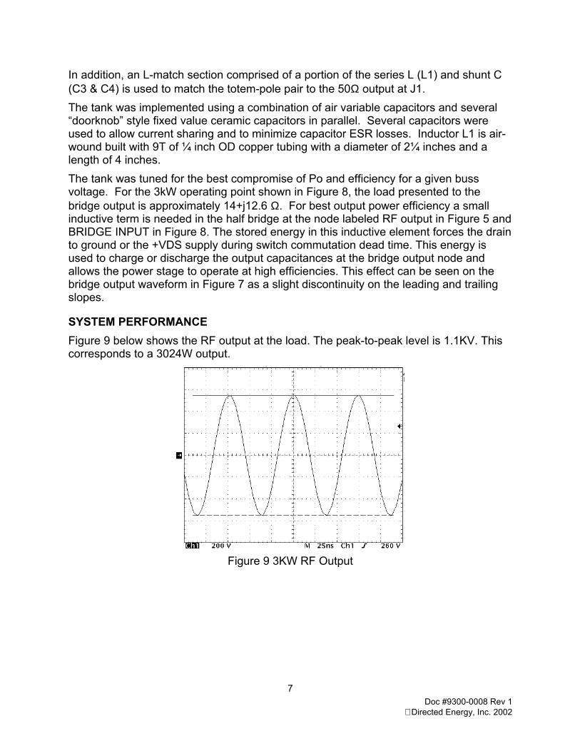
SYSTEM PERFORMANCE Figure 9 below shows the RF output at the load. The peak-to-peak level is 1.1KV. This corresponds to a 3024W output.
Figure 9 3KW RF Output

8 Doc #9300-0008 Rev 1
Directed Energy, Inc. 2002
Figure 10 illustrates the output spectrum of the tank circuit in Figure 8. The 3rd harmonic is down by –55db as shown. This represents a third harmonic output power of 9.5mW. This is a direct result of the medium Q tank circuit and its harmonic suppression capability.
Figure 10 RF Spectrum
Table 1 shows the operating parameters from 250W to 3KW in 250W increments. The RF power measurements were made using a Giga-Tronics 8651A power meter.
Table 1 3KW Operating Parameters
Po W Vin V Iin A Pin W VdsPk V Eff. % Ploss W 250 221 1.59 351.4 260 71.1 101.4
500 314 2.01 631.1 340 79.2 131.1
750 387 2.35 909.4 412 82.5 159.4
1000 450 2.66 1197 480 83.5 197
1250 501 2.93 1467.9 534 85.1 217.9
1500 552 3.19 1760 588 85.2 260
1750 597 3.42 2042 636 85.7 291.7
2000 640 3.65 2336 680 85.6 336
2250 682 3.87 2639 712 85.2 389
2500 722 4.09 2953 756 84.7 453
2750 762 4.29 3269 792 84.1 519
3000 800 4.49 3592 828 83.5 592
The DE375-102N12A power MOSFET has maximum ratings of VBds=1KV, Idm=12A and a maximum usable power dissipation of 550W. Given these three parameters and

9 Doc #9300-0008 Rev 1
Directed Energy, Inc. 2002
the chart above, it is clear that at 1000W and 2000W, the power levels are very conservative for the design. For a 1000W design we see from Table 1 above that the generator has substantial margin. The drain is operating at 50% of maximum; the current at 22% of maximum, and the power loss is 18% of maximum into a 50 Ohm load. For a 2000W design the drain voltage is at 68% of maximum, the drain current is at 32% of maximum, and the power loss is at 30% of maximum into a 50 Ohm load. Even at the 3000W level the drain is at 75%, the current at 37% and the power loss at 54% maximum. This is somewhat less conservative than the 1KW and the 2KW, however the margins are still significant.
3kW FREQUENCY AGILITY The 3kW module as originally designed is a relatively narrow band design, on the order of ±1% of f0. The driver stage as shown in Figure 1 is a narrowband design, tuned for optimum operation at the fundamental frequency of f0. During the tuning process the drain voltage for U4 and U6 was adjusted so that a 15Vp was applied to the Gates of the totem-pole pairs U1 and U2 shown in Figure 5. In addition, the value of coupling caps C8-C10, C16, C28-C30, and C36 were adjusted for best pulse shape at the gates of U1 and U2. Finally, the length of the coax cables interfacing between the driver and RF modules was adjusted for optimum wave shape at U1 and U2. The output tank as originally implemented (Figure 8), is a narrowband, medium Q design. Therefore the tuning was extremely sharp in response and the ability to vary the operating frequency was limited. If the frequency were varied even slightly lower in frequency, the final transistors in the half-bridge would fail due to hard switching. As the frequency increased, the module would produce power but the efficiency dropped off rapidly. Experiments were conducted to test the viability of adjusting the frequency about a center frequency f0. The goal was 13.56MHz ±10%. To achieve this goal the issues listed above needed to be addressed. The amplitude of the flyback driver stage varies with the drive frequency. As the frequency decreases the magnitude of the flyback output increases. This is a result of the L/C network interfacing between the driver and power modules. To achieve agility in frequency and maintain the applied Vgs to the Totem Pole MOSFETS U1 and U2, it was found that the magnitude of the “flyback” voltage, VGDV, needed to be adjusted. While testing for a given frequency, the voltage VGDV was adjusted for 14Vp at U1 and U2’s gates. Finally, a wideband, low Q, lumped element transformation was used to match the Totem Pole output to 50Ω. The 5kW combiner (Figure 15) was used. Initial design was done to ensure that an inductive load was presented to the totem pole outputs over the whole operating frequency range. The designed range was from 9+j10 to 16+j10 over 13.56MHz ±10%.
10 Doc #9300-0008 Rev 1
Directed Energy, Inc. 2002
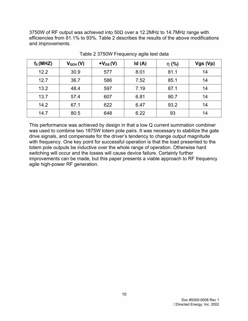
3750W of RF output was achieved into 50Ω over a 12.2MHz to 14.7MHz range with efficiencies from 81.1% to 93%. Table 2 describes the results of the above modifications and improvements.
Table 2 3750W Frequency agile test data
f0 (MHZ) VGDV (V) +VDS (V) Id (A) η (%) Vgs (Vp)
12.2 30.9 577 8.01 81.1 14
12.7 36.7 586 7.52 85.1 14
13.2 48.4 597 7.19 87.1 14
13.7 57.4 607 6.81 90.7 14
14.2 67.1 622 6.47 93.2 14
14.7 80.5 648 6.22 93 14
This performance was achieved by design in that a low Q current summation combiner was used to combine two 1875W totem pole pairs. It was necessary to stabilize the gate drive signals, and compensate for the driver’s tendency to change output magnitude with frequency. One key point for successful operation is that the load presented to the totem pole outputs be inductive over the whole range of operation. Otherwise hard switching will occur and the losses will cause device failure. Certainly further improvements can be made, but this paper presents a viable approach to RF frequency agile high-power RF generation.

11 Doc #9300-0008 Rev 1
Directed Energy, Inc. 2002
3KW SPICE MODEL The Spice model for the half bridge is show in Figure 11 below. The gate drive is applied to the primary of TX1 and TX2. These transformers are tightly coupled low stray capacitance and inductance devices. Their leakage reactance and ESR is modeled by L2, R7 and L5, R13. The switching circuit loop inductance is modeled by L3 and L6. The ESR of the bypass capacitors C3 and C4 are the resistors R3 and R5. The series resonant tank circuit is comprised of C5, C6, L4 and C7, C8.
Figure 11 Half Bridge Spice Model
Several output waveforms of this model are illustrated in the following figures.
12 Doc #9300-0008 Rev 1
Directed Energy, Inc. 2002
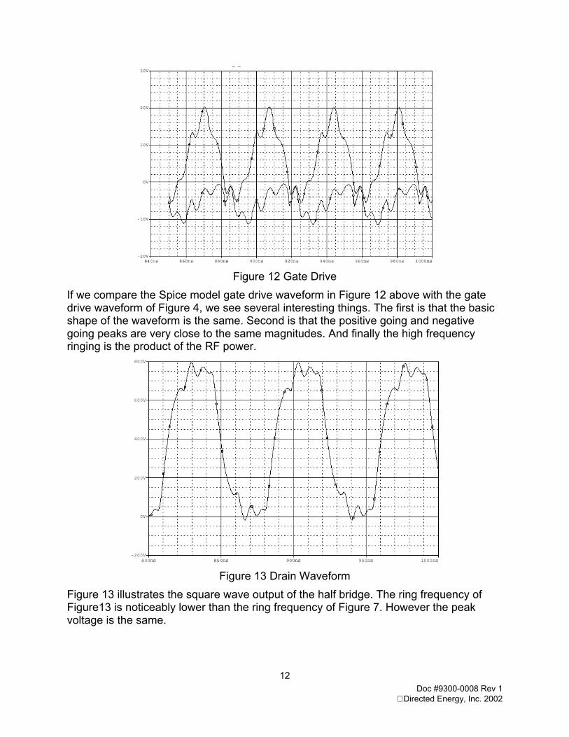
Figure 12 Gate Drive
If we compare the Spice model gate drive waveform in Figure 12 above with the gate drive waveform of Figure 4, we see several interesting things. The first is that the basic shape of the waveform is the same. Second is that the positive going and negative going peaks are very close to the same magnitudes. And finally the high frequency ringing is the product of the RF power.
Figure 13 Drain Waveform
Figure 13 illustrates the square wave output of the half bridge. The ring frequency of Figure13 is noticeably lower than the ring frequency of Figure 7. However the peak voltage is the same.

13 Doc #9300-0008 Rev 1
Directed Energy, Inc. 2002
Figure 14 RF Output
The RF output is illustrated in Figure 14. The peak-to-peak values of Figure 9 and this Figure are in agreement.
Table 3 3KW Spice Data
Po W Vin V Iin A Pin W VdsPkV Eff % Ploss W 240 221 1.4 309 224 80.8 69
480 314 1.9 597 315 82.1 117
979 450 2.7 1215 450 81.1 236
1466 552 3.3 1822 552 82.3 356
1989 640 3.8 2432 640 82.2 443
2530 722 4.2 3032 720 83.4 502
3124 800 4.8 3840 795 81.4 716
Table 3 above is the Spice output data. When we compare this table with the data in Table 1 we see a very good line-by-line correspondence. Having completed the 3KW half bridge, the next logical step is to combine two modules from the preceding section to provide a 5KW system. The combiner that was used for this development is shown below in Figure 15.

14 Doc #9300-0008 Rev 1
Directed Energy, Inc. 2002
Equivalent inputs from two half-bridge modules are shown as RF input A and RF input B. C1 and C4 block DC from the load while allowing the fundamental current at fo to flow with minimum loss. ATC 100E porcelain RF capacitors have an ESR ≤7mΩ each at 13.56MHz. As currents can approach 15Arms, these caps were chosen with absolute minimum ESR in mind. Inductors L1 and L2 are air-wound coils using 10 AWG magnet wire. The 4:1 output transformer is built using eight balun “Fair Rite” cores wound with two teflon RG-142 coaxes in parallel. The 50Ω output coaxial cable is RG-393. The combiner in Figure 15 functions by summation of equivalent currents in a low Q, resonant “T” match circuit. If each input waveform at RF INPUT A and B is identical, then identical currents flow through L1 and L2. Assuming twice the current, you can then replace L1 and L2 with a single inductor with ½ the inductance. Given this process and assuming a transformer leakage inductance of 175nH, each totem pole pair output load is approximately 12+j3Ω. As with the single 3kW single totem pole stage discussed earlier, for best output power efficiency, a small inductive term is required at each node labeled RF Input in Figure 15. The stored energy in this inductive element forces the drain to ground or to the +VDS supply during switch commutation dead time. This energy is used to charge or discharge the output capacitances at the bridge output node and allows the power stage to operate at high efficiencies.
L1 384nHC1 5100pF X2
L2 384nHC4 5100pF X2
C2100pF X6 7.2KV
C360pF 7.2KV
RF INPUT A
RF INPUT B
RF TRANSFORMER1:4 RF OUTPUT to 50 OHMS
Figure 15 5KW Combiner
15 Doc #9300-0008 Rev 1
Directed Energy, Inc. 2002
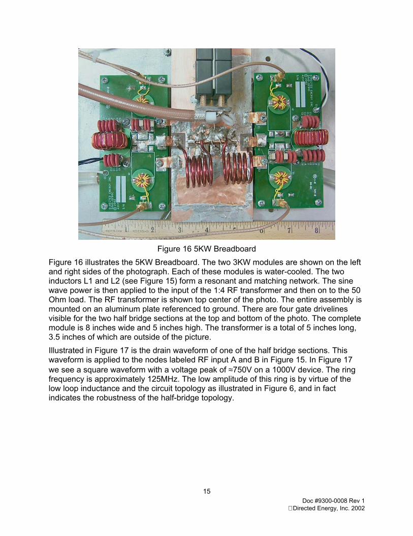
Figure 16 5KW Breadboard
Figure 16 illustrates the 5KW Breadboard. The two 3KW modules are shown on the left and right sides of the photograph. Each of these modules is water-cooled. The two inductors L1 and L2 (see Figure 15) form a resonant and matching network. The sine wave power is then applied to the input of the 1:4 RF transformer and then on to the 50 Ohm load. The RF transformer is shown top center of the photo. The entire assembly is mounted on an aluminum plate referenced to ground. There are four gate drivelines visible for the two half bridge sections at the top and bottom of the photo. The complete module is 8 inches wide and 5 inches high. The transformer is a total of 5 inches long, 3.5 inches of which are outside of the picture. Illustrated in Figure 17 is the drain waveform of one of the half bridge sections. This waveform is applied to the nodes labeled RF input A and B in Figure 15. In Figure 17 we see a square waveform with a voltage peak of ≈750V on a 1000V device. The ring frequency is approximately 125MHz. The low amplitude of this ring is by virtue of the low loop inductance and the circuit topology as illustrated in Figure 6, and in fact indicates the robustness of the half-bridge topology.

16 Doc #9300-0008 Rev 1
Directed Energy, Inc. 2002
Figure 17. 5KW Drain Voltage Waveform
Figure 18 5KW RF OUTPUT
The RF output shown in Figure 18 is a peak-to-peak value of 1480V into 50 Ohms. This yields an output power of 5474 Watts. The data in Table 3 were taken with a Bird model 43 Wattmeter.
17 Doc #9300-0008 Rev 1
Directed Energy, Inc. 2002
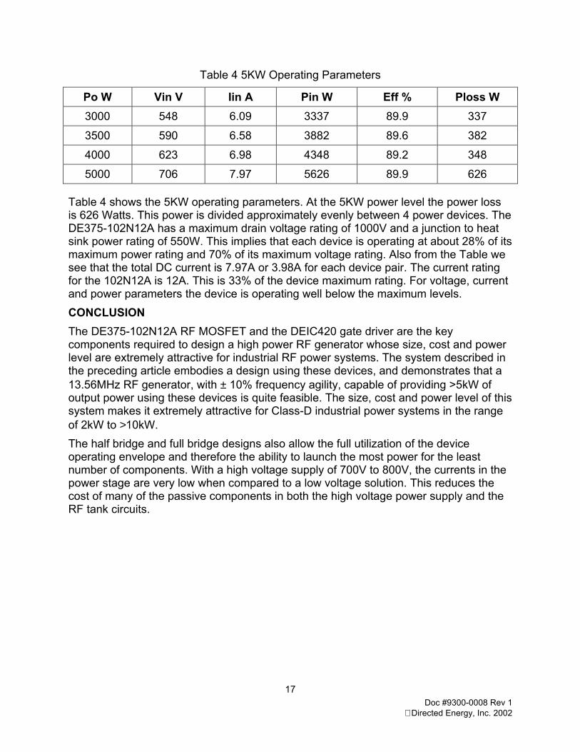
Table 4 5KW Operating Parameters
Po W Vin V Iin A Pin W Eff % Ploss W 3000 548 6.09 3337 89.9 337
3500 590 6.58 3882 89.6 382
4000 623 6.98 4348 89.2 348
5000 706 7.97 5626 89.9 626
Table 4 shows the 5KW operating parameters. At the 5KW power level the power loss is 626 Watts. This power is divided approximately evenly between 4 power devices. The DE375-102N12A has a maximum drain voltage rating of 1000V and a junction to heat sink power rating of 550W. This implies that each device is operating at about 28% of its maximum power rating and 70% of its maximum voltage rating. Also from the Table we see that the total DC current is 7.97A or 3.98A for each device pair. The current rating for the 102N12A is 12A. This is 33% of the device maximum rating. For voltage, current and power parameters the device is operating well below the maximum levels. CONCLUSION The DE375-102N12A RF MOSFET and the DEIC420 gate driver are the key components required to design a high power RF generator whose size, cost and power level are extremely attractive for industrial RF power systems. The system described in the preceding article embodies a design using these devices, and demonstrates that a 13.56MHz RF generator, with ± 10% frequency agility, capable of providing >5kW of output power using these devices is quite feasible. The size, cost and power level of this system makes it extremely attractive for Class-D industrial power systems in the range of 2kW to >10kW. The half bridge and full bridge designs also allow the full utilization of the device operating envelope and therefore the ability to launch the most power for the least number of components. With a high voltage supply of 700V to 800V, the currents in the power stage are very low when compared to a low voltage solution. This reduces the cost of many of the passive components in both the high voltage power supply and the RF tank circuits.

18 Doc #9300-0008 Rev 1
Directed Energy, Inc. 2002
REFERENCES
1. Herbert L. Krauss and Charles W. Bostian Solid State Radio Engineering Copyrighted 1980, John Wiley & Sons ISBN 0-471-03018-X
2. Mihai Albulet RF POWER AMPLIFIERS Copyrighted 2001, Noble Publishing ISBN 1-884932-12-6