3d stacked memory: patent landscape analysis - wipo · page | 2 3d stacked memory: patent landscape...
TRANSCRIPT

3D Stacked Memory: Patent Landscape Analysis

3D Stacked Memory: Patent Landscape Analysis
Table of Contents
Executive Summary……………………………………………………………………….…………………….1
Introduction…………………………………………………………………………….…………………………..2
Filing Trend………………………………………………………………………………….……………………….7
Taxonomy…………………………………………………………………………………….…..……….…………8
Top Assignees……………………………………………………………………………….….…..……………11
Geographical Heat Map…………………………………………………………………….……………….13
LexScoreTM…………………………………………………………….…………………………..….……………14
Patent Strength……………………………………………………………………………………..….……….16
Licensing Heat Map………………………………………………………….…………………….………….17
Appendix: Definitions………………………………………………………………………………….……..19
Page | 1 3D Stacked Memory: Patent Landscape Analysis
EXECUTIVE SUMMARY
Memory bandwidth, latency and capacity have become a major performance bottleneck as more and
more performance and storage are getting integrated in computing devices, demanding more data
transfer between processor and system memory (Volatile and Non-Volatile). This memory bandwidth
and latency problem can be addressed by employing a 3D-stacked memory architecture which provides
a wide, high frequency memory-bus interface. 3D stacking enables stacking of volatile memory like
DRAM directly on top of a microprocessor, thereby significantly reducing transmission delay between
the two. The 3D- stacked memory also improves memory capacity and cost of non-volatile storage
memory like flash or solid state drives. By stacking, memory dies vertically in a three-dimensional
structure, new potential for 3D memory capacities are created, eliminating performance and reliability
issues from capacity limitations.
In this report, we study the Intellectual Property (Patents) landscape of this fast growing technology. We
find that the majority of patenting activity has occurred in technologies related to wafer manufacturing
processes step BEOL and FEOL with impact on design parameters such as, ‘Structural Features’, ‘Model
Parameters’, ‘Operating Speed’. We also find that majority of the patents/patent applications are
distributed among top three companies. The share of these top three assignees is around 52% of the
total patents/patent applications (considered for analysis) in this technology domain. SanDisk is at the
top and holds around 34% of the total patents followed by Micron and Samsung. The US geography has
seen the maximum patent filings and, is followed by the other big markets such as China, Japan, South
Korea and Taiwan.
Using our proprietary patent analytics tool, LexScoreTM, we identify SanDisk as the leader in this
technology domain with good patent portfolio quality as well as quantity. Micron also holds a large
number of patents in this domain. The combination of patent holding pattern and a high patent filing
activity suggest a significant potential for patent licensing activity in this technology domain. Using our
proprietary Licensing Heat-map framework, we predict 3D memory stacking technology sub domains for
licensing activity.
The top assignee, SanDisk shares a fabrication plant with Toshiba which also appears among the top
seven assignees in this technology. Samsung is working on its own 3D stacked memory and has released
several iterations till now. Several companies are entering into partnerships to use each other’s
resources. On the other hand, Guobiao Zhang is the individual inventor of 57 patents/patent
applications in 3D stacked memory technology. Micron Technology with its existing partnership with
Intel plans to release 10TB flash memory in a 2mm chip by the end of this year.
In the following sections, we present our analysis of the Patent Landscape of this technology domain.

Page | 2 3D Stacked Memory: Patent Landscape Analysis
INTRODUCTION
With the increased demand for enhanced functionality and miniaturization in
portable hand-held devices such as cell phones, digital cameras and laptops—
equipment manufacturers have focused on reducing the component footprint in
assembling these devices. Processors and storage memories (volatile and non-
volatile) are two most important ingredients in manufacturing computing
devices that determine form factor and functionality. The memory needs for
modern portable devices requires high capacity, low latency and compact form
factor. This requires not only innovative nanoscale memory cell designs but also
innovative packaging technologies to provide high capacity with compact size.
Silicon chip manufacturers have turned to 3D memory stacking solutions to
provide high capacity and smaller size. Stacking of multiple memory chips, not
only provides a reduction in overall package footprint, but also a significant
improvement in electrical performance due to shorter interconnects. This
facilitates quicker signal transmission (low data latency) requiring less energy to
drive the signals. This enables a new generation of tiny but powerful devices
with high storage capacity and performance.
The memory and processor always co-exist in a computing device. The
processor has controller that communicates with the memory. The memory and
processors are usually designed in different manufacturing process technology
nodes due to cost and performance advantages. If transistors get any smaller,
their reliability could become questionable and the cost of manufacturing in sub
28nm node is much higher. Such issues have led to the adoption of three-
dimensional (3D) integrated circuit manufacturing technology, where two or
more dice are stacked atop each other and linked with suitable interconnects.
The primary benefit is that the electrical interconnects between blocks are
shorter apart from compact size. This lowers power dissipation and operational
latency since fewer buffers, flip-flops and shorter transmission lines are needed.
Reducing the amount of metal that runs across the chip also reduces power
dissipation. Lower inter-block latency reduces cycle time, increases
responsiveness and chip performance. Stacking layers also increases chip
density, as more transistors are able to be placed per unit of volume and within
one clock cycle of each other.
There are three main ways of stacking chips; the first technique involves
stacking two chips together, and then connecting them through flip chip
bonding at the bottom of the stack. This technique can be used to place DRAM
on the top of a CPU. The second technique is called through-silicon via (TSV).
With TSV, vertical copper channels are built into each die, so that when they’re
placed on top of each other, the TSVs connect the chips together (as shown in
the figure). This is the technique that was initially developed by IBM. CMOS
image sensors were first to adopt TSV in high volume manufacturing. These
have seen resurgence due to need for compact size in smartphones, tablets and
IBM, École
Polytechnique
Fédérale de
Lausanne (EPFL)
and the Swiss
Federal Institute of
Technology Zurich
(ETH) signed a
four-year
collaborative
project called
CMOSAIC to
understand how
the latest chip
cooling techniques
can support a 3D
chip architecture.
Nvidia is using
what is called
Vertical stacking
3D, or on-package
stacked DRAM for
its Pascal 2016
GPUs.

Page | 3 3D Stacked Memory: Patent Landscape Analysis
laptops. TSV’s allow for stacking of volatile memory DRAM with processor
(memory controller) to build very compact devices for portable applications.
This technique also allows 3D stacking of memory chip to create dense non-
volatile memory like flash or solid state drives with high capacity.
Figure 1: 3D Memory Stack using TSV technique1
The third technique is advanced packaging method which uses a silicon
transposer. A transposer is effectively a piece of silicon that acts like a mini
motherboard, connecting two or more chips together. The advantage of this
technique is that you can have shorter wiring (higher bandwidth, lower power
consumption), but the constituent chips can be of different manufacturing
technology or type. Transposers are expected to be used in upcoming multi-
GPU Nvidia and AMD graphics cards.
The second technique called through-silicon-via (TSV) is most widely used for
stacking memory chips. This is essentially a wafer level packaging method where
a via goes from the front side of the wafer (typically connecting to one of the
lower metal layers) through and out to the back. TSVs vary in diameter from
1um to 10um, with a depth of 5 to 10 times the width. A hole is formed into the
wafer, lined with an insulator, and then filled with copper or tungsten. The
wafer is thinned to expose the backside of the TSVs. The wafer is thinned using
CMP (chemical mechanical polishing) until the TSVs are almost exposed. More
silicon is then etched away to reveal the TSVs themselves. FEOL (front-end of
line) in fab manufacturing is where transistors are created. BEOL (back-end of
line) is where interconnects between transistors are created. TSV’s can be
manufactured in three different ways. TSVfirst (build them before the
transistors/FEOL) and TSVlast (build them after BEOL). In TSVmiddle process,
the TSVs are formed between transistors and interconnects. TSV first is no
longer viable due to high via resistances. TSV last approach has been popular in
CMOS image sensors due to need for high aspect ratio. This method is
1 Chip-to-Chip Input/Output (I/O) Thrust, Advanced Computing Systems Group
ThruChip
Communications'
ThruChip Interface
(TCI) utilizes
inductive curls
that impart layer-
to-layer as
opposed to the
physical metal
wires utilized by
through-silicon by
means of (TSV)
tech to connection
a 3D chip's silicon
layers.
Toshiba and
SanDisk announce
BiCS as the first
48-layer 3D flash
chip.

Page | 4 3D Stacked Memory: Patent Landscape Analysis
challenging for high-density 3D IC applications. TSVmiddle is more commercially
viable and popular method for 3D stacking of integrated circuits. In this method
after interconnects creation the micro bumps are created. The wafer is glued to
a glass carrier. The back is then grinded down and a passivation layer is applied.
This is then etched to expose the TSVs and then micropads are created. The
figure below shows the TSVmiddle approach of manufacturing flow.
Figure 2: 3D TSV process flow2
The growing importance of 3D stacking in industry has led to an extensive
research in this area. Applied Materials (manufacturing equipment maker for
Intel, TSMC, Samsung, Global Foundries, and other foundries) and A*STAR's
Institute of Microelectronics (IME) have declared the opening of a forefront 3D
chip bundling lab in Singapore. Assembled with a consolidated speculation of
over $100 million, the Center of Excellence in Advanced Packaging highlights a
14,000 square foot cleanroom containing a finish 300-millimeter creation line
and 3D bundling instruments that are novel to A*STAR.
In 2004, Intel3 presented a 3D version of the Pentium 4 CPU. The chip was
manufactured with two dice using face-to-face stacking, which allowed a dense
via structure. Backside TSVs were used for I/O and power supply. For the 3D
floor-plan, designers manually arranged functional blocks in each die aiming for
power reduction and performance improvement. Splitting of large and high-
power blocks and careful rearrangement limited thermal hotspots. The 3D
2 TSV MEOL Process Flow for Mobile 3D IC Stacking, 3dincites.com, August 7, 2014 3 Generations of the computer processors, Piotr Gwizdała
TSVs are utilized,
for instance, in
Micron's Hybrid
Memory Cube
(HMC) and
Samsung's
vertically stacked
NAND (V-NAND)
chips, and are
under
concentrated study
by various chip
creators and
fabricators.
The worldwide 3D
IC market is
expected to
develop from $2.21
billion in 2009 to
$6.55 billion in
2015 at a CAGR of
16.9% from 2011
to 2015.

Page | 5 3D Stacked Memory: Patent Landscape Analysis
design provided 15% performance improvement (due to eliminated pipeline
stages) and 15% power saving (due to eliminated repeaters and reduced wiring)
as compared to the 2D Pentium 4.
The Teraflops Research Chip4, introduced in 2007 by Intel was an experimental
80-core design with stacked memory. Due to the high demand for memory
bandwidth, a traditional I/O approach would consume 10 to 25 W. To improve
upon that, Intel designers implemented a TSV-based memory bus. Each core is
connected to one memory tile in the SRAM die with a link that provides 12 GB/s
bandwidth, resulting in a total bandwidth of 1 TB/s while consuming only 2.2 W.
As market players compete to realize the huge economic potential offered by
the 3D stacking, we have seen M&A, partnerships and product announcements
in 3D memory stacking technology domain. Intel and its partner Micron
announced 3D NAND solution that enables chips with 384Gbit (48GB) of
capacity which is three times to that of existing 3D NAND parts. Along with
higher densities, Intel/Micron promise lower costs, improved read/write
performance, and new sleep modes that cut power to inactive parts of a chip.
The offerings take aim at Samsung, which has been shipping 3D NAND memory
parts for several months, as well as Toshiba and its partner SanDisk. AMD has
reported that it would be mutually working with memory device manufacturer,
SK Hynix, in the development of cutting edge High-bandwidth 3D stacked
memory items and arrangements.
SanDisk's recent profit5 warning shows potential headwinds in the NAND Flash
memory space, which represents to 28% of Micron's income. Samsung's new
$14.7B chip production line has a high probability of upsetting the fragile
supply-demand balance in the DRAM business, which represents 68% of
Micron's income.
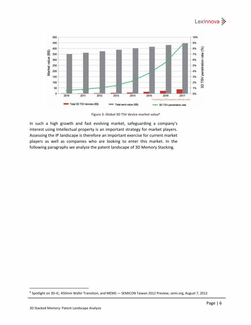
The worldwide 3D IC market is expected to grow from $2.21 billion in 2011 to
$6.55 billion in 2015 at a CAGR of 16.9% from 2011 to 2015. The organizations in
this business need to productively adjust their expenditure between capacity
extension and research & development. This is viewed as critical for subsequent
sustainability and growth for 3D ICs business. This balance is driven by
penetration of 3D-stached memory into computing devices. Following figure
shows this.
4 Intel Details 80-Core Teraflops Research Chip, xbitlabs.com, Anton Shilov, February 12, 2007 5 Micron: This Time Is Not Different, Seeking Alpha, January 16, 2015
Intel and its
partner Micron,
announced 3D
NAND solution that
enables chips with
384Gbit (48GB) of
capacity which is
three times to that
of existing 3D
NAND parts. AMD has reported
that it would be
mutually working
with memory
device
manufacturer, SK
Hynix, in the
development of
cutting edge High-
bandwidth 3D
stacked memory
items and
arrangements.
Page | 6 3D Stacked Memory: Patent Landscape Analysis
Figure 3: Global 3D TSV device market value6
In such a high growth and fast evolving market, safeguarding a company’s
interest using Intellectual property is an important strategy for market players.
Assessing the IP landscape is therefore an important exercise for current market
players as well as companies who are looking to enter this market. In the
following paragraphs we analyze the patent landscape of 3D Memory Stacking.
6 Spotlight on 3D-IC, 450mm Wafer Transition, and MEMS — SEMICON Taiwan 2012 Preview, semi.org, August 7, 2012

Page | 7 3D Stacked Memory: Patent Landscape Analysis
Filing Trend
Figure below shows the number of patent/patents applications related to 3D
stacked memory between 1995 and 2014. The IP activity has seen steady
increase from 1995 to 2005 with a sharp rise in 2006. The patent activity nearly
doubled from 99 in 2005 to 198 in 2006. In 2006, SanDisk increased its IP filing
actively in this domain which resulted in the spike. The filing activity tapered off
between 2006 and 2010 due to economic downturn but picked off post-
recession, increasing from 175 in 2010 to 283 in 2012. The 2013 & 2014 trends
show lower number because the full published data is not available till now and
the numbers are incomplete. This does not imply that patent filings in 2013 &
2014 have actually gone down.
Figure 4: Filing Trend
0
50
100
150
200
250
300
19
95
19
96
19
97
19
98
19
99
20
00
20
01
20
02
20
03
20
04
20
05
20
06
20
07
20
08
20
09
20
10
20
11
20
12
20
13
20
14
In 2004, Tezzaron
Semiconductor
built working 3D
devices from six
different designs.
The chips were
built in two layers
with "via-first"
tungsten TSVs for
vertical
interconnection.

Page | 8 3D Stacked Memory: Patent Landscape Analysis
Taxonomy
3D memory stacking technology exploits the third or Z height dimension to
provide a volumetric packaging solution for higher integration and performance.
3D stacking has become critical for enhancing the multi-media features
consumers demand in smaller, lighter products. This increasing functionality
requires higher memory capacity in more compact size. New product designs
(cell phones, digital cameras, PDAs, audio players and mobile gaming) demand
diverse feature set in innovative form factor and styling. 3D stacking enables
these designs with highest level of device integration, area efficiency at a low
cost. The taxonomy is presented in the form of a 2D matrix with manufacturing
processes on one axis and design parameters on the other. The taxonomy
focuses on the impact of various manufacturing processes on the design
parameters. The categorization of patents/patent applications, related to 3D
memory stacking was done on the basis of manufacturing processes and the
affected design parameters. The set considered for the analysis comprised of
around 2,300 patents/patent applications.
The manufacturing process is divided into FEOL (Front-end-of-line), BEOL (Back-
end-of-line), Assembly and Testing. 3D stacked memory technology impacts
BEOL & FEOL manufacturing the most as most building happens there. Most
patents/patent applications fall in BEOL & FEOL manufacturing process. Due to
this, FEOL is further divided into processes involved in the manufacturing of
devices, such as Wafer Development, Oxide Growth, Lithography, Etching,
Device Formation, Stacking and Others. Also, BEOL is further divided into
processes involved in the manufacturing of devices, such as Metal Layer
Formation, Interconnects Formation, Contact Formation, and Others.
The design parameters are classified as Structural features, Design Flow, Model
Parameters, Power Consumption, Feature Size, Operating Voltage, Operating
Speed and leakage current.
Please refer to Appendix for detailed definitions of the various categories.
Stanford
engineers have
build 3D “high-
rise” chips that
could leapfrog the
performance of
the single-story
logic and memory
chips on today’s
circuit cards,
which are subject
to frequent traffic
jams between
logic and memory.

Page | 9 3D Stacked Memory: Patent Landscape Analysis
Figure 5: Taxonomy
In the manufacturing processes category, FEOL and BEOL are of interest. There
are 1468 patents/patent applications in FEOL, and 1549 in BEOL. In FEOL
category, the following sub-domains are of interest: Stacking, Etching and
Device Formation. There are 899 patents/patent applications in ‘Stacking’, 395
in ‘Etching’, and 322 in ‘Device Formation’. There are some patents/patent
applications that cover multiple manufacturing processes and multiple design
parameters.
In the design parameters category, the following sub-domains are of interest:
Structural Features, Model Parameters, Operating Voltage, and Operating
Speed. There are 1743 patents/patent applications in ‘Structural features’, 523
in ‘Model Parameters’, 357 in ‘Operating Voltage, and 311 in ‘Operating Speed’.
Stacking is an important step in the formation of 3D stacked memory. In this
process, the individual devices are stacked on the top of other devices and are
interconnected by metallic interconnects.
Etching is a critically important process in the manufacturing of a 3D memory
stack. Every wafer undergoes many etching steps before the manufacturing is
complete. Etching is used to chemically remove layers from the surface of a
wafer during fabrication. The part of the wafer is protected from the etchant by
a mask which resists etching.
Device Formation refers to the formation of gate, source and drain on the
substrate layer. Gate film is formed by oxidation and then, plasma nitridation
process is applied to the surface of the gate film. Gate electrode (polysilicon) is
formed on it by CVD (Chemical Vapor Deposition) method. The impurities
(specific elements) are diffused into the substrate by ion-implantation to form
source and drain.
Samsung has huge
arrangements for
future emphases
of the V-NAND
tech,
incorporating 3D
chips with up to
24 layers, all
associated by
utilizing "unique
carving
innovation" to
bore down
through the layers
and interface them
electronically.

Page | 10 3D Stacked Memory: Patent Landscape Analysis
Structural features refer to the structural components of devices. Since 3D stack
memory technology is functionally a passive interconnect structure so most of
the patents/patent applications fall under structural feature.
Model Parameters refer to electrical characteristics of 3D stack memory
technology. These parameters have a great impact on the performance of an
interconnect, is an important factor in 3D stack memory technology.
Operating voltage and Operating speed are important design parameters in 3D
stack memory technology . Operating Voltage is the minimum voltage required
for the proper operation of a device and Operating speed refers to the time
taken by a device to generate the output after an input is applied to it.
SanDisk's recent
profit warning
shows potential
headwinds in the
NAND Flash
memory space,
which represents
to 28% of Micron's
incomes.

Page | 11 3D Stacked Memory: Patent Landscape Analysis
Top Assignees
Figure below depicts the top assignees having patents/patent applications
related to 3D Stacked Memory Technology.
SanDisk, Micron and Samsung are the top three assignees with 793, 219 and 194
patents/patent applications respectively. The numbers of patents/patent
applications owned by top three assignees comprise around 52% of the total
patents/patent applications (around 2,300) filed in the domain which are
considered in the analysis. Guobiao Zhang is an individual inventor who has 57
patents/patent applications.
The top assignee, SanDisk shares a fabrication plant with Toshiba which also
appears among the top seven assignees in this technology. Samsung is working
on its own 3D stacked memory and has released several iterations till now.
Several companies are entering into partnerships to use each other’s resources.
On the other hand, Guobiao Zhang is the individual inventor of 57
patents/patent applications in 3D stacked memory technology. Micron
Technology, in partnership with Intel, is planning to release memory of 10TB
flash memory in a 2mm chip by the end of this year.
The R & D expenses of SanDisk in the last 3 years are US$ 602.8, US$ 742.3 and
US$ 852.3 million and that of Micron, US$ 918, US$ 931 and US$ 1,371 million
and that of Samsung, US$ 212.29, US$ 304.66 and US$ 327.73 million
respectively. This shows that R & D expenses of all the top assignees have
increased since last 3 years and are expected to increase more. Moreover, the
revenues of all the companies are also increasing. For Sandisk, revenues
increased from US$ 5052.5 to US$ 6,627.7 million between 2012 and 2014 and
for Micron, revenues increased from US$ 8,234 to US$ 16,358 million and for
Samsung, revenues decreased from US$ 7177.57 to US$ 6479.95 million
respectively.
Figure 6: Top Assignees
The Low Power
Memories
Subcommittee (JC-
42.6) has
published a
standard for Wide
I/O Mobile DRAM
with TSV
interconnects
stacked on System
on a Chip (SoC)
Application
Processors.

Page | 12 3D Stacked Memory: Patent Landscape Analysis
The maximum number of patents/patent applications filings has been done in the year 2006 and 2007
by SanDisk. The companies listed in following table can be termed as top leaders in terms of their patent
portfolio.
Table 1: Top Assignees year-wise trend

Page | 13 3D Stacked Memory: Patent Landscape Analysis
Geographical Heat Map
The United States has seen maximum number of patent filings in domain of 3D
stacked memory technology. China, Japan, Korea and Taiwan have also seen
good number of patent filings.
SanDisk is the top assignee with 793 patent/patents applications with 412 in the
United States. Samsung has 18 patent/patents applications in China where as an
individual inventor Guobiao Zhang has 16. The 3D memory patents/patent
applications are concentrated in traditional memory manufacturing countries
like US, China, Japan, Korea and Taiwan.
Figure 7: Geographical Heat Map
Toshiba is trying
to leapfrog
Samsung’s
maximum density
with 48-layer
memory, as
opposed to the
Korean
manufacturer’s
current 32-layer
designs.
Page | 14 3D Stacked Memory: Patent Landscape Analysis
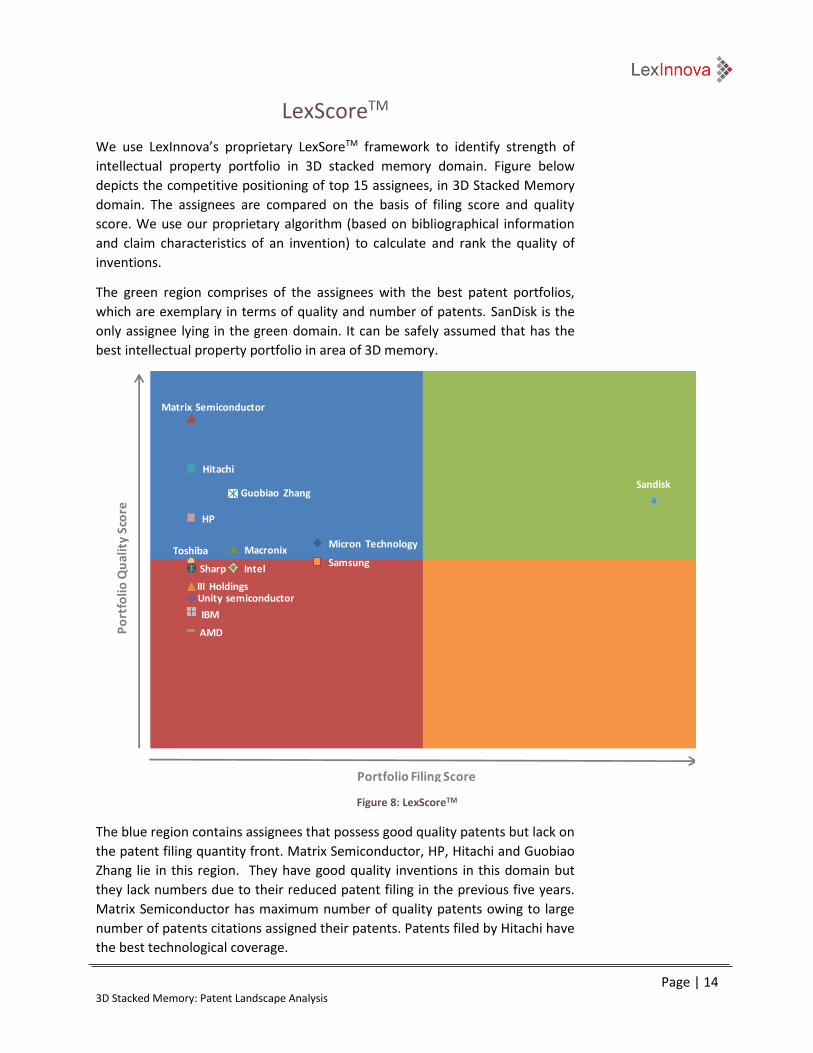
LexScoreTM
We use LexInnova’s proprietary LexSoreTM framework to identify strength of
intellectual property portfolio in 3D stacked memory domain. Figure below
depicts the competitive positioning of top 15 assignees, in 3D Stacked Memory
domain. The assignees are compared on the basis of filing score and quality
score. We use our proprietary algorithm (based on bibliographical information
and claim characteristics of an invention) to calculate and rank the quality of
inventions.
The green region comprises of the assignees with the best patent portfolios,
which are exemplary in terms of quality and number of patents. SanDisk is the
only assignee lying in the green domain. It can be safely assumed that has the
best intellectual property portfolio in area of 3D memory.
Figure 8: LexScoreTM
The blue region contains assignees that possess good quality patents but lack on
the patent filing quantity front. Matrix Semiconductor, HP, Hitachi and Guobiao
Zhang lie in this region. They have good quality inventions in this domain but
they lack numbers due to their reduced patent filing in the previous five years.
Matrix Semiconductor has maximum number of quality patents owing to large
number of patents citations assigned their patents. Patents filed by Hitachi have
the best technological coverage.
Micron Technology
SamsungMacronix
Intel
Guobiao Zhang
Toshiba
IBM
Matrix Semiconductor
AMD
Unity semiconductor
Hitachi
III Holdings
HP
Sharp
Sandisk
Portfolio Filing Score
Po
rtfo
lio
Qu
ali
ty S
core
Page | 15 3D Stacked Memory: Patent Landscape Analysis
Most of the assignees form a cluster in the red region with patent portfolio
lacking on both patent quality and quality of filing. IBM, Unity Semiconductor,
and AMD have filed most of their patents within past three years (2012-14);
hence the patents quality is hampered. Their patent portfolio may rise in future
after successful prosecution of their patents that are in pipeline and more
citations may get added. Patents assigned to III Holdings have the lowest
geographical score as they have filed their patents/patent applications only in
the USA.
Page | 16 3D Stacked Memory: Patent Landscape Analysis
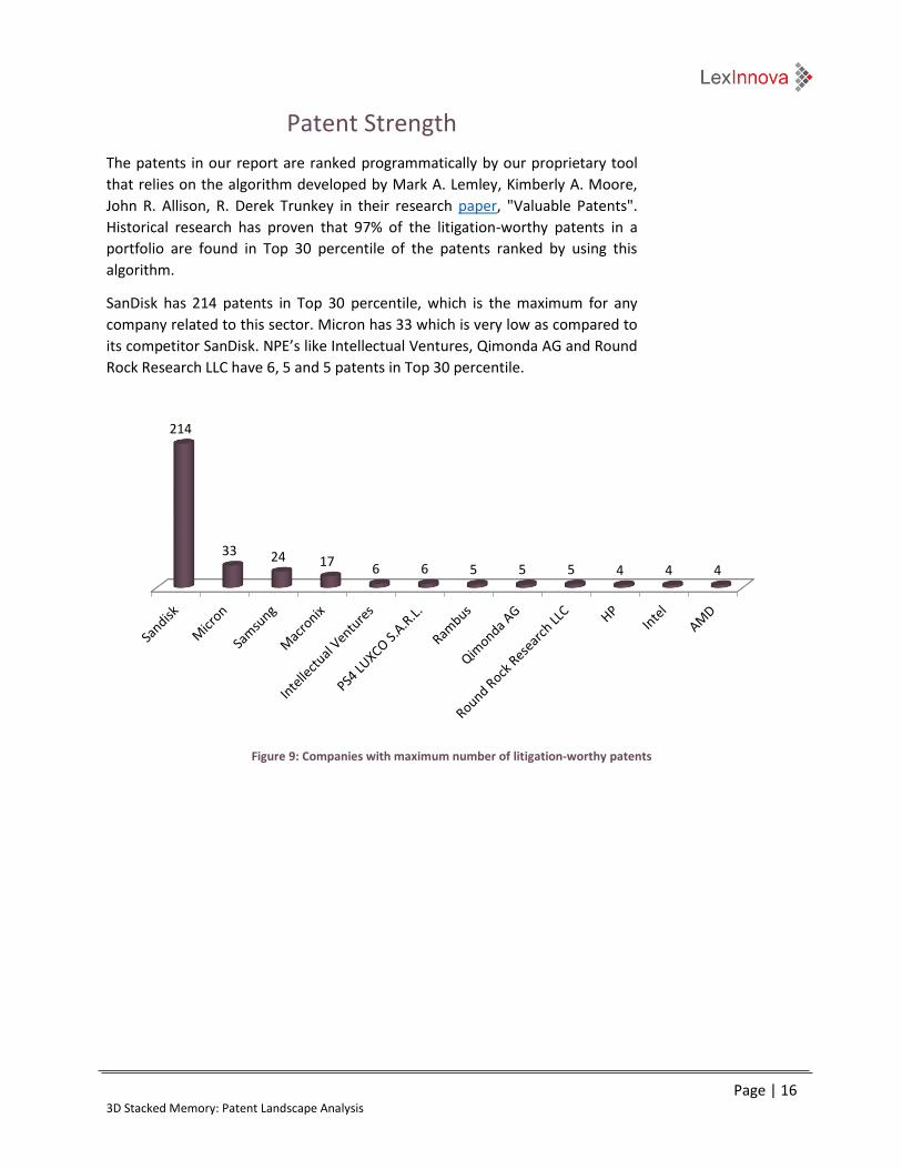
Patent Strength
The patents in our report are ranked programmatically by our proprietary tool
that relies on the algorithm developed by Mark A. Lemley, Kimberly A. Moore,
John R. Allison, R. Derek Trunkey in their research paper, "Valuable Patents".
Historical research has proven that 97% of the litigation-worthy patents in a
portfolio are found in Top 30 percentile of the patents ranked by using this
algorithm.
SanDisk has 214 patents in Top 30 percentile, which is the maximum for any
company related to this sector. Micron has 33 which is very low as compared to
its competitor SanDisk. NPE’s like Intellectual Ventures, Qimonda AG and Round
Rock Research LLC have 6, 5 and 5 patents in Top 30 percentile.
Figure 9: Companies with maximum number of litigation-worthy patents
214
33 24 176 6 5 5 5 4 4 4

Page | 17 3D Stacked Memory: Patent Landscape Analysis
Licensing Heat Map
We use our LexInnova’s Licensing-Heat Map (Figure below) framework to
identify technology sub-domains in the field of 3D stacked memory technology
where licensing activity is expected to be higher. The size of the sections
(representing different technology domains) in the Heat Map indicates the
number of patents/patent applications filed in this domain. It also implies the
relative importance of the technology sub-domain. The color scheme here
represents the chances of future licensing activity in this domain. We study the
patent holding pattern to color code the technology sub-domain for future
licensing activity.
Red color (and shades thereof) signifies a high likelihood of licensing activity in a
certain technology sub-domain whereas the green color (and shades thereof)
represents a low likelihood. We follow 80-20 rule to decide the colors, yellow is
assigned to the domains that lie on the average case (i.e. 20% assignees having
80% of the patents/patent applications). The color drifts towards shades of red
if 20% assignees possess less than 80% of the patents/patent applications, while
it drifts towards shades of green in the reverse case.
Figure 10: Licensing Heat Map
*Contact Formation + Operating Speed
**Contact Formation + Model Parameters
JEDEC disclosed
the upcoming
DRAM technology
includes the "3D
SiC" die stacking
plan at "Server
Memory Forum",
November 1–2,
2011, Santa Clara,
CA.
Page | 18 3D Stacked Memory: Patent Landscape Analysis
Sub domains like Stacking, BEOL and Etching combined with the structural
features have the highest number of patent/patent applications in the 3D
stacked memory technology while domains like Model Parameters, Operating
Speed and FEOL with structural features has relatively lesser number of
patent/patent applications. As mentioned above, sub domains which are dark
red in the heat map have higher chances of licensing activity as compared to
domains which fall in the lighter shades. Model parameters related to contact
formation (FEOL) and Operating Speed in contact formation (FEOL) and
structural features related to Assembly/Packaging are red in color which reflects
a very distributed portfolio with no monopoly of any assignee in these domains.
While domains like Stacking, BEOL and Etching combined with the structural
features fall in the lighter shades reflecting that the patent portfolio in these
domains is predominantly held by some top players.
Major Players in the contact formation related to operating speed technology
domains are Micron Technology, Samsung, Intel, III Holdings, Guobiao Zhang.
Major Players in the FEOL related to structural features technology domains are
SanDisk, Samsung, Macronix. Major Players in the contact formation related to
model parameters technology domains are SanDisk, Micron, Samsung, III
Holdings.
Intel, Sun vet
births fast,
inexpensive 3D
chip-stacking
breakthrough.
Page | 19 3D Stacked Memory: Patent Landscape Analysis
Appendix: Definitions
Taxonomy Heads Definition
Front-end-of-line (FEOL)
The inventions related to this category cover FEOL processes. FEOL is the first step in the IC fabrication process in which the semiconductor devices are patterned on semiconductor wafer. It covers everything up to the deposition of metal interconnect layers.
Wafer Development
The inventions related to this category cover wafer development techniques. Wafer Development refers to crystal growth, wafer slicing, oxidation, and polishing of the base wafer layer. The wafer is processed before forming individual devices (transistors) on it.
Oxide Growth
The inventions related to this category cover methods for oxide growth on the semiconductor wafer. In this process, wafers are placed in a high-temperature furnace. By exposing wafers to a flow of Oxygen gas, silicon dioxide film is formed on the wafer surfaces.
Lithography
The inventions related to this category cover lithography techniques. It is the first step in pattern formation. In this process, a pattern from a photomask is transferred to the surface of the wafer. For example, the gate area of a MOS transistor is defined by a specific pattern. The pattern information is recorded on a layer of photoresist which is applied on the top of the wafer.
Etching
The inventions related to this category cover etching techniques. Etching is used to remove material selectively in order to create patterns. The pattern is defined by the etching mask, because the parts of the material, which should remain, are protected by the mask.
Device Formation
The inventions related to this category cover device forming techniques. Device formation refers to the formation of gate, source and drain on the wafer layer. Gate electrode is formed by oxidation, and source and drain are formed by doping by ion-implantation method.
Stacking
The inventions related to this category cover stacking techniques. Stacking is an important step in the formation of 3D devices. In this process, the individual devices are stacked on the top of other devices and are interconnected by wire bonds.
Others The inventions related to this category cover techniques other than above mentioned techniques such as: Planarization techniques, wafer purification, etc.
Back-end-of-line (BOEL)
The inventions related to this category cover BEOL processes. BEOL comprises of vias and interconnects formation. The holes are developed in the substrate layers and are filled with metal to create interconnects between the different layers of a device and adjacent devices.
Metal Layer Formation The inventions related to this category covers processing which involves creating metal interconnecting wires that are isolated by dielectric layers. The insulating material has traditionally been a form of SiO2 or a silicate glass.
Interconnects Formation The inventions related to this category covers the various metal layers which are interconnected by etching holes (called "vias") in the insulating material and then depositing tungsten in them with a CVD technique.
Page | 20 3D Stacked Memory: Patent Landscape Analysis
Contact Formation The inventions related to this category covers formation of fabrication stage contacts. It is an interface material between a FET substrate and interconnects wiring.
Others The inventions related to this category cover techniques other than above mentioned techniques such as: Bonding pad formation, Metal finishing, etc.
Assembly / Packaging
The inventions related to this category cover assembly or packaging techniques. Assembly techniques and packaging involve process of choosing the right type of package for a particular integrated circuit type, and assemble the integrated circuit in the form of die into package that can be used for application.
Testing
The inventions related to this category cover testing techniques. This is the final step in the manufacturing of semiconductor devices. The devices are tested by using a prober or any suitable testing devices, and the devices which fail the test are rejected.
Structural Features The inventions related to this category cover the structural features of 3D integrated devices.
Design Flow The inventions related to this category cover the design flow techniques, which include Design Rule Check (DRC), Layout vs. Schematic Check (LVS), parasitic extraction (PEX) which are used model and design the electrical circuits.
Model Parameters The inventions related to this category cover the modeling parameters. Modeling parameters comprises of electrical parameters which have a great impact on the performance of a device.
Power Consumption The inventions related to this category cover the parameters regarding power consumption of a device. It refers to the electrical power consumed by a device during its operation.
Feature Size
The inventions related to this category suggest information related to the feature size of a semiconductor device. Feature size refers to the size specifications of a device, for example, transistor size, transistor width, area, etc.
Operating Voltage The inventions related to this category suggest information related to operating voltage of a device. Operating voltage is the minimum voltage required for the proper operation of a device.
Operating Speed The inventions related to this category cover information related to operating speed of a device. Operating speed refers to the time taken by a device to generate the output after an input is applied to it.
Static Leakage Current The inventions related to this category cover information related to static leakage current in a device. Static Current leakage refers to the current that flows to the ground while the device is in off-state.

Page | 21 3D Stacked Memory: Patent Landscape Analysis