3.46 optical and optoelectronic materials · extended response of ge-on-si strained epitaxial...
TRANSCRIPT

3.46 OPTICAL AND OPTOELECTRONIC MATERIALS Spring 2003 M,W 2:30-4:00pm
Band Gap Engineering: Strain, Composition, and Temperature March 15, 2004
Badgap Engineering: Precise Control of Emission Wavelength
Wavelength Division Multiplexing
Fiber Transmission Window
Optical Amplification Spectrum Design and Fabrication of emitters and detectors
Composition Binary, Ternay, Quaternary (alloy) semiconductors
Quantum size effect Superlattices, Quantum wells, Quantum wires, Quantum dots
Strain effect Lattice mismatch and thermal mismatch
Case studies 1. Emitters 2. EDFA pump light sources 3. Detectors
1

3.46 OPTICAL AND OPTOELECTRONIC MATERIALS Spring 2003 M,W 2:30-4:00pm
Band Gap Engineering: Strain, Composition, and Temperature March 15, 2004
Figure 1 Absorption spectrum of optical fibers Light Sources
0.7eV< Eg < 1eV for networks 1eV< Eg < 2eV for interconnects
2
3.46 OPTICAL AND OPTOELECTRONIC MATERIALS Spring 2003 M,W 2:30-4:00pm
Band Gap Engineering: Strain, Composition, and Temperature March 15, 2004
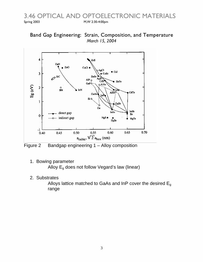
Figure 2 Bandgap engineering 1 – Alloy composition
1. Bowing parameter Alloy Eg does not follow Vegard’s law (linear)
2. Substrates Alloys lattice matched to GaAs and InP cover the desired Eg
range
3

3.46 OPTICAL AND OPTOELECTRONIC MATERIALS Spring 2003 M,W 2:30-4:00pm
Band Gap Engineering: Strain, Composition, and Temperature March 15, 2004
Figure 4 Lattice-matched InGaAsP on InP for 1.55 and 1.31 m laser
diode.
4

3.46 OPTICAL AND OPTOELECTRONIC MATERIALS Spring 2003 M,W 2:30-4:00pm
Band Gap Engineering: Strain, Composition, and Temperature March 15, 2004
Figure 5 Bandgap engineering 2: Quantum Confinement Dimensions < Bohr orbit in dielectric medium Quantum size effect: En=n2h2/8mL2
Bandgap discontinuity : C= e1- e2 (Anderson’s rule) AlGaAs/GaAs C = 0.65 G (0.85 0.57 0.70 0.65)
5

3.46 OPTICAL AND OPTOELECTRONIC MATERIALS Spring 2003 M,W 2:30-4:00pm
Band Gap Engineering: Strain, Composition, and Temperature March 15, 2004
Figure 6 Erbium Doped Fiber Amplifier (EDFA) Pump Light Sources 1. Pump light source at 980nm
Shorter wavelengths: GaAs Longer wavelengths: InP
2. Ternary alloy requires strain tuning of Eg
Strained In0.2GaAs/GaAs
6

3.46 OPTICAL AND OPTOELECTRONIC MATERIALS Spring 2003 M,W 2:30-4:00pm
Band Gap Engineering: Strain, Composition, and Temperature March 15, 2004
Figure 7 Strain and strain relaxation (dislocations) 1. Critical layer thickness
InxGaAs/GaAs 2. Strained layers
GaAs/GaAs MQW LDs on GaAs substrate
7

3.46 OPTICAL AND OPTOELECTRONIC MATERIALS Spring 2003 M,W 2:30-4:00pm
Band Gap Engineering: Strain, Composition, and Temperature March 15, 2004
Figure 8 Biaxial-strained semiconductor bandgap 1. Deformation potentials
Band extrema 2. Quantum confined states
LH (light hole) HH (heavy hole)
8

3.46 OPTICAL AND OPTOELECTRONIC MATERIALS Spring 2003 M,W 2:30-4:00pm
Band Gap Engineering: Strain, Composition, and Temperature March 15, 2004
Figure 9 Absorption coefficient of Ge and Si 1. Choice of detector material
Monolithic integration with receiver electronics
9
3.46 OPTICAL AND OPTOELECTRONIC MATERIALS Spring 2003 M,W 2:30-4:00pm
Band Gap Engineering: Strain, Composition, and Temperature March 15, 2004
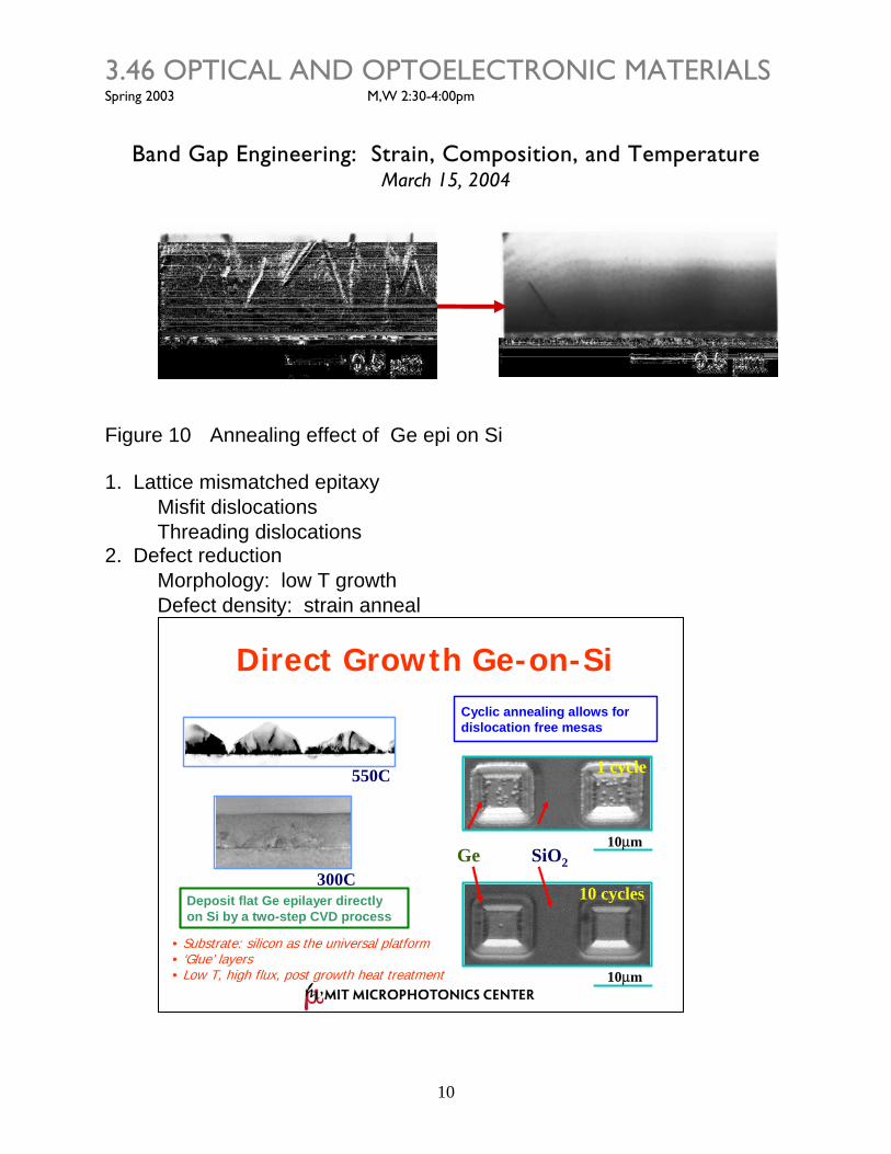
Figure 10 Annealing effect of Ge epi on Si 1. Lattice mismatched epitaxy
Misfit dislocations Threading dislocations
2. Defect reduction Morphology: low T growth Defect density: strain anneal
Direct Growth Ge-on-Si
Deposit flat Ge epilayer directly on Si by a two-step CVD process
550C
300C
10µm
10 cycles
10µmGe SiO2
1 cycle
Cyclic annealing allows for dislocation free mesas
• Substrate: silicon as the universal platform• ‘Glue’ layers• Low T, high flux, post growth heat treatment
10
3.46 OPTICAL AND OPTOELECTRONIC MATERIALS Spring 2003 M,W 2:30-4:00pm
Band Gap Engineering: Strain, Composition, and Temperature March 15, 2004
Silicon Microphotonics, Massachusetts Institute of Technology
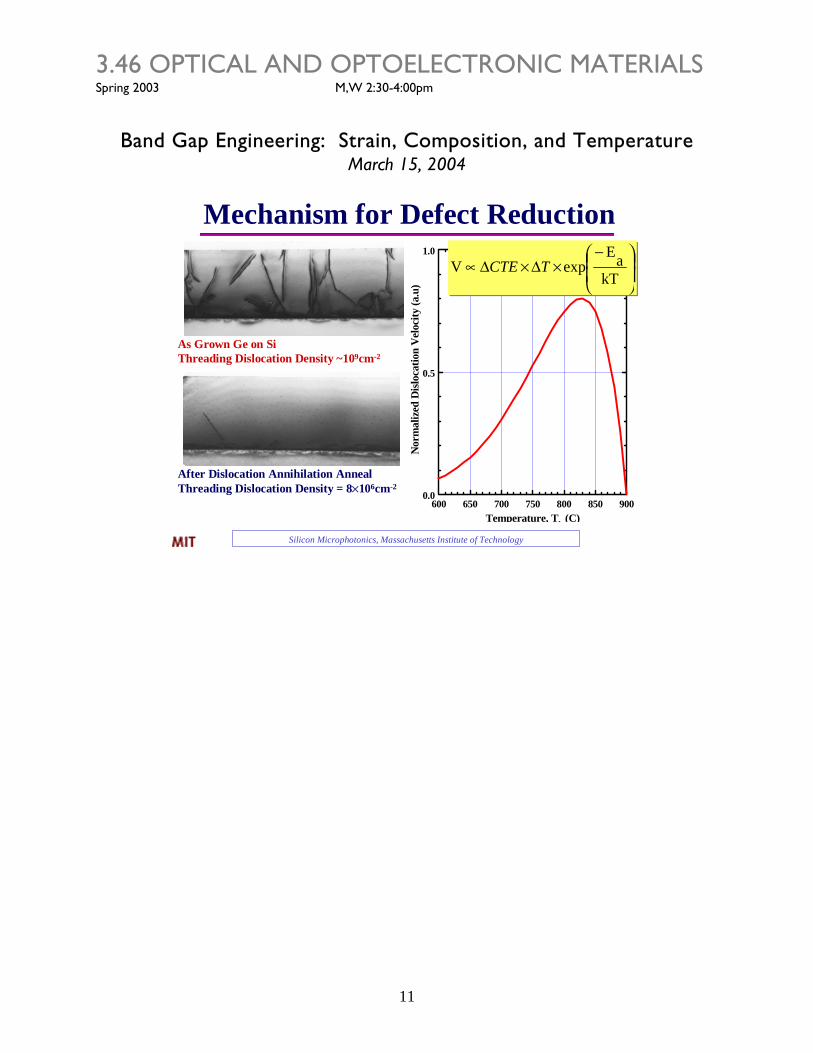
Mechanism for Defect Reduction
After Dislocation Annihilation AnnealThreading Dislocation Density = 8×106cm-2
600 650 700 750 800 850 9000.0
0.5
1.0
Nor
mal
ized
Disl
ocat
ion
Vel
ocity
(a.u
)
Temperature, TL (C)
⎟⎟⎠
⎞⎜⎜⎝
⎛ −×∆×∆∝
kTaE
expV TCTE
As Grown Ge on SiThreading Dislocation Density ~109cm-2
11

3.46 OPTICAL AND OPTOELECTRONIC MATERIALS Spring 2003 M,W 2:30-4:00pm
Band Gap Engineering: Strain, Composition, and Temperature March 15, 2004
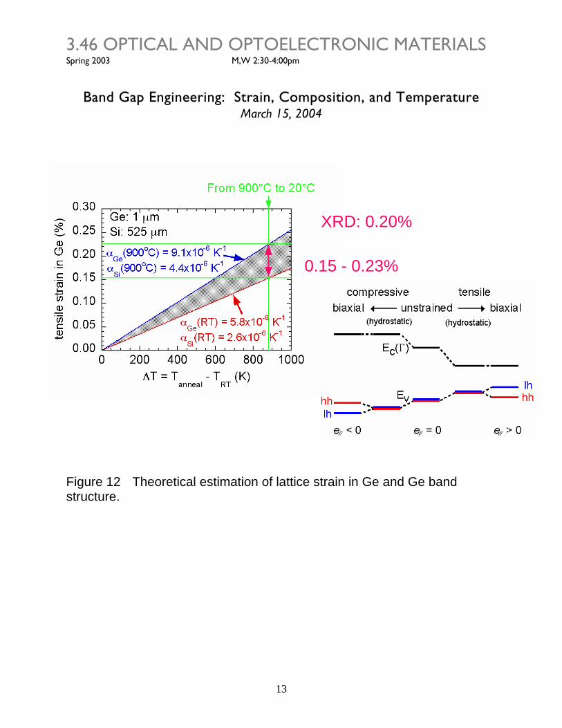
Effect of lattice strain in Ge layer grown on Si Bandgap change absorption property
Possible strain Compressive: lattice mismatch
Lattice constant: Ge 5.66 Å > Si 5.43 Å Tensile: thermal mismatch
Expansion coefficient: Ge 5.9x10⁻⁶ K-1 > Si 2.6x10⁻⁶ K-1
Thermal expansion mismatch - Bi-metal effectRoom temp. Equilibrium at high temp.
Tensile strain in Gei
Thermal expansion coefficient: Ge > S Figure 11 Annealing effect of Ge on Si12
3.46 OPTICAL AND OPTOELECTRONIC MATERIALS Spring 2003 M,W 2:30-4:00pm
Band Gap Engineering: Strain, Composition, and Temperature March 15, 2004
XRD: 0.20%
0.15 - 0.23%
Figure 12 Theoretical estimation of lattice strain in Ge and Ge band structure.
13

3.46 OPTICAL AND OPTOELECTRONIC MATERIALS Spring 2003 M,W 2:30-4:00pm
Band Gap Engineering: Strain, Composition, and Temperature March 15, 2004
14
Figure 13 Deformation potential calculation for enhanced long wavelength absorption coefficient
30 meV bandgap shrinkage and L-band optical wavelength detection
15
Wavelength (nm)
Abs
orpt
ion
Coe
ffici
ent (
cm-1
)
10 2
10 3
10 4
1400 1450 1500 1550 1600 1650
Ge/Si (MIT)
Bulk Ge
C-band L-band
0.0 0.1 0.2 0.30.75
0.76
0.77
0.78
0.79
0.80
1640
1620
1600
1580
1560
Ge/Si/C54-TiSi2 Ge/Si Bulk Ge
EgΓ (lh
) (e
V)
In plane strain (%)
Wavelength(nm
)
Extended Response of Ge-on-Si Strained Epitaxial Layers
Strained Ge layers show absorption spectrum ‘red’ shift of ~30 nm.
Cannon, Jongthammanurak, Liu, MIT
Ge Band Structure
Tensile strain shifts light hole band up in energy with respect to heavy hole band, reducing direct band gap