32-bit microcontrollers v850 pf - usbid · 32-bit microcontrollers v850 ... performance of v850...
TRANSCRIPT

32-bit Microcontrollers
V850
See your creations come to lifethrough the unsurpassedperformance of V850 microcontrollers.
NEC Electronics Corporation1753, Shimonumabe, Nakahara-ku,Kawasaki, Kanagawa 211-8668, JapanTel: 044-435-5111http://www.necel.com/
[America]
NEC Electronics America, Inc.2880 Scott Blvd.Santa Clara, CA 95050-2554, U.S.A.Tel: 408-588-6000 800-366-9782http://www.am.necel.com/
[Asia & Oceania]
NEC Electronics (China) Co., Ltd7th Floor, Quantum Plaza, No. 27 ZhiChunLu HaidianDistrict, Beijing 100083, P.R.ChinaTel: 010-8235-1155http://www.cn.necel.com/
Shanghai BranchRoom 2509-2510, Bank of China Tower,200 Yincheng Road Central,Pudong New Area, Shanghai, P.R.China P.C:200120Tel:021-5888-5400http://www.cn.necel.com/
Shenzhen BranchUnit 01, 39/F, Excellence Times Square Building,No. 4068 Yi Tian Road, Futian District, Shenzhen,P.R.China P.C:518048Tel:0755-8282-9800http://www.cn.necel.com/
NEC Electronics Hong Kong Ltd.Unit 1601-1613, 16/F., Tower 2, Grand Century Place,193 Prince Edward Road West, Mongkok, Kowloon, Hong KongTel: 2886-9318http://www.hk.necel.com/
NEC Electronics Taiwan Ltd.7F, No. 363 Fu Shing North RoadTaipei, Taiwan, R. O. C.Tel: 02-8175-9600http://www.tw.necel.com/
NEC Electronics Singapore Pte. Ltd.238A Thomson Road, #12-08 Novena Square, Singapore 307684Tel: 6253-8311http://www.sg.necel.com/
NEC Electronics Korea Ltd.11F., Samik Laviedʼor Bldg., 720-2,Yeoksam-Dong, Kangnam-Ku,Seoul, 135-080, KoreaTel: 02-558-3737http://www.kr.necel.com/
For further information, please contact:
G0706
[Europe]
NEC Electronics (Europe) GmbHArcadiastrasse 1040472 Düsseldorf, GermanyTel: 0211-65030http://www.eu.necel.com/
Hanover OfficePodbielskistrasse 166 B30177 HannoverTel: 0 511 33 40 2-0Munich OfficeWerner-Eckert-Strasse 981829 MünchenTel: 0 89 92 10 03-0Stuttgart OfficeIndustriestrasse 370565 StuttgartTel: 0 711 99 01 0-0United Kingdom BranchCygnus House, Sunrise ParkwayLinford Wood, Milton KeynesMK14 6NP, U.K.Tel: 01908-691-133Succursale Française9, rue Paul Dautier, B.P. 5278142 Velizy-Villacoublay CédexFranceTel: 01-3067-5800Sucursal en EspañaJuan Esplandiu, 1528007 Madrid, SpainTel: 091-504-2787Tyskland FilialTäby CentrumEntrance S (7th floor)18322 Täby, SwedenTel: 08 638 72 00Filiale ItalianaVia Fabio Filzi, 25/A20124 Milano, ItalyTel: 02-667541Branch The NetherlandsSteijgerweg 65616 HS EindhovenThe NetherlandsTel: 040 265 40 10
Document No. U15412EJ8V0PF00 (8th edition)Date Published January 2009 N © NEC Electronics Corporation 2002, 2004 January 2009

� Pamphlet U15412EJ8V0PF
V850 Product Roadmap • • • • • •
NEC Electronics Microcontroller Deployment •
Application Examples • • • • • • •
5 Keys of V850 • • • • • • • • • • • • •
Low-End Lineup (5 V Operation) •
Low-End Lineup (3 V Operation) • High-End Lineup • • • • • • • • • • • • ASSP Lineup (Inverter Control, etc.) • • •
ASSP Lineup (CAN) • • • • • • • • • • •
ASSP Lineup (IEBusTM) • • • • • • • • •
Memory Lineup • • • • • • • • • • • • • Package Lineup • • • • • • • • • • • • •
CPU Roadmap • • • • • • • • • • • • • •
CPU Function Comparison • • • •
System LSI Support • • • • • • • • •
V850 Common Architecture • • •
V850E1, V850ES Architecture • • •
V850E2 Architecture • • • • • • • • •
Memory Access Functions • • • •
Analog Circuits • • • • • • • • • • • • •
Timer/Counter • • • • • • • • • • • • •
Serial Interface • • • • • • • • • • • • • • Other • • • • • • • • • • • • • • • • • • • • • •
All Flash 32-bit USB MCU(V850ES/Jx3-H, V850ES/Jx3-U) • • • • •
V850 Benchmark • • • • • • • • • • • Low Power Consumption • • • •
Noise Countermeasures • • • • • •
Solutions for V850 • • • • • • • • •
Rotating • • • • • • • • • • • • • • • • • •
Speaking • • • • • • • • • • • • • • • • • •
Showing • • • • • • • • • • • • • • • • • • •
Connecting • • • • • • • • • • • • • • •
Features • • • • • • • • • • • • • • • • • • • •
Rewrite Modes • • • • • • • • • • • • •
Flash Specification List • • • • • • •
Flash Memory Programmers • •
Low-End Lineup (5 V Operation) •
Low-End Lineup (3 V Operation) • High-End Lineup • • • • • • • • • • • •
ASSP Lineup (Inverter Control, etc.) • •
ASSP Lineup (CAN) • • • • • • • • •
ASSP Lineup (IEBus) • • • • • • • • •
Low-Priced Development Environment Lineup(All Flash Microcontrollers) • • • • • • • • • • •
Development Flow • • • • • • • • • •
Development Tools • • • • • • • • • •
V850 Development Environment • • • Software Products • • • • • • • • • • •
Hardware Products • • • • • • • • • •
The V850 high-performance microcontrollers answer many different application system needs. They realize extremely low power consumption and low noise while offering high performance and a wide array of functions. The broad V850 product lineup provides optimum solutions for the next-generation systems of our customers.
04
08
24
32
40
42
44
48
84
V850 Website • • • • • • • • • • • • • • •95
INDEX
455
6
8101214
16182022
242425
263031
323234
404041
3536
38
42424243
43
444445
46
485464
667079
858686
95
889093
High performance
Performance range from20 to over 400 MIPS with a
single instruction set
Product deployment
Low-end/high-end/ASSP deployment
Additional functions
Rich solutionlineup
System LSIs
Smooth transition tosystem LSIs
Development environment
Rich developmentenvironment lineup
Roadmap/Features
Product Lineup
CPU
Variety of Peripheral Functions
Performance
Solution
Flash
Product Specification List
Development Environment
Information Dissemination
Pamphlet U15412EJ8V0PF�

Pamphlet U15412EJ8V0PF �
V850 Product Roadmap • • • • • •
NEC Electronics Microcontroller Deployment •
Application Examples • • • • • • •
5 Keys of V850 • • • • • • • • • • • • •
Low-End Lineup (5 V Operation) •
Low-End Lineup (3 V Operation) • High-End Lineup • • • • • • • • • • • • ASSP Lineup (Inverter Control, etc.) • • •
ASSP Lineup (CAN) • • • • • • • • • • •
ASSP Lineup (IEBusTM) • • • • • • • • •
Memory Lineup • • • • • • • • • • • • • Package Lineup • • • • • • • • • • • • •
CPU Roadmap • • • • • • • • • • • • • •
CPU Function Comparison • • • •
System LSI Support • • • • • • • • •
V850 Common Architecture • • •
V850E1, V850ES Architecture • • •
V850E2 Architecture • • • • • • • • •
Memory Access Functions • • • •
Analog Circuits • • • • • • • • • • • • •
Timer/Counter • • • • • • • • • • • • •
Serial Interface • • • • • • • • • • • • • • Other • • • • • • • • • • • • • • • • • • • • • •
All Flash 32-bit USB MCU(V850ES/Jx3-H, V850ES/Jx3-U) • • • • •
V850 Benchmark • • • • • • • • • • • Low Power Consumption • • • •
Noise Countermeasures • • • • • •
Solutions for V850 • • • • • • • • •
Rotating • • • • • • • • • • • • • • • • • •
Speaking • • • • • • • • • • • • • • • • • •
Showing • • • • • • • • • • • • • • • • • • •
Connecting • • • • • • • • • • • • • • •
Features • • • • • • • • • • • • • • • • • • • •
Rewrite Modes • • • • • • • • • • • • •
Flash Specification List • • • • • • •
Flash Memory Programmers • •
Low-End Lineup (5 V Operation) •
Low-End Lineup (3 V Operation) • High-End Lineup • • • • • • • • • • • •
ASSP Lineup (Inverter Control, etc.) • •
ASSP Lineup (CAN) • • • • • • • • •
ASSP Lineup (IEBus) • • • • • • • • •
Low-Priced Development Environment Lineup(All Flash Microcontrollers) • • • • • • • • • • •
Development Flow • • • • • • • • • •
Development Tools • • • • • • • • • •
V850 Development Environment • • • Software Products • • • • • • • • • • •
Hardware Products • • • • • • • • • •
The V850 high-performance microcontrollers answer many different application system needs. They realize extremely low power consumption and low noise while offering high performance and a wide array of functions. The broad V850 product lineup provides optimum solutions for the next-generation systems of our customers.
04
08
24
32
40
42
44
48
84
V850 Website • • • • • • • • • • • • • • •95
INDEX
455
6
8101214
16182022
242425
263031
323234
404041
3536
38
42424243
43
444445
46
485464
667079
858686
95
889093
High performance
Performance range from20 to over 400 MIPS with a
single instruction set
Product deployment
Low-end/high-end/ASSP deployment
Additional functions
Rich solutionlineup
System LSIs
Smooth transition tosystem LSIs
Development environment
Rich developmentenvironment lineup
Roadmap/Features
Product Lineup
CPU
Variety of Peripheral Functions
Performance
Solution
Flash
Product Specification List
Development Environment
Information Dissemination

� Pamphlet U15412EJ8V0PF
Automotive
Audio
Portable devices
Cameras
Computer peripherals
Home appliances
Industrial equipment
Video andrecording equipment
Other
The V850 microcontrollers are suitable for various applicationfields and raise the commercial value of customer systems.
Engines, car infotainment, dashboards,power steering, ABS
Portable audio, component stereo systems, home theater
PDAs, IC recorders
DVC, DSC, SLR cameras
LBP, PPC, MFP, inkjet printers, scanners,fax machines
Air conditioners, refrigerators, washing machines,microwave ovens
Industrial motors, control equipment,vending machines, power meters
DVD players, DVD recorders,industrial cameras
Electronic instruments, electric bidets, toys,learning devices, remote controllers, etc.
V850E2 CPU
V850E1 CPU
V850 CPU
V850ES CPU
High-end lineup
Low-end lineup
ASSP lineupHigh-end lineup
Low-end lineup
ASSP lineup
• Frequency: 33 to 200 MHz • Memory size: ROM: ROMless to 512 KB
RAM: 4 to 200 KB • Package: 100 to 176 pins (QFP & FBGA)
Inverter control
DVC control
Car infotainment control
Power meter control
Dashboard control
• Frequency: 13 to 80 MHz• Memory size: ROM: ROMless to
2048 KBRAM: 4 to 92 KB
• Package: 64 to 257 pins(QFP & FBGA)
• Frequency: 16 to 48 MHz • Memory size: ROM: ROMless to 1024 KB
RAM: 4 to 60 KB • Package: 64 to 144 pins (QFP & FBGA)
High cost-performance
High performance: On-chip MEMC/DMA
V850E2 CPU
200 MHz @ 432 MIPS
V850E1 CPU
V850 CPU
V850ES CPU
150 MHz @ 323 MIPS
48 MHz @ 98 MIPS
33 MHz @ 38 MIPS
Field-specific lineupsStandard lineups
Roadmap/Features
V850 Product Roadmap NEC Electronics Microcontroller Deployment
Application Examples
Up
war
d c
om
pat
ible
inst
ruct
ion
set
s
An expanding product lineup of continuously evolving V850 microcontrollers
Hig
h pe
rform
ance
Price
78K078K4
32-bit RISC
8/16-bit CISC
4 to 16-bit applications17K
75X/XL
Low-end lineup
ASSP lineup
High-end lineup
78K0SSystem control
Data processing
D6X
78K0R
32-bit applications

Pamphlet U15412EJ8V0PF �
Automotive
Audio
Portable devices
Cameras
Computer peripherals
Home appliances
Industrial equipment
Video andrecording equipment
Other
The V850 microcontrollers are suitable for various applicationfields and raise the commercial value of customer systems.
Engines, car infotainment, dashboards,power steering, ABS
Portable audio, component stereo systems, home theater
PDAs, IC recorders
DVC, DSC, SLR cameras
LBP, PPC, MFP, inkjet printers, scanners,fax machines
Air conditioners, refrigerators, washing machines,microwave ovens
Industrial motors, control equipment,vending machines, power meters
DVD players, DVD recorders,industrial cameras
Electronic instruments, electric bidets, toys,learning devices, remote controllers, etc.
V850E2 CPU
V850E1 CPU
V850 CPU
V850ES CPU
High-end lineup
Low-end lineup
ASSP lineupHigh-end lineup
Low-end lineup
ASSP lineup
• Frequency: 33 to 200 MHz • Memory size: ROM: ROMless to 512 KB
RAM: 4 to 200 KB • Package: 100 to 176 pins (QFP & FBGA)
Inverter control
DVC control
Car infotainment control
Power meter control
Dashboard control
• Frequency: 13 to 80 MHz• Memory size: ROM: ROMless to
2048 KBRAM: 4 to 92 KB
• Package: 64 to 257 pins(QFP & FBGA)
• Frequency: 16 to 48 MHz • Memory size: ROM: ROMless to 1024 KB
RAM: 4 to 60 KB • Package: 64 to 144 pins (QFP & FBGA)
High cost-performance
High performance: On-chip MEMC/DMA
V850E2 CPU
200 MHz @ 432 MIPS
V850E1 CPU
V850 CPU
V850ES CPU
150 MHz @ 323 MIPS
48 MHz @ 98 MIPS
33 MHz @ 38 MIPS
Field-specific lineupsStandard lineups
Roadmap/Features
V850 Product Roadmap NEC Electronics Microcontroller Deployment
Application Examples
Up
war
d c
om
pat
ible
inst
ruct
ion
set
sAn expanding product lineup of continuously evolving V850 microcontrollers
Hig
h pe
rform
ance
Price
78K078K4
32-bit RISC
8/16-bit CISC
4 to 16-bit applications17K
75X/XL
Low-end lineup
ASSP lineup
High-end lineup
78K0SSystem control
Data processing
D6X
78K0R
32-bit applications

� Pamphlet U15412EJ8V0PF
PFESiP® EP-1Note
Note PFESiP EP-1 and PFESiP EP-3 are custom microcontrollers that integrate a V850 microcontroller and logic LSI.
Processes
System
IP cores
Design environment
Micro-fabrication technologyMulti-layer wiring technologyMixed-process technologyHigh-pin-count packages
MPU, DSP, DRAM,SRAM, AV, communication,BUS, high-speed I/O
Chip design environmentSynthesis/verificationSoftware development environmentHardware/software coordinated design
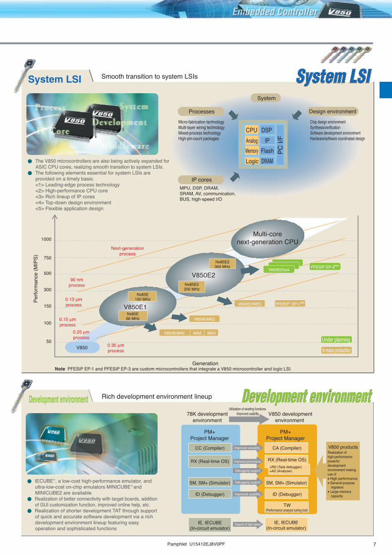
System LSI Smooth transition to system LSIs
• The V850 microcontrollers are also being actively expanded for ASIC CPU cores, realizing smooth transition to system LSIs.
• The following elements essential for system LSIs are provided on a timely basis: <1> Leading-edge process technology <2> High-performance CPU core <3> Rich lineup of IP cores <4> Top-down design environment <5> Flexible application design
CPUAnalog
LogicMemory Flash
DSP
DRAM
IP
System LSI
Development environment Rich development environment lineup
• IECUBE, a low-cost high-performance emulator, and ultra-low-cost on-chip emulators MINICUBE and MINICUBE2 are available.
• Realization of better connectivity with target boards, addition of GUI customization function, improved online help, etc.
• Realization of shorter development TAT through support of quick and accurate software development via a rich development environment lineup featuring easy operation and sophisticated functions
PM+Project Manager
+RD (Task debugger) +AZ (Analyzer)
PM+Project Manager
Improved versatility
Improved performance
Improved usability
Debugging support
Support of high speed
V850 developmentenvironment
78K developmentenvironment
V850 productsCC (Compiler) CA (Compiler)
RX (Real-time OS) RX (Real-time OS)
SM, SM+ (Simulator)
ID (Debugger)
SM, SM+ (Simulator)
ID (Debugger)
TW(Performance analysis tuning tool)
IE, IECUBE(In-circuit emulator)
IE, IECUBE(In-circuit emulator)
Utilization of existing functions Improved usability
Debugging support
Development environment
Product lineup Low-end/High-end/ASSP deployment
• Low-end lineup: General-purpose microcontrollers for the 16- to 32-bit market designed for high cost-performance
• High-end lineup: Designed for high performance, on-chip memory controller and DMA
• ASSP lineup: Field-specific product lineup, on-chip dedicated hardware
Communication
High performance
On-chip dedicatedhardware
Low noise,low power consumption
High cost-performance
Industrial
Homeappliances
Consumerelectronics
Officeequipment
Automotive
Additional functions Rich solution lineup
• Realization of systems with high added value through the addition of supplementary functions to existing systems via middleware
• Realization of functions heretofore realized with peripheral ICs using V850 and middleware, reducing development time and reducing system costs
Portable devices
Electronicdictionaries
Telephones
Homeappliances
Carinfotainment
JavaTMNote
H.264
BrowsersNote
SpeechrecognitionNote
SpeechsynthesisNote
ADPCM
Additional functions
Product lineup
V850E1 CPU
V850E2 CPU
V850ES CPU
V850 CPU
V850E/MxxV850E2/Mxx
High-end lineup
V850E/xxxV850ES/xxxV850/xxx
ASSP lineup
V850ES/JxxV850ES/KxxV850ES/SxxV850/Sxx
Low-end lineup (3 V)
V850ES/HxxV850ES/KxxV850/Sxx
Low-end lineup (5 V)
Next-generationprocess
0.15 mmprocess
0.13 mmprocess
90 nmprocess
0.35 mmprocess
Perfo
rman
ce (M
IPS)
Generation
100
300
500
1000
50
150
750
MA3
V850E/ME2
MA2V850E/MA1
V850
V850E2/ME3
Multi-corenext-generation CPU
V850E2/xxx
Nx85E2300 MHz
Nx85E2200 MHz
V850E2
Nx85E150 MHz
Nx85E66 MHz
V850E1
PC I/
F
Realization of high-performance powerful development environment making use of • High performance • General-purpose
registers • Large memory
capacityTCP/IP
File systems IrDANote
Image processing
Networks
Amusement machines
ToysHuman interfaces
AV equipment
JPEG
DSC
Middleware
Note Middleware from partner company is used.
0.25 mmprocess
PFESiP EP-3Note
Under planningIn mass production
High performance Performance ranging from 20 to over 400 MIPS with a single instruction set
• Compared to 8-/16-bit microcontrollers, offers MIPS performance that is at least 10 times higher for the same frequency, and 2 to 3 times higher at the actual application level (based on NEC Electronics evaluation).
• System operation at frequencies 1/2 to 1/3 those of 8-/16-bit microcontrollers is enabled, contributing to lowering system power consumption.
• The V850 CPU, V850ES CPU, V850E1 CPU, and V850E2 CPU are upward compatible at the object level.
Processor products
Not compatible
Compatible atobject level!
Not compatible
Data processing
System control
Compatible with up tomiddle-range class
Compatible with up to high-end classmodels with MIPS performance of10 times higher
V850ESV850
V850E1
V850ESV850
V850E2
Othermanufacturers' 16-bit
microcontrollers
Othermanufacturers' 32-bit
microcontrollers
33 MHz
20 MHz
150 MHz
≥ 200 MHz
High performance
5 Keys of V850 5 points supporting the high performance of the V850 microcontrollers
Roadmap/Features
Pamphlet U15412EJ8V0PF �
PFESiP® EP-1Note
Note PFESiP EP-1 and PFESiP EP-3 are custom microcontrollers that integrate a V850 microcontroller and logic LSI.
Processes
System
IP cores
Design environment
Micro-fabrication technologyMulti-layer wiring technologyMixed-process technologyHigh-pin-count packages
MPU, DSP, DRAM,SRAM, AV, communication,BUS, high-speed I/O
Chip design environmentSynthesis/verificationSoftware development environmentHardware/software coordinated design
System LSI Smooth transition to system LSIs
• The V850 microcontrollers are also being actively expanded for ASIC CPU cores, realizing smooth transition to system LSIs.
• The following elements essential for system LSIs are provided on a timely basis: <1> Leading-edge process technology <2> High-performance CPU core <3> Rich lineup of IP cores <4> Top-down design environment <5> Flexible application design
CPUAnalog
LogicMemory Flash
DSP
DRAM
IP
System LSI
Development environment Rich development environment lineup
• IECUBE, a low-cost high-performance emulator, and ultra-low-cost on-chip emulators MINICUBE and MINICUBE2 are available.
• Realization of better connectivity with target boards, addition of GUI customization function, improved online help, etc.
• Realization of shorter development TAT through support of quick and accurate software development via a rich development environment lineup featuring easy operation and sophisticated functions
PM+Project Manager
+RD (Task debugger) +AZ (Analyzer)
PM+Project Manager
Improved versatility
Improved performance
Improved usability
Debugging support
Support of high speed
V850 developmentenvironment
78K developmentenvironment
V850 productsCC (Compiler) CA (Compiler)
RX (Real-time OS) RX (Real-time OS)
SM, SM+ (Simulator)
ID (Debugger)
SM, SM+ (Simulator)
ID (Debugger)
TW(Performance analysis tuning tool)
IE, IECUBE(In-circuit emulator)
IE, IECUBE(In-circuit emulator)
Utilization of existing functions Improved usability
Debugging support
Development environment
Product lineup Low-end/High-end/ASSP deployment
• Low-end lineup: General-purpose microcontrollers for the 16- to 32-bit market designed for high cost-performance
• High-end lineup: Designed for high performance, on-chip memory controller and DMA
• ASSP lineup: Field-specific product lineup, on-chip dedicated hardware
Communication
High performance
On-chip dedicatedhardware
Low noise,low power consumption
High cost-performance
Industrial
Homeappliances
Consumerelectronics
Officeequipment
Automotive
Additional functions Rich solution lineup
• Realization of systems with high added value through the addition of supplementary functions to existing systems via middleware
• Realization of functions heretofore realized with peripheral ICs using V850 and middleware, reducing development time and reducing system costs
Portable devices
Electronicdictionaries
Telephones
Homeappliances
Carinfotainment
JavaTMNote
H.264
BrowsersNote
SpeechrecognitionNote
SpeechsynthesisNote
ADPCM
Additional functions
Product lineup
V850E1 CPU
V850E2 CPU
V850ES CPU
V850 CPU
V850E/MxxV850E2/Mxx
High-end lineup
V850E/xxxV850ES/xxxV850/xxx
ASSP lineup
V850ES/JxxV850ES/KxxV850ES/SxxV850/Sxx
Low-end lineup (3 V)
V850ES/HxxV850ES/KxxV850/Sxx
Low-end lineup (5 V)
Next-generationprocess
0.15 mmprocess
0.13 mmprocess
90 nmprocess
0.35 mmprocess
Perfo
rman
ce (M
IPS)
Generation
100
300
500
1000
50
150
750
MA3
V850E/ME2
MA2V850E/MA1
V850
V850E2/ME3
Multi-corenext-generation CPU
V850E2/xxx
Nx85E2300 MHz
Nx85E2200 MHz
V850E2
Nx85E150 MHz
Nx85E66 MHz
V850E1
PC I/
F
Realization of high-performance powerful development environment making use of • High performance • General-purpose
registers • Large memory
capacityTCP/IP
File systems IrDANote
Image processing
Networks
Amusement machines
ToysHuman interfaces
AV equipment
JPEG
DSC
Middleware
Note Middleware from partner company is used.
0.25 mmprocess
PFESiP EP-3Note
Under planningIn mass production
High performance Performance ranging from 20 to over 400 MIPS with a single instruction set
• Compared to 8-/16-bit microcontrollers, offers MIPS performance that is at least 10 times higher for the same frequency, and 2 to 3 times higher at the actual application level (based on NEC Electronics evaluation).
• System operation at frequencies 1/2 to 1/3 those of 8-/16-bit microcontrollers is enabled, contributing to lowering system power consumption.
• The V850 CPU, V850ES CPU, V850E1 CPU, and V850E2 CPU are upward compatible at the object level.
Processor products
Not compatible
Compatible atobject level!
Not compatible
Data processing
System control
Compatible with up tomiddle-range class
Compatible with up to high-end classmodels with MIPS performance of10 times higher
V850ESV850
V850E1
V850ESV850
V850E2
Othermanufacturers' 16-bit
microcontrollers
Othermanufacturers' 32-bit
microcontrollers
33 MHz
20 MHz
150 MHz
≥ 200 MHz
High performance
5 Keys of V850 5 points supporting the high performance of the V850 microcontrollers
Roadmap/Features

� Pamphlet U15412EJ8V0PF
Product Lineup
Low-End Lineup (5 V Operation)
V853
38 MIPS @ 33 MHz, 4.5 to 5.5 V operation
ROM/RAM: 96 KB/4 KB, 128 KB/4 KB, 256 KB/8 KB
100-pin LQFP
Features
V850ES/HE3, HF3, HG3, HJ3
All Flash products
69 MIPS @ 32 MHz, 66 MIPS @ 32 MHz (µPD70F3757 only),3.7 to 5.5 V operation (A/D converter: 4.0 to 5.5 V)
ROM/RAM: 128 KB/8 KB to 512 KB/32 KB
On-chip multi-channel A/D converter, POC, LVI, DMA,on-chip debug function, motor control function, and SSCG*
64-pin LQFP (HE3), 80-pin LQFP (HF3), 100-pin LQFP (HG3),144-pin LQFP (HJ3)*Spread Spectrum Frequency Synthesizer Clock Generator
V850ES/HE2, HF2, HG2, HJ2
All Flash products43 MIPS @ 20 MHz, 3.5 to 5.5 V operation (A/D converter: 4.0 to 5.5 V)
ROM/RAM: 64 KB/6 KB to 512 KB/20 KB
On-chip multi-channel A/D converter, POC, LVI, DMA, and on-chip debug function
64-pin LQFP (HE2), 80-pin TQFP (HF2), 100-pin LQFP (HG2),144-pin LQFP (HJ2)
V850/SB1
23 MIPS @ 20 MHz, 4.0 to 5.5 V operation
ROM/RAM: 128 KB/8 KB, 256 KB/16 KB, 384 KB/24 KB, 512 KB/24 KB
On-chip DMA (for internal units)
100-pin LQFP/100-pin QFP
V850/SC1
Function-enhanced version of the V850/SB1
23 MIPS @ 20 MHz, 4.0 to 5.5 V operation (flash memory version), 3.5 to 5.5 V operation (mask ROM version)
ROM/RAM: 512 KB/24 KB
On-chip DMA (for internal units)
144-pin LQFP
V850ES/KE1+, KF1+, KG1+, KJ1+
Simple platform development with 8-bit microcontroller 78K0
43 MIPS @ 20 MHz, 2.7 to 5.5 V operation
ROM/RAM: 128 KB/4 KB to 256 KB/16 KB
A wealth of peripheral functions common to 8-bit microcontroller 78K0, on-chip POC, LVI, DMA, and on-chip debug function
64-pin TQFP/64-pin LQFP (KE1+), 80-pin TQFP/80-pin QFP (KF1+),100-pin LQFP/100-pin QFP (KG1+), 144-pin LQFP (KJ1+)
V850ES/KE2, KF2, KG2, KJ2
All Flash products
43 MIPS @ 20 MHz, 2.7 to 5.5 V operation
ROM/RAM: 128 KB/4 KB to 256 KB/16 KB
A wealth of peripheral functions common to 8-bit microcontroller 78K0, on-chip DMA, and on-chip debug function
64-pin LQFP (KE2), 80-pin QFP (KF2),100-pin LQFP/100-pin QFP (KG2), 144-pin LQFP (KJ2)
All Flash lineup
V85033 MHz operation
Kx1+ lineup
V850 lineup
Remark See Product Specification List (pp. 48 to 53) for details on the product specifications.
In massproduction
64-pin 80-pin 100-pin 144-pin 176-pin and higher
V850ES/HE220 MHz, 64-pin
V850ES/HF220 MHz, 80-pin
V850ES/HG220 MHz, 100-pin
V850ES/HJ220 MHz, 144-pin
V850ES/HE332 MHz, 64-pin
V850ES/HF332 MHz, 80-pin
V850ES/HG332 MHz, 100-pin
V850ES/HJ332 MHz, 144-pin
V850ES/KE220 MHz, 64-pin
V850ES/KF220 MHz, 80-pin
V850ES/KG220 MHz, 100-pin
V850ES/KJ220 MHz, 144-pin
V85333 MHz, 100-pin
V850ES/KE1+20 MHz, 64-pin
V850ES/KF1+20 MHz, 80-pin
V850ES/KG1+20 MHz, 100-pin
V850ES/KJ1+20 MHz, 144-pin
V850/SB120 MHz, 100-pin
V850/SC120 MHz, 144-pin

Pamphlet U15412EJ8V0PF �
Product Lineup
Low-End Lineup (5 V Operation)
V853
38 MIPS @ 33 MHz, 4.5 to 5.5 V operation
ROM/RAM: 96 KB/4 KB, 128 KB/4 KB, 256 KB/8 KB
100-pin LQFP
Features
V850ES/HE3, HF3, HG3, HJ3
All Flash products
69 MIPS @ 32 MHz, 66 MIPS @ 32 MHz (µPD70F3757 only),3.7 to 5.5 V operation (A/D converter: 4.0 to 5.5 V)
ROM/RAM: 128 KB/8 KB to 512 KB/32 KB
On-chip multi-channel A/D converter, POC, LVI, DMA,on-chip debug function, motor control function, and SSCG*
64-pin LQFP (HE3), 80-pin LQFP (HF3), 100-pin LQFP (HG3),144-pin LQFP (HJ3)*Spread Spectrum Frequency Synthesizer Clock Generator
V850ES/HE2, HF2, HG2, HJ2
All Flash products43 MIPS @ 20 MHz, 3.5 to 5.5 V operation (A/D converter: 4.0 to 5.5 V)
ROM/RAM: 64 KB/6 KB to 512 KB/20 KB
On-chip multi-channel A/D converter, POC, LVI, DMA, and on-chip debug function
64-pin LQFP (HE2), 80-pin TQFP (HF2), 100-pin LQFP (HG2),144-pin LQFP (HJ2)
V850/SB1
23 MIPS @ 20 MHz, 4.0 to 5.5 V operation
ROM/RAM: 128 KB/8 KB, 256 KB/16 KB, 384 KB/24 KB, 512 KB/24 KB
On-chip DMA (for internal units)
100-pin LQFP/100-pin QFP
V850/SC1
Function-enhanced version of the V850/SB1
23 MIPS @ 20 MHz, 4.0 to 5.5 V operation (flash memory version), 3.5 to 5.5 V operation (mask ROM version)
ROM/RAM: 512 KB/24 KB
On-chip DMA (for internal units)
144-pin LQFP
V850ES/KE1+, KF1+, KG1+, KJ1+
Simple platform development with 8-bit microcontroller 78K0
43 MIPS @ 20 MHz, 2.7 to 5.5 V operation
ROM/RAM: 128 KB/4 KB to 256 KB/16 KB
A wealth of peripheral functions common to 8-bit microcontroller 78K0, on-chip POC, LVI, DMA, and on-chip debug function
64-pin TQFP/64-pin LQFP (KE1+), 80-pin TQFP/80-pin QFP (KF1+),100-pin LQFP/100-pin QFP (KG1+), 144-pin LQFP (KJ1+)
V850ES/KE2, KF2, KG2, KJ2
All Flash products
43 MIPS @ 20 MHz, 2.7 to 5.5 V operation
ROM/RAM: 128 KB/4 KB to 256 KB/16 KB
A wealth of peripheral functions common to 8-bit microcontroller 78K0, on-chip DMA, and on-chip debug function
64-pin LQFP (KE2), 80-pin QFP (KF2),100-pin LQFP/100-pin QFP (KG2), 144-pin LQFP (KJ2)
All Flash lineup
V85033 MHz operation
Kx1+ lineup
V850 lineup
Remark See Product Specification List (pp. 48 to 53) for details on the product specifications.
In massproduction
64-pin 80-pin 100-pin 144-pin 176-pin and higher
V850ES/HE220 MHz, 64-pin
V850ES/HF220 MHz, 80-pin
V850ES/HG220 MHz, 100-pin
V850ES/HJ220 MHz, 144-pin
V850ES/HE332 MHz, 64-pin
V850ES/HF332 MHz, 80-pin
V850ES/HG332 MHz, 100-pin
V850ES/HJ332 MHz, 144-pin
V850ES/KE220 MHz, 64-pin
V850ES/KF220 MHz, 80-pin
V850ES/KG220 MHz, 100-pin
V850ES/KJ220 MHz, 144-pin
V85333 MHz, 100-pin
V850ES/KE1+20 MHz, 64-pin
V850ES/KF1+20 MHz, 80-pin
V850ES/KG1+20 MHz, 100-pin
V850ES/KJ1+20 MHz, 144-pin
V850/SB120 MHz, 100-pin
V850/SC120 MHz, 144-pin

10 Pamphlet U15412EJ8V0PF
Product Lineup
Low-End Lineup (3 V Operation)
Features
All Flash lineup
V850 super low-end
Kx1+ lineup
Note 2.5 V operationRemark See Product Specification List (pp. 54 to 63) for details on the product specifications.
SAx lineup
Sxx lineup
ROMlessInternal RAM: 48 KB
V850ES/JG3-H, JH3-H, JG3-U, JH3-U
All Flash products
98 MIPS @ 48 MHz, 2.85 to 3.6 V operation (A/D converter, USB controller: 3.0 to 3.6 V)
ROM/RAM: 256 KB/40 KB* to 512 KB/56 KB*
USB controller: USB 2.0 function (full-speed) × 1 ch,USB 2.0 host (full-speed) × 1 ch (JG3-U, JH3-U only)
100-pin LQFP (JG3-H, JG3-U), 128-pin LQFP (JH3-H, JH3-U)* 8 KB of data-only RAM included.
V850ES/JG3, JJ3
All Flash products
69 MIPS @ 32 MHz, 2.85 to 3.6 V operation (A/D converter: 3.0 to 3.6 V)
ROM/RAM: 384 KB/32 KB, 512 KB/40 KB, 768 KB/60 KB, 1024 KB/60 KB
Function and pin compatibility with V850ES/Jx2, and permits appropriation of Jx2 development environment
On-chip multi-channel serial interface, LVI, clock monitor, DMA, and on-chip debug function
5 V withstand voltage ports incorporated, and 5 V output is possible by setting N-ch open-drain output
100-pin LQFP (JG3), 144-pin LQFP (JJ3)
V850ES/JG2, JJ2
All Flash products
43 MIPS @ 20 MHz, 2.85 to 3.6 V operation (A/D converter: 3.0 to 3.6 V)
ROM/RAM: 128 KB/12 KB, 256 KB/24 KB, 384 KB/32 KB,512 KB/40 KB, 640 KB/48 KB
On-chip multi-channel serial interface, LVI, clock monitor, DMA, and on-chip debug function
5 V withstand voltage ports incorporated, and 5 V output is possible by setting N-ch open-drain output
100-pin LQFP (JG2), 100-pin QFP (JG2 (ROM: 128 KB/256 KB/384 KB versions only)), 144-pin LQFP (JJ2)
V850ES/KE2, KF2, KG2, KJ2
All Flash products
22 MIPS @ 10 MHz, 2.7 to 5.5 V operation
ROM/RAM: 128 KB/4 KB to 256 KB/16 KB
A wealth of peripheral functions common to 8-bit microcontroller 78K0, on-chip DMA, and on-chip debug function
64-pin LQFP (KE2), 80-pin QFP (KF2),100-pin LQFP/100-pin QFP (KG2), 144-pin LQFP (KJ2)
V850ES/SG2-H, SJ2-H
66 MIPS @ 32 MHz, 3.0 to 3.6 V operation
ROM/RAM: 512 KB/40 KB, 640 KB/48 KB
On-chip multi-channel serial interface, clock monitor, CRC, DMA, andon-chip debug function
5 V withstand voltage ports incorporated, and 5 V output is possible bysetting N-ch open-drain output
100-pin LQFP (SG2-H), 144-pin LQFP (SJ2-H)
V850ES/ST2
ROMless product with large-capacity RAM
34 MHz, 3.0 to 3.6 V operation
ROM/RAM: ROMless/48 KB
120-pin TQFP/144-pin LQFP
V850/SA1
23 MIPS @ 20 MHz, 2.7 to 3.6 V operation
ROM/RAM: 64 KB/4 KB, 128 KB/4 KB, 256 KB/8 KB
Low power operation 66 mW (3.3 V, 20 MHz), on-chip DMA (for internal units)
100-pin LQFP/121-pin FBGA
V850ES/SG2, SJ2
43 MIPS @ 20 MHz, 2.85 to 3.6 V operation (A/D converter: 3.0 to 3.6 V)
ROM/RAM: 256 KB/24 KB, 384 KB/32 KB, 512 KB/40 KB, 640 KB/48 KB
On-chip multi-channel serial interface, LVI, clock monitor, CRC, DMA, and on-chip debug function
5 V withstand voltage ports incorporated, and 5 V output is possible by setting N-ch open-drain output
100-pin LQFP (SG2), 100-pin QFP (SG2 (ROM: 256 KB/384 KBversions only)), 144-pin LQFP (SJ2)
V850ES/KE1+, KF1+, KG1+, KJ1+
Simple platform development with 8-bit microcontroller 78K0
22 MIPS @ 10 MHz, 2.7 to 5.5 V operation
ROM/RAM: 128 KB/4 KB to 256 KB/16 KB
A wealth of peripheral functions common to 8-bit microcontroller 78K0, on-chip POC, LVI, DMA, and on-chip debug function
64-pin TQFP/64-pin LQFP (KE1+), 80-pin TQFP/80-pin QFP (KF1+), 100-pin LQFP/100-pin QFP (KG1+), 144-pin LQFP (KJ1+)
V850ES/SG1
Part of V850ES/SG2 lineup
43 MIPS @ 20 MHz, 2.85 to 3.6 V operation (A/D converter: 3.0 to 3.6 V)
ROM/RAM: 256 KB/12 KB
On-chip clock monitor
5 V withstand voltage ports incorporated, and 5 V output is possible by setting N-ch open-drain output
100-pin LQFP/100-pin QFP
V850ES/SA2, SA3
Low-voltage operation
43 MIPS @ 20 MHz, 2.2 to 2.7 V operation
ROM/RAM: 128 KB/8 KB (SA2 only), 256 KB/16 KB
Low power operation 38 mW (2.5 V, 20 MHz), on-chip real-timecounter, and DMA
100-pin TQFP (SA2), 121-pin FBGA (SA3)
In massproduction
Underdevelopment
V850/SA120 MHz, 100/121-pin
V850ES/SG220 MHz, 100-pin
V850ES/SJ220 MHz, 144-pin
V850ES/SG120 MHz, 100-pin
V850ES/SG2-H32 MHz, 100-pin
V850ES/SJ2-H32 MHz, 144-pin
V850ES/ST234 MHz, 120/144-pin
V850ES/KE1+10 MHz, 64-pin
V850ES/KF1+10 MHz, 80-pin
V850ES/KG1+10 MHz, 100-pin
V850ES/KJ1+10 MHz, 144-pin
V850ES/SA220 MHz, 100-pin
V850ES/SA320 MHz, 121-pin
NoteNote
V850ES/KJ210 MHz, 144-pin
V850ES/KG210 MHz, 100-pin
V850ES/JG3-L20 MHz, 100-pin
V850ES/JG332 MHz, 100-pin
V850ES/JJ220 MHz, 144-pin
V850ES/JG220 MHz, 100-pin
V850ES/KF210 MHz, 80-pin
V850ES/JF3-L20 MHz, 80-pin
V850ES/KE210 MHz, 64-pin
V850ES/JJ332 MHz, 144-pin
V850ES/JG3-H48 MHz, 100-pin
V850ES/JH3-H48 MHz, 128-pin
V850ES/JG3-U48 MHz, 100-pin
V850ES/JH3-U48 MHz, 128-pin
64-pin 80-pin 100-pin 144-pin 176-pin and higher
V850ES/JF3-L, JG3-L
All Flash products
43 MIPS @ 20 MHz, 2.2 to 3.6 V operation
ROM/RAM: 128 KB/8 KB, 256 KB/16 KB
Low power operation 36 mW (3.0 V, 20 MHz)
Function and pin compatibility with V850ES/Jx2, Jx3 and permitsappropriation of V850ES/Jx2, Jx3 development environment
5 V withstand voltage ports incorporated, and 5 V output is possible by setting N-ch open-drain output
80-pin LQFP (JF3-L), 100-pin LQFP (JG3-L)

Pamphlet U15412EJ8V0PF 11
Product Lineup
Low-End Lineup (3 V Operation)
Features
All Flash lineup
V850 super low-end
Kx1+ lineup
Note 2.5 V operationRemark See Product Specification List (pp. 54 to 63) for details on the product specifications.
SAx lineup
Sxx lineup
ROMlessInternal RAM: 48 KB
V850ES/JG3-H, JH3-H, JG3-U, JH3-U
All Flash products
98 MIPS @ 48 MHz, 2.85 to 3.6 V operation (A/D converter, USB controller: 3.0 to 3.6 V)
ROM/RAM: 256 KB/40 KB* to 512 KB/56 KB*
USB controller: USB 2.0 function (full-speed) × 1 ch,USB 2.0 host (full-speed) × 1 ch (JG3-U, JH3-U only)
100-pin LQFP (JG3-H, JG3-U), 128-pin LQFP (JH3-H, JH3-U)* 8 KB of data-only RAM included.
V850ES/JG3, JJ3
All Flash products
69 MIPS @ 32 MHz, 2.85 to 3.6 V operation (A/D converter: 3.0 to 3.6 V)
ROM/RAM: 384 KB/32 KB, 512 KB/40 KB, 768 KB/60 KB, 1024 KB/60 KB
Function and pin compatibility with V850ES/Jx2, and permits appropriation of Jx2 development environment
On-chip multi-channel serial interface, LVI, clock monitor, DMA, and on-chip debug function
5 V withstand voltage ports incorporated, and 5 V output is possible by setting N-ch open-drain output
100-pin LQFP (JG3), 144-pin LQFP (JJ3)
V850ES/JG2, JJ2
All Flash products
43 MIPS @ 20 MHz, 2.85 to 3.6 V operation (A/D converter: 3.0 to 3.6 V)
ROM/RAM: 128 KB/12 KB, 256 KB/24 KB, 384 KB/32 KB,512 KB/40 KB, 640 KB/48 KB
On-chip multi-channel serial interface, LVI, clock monitor, DMA, and on-chip debug function
5 V withstand voltage ports incorporated, and 5 V output is possible by setting N-ch open-drain output
100-pin LQFP (JG2), 100-pin QFP (JG2 (ROM: 128 KB/256 KB/384 KB versions only)), 144-pin LQFP (JJ2)
V850ES/KE2, KF2, KG2, KJ2
All Flash products
22 MIPS @ 10 MHz, 2.7 to 5.5 V operation
ROM/RAM: 128 KB/4 KB to 256 KB/16 KB
A wealth of peripheral functions common to 8-bit microcontroller 78K0, on-chip DMA, and on-chip debug function
64-pin LQFP (KE2), 80-pin QFP (KF2),100-pin LQFP/100-pin QFP (KG2), 144-pin LQFP (KJ2)
V850ES/SG2-H, SJ2-H
66 MIPS @ 32 MHz, 3.0 to 3.6 V operation
ROM/RAM: 512 KB/40 KB, 640 KB/48 KB
On-chip multi-channel serial interface, clock monitor, CRC, DMA, andon-chip debug function
5 V withstand voltage ports incorporated, and 5 V output is possible bysetting N-ch open-drain output
100-pin LQFP (SG2-H), 144-pin LQFP (SJ2-H)
V850ES/ST2
ROMless product with large-capacity RAM
34 MHz, 3.0 to 3.6 V operation
ROM/RAM: ROMless/48 KB
120-pin TQFP/144-pin LQFP
V850/SA1
23 MIPS @ 20 MHz, 2.7 to 3.6 V operation
ROM/RAM: 64 KB/4 KB, 128 KB/4 KB, 256 KB/8 KB
Low power operation 66 mW (3.3 V, 20 MHz), on-chip DMA (for internal units)
100-pin LQFP/121-pin FBGA
V850ES/SG2, SJ2
43 MIPS @ 20 MHz, 2.85 to 3.6 V operation (A/D converter: 3.0 to 3.6 V)
ROM/RAM: 256 KB/24 KB, 384 KB/32 KB, 512 KB/40 KB, 640 KB/48 KB
On-chip multi-channel serial interface, LVI, clock monitor, CRC, DMA, and on-chip debug function
5 V withstand voltage ports incorporated, and 5 V output is possible by setting N-ch open-drain output
100-pin LQFP (SG2), 100-pin QFP (SG2 (ROM: 256 KB/384 KBversions only)), 144-pin LQFP (SJ2)
V850ES/KE1+, KF1+, KG1+, KJ1+
Simple platform development with 8-bit microcontroller 78K0
22 MIPS @ 10 MHz, 2.7 to 5.5 V operation
ROM/RAM: 128 KB/4 KB to 256 KB/16 KB
A wealth of peripheral functions common to 8-bit microcontroller 78K0, on-chip POC, LVI, DMA, and on-chip debug function
64-pin TQFP/64-pin LQFP (KE1+), 80-pin TQFP/80-pin QFP (KF1+), 100-pin LQFP/100-pin QFP (KG1+), 144-pin LQFP (KJ1+)
V850ES/SG1
Part of V850ES/SG2 lineup
43 MIPS @ 20 MHz, 2.85 to 3.6 V operation (A/D converter: 3.0 to 3.6 V)
ROM/RAM: 256 KB/12 KB
On-chip clock monitor
5 V withstand voltage ports incorporated, and 5 V output is possible by setting N-ch open-drain output
100-pin LQFP/100-pin QFP
V850ES/SA2, SA3
Low-voltage operation
43 MIPS @ 20 MHz, 2.2 to 2.7 V operation
ROM/RAM: 128 KB/8 KB (SA2 only), 256 KB/16 KB
Low power operation 38 mW (2.5 V, 20 MHz), on-chip real-timecounter, and DMA
100-pin TQFP (SA2), 121-pin FBGA (SA3)
In massproduction
Underdevelopment
V850/SA120 MHz, 100/121-pin
V850ES/SG220 MHz, 100-pin
V850ES/SJ220 MHz, 144-pin
V850ES/SG120 MHz, 100-pin
V850ES/SG2-H32 MHz, 100-pin
V850ES/SJ2-H32 MHz, 144-pin
V850ES/ST234 MHz, 120/144-pin
V850ES/KE1+10 MHz, 64-pin
V850ES/KF1+10 MHz, 80-pin
V850ES/KG1+10 MHz, 100-pin
V850ES/KJ1+10 MHz, 144-pin
V850ES/SA220 MHz, 100-pin
V850ES/SA320 MHz, 121-pin
NoteNote
V850ES/KJ210 MHz, 144-pin
V850ES/KG210 MHz, 100-pin
V850ES/JG3-L20 MHz, 100-pin
V850ES/JG332 MHz, 100-pin
V850ES/JJ220 MHz, 144-pin
V850ES/JG220 MHz, 100-pin
V850ES/KF210 MHz, 80-pin
V850ES/JF3-L20 MHz, 80-pin
V850ES/KE210 MHz, 64-pin
V850ES/JJ332 MHz, 144-pin
V850ES/JG3-H48 MHz, 100-pin
V850ES/JH3-H48 MHz, 128-pin
V850ES/JG3-U48 MHz, 100-pin
V850ES/JH3-U48 MHz, 128-pin
64-pin 80-pin 100-pin 144-pin 176-pin and higher
V850ES/JF3-L, JG3-L
All Flash products
43 MIPS @ 20 MHz, 2.2 to 3.6 V operation
ROM/RAM: 128 KB/8 KB, 256 KB/16 KB
Low power operation 36 mW (3.0 V, 20 MHz)
Function and pin compatibility with V850ES/Jx2, Jx3 and permitsappropriation of V850ES/Jx2, Jx3 development environment
5 V withstand voltage ports incorporated, and 5 V output is possible by setting N-ch open-drain output
80-pin LQFP (JF3-L), 100-pin LQFP (JG3-L)

1� Pamphlet U15412EJ8V0PF
Product Lineup
High-End Lineup
Application examples
MFP (Multifunction printer)
Thermal printer
Fax machine
V850E/MS1
FAX Machine
64-pin 80-pin 100-pin 144-pin 176-pin and higher
Note Products that can operate at 66, 100, 133, and 150 MHz are available.
Remark See Product Specification List (pp. 64 and 65) for details on the product specifications.
V850E/MS233 MHz, 100-pin
V850E/MS133 MHz, 144-pin
V850E/MA240 MHz, 100-pin
V850E/MA150 MHz, 144/161-pin
V850E/MA380 MHz, 144/161-pin
V850E/ME2150 MHzNote, 176-pin
V850E2/ME3200 MHz, 176-pin
DVD player
Display driver
Disc servo control
Motordriver
Optical pickupunit
First-stageprocessor
First-stage processing block Second-stage processing block
Sub CPU
MPEG2decoder
SDRAM
DAC
ADC Audio DAC
Video AMP
V850E/MA2 Flashmemory
Streamingcontrol
Remotecontroller
Key input
Opticaldisc controlV850E/MA2
DVD Player
Superscalar, on-chip instruction/data cache, internal large-capacity RAM
On-chip instruction cache, internal large-capacity RAM
Supporting high-speed internal ROM operationand inverter control
Supporting SDRAM
Supporting EDO DRAM
Features
V850E/ME2, V850E2/ME3
Real-time control with internal large-capacity RAM
323 MIPS @ 150 MHz (ME2), 432 MIPS @ 200 MHz (ME3), internal 1.5 V/external 3.3 V operation
ROM/RAM: ROMless/128 KB + 16 KB (ME2), ROMless/168 KB + 32 KB (ME3)
On-chip SSCG*, USB (function), SDRAM interface, DMA, instructioncache 8 KB, data cache 8 KB (ME3 only), and on-chip debug function
176-pin LQFP (ME2), 176-pin QFP (ME3)*Spread Spectrum Frequency Synthesizer Clock Generator
V850E/MA1, MA2
High-speed single-chip microcontroller (ROMless versions available)
103 MIPS @ 50 MHz (MA1), 40 MHz (MA2), 3.0 to 3.6 V operation
ROM/RAM: ROMless/4 KB, 128 KB/4 KB (MA1 only),128 KB/10 KB (MA1 only), 256 KB/10 KB (MA1 only)
On-chip 5 V input withstand voltage port (MA1 only), SDRAM interface, and DMA
144-pin LQFP (MA1), 161-pin FBGA (MA1 (RAM: 10 KB version only)),100-pin LQFP (MA2)
V850E/MA3
Over 100 MIPS single-chip microcontroller
158 MIPS @ 80 MHz, internal 2.5 V/external 3.3 V operation
ROM/RAM: 256 KB/8 KB, 256 KB/16 KB, 256 KB/32 KB, 512 KB/16 KB, 512 KB/32 KB
On-chip SDRAM interface, motor control function, DMA, D/A converter, and on-chip debug function
144-pin LQFP/161-pin FBGA
V850E/MS1, MS2
Single-chip microcontroller (including ROMless products)
47 MIPS @ 33 MHz (internal 3.3 V/external 5 V operation, 3.0 to 3.6 Voperation) (MS1), 33 MHz (internal 3.3 V/external 5 V operation) (MS2)
ROM/RAM: ROMless/4 KB, 96 KB/4 KB (MS1 only),128 KB/4 KB (MS1 only)
On-chip DRAM interface and DMA
144-pin LQFP (MS1), 100-pin LQFP (MS2)
In massproduction
CPU
ROM, Flash
SDRAMFor storing image data
Printerengine
CCDA/D
Document
Memory
RPU
PORT
INTC
DMA
SIO Control panelUSB
SRAM
V850E/ME2
Multi Function Printer
IEEE1394
LANASIC
NCU
PC
Telephone network
Communicationsystem
Printing paper
Motor
Browserfunction
ASIC
RTC
S/HV850E/ME2
Image processingShooting
correction/binarization
InstructionRAM
128 KB
Data RAM16 KB
Enginecontroller
JPEGMH/MR/MMR
Interfacecontrol circuit
Sensor
ADC TMQ SIO
Driver
TMP
MEMC
Port UART
DMACASIC
Distributed control
CPU
IEEE1284 interfacecontroller
USB interfacecontroller
Address/data/control
DMARQ/DMAAK/TC
RS-232Cdriver/receiver
seria
l inter
face
USB
I/F
IEEE
1284
I/F
Thermal headSteppingmotor
SRAM/SDRAM CG-ROMV850E/MA3
Internal ROM(512 KB)
Internal RAM(32 KB)
TxD
/RxD
Ther
mis
tor
Appl
ied
STB
Dat
a la
tch
Dat
a cl
ock
4-pha
se PW
M
Imageprocessing
Modem
V850E/MA3
Thermal Printer
Imageprocessing
Printerengine
Printing system
Communicationsystem
Telephone networkNCU
Paper
Real-timeclock
Watch
Memory
Optical systemDocument
CCDS/H Image processing
Shading correction/binarizationA/D
System bus
ROM
AFE
Motordriver
Operation panel
Motor
SIO
INTC
PORT
RPU
RAM4 KBMH/MR/MMR
JBIG
CPUSRAM DMA
RAM for storing image data
ROM:128 KB
V850E/MS1

Pamphlet U15412EJ8V0PF 1�
Product Lineup
High-End Lineup
Application examples
MFP (Multifunction printer)
Thermal printer
Fax machine
V850E/MS1
FAX Machine
64-pin 80-pin 100-pin 144-pin 176-pin and higher
Note Products that can operate at 66, 100, 133, and 150 MHz are available.
Remark See Product Specification List (pp. 64 and 65) for details on the product specifications.
V850E/MS233 MHz, 100-pin
V850E/MS133 MHz, 144-pin
V850E/MA240 MHz, 100-pin
V850E/MA150 MHz, 144/161-pin
V850E/MA380 MHz, 144/161-pin
V850E/ME2150 MHzNote, 176-pin
V850E2/ME3200 MHz, 176-pin
DVD player
Display driver
Disc servo control
Motordriver
Optical pickupunit
First-stageprocessor
First-stage processing block Second-stage processing block
Sub CPU
MPEG2decoder
SDRAM
DAC
ADC Audio DAC
Video AMP
V850E/MA2 Flashmemory
Streamingcontrol
Remotecontroller
Key input
Opticaldisc controlV850E/MA2
DVD Player
Superscalar, on-chip instruction/data cache, internal large-capacity RAM
On-chip instruction cache, internal large-capacity RAM
Supporting high-speed internal ROM operationand inverter control
Supporting SDRAM
Supporting EDO DRAM
Features
V850E/ME2, V850E2/ME3
Real-time control with internal large-capacity RAM
323 MIPS @ 150 MHz (ME2), 432 MIPS @ 200 MHz (ME3), internal 1.5 V/external 3.3 V operation
ROM/RAM: ROMless/128 KB + 16 KB (ME2), ROMless/168 KB + 32 KB (ME3)
On-chip SSCG*, USB (function), SDRAM interface, DMA, instructioncache 8 KB, data cache 8 KB (ME3 only), and on-chip debug function
176-pin LQFP (ME2), 176-pin QFP (ME3)*Spread Spectrum Frequency Synthesizer Clock Generator
V850E/MA1, MA2
High-speed single-chip microcontroller (ROMless versions available)
103 MIPS @ 50 MHz (MA1), 40 MHz (MA2), 3.0 to 3.6 V operation
ROM/RAM: ROMless/4 KB, 128 KB/4 KB (MA1 only),128 KB/10 KB (MA1 only), 256 KB/10 KB (MA1 only)
On-chip 5 V input withstand voltage port (MA1 only), SDRAM interface, and DMA
144-pin LQFP (MA1), 161-pin FBGA (MA1 (RAM: 10 KB version only)),100-pin LQFP (MA2)
V850E/MA3
Over 100 MIPS single-chip microcontroller
158 MIPS @ 80 MHz, internal 2.5 V/external 3.3 V operation
ROM/RAM: 256 KB/8 KB, 256 KB/16 KB, 256 KB/32 KB, 512 KB/16 KB, 512 KB/32 KB
On-chip SDRAM interface, motor control function, DMA, D/A converter, and on-chip debug function
144-pin LQFP/161-pin FBGA
V850E/MS1, MS2
Single-chip microcontroller (including ROMless products)
47 MIPS @ 33 MHz (internal 3.3 V/external 5 V operation, 3.0 to 3.6 Voperation) (MS1), 33 MHz (internal 3.3 V/external 5 V operation) (MS2)
ROM/RAM: ROMless/4 KB, 96 KB/4 KB (MS1 only),128 KB/4 KB (MS1 only)
On-chip DRAM interface and DMA
144-pin LQFP (MS1), 100-pin LQFP (MS2)
In massproduction
CPU
ROM, Flash
SDRAMFor storing image data
Printerengine
CCDA/D
Document
Memory
RPU
PORT
INTC
DMA
SIO Control panelUSB
SRAM
V850E/ME2
Multi Function Printer
IEEE1394
LANASIC
NCU
PC
Telephone network
Communicationsystem
Printing paper
Motor
Browserfunction
ASIC
RTC
S/HV850E/ME2
Image processingShooting
correction/binarization
InstructionRAM
128 KB
Data RAM16 KB
Enginecontroller
JPEGMH/MR/MMR
Interfacecontrol circuit
Sensor
ADC TMQ SIO
Driver
TMP
MEMC
Port UART
DMACASIC
Distributed control
CPU
IEEE1284 interfacecontroller
USB interfacecontroller
Address/data/control
DMARQ/DMAAK/TC
RS-232Cdriver/receiver
seria
l inter
face
USB
I/F
IEEE
1284
I/F
Thermal headSteppingmotor
SRAM/SDRAM CG-ROMV850E/MA3
Internal ROM(512 KB)
Internal RAM(32 KB)
TxD
/RxD
Ther
mis
tor
Appl
ied
STB
Dat
a la
tch
Dat
a cl
ock
4-pha
se PW
M
Imageprocessing
Modem
V850E/MA3
Thermal Printer
Imageprocessing
Printerengine
Printing system
Communicationsystem
Telephone networkNCU
Paper
Real-timeclock
Watch
Memory
Optical systemDocument
CCDS/H Image processing
Shading correction/binarizationA/D
System bus
ROM
AFE
Motordriver
Operation panel
Motor
SIO
INTC
PORT
RPU
RAM4 KBMH/MR/MMR
JBIG
CPUSRAM DMA
RAM for storing image data
ROM:128 KB
V850E/MS1
1� Pamphlet U15412EJ8V0PF
Product Lineup
V850E/SV2For camcorders (including DVCs)83 MIPS @ 40.5 MHz, internal 2.3 to 2.7 V/external 2.7 to 3.6 V operationROM/RAM: 512 KB/24 KBOn-chip 32-bit servo timer, boundary scan function, DMA,and on-chip debug function257-pin FBGA
V850E/IA1, IA2For inverter control103 MIPS @ 50 MHz, internal 3.0 to 3.6 V/external 4.5 to 5.5 V operation (IA1),82 MIPS @ 40 MHz, 4.5 to 5.5 V operation (when using on-chip regulator) (IA2)ROM/RAM: 128 KB/6 KB (IA2), 256 KB/10 KB (IA1)On-chip 3-phase sinusoidal PWM timers (2 ch), 2-phase encoder timers(2 ch) (IA2: 1 ch), two A/D converters, and DMA100-pin LQFP/100-pin QFP (IA2), 144-pin LQFP (IA1)
V850ES/IE2All Flash products, for inverter control39 MIPS @ 20 MHz, 3.5 to 5.5 V operation (A/D converter: 4.5 to 5.5 V)ROM/RAM: 64 KB/6 KB, 128 KB/6 KBOn-chip 3-phase sinusoidal PWM timer, two A/D converters, POC, LVI, and clock monitorOn-chip debug function (MINICUBE2 supported)64-pin LQFP
V850ES/IK1For inverter control63 MIPS @ 32 MHz, 3.5 to 5.5 V operation (A/D converter: 4.5 to 5.5 V)ROM/RAM: 64 KB/4 KB, 128 KB/6 KBOn-chip 3-phase sinusoidal PWM timer, two A/D converters, POC, LVI, and clock monitorOn-chip debug function (MINICUBE2 supported)64-pin LQFP
All Flash products69 MIPS @ 32 MHz, 66 MIPS @ 32 MHz (µPD70F3757 only), 3.7 to 5.5 V operation (A/D converter: 4.0 to 5.5 V)ROM/RAM: 128 KB/8 KB to 512 KB/32 KBOn-chip 3-phase sinusoidal PWM timer, multi-channel A/D converter, POC, LVI, DMA, on-chip debug function, motor control function, and SSCG*64-pin LQFP (HE3), 80-pin LQFP (HF3), 100-pin LQFP (HG3), 144-pin LQFP (HJ3)*Spread Spectrum Frequency Synthesizer Clock Generator
V850ES/PM1
For power meter control43 MIPS @ 20 MHz, 2.2 to 3.6 V operationROM/RAM: ROMless/10 KB, 128 KB/10 KBOn-chip high-accuracy 16-bit ∆ΣA/D converter, real-time counter100-pin LQFP
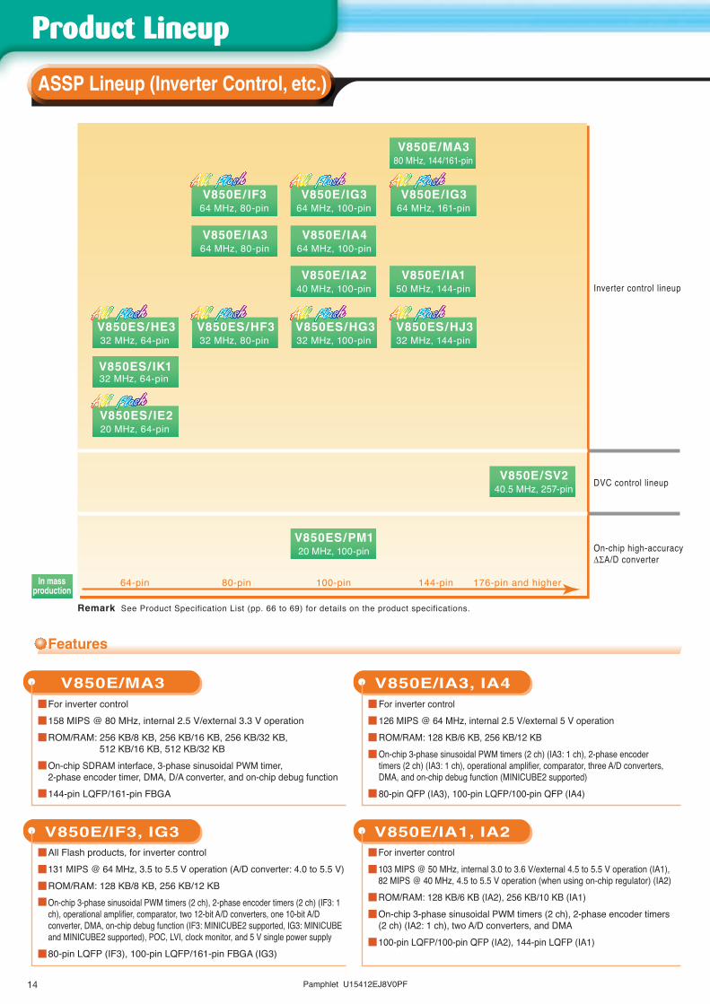
Remark See Product Specification List (pp. 66 to 69) for details on the product specifications.
Inverter control lineup
On-chip high-accuracy∆ΣA/D converter
DVC control lineup
V850E/IA3, IA4V850E/MA3
V850E/IF3, IG3
V850ES/PM120 MHz, 100-pin
V850E/SV240.5 MHz, 257-pin
V850E/ IA364 MHz, 80-pin
V850E/ IA464 MHz, 100-pin
V850E/MA380 MHz, 144/161-pin
V850E/ IG364 MHz, 100-pin
V850E/ IG364 MHz, 161-pin
V850E/ IF364 MHz, 80-pin
V850ES/ IK132 MHz, 64-pin
V850E/ IA240 MHz, 100-pin
V850E/ IA150 MHz, 144-pin
V850ES/ IE220 MHz, 64-pin
V850ES/HE332 MHz, 64-pin
V850ES/HF332 MHz, 80-pin
V850ES/HG332 MHz, 100-pin
V850ES/HJ332 MHz, 144-pin
Features
In massproduction
For inverter control158 MIPS @ 80 MHz, internal 2.5 V/external 3.3 V operationROM/RAM: 256 KB/8 KB, 256 KB/16 KB, 256 KB/32 KB,
512 KB/16 KB, 512 KB/32 KBOn-chip SDRAM interface, 3-phase sinusoidal PWM timer,2-phase encoder timer, DMA, D/A converter, and on-chip debug function144-pin LQFP/161-pin FBGA
All Flash products, for inverter control131 MIPS @ 64 MHz, 3.5 to 5.5 V operation (A/D converter: 4.0 to 5.5 V)ROM/RAM: 128 KB/8 KB, 256 KB/12 KBOn-chip 3-phase sinusoidal PWM timers (2 ch), 2-phase encoder timers (2 ch) (IF3: 1 ch), operational amplifier, comparator, two 12-bit A/D converters, one 10-bit A/D converter, DMA, on-chip debug function (IF3: MINICUBE2 supported, IG3: MINICUBE and MINICUBE2 supported), POC, LVI, clock monitor, and 5 V single power supply80-pin LQFP (IF3), 100-pin LQFP/161-pin FBGA (IG3)
For inverter control126 MIPS @ 64 MHz, internal 2.5 V/external 5 V operationROM/RAM: 128 KB/6 KB, 256 KB/12 KBOn-chip 3-phase sinusoidal PWM timers (2 ch) (IA3: 1 ch), 2-phase encoder timers (2 ch) (IA3: 1 ch), operational amplifier, comparator, three A/D converters,DMA, and on-chip debug function (MINICUBE2 supported)80-pin QFP (IA3), 100-pin LQFP/100-pin QFP (IA4)
64-pin 144-pin 176-pin and higher80-pin 100-pin
ASSP Lineup (Inverter Control, etc.)
V850E/SV2
Digital Video Camera
� 180˚ control for two motors
� DVC
Application examples
CCDdriver Camera DSP
processing
Audio & videoI/O interface
USB
SD memory, etc.
JPEGSDRAM
CCD
M
M
M
Moving pictureprocessing
DV processing IEEE1394
DV processingSDRAM
IEEE1394
JPEG field memory
USB2.0
JPEG CardInterface
MPEG-4
LCD panel
LCDcontroller
OSD
Head amplifier
Video head
Loading
Drum
CapstanMotor driver
(motor control)
MicMic
V850E/SV2
System controller & servo control microcontroller
S1 video input
A/D, CDS, SGC(camera pre-processing)
Camera DSPSDRAM
Lensdriver
System control/servo control block
Camera control block Still picture and moving picture processing block
V850E/ I F3 , IG3
180˚ Control for Two Motors
V850E/IG3 (100-pin/161-pin)V850E/IF3 (80-pin)
PFCAC
H level
L level
12-bit A/D
6ch
1ch
PFC AC
H level
L level
12-bit A/D
6ch
3ch3ch
SIO0etc.
6ch
UART22ch
I2C2ch
CSI23ch10-bit A/D
8ch
TOB0T1-T3TOB0B1-B3
TOB0OFF
TOB1T1-T3TOB1B1-B3
TOB1OFF
TOA21
TOA2OFFTOA3OFF
TOA31
BLDC BLDC
RESET-IC
Op-amp
Comparator
Regulator
Sensor
Sub microcontroller
EEPROMTM
Output of internalinformation
PG-FP5MINICUBEMINICUBE2
ON/OFF ON/OFF
ON/OFF ON/OFF
1 shunt3 shunts
180˚ control180˚ control
IPM IPM
V850ES/HE3, HF3, HG3, HJ3

Pamphlet U15412EJ8V0PF 1�
Product Lineup
V850E/SV2For camcorders (including DVCs)83 MIPS @ 40.5 MHz, internal 2.3 to 2.7 V/external 2.7 to 3.6 V operationROM/RAM: 512 KB/24 KBOn-chip 32-bit servo timer, boundary scan function, DMA,and on-chip debug function257-pin FBGA
V850E/IA1, IA2For inverter control103 MIPS @ 50 MHz, internal 3.0 to 3.6 V/external 4.5 to 5.5 V operation (IA1),82 MIPS @ 40 MHz, 4.5 to 5.5 V operation (when using on-chip regulator) (IA2)ROM/RAM: 128 KB/6 KB (IA2), 256 KB/10 KB (IA1)On-chip 3-phase sinusoidal PWM timers (2 ch), 2-phase encoder timers(2 ch) (IA2: 1 ch), two A/D converters, and DMA100-pin LQFP/100-pin QFP (IA2), 144-pin LQFP (IA1)
V850ES/IE2All Flash products, for inverter control39 MIPS @ 20 MHz, 3.5 to 5.5 V operation (A/D converter: 4.5 to 5.5 V)ROM/RAM: 64 KB/6 KB, 128 KB/6 KBOn-chip 3-phase sinusoidal PWM timer, two A/D converters, POC, LVI, and clock monitorOn-chip debug function (MINICUBE2 supported)64-pin LQFP
V850ES/IK1For inverter control63 MIPS @ 32 MHz, 3.5 to 5.5 V operation (A/D converter: 4.5 to 5.5 V)ROM/RAM: 64 KB/4 KB, 128 KB/6 KBOn-chip 3-phase sinusoidal PWM timer, two A/D converters, POC, LVI, and clock monitorOn-chip debug function (MINICUBE2 supported)64-pin LQFP
All Flash products69 MIPS @ 32 MHz, 66 MIPS @ 32 MHz (µPD70F3757 only), 3.7 to 5.5 V operation (A/D converter: 4.0 to 5.5 V)ROM/RAM: 128 KB/8 KB to 512 KB/32 KBOn-chip 3-phase sinusoidal PWM timer, multi-channel A/D converter, POC, LVI, DMA, on-chip debug function, motor control function, and SSCG*64-pin LQFP (HE3), 80-pin LQFP (HF3), 100-pin LQFP (HG3), 144-pin LQFP (HJ3)*Spread Spectrum Frequency Synthesizer Clock Generator
V850ES/PM1
For power meter control43 MIPS @ 20 MHz, 2.2 to 3.6 V operationROM/RAM: ROMless/10 KB, 128 KB/10 KBOn-chip high-accuracy 16-bit ∆ΣA/D converter, real-time counter100-pin LQFP
Remark See Product Specification List (pp. 66 to 69) for details on the product specifications.
Inverter control lineup
On-chip high-accuracy∆ΣA/D converter
DVC control lineup
V850E/IA3, IA4V850E/MA3
V850E/IF3, IG3
V850ES/PM120 MHz, 100-pin
V850E/SV240.5 MHz, 257-pin
V850E/ IA364 MHz, 80-pin
V850E/ IA464 MHz, 100-pin
V850E/MA380 MHz, 144/161-pin
V850E/ IG364 MHz, 100-pin
V850E/ IG364 MHz, 161-pin
V850E/ IF364 MHz, 80-pin
V850ES/ IK132 MHz, 64-pin
V850E/ IA240 MHz, 100-pin
V850E/ IA150 MHz, 144-pin
V850ES/ IE220 MHz, 64-pin
V850ES/HE332 MHz, 64-pin
V850ES/HF332 MHz, 80-pin
V850ES/HG332 MHz, 100-pin
V850ES/HJ332 MHz, 144-pin
Features
In massproduction
For inverter control158 MIPS @ 80 MHz, internal 2.5 V/external 3.3 V operationROM/RAM: 256 KB/8 KB, 256 KB/16 KB, 256 KB/32 KB,
512 KB/16 KB, 512 KB/32 KBOn-chip SDRAM interface, 3-phase sinusoidal PWM timer,2-phase encoder timer, DMA, D/A converter, and on-chip debug function144-pin LQFP/161-pin FBGA
All Flash products, for inverter control131 MIPS @ 64 MHz, 3.5 to 5.5 V operation (A/D converter: 4.0 to 5.5 V)ROM/RAM: 128 KB/8 KB, 256 KB/12 KBOn-chip 3-phase sinusoidal PWM timers (2 ch), 2-phase encoder timers (2 ch) (IF3: 1 ch), operational amplifier, comparator, two 12-bit A/D converters, one 10-bit A/D converter, DMA, on-chip debug function (IF3: MINICUBE2 supported, IG3: MINICUBE and MINICUBE2 supported), POC, LVI, clock monitor, and 5 V single power supply80-pin LQFP (IF3), 100-pin LQFP/161-pin FBGA (IG3)
For inverter control126 MIPS @ 64 MHz, internal 2.5 V/external 5 V operationROM/RAM: 128 KB/6 KB, 256 KB/12 KBOn-chip 3-phase sinusoidal PWM timers (2 ch) (IA3: 1 ch), 2-phase encoder timers (2 ch) (IA3: 1 ch), operational amplifier, comparator, three A/D converters,DMA, and on-chip debug function (MINICUBE2 supported)80-pin QFP (IA3), 100-pin LQFP/100-pin QFP (IA4)
64-pin 144-pin 176-pin and higher80-pin 100-pin
ASSP Lineup (Inverter Control, etc.)
V850E/SV2
Digital Video Camera
� 180˚ control for two motors
� DVC
Application examples
CCDdriver Camera DSP
processing
Audio & videoI/O interface
USB
SD memory, etc.
JPEGSDRAM
CCD
M
M
M
Moving pictureprocessing
DV processing IEEE1394
DV processingSDRAM
IEEE1394
JPEG field memory
USB2.0
JPEG CardInterface
MPEG-4
LCD panel
LCDcontroller
OSD
Head amplifier
Video head
Loading
Drum
CapstanMotor driver
(motor control)
MicMic
V850E/SV2
System controller & servo control microcontroller
S1 video input
A/D, CDS, SGC(camera pre-processing)
Camera DSPSDRAM
Lensdriver
System control/servo control block
Camera control block Still picture and moving picture processing block
V850E/ I F3 , IG3
180˚ Control for Two Motors
V850E/IG3 (100-pin/161-pin)V850E/IF3 (80-pin)
PFCAC
H level
L level
12-bit A/D
6ch
1ch
PFC AC
H level
L level
12-bit A/D
6ch
3ch3ch
SIO0etc.
6ch
UART22ch
I2C2ch
CSI23ch10-bit A/D
8ch
TOB0T1-T3TOB0B1-B3
TOB0OFF
TOB1T1-T3TOB1B1-B3
TOB1OFF
TOA21
TOA2OFFTOA3OFF
TOA31
BLDC BLDC
RESET-IC
Op-amp
Comparator
Regulator
Sensor
Sub microcontroller
EEPROMTM
Output of internalinformation
PG-FP5MINICUBEMINICUBE2
ON/OFF ON/OFF
ON/OFF ON/OFF
1 shunt3 shunts
180˚ control180˚ control
IPM IPM
V850ES/HE3, HF3, HG3, HJ3

1� Pamphlet U15412EJ8V0PF
Product Lineup
Features
V850ES/FE3, FF3, FG3, FJ3, FK3
All Flash products, for automotive electronics (body control applications)98 MIPS @ 48 MHz, 69 MIPS @ 32 MHz,3.3 to 5.5 V operation (A/D converter: 4.0 to 5.5 V)ROM/RAM: 128 KB/8 KB to 1024 KB/60 KBOn-chip aFCAN (5 ch max.) and LIN-compatible UART (8 ch max.)On-chip multi-channel A/D converter, motor control function,POC, LVI, clock monitor, DMA, on-chip debug function, and SSCG*64-pin LQFP (FE3), 80-pin LQFP (FF3), 100-pin LQFP (FG3),144-pin LQFP (FJ3), 176-pin LQFP (FK3)*Spread Spectrum Frequency Synthesizer Clock Generator
V850E/DG3, DJ3, DL3
All Flash products, for automotive electronics (dashboard control applications)126 MIPS @ 64 MHz (DJ3, DL3), 69 MIPS @ 32 MHz (DJ3), 34 MIPS @16 MHz (DG3),3.2 to 5.5 V operation (A/D converter: 3.5 to 5.5 V)ROM/RAM: 128 KB/6 KB to 2048 KB/84 KBOn-chip aFCAN (2 ch max.) and LIN-compatible UART (2 ch)On-chip meter driver, voltage comparator (DJ3, DL3 only), sound generator, POC, clock monitor, DMA (DJ3, DL3 only), and SSCG*100-pin LQFP (DG3), 144-pin LQFP (DJ3), 208-pin LQFP (DL3)*Spread Spectrum Frequency Synthesizer Clock Generator
V850ES/FE2, FF2, FG2, FJ2
For automotive electronics (body control applications)43 MIPS @ 20 MHz, 3.5 to 5.5 V operation (A/D converter: 4.0 to 5.5 V)ROM/RAM: 64 KB/4 KB to 512 KB/20 KBOn-chip aFCAN (4 ch max.) and LIN-compatible UART (4 ch max.)On-chip multi-channel A/D converter, POC, LVI, DMA, andon-chip debug function64-pin LQFP (FE2), 80-pin TQFP (FF2), 100-pin LQFP (FG2),144-pin LQFP (FJ2)
All Flash products, for automotive electronics (body control applications)43 MIPS @ 20 MHz, 3.3 to 5.5 V operation (A/D converter: 4.0 to 5.5 V)ROM/RAM: 64 KB/6 KB to 256 KB/16 KBOn-chip aFCAN (1 ch) and LIN-compatible UART (3 ch max.)On-chip multi-channel A/D converter, POC, LVI, clock monitor, and on-chip debug function64-pin LQFP (FE3-L), 80-pin LQFP (FF3-L), 100-pin LQFP (FG3-L)
V850E/IA1
For automotive electronics (body control applications)103 MIPS @ 50 MHz, internal 3.0 to 3.6 V/external 4.5 to 5.5 V operationROM/RAM: 256 KB/10 KBOn-chip FCAN (1 ch)On-chip 3-phase sinusoidal PWM timer, 2-phase encoder timer, two A/D converters, and DMA144-pin LQFP
V850/SC3
For car infotainment systems23 MIPS @ 20 MHz, 3.5 to 5.5 V operation (flash memory version:4.0 to 5.5 V, A/D converter: 4.5 to 5.5 V)ROM/RAM: 512 KB/24 KBOn-chip aFCAN (2 ch max.) and DMA (for internal units)144-pin LQFP
V850ES/SG3, SJ3
All Flash products, for car infotainment systems69 MIPS @ 32 MHz, 2.85 to 3.6 V operation (A/D converter: 3.0 to 3.6 V)ROM/RAM: 256 KB/24 KB to 1024 KB/60 KBOn-chip aFCAN (2 ch max.), LIN-compatible UART (4 ch max.), IEBus (1 ch), multi-channel serial interface, LVI, clock monitor,CRC, DMA, and on-chip debug function5 V withstand-voltage ports incorporated, and 5 V output is possibleby setting N-ch open-drain output100-pin LQFP (SG3), 144-pin LQFP (SJ3)
V850ES/SG2, SJ2
For car infotainment systems43 MIPS @ 20 MHz, 2.85 to 3.6 V operation (A/D converter: 3.0 to 3.6 V)ROM/RAM: 256 KB/24 KB, 384 KB/32 KB, 512 KB/40 KB, 640 KB/48 KBOn-chip aFCAN (2 ch max.), LIN-compatible UART (4 ch max.), multi-channel serial interface, LVI, clock monitor, CRC, DMA, and on-chip debug function5 V withstand-voltage ports incorporated, and 5 V output is possibleby setting N-ch open-drain output100-pin LQFP (SG2), 144-pin LQFP (SJ2)
V850ES/SG1
For car infotainment systems43 MIPS @ 20 MHz, 2.85 to 3.6 V operation (A/D converter: 3.0 to 3.6 V)ROM/RAM: 128 KB/8 KBOn-chip aFCAN (1 ch), clock monitor, and DMA5 V withstand-voltage ports incorporated, and 5 V output is possibleby setting N-ch open-drain output100-pin LQFP
3 V operation lineup
5 V operation lineup
Dashboard control
Remark See Product Specification List (pp. 70 to 78) for details on the product specifications.
In massproduction
Underdevelopment
For car infotainment systems66 MIPS @ 32 MHz, 3.0 to 3.6 V operationROM/RAM: 512 KB/40 KB, 640 KB/48 KBOn-chip aFCAN (2 ch max.), LIN-compatible UART (4 ch max.), multi-channel serial interface, clock monitor, CRC, DMA, and on-chip debug function5 V withstand-voltage ports incorporated, and 5 V output is possible by setting N-ch open-drain output100-pin LQFP (SG2-H), 144-pin LQFP (SJ2-H)
V850ES/SG2-H, SJ2-H
V850ES/SG2-H32 MHz, 100-pin
V850ES/SJ2-H32 MHz, 144-pin
V850ES/SG220 MHz, 100-pin
V850ES/SJ220 MHz, 144-pin
V850ES/SG120 MHz, 100-pin
V850E/IA150 MHz, 144-pin
V850/SC320 MHz, 144-pin
V850ES/FE220 MHz, 64-pin
V850ES/FF220 MHz, 80-pin
V850ES/FG220 MHz, 100-pin
V850ES/FJ220 MHz, 144-pin
V850E/DG316 MHz, 100-pin
V850ES/FE332 MHz, 64-pin
V850ES/FE3-L20 MHz, 64-pin
V850ES/FF3-L20 MHz, 80-pin
V850ES/FG3-L20 MHz, 100-pin
V850ES/SG332 MHz, 100-pin
V850ES/SJ332 MHz, 144-pin
V850E/SK3-H48 MHz, 176-pin
V850E/SJ3-H48 MHz, 144-pin
V850ES/JG3-H48 MHz, 100-pin
V850ES/JH3-H48 MHz, 128-pin
V850ES/FF332 MHz, 80-pin
V850ES/FG348 MHz/32 MHz, 100-pin
V850ES/FJ348 MHz/32 MHz, 144-pin
V850ES/FK348 MHz, 176-pin
V850E/DJ364 MHz/32 MHz, 144-pin
V850E/DL364 MHz, 208-pin
64-pin 80-pin 100-pin 144-pin 176-pin and higher
All flash products, for car infotainment systems95 MIPS @ 48 MHz, 2.85 to 3.6 V operation (A/D converter: 3.0 to 3.6 V)ROM/RAM: 1280 KB/92 KB* (SJ3-H only), 1536 KB/92 KB* On-chip aFCAN (2 ch max.), UART (8 ch max. (including two UART channelswith FIFO buffers)), IEBus (1 ch), multi-channel serial interface, LVI, clock monitor, CRC, DMA, real-time counter, SSCG**, and on-chip debug function5 V withstand-voltage ports incorporated, and 5 V output is possibleby setting N-ch open-drain output144-pin LQFP (SJ3-H), 176-pin LQFP (SK3-H)* 32 KB of expanded internal RAM included.
** Spread Spectrum Frequency Synthesizer Clock Generator
V850E/SJ3-H, SK3-H
All flash products, for general-purpose applications98 MIPS @ 48 MHz, 2.85 to 3.6 V operation (A/D converter, USB controller: 3.0 to 3.6 V)ROM/RAM: 256 KB/40 KB*On-chip aFCAN (1 ch) and LIN-compatible UART (5 ch max.)USB controller: USB 2.0 function (full-speed) × 1 ch100-pin LQFP (JG3-H), 128-pin LQFP (JH3-H)* 8 KB of data-only RAM included.
V850ES/JG3-H, JH3-H
ASSP Lineup (CAN)
V850ES/FE3-L, FF3-L, FG3-L

Pamphlet U15412EJ8V0PF 1�
Product Lineup
Features
V850ES/FE3, FF3, FG3, FJ3, FK3
All Flash products, for automotive electronics (body control applications)98 MIPS @ 48 MHz, 69 MIPS @ 32 MHz,3.3 to 5.5 V operation (A/D converter: 4.0 to 5.5 V)ROM/RAM: 128 KB/8 KB to 1024 KB/60 KBOn-chip aFCAN (5 ch max.) and LIN-compatible UART (8 ch max.)On-chip multi-channel A/D converter, motor control function,POC, LVI, clock monitor, DMA, on-chip debug function, and SSCG*64-pin LQFP (FE3), 80-pin LQFP (FF3), 100-pin LQFP (FG3),144-pin LQFP (FJ3), 176-pin LQFP (FK3)*Spread Spectrum Frequency Synthesizer Clock Generator
V850E/DG3, DJ3, DL3
All Flash products, for automotive electronics (dashboard control applications)126 MIPS @ 64 MHz (DJ3, DL3), 69 MIPS @ 32 MHz (DJ3), 34 MIPS @16 MHz (DG3),3.2 to 5.5 V operation (A/D converter: 3.5 to 5.5 V)ROM/RAM: 128 KB/6 KB to 2048 KB/84 KBOn-chip aFCAN (2 ch max.) and LIN-compatible UART (2 ch)On-chip meter driver, voltage comparator (DJ3, DL3 only), sound generator, POC, clock monitor, DMA (DJ3, DL3 only), and SSCG*100-pin LQFP (DG3), 144-pin LQFP (DJ3), 208-pin LQFP (DL3)*Spread Spectrum Frequency Synthesizer Clock Generator
V850ES/FE2, FF2, FG2, FJ2
For automotive electronics (body control applications)43 MIPS @ 20 MHz, 3.5 to 5.5 V operation (A/D converter: 4.0 to 5.5 V)ROM/RAM: 64 KB/4 KB to 512 KB/20 KBOn-chip aFCAN (4 ch max.) and LIN-compatible UART (4 ch max.)On-chip multi-channel A/D converter, POC, LVI, DMA, andon-chip debug function64-pin LQFP (FE2), 80-pin TQFP (FF2), 100-pin LQFP (FG2),144-pin LQFP (FJ2)
All Flash products, for automotive electronics (body control applications)43 MIPS @ 20 MHz, 3.3 to 5.5 V operation (A/D converter: 4.0 to 5.5 V)ROM/RAM: 64 KB/6 KB to 256 KB/16 KBOn-chip aFCAN (1 ch) and LIN-compatible UART (3 ch max.)On-chip multi-channel A/D converter, POC, LVI, clock monitor, and on-chip debug function64-pin LQFP (FE3-L), 80-pin LQFP (FF3-L), 100-pin LQFP (FG3-L)
V850E/IA1
For automotive electronics (body control applications)103 MIPS @ 50 MHz, internal 3.0 to 3.6 V/external 4.5 to 5.5 V operationROM/RAM: 256 KB/10 KBOn-chip FCAN (1 ch)On-chip 3-phase sinusoidal PWM timer, 2-phase encoder timer, two A/D converters, and DMA144-pin LQFP
V850/SC3
For car infotainment systems23 MIPS @ 20 MHz, 3.5 to 5.5 V operation (flash memory version:4.0 to 5.5 V, A/D converter: 4.5 to 5.5 V)ROM/RAM: 512 KB/24 KBOn-chip aFCAN (2 ch max.) and DMA (for internal units)144-pin LQFP
V850ES/SG3, SJ3
All Flash products, for car infotainment systems69 MIPS @ 32 MHz, 2.85 to 3.6 V operation (A/D converter: 3.0 to 3.6 V)ROM/RAM: 256 KB/24 KB to 1024 KB/60 KBOn-chip aFCAN (2 ch max.), LIN-compatible UART (4 ch max.), IEBus (1 ch), multi-channel serial interface, LVI, clock monitor,CRC, DMA, and on-chip debug function5 V withstand-voltage ports incorporated, and 5 V output is possibleby setting N-ch open-drain output100-pin LQFP (SG3), 144-pin LQFP (SJ3)
V850ES/SG2, SJ2
For car infotainment systems43 MIPS @ 20 MHz, 2.85 to 3.6 V operation (A/D converter: 3.0 to 3.6 V)ROM/RAM: 256 KB/24 KB, 384 KB/32 KB, 512 KB/40 KB, 640 KB/48 KBOn-chip aFCAN (2 ch max.), LIN-compatible UART (4 ch max.), multi-channel serial interface, LVI, clock monitor, CRC, DMA, and on-chip debug function5 V withstand-voltage ports incorporated, and 5 V output is possibleby setting N-ch open-drain output100-pin LQFP (SG2), 144-pin LQFP (SJ2)
V850ES/SG1
For car infotainment systems43 MIPS @ 20 MHz, 2.85 to 3.6 V operation (A/D converter: 3.0 to 3.6 V)ROM/RAM: 128 KB/8 KBOn-chip aFCAN (1 ch), clock monitor, and DMA5 V withstand-voltage ports incorporated, and 5 V output is possibleby setting N-ch open-drain output100-pin LQFP
3 V operation lineup
5 V operation lineup
Dashboard control
Remark See Product Specification List (pp. 70 to 78) for details on the product specifications.
In massproduction
Underdevelopment
For car infotainment systems66 MIPS @ 32 MHz, 3.0 to 3.6 V operationROM/RAM: 512 KB/40 KB, 640 KB/48 KBOn-chip aFCAN (2 ch max.), LIN-compatible UART (4 ch max.), multi-channel serial interface, clock monitor, CRC, DMA, and on-chip debug function5 V withstand-voltage ports incorporated, and 5 V output is possible by setting N-ch open-drain output100-pin LQFP (SG2-H), 144-pin LQFP (SJ2-H)
V850ES/SG2-H, SJ2-H
V850ES/SG2-H32 MHz, 100-pin
V850ES/SJ2-H32 MHz, 144-pin
V850ES/SG220 MHz, 100-pin
V850ES/SJ220 MHz, 144-pin
V850ES/SG120 MHz, 100-pin
V850E/IA150 MHz, 144-pin
V850/SC320 MHz, 144-pin
V850ES/FE220 MHz, 64-pin
V850ES/FF220 MHz, 80-pin
V850ES/FG220 MHz, 100-pin
V850ES/FJ220 MHz, 144-pin
V850E/DG316 MHz, 100-pin
V850ES/FE332 MHz, 64-pin
V850ES/FE3-L20 MHz, 64-pin
V850ES/FF3-L20 MHz, 80-pin
V850ES/FG3-L20 MHz, 100-pin
V850ES/SG332 MHz, 100-pin
V850ES/SJ332 MHz, 144-pin
V850E/SK3-H48 MHz, 176-pin
V850E/SJ3-H48 MHz, 144-pin
V850ES/JG3-H48 MHz, 100-pin
V850ES/JH3-H48 MHz, 128-pin
V850ES/FF332 MHz, 80-pin
V850ES/FG348 MHz/32 MHz, 100-pin
V850ES/FJ348 MHz/32 MHz, 144-pin
V850ES/FK348 MHz, 176-pin
V850E/DJ364 MHz/32 MHz, 144-pin
V850E/DL364 MHz, 208-pin
64-pin 80-pin 100-pin 144-pin 176-pin and higher
All flash products, for car infotainment systems95 MIPS @ 48 MHz, 2.85 to 3.6 V operation (A/D converter: 3.0 to 3.6 V)ROM/RAM: 1280 KB/92 KB* (SJ3-H only), 1536 KB/92 KB* On-chip aFCAN (2 ch max.), UART (8 ch max. (including two UART channelswith FIFO buffers)), IEBus (1 ch), multi-channel serial interface, LVI, clock monitor, CRC, DMA, real-time counter, SSCG**, and on-chip debug function5 V withstand-voltage ports incorporated, and 5 V output is possibleby setting N-ch open-drain output144-pin LQFP (SJ3-H), 176-pin LQFP (SK3-H)* 32 KB of expanded internal RAM included.
** Spread Spectrum Frequency Synthesizer Clock Generator
V850E/SJ3-H, SK3-H
All flash products, for general-purpose applications98 MIPS @ 48 MHz, 2.85 to 3.6 V operation (A/D converter, USB controller: 3.0 to 3.6 V)ROM/RAM: 256 KB/40 KB*On-chip aFCAN (1 ch) and LIN-compatible UART (5 ch max.)USB controller: USB 2.0 function (full-speed) × 1 ch100-pin LQFP (JG3-H), 128-pin LQFP (JH3-H)* 8 KB of data-only RAM included.
V850ES/JG3-H, JH3-H
ASSP Lineup (CAN)
V850ES/FE3-L, FF3-L, FG3-L

1� Pamphlet U15412EJ8V0PF
V850ES/SG3, SJ3
3 V operation lineup
5 V operation lineup
Remark See Product Specification List (pp.79 to 83) for details on the product specifications.
Product Lineup
V850ES/SG2-H32 MHz, 100-pin
V850ES/SJ2-H32 MHz, 144-pin
V850ES/SG220 MHz, 100-pin
V850ES/SJ220 MHz, 144-pin
V850ES/SG120 MHz, 100-pin
V850/SB219 MHz, 100-pin
V850/SC219 MHz, 144-pin
V850ES/SG332 MHz, 100-pin
V850ES/SJ332 MHz, 144-pin
V850E/SK3-H48 MHz, 176-pin
V850E/SJ3-H48 MHz, 144-pin
In massproduction
Features
All Flash products, for car infotainment systems69 MIPS @ 32 MHz, 2.85 to 3.6 V operation (A/D converter: 3.0 to 3.6 V)ROM/RAM: 256 KB/24 KB to 1024 KB/60 KBOn-chip LIN-compatible UART (4 ch max.), IEBus (1 ch), multi-channel serial interface, LVI, clock monitor, CRC, DMA, and on-chip debug function5 V withstand-voltage ports incorporated, and 5 V output is possible by setting N-ch open-drain output100-pin LQFP (SG3), 144-pin LQFP (SJ3)
V850E/SJ3-H, SK3-H
All flash products, for car infotainment systems95 MIPS @ 48 MHz, 2.85 to 3.6 V operation (A/D converter: 3.0 to 3.6 V)ROM/RAM: 1280 KB/92 KB* (SJ3-H only), 1536 KB/92 KB* On-chip UART (8 ch max. (including two UART channels with FIFO)), IEBus (1 ch), multi-channel serial interface, LVI, clock monitor, CRC, DMA, real-time counter, SSCG**, and on-chip debug function5 V withstand-voltage ports incorporated, and 5 V output is possibleby setting N-ch open-drain output144-pin LQFP (SJ3-H), 176-pin LQFP (SK3-H)* 32 KB of expanded internal RAM included.
** Spread Spectrum Frequency Synthesizer Clock Generator
V850ES/SG2-H, SJ2-H
For car infotainment systems66 MIPS @ 32 MHz, 3.0 to 3.6 V operationROM/RAM: 512 KB/40 KB, 640 KB/48 KBOn-chip LIN-compatible UART (4 ch max.), IEBus (1 ch), multi-channel serial interface, clock monitor, CRC, DMA, and on-chip debug function5 V withstand-voltage ports incorporated, and 5 V output is possible by setting N-ch open-drain output100-pin LQFP (SG2-H), 144-pin LQFP (SJ2-H)
V850ES/SG1
For car infotainment systems43 MIPS @ 20 MHz, 2.85 to 3.6 V operation (A/D converter: 3.0 to 3.6 V)ROM/RAM: 256 KB/12 KBOn-chip IEBus (1 ch) and clock monitor5 V withstand-voltage ports incorporated, and 5 V output is possible by setting N-ch open-drain output100-pin LQFP, 100-pin QFP
V850ES/SG2, SJ2
For car infotainment systems43 MIPS @ 20 MHz, 2.85 to 3.6 V operation (A/D converter: 3.0 to 3.6 V)ROM/RAM: 256 KB/24 KB, 384 KB/32 KB, 512 KB/40 KB, 640 KB/48 KBOn-chip LIN-compatible UART (4 ch max.), IEBus (1 ch), multi-channel serial interface, LVI, clock monitor, CRC, DMA, and on-chip debug function5 V withstand-voltage ports incorporated, and 5 V output is possible by setting N-ch open-drain output100-pin LQFP (SG2), 100-pin QFP (SG2 (ROM: 256 KB/384 KB versions only)), 144-pin LQFP (SJ2)
V850/SB2
For car infotainment systems22 MIPS @ 19 MHz, 15 MIPS @ 13 MHz, 4.0 to 5.5 V operation(A/D converter: 4.5 to 5.5 V)ROM/RAM: 128 KB/8 KB (13 MHz version), 256 KB/16 KB (13 MHz version), 384 KB/24 KB (19 MHz version), 512 KB/24 KB (19 MHz version)On-chip IEBus (1 ch) and DMA (for internal units)100-pin LQFP (ROM: 128 KB, 256 KB, 384 KB versions only)/100-pin QFP
V850/SC2
For car infotainment systems22 MIPS @ 19 MHz, 3.5 to 5.5 V operation (flash memory version: 4.0 to 5.5 V, A/D converter: 4.5 to 5.5 V)ROM/RAM: 512 KB/24 KBOn-chip IEBus (1 ch) and DMA (for internal units)144-pin LQFP
V850ES/SG3
Car Audio
� Car audio
4-/8-gradationLCD
Control system signal
Speaker
KEY
CD unit
Antenna
ASSP for CDµPD63763
PLLTuner unit
MPX Audio DSP (or electrical volume)
Microcontroller(CD control)
RF
DAC
servoDSP
MP3, WMA playback
MD unitCAN, IEBus
driver
Power detection IC
Inter-automobile communication (CAN, IEBus...)CD (MD)changer unit
V850ES/Sx3,V850E/Sx3-H
Driver
Microcontroller(CD control)
V850ES/Sx3,V850E/Sx3-H
Microcontroller (display/key control)78K0R, V850ES/Sx3,
V850E/Sx3-H
Poweramplifier
Battery(always ON)ACC(ON when engine is ON)
Regulator
Driver
Power block
Display unit
Application examples
Audio system signal
64-pin 80-pin 100-pin 144-pin 176-pin and higher
Underdevelopment
ASSP Lineup (IEBusTM)
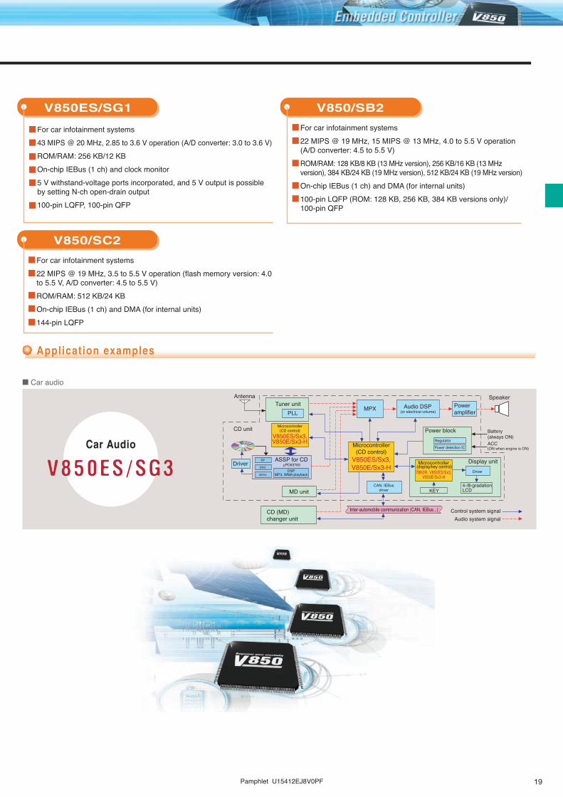
Pamphlet U15412EJ8V0PF 1�
V850ES/SG3, SJ3
3 V operation lineup
5 V operation lineup
Remark See Product Specification List (pp.79 to 83) for details on the product specifications.
Product Lineup
V850ES/SG2-H32 MHz, 100-pin
V850ES/SJ2-H32 MHz, 144-pin
V850ES/SG220 MHz, 100-pin
V850ES/SJ220 MHz, 144-pin
V850ES/SG120 MHz, 100-pin
V850/SB219 MHz, 100-pin
V850/SC219 MHz, 144-pin
V850ES/SG332 MHz, 100-pin
V850ES/SJ332 MHz, 144-pin
V850E/SK3-H48 MHz, 176-pin
V850E/SJ3-H48 MHz, 144-pin
In massproduction
Features
All Flash products, for car infotainment systems69 MIPS @ 32 MHz, 2.85 to 3.6 V operation (A/D converter: 3.0 to 3.6 V)ROM/RAM: 256 KB/24 KB to 1024 KB/60 KBOn-chip LIN-compatible UART (4 ch max.), IEBus (1 ch), multi-channel serial interface, LVI, clock monitor, CRC, DMA, and on-chip debug function5 V withstand-voltage ports incorporated, and 5 V output is possible by setting N-ch open-drain output100-pin LQFP (SG3), 144-pin LQFP (SJ3)
V850E/SJ3-H, SK3-H
All flash products, for car infotainment systems95 MIPS @ 48 MHz, 2.85 to 3.6 V operation (A/D converter: 3.0 to 3.6 V)ROM/RAM: 1280 KB/92 KB* (SJ3-H only), 1536 KB/92 KB* On-chip UART (8 ch max. (including two UART channels with FIFO)), IEBus (1 ch), multi-channel serial interface, LVI, clock monitor, CRC, DMA, real-time counter, SSCG**, and on-chip debug function5 V withstand-voltage ports incorporated, and 5 V output is possibleby setting N-ch open-drain output144-pin LQFP (SJ3-H), 176-pin LQFP (SK3-H)* 32 KB of expanded internal RAM included.
** Spread Spectrum Frequency Synthesizer Clock Generator
V850ES/SG2-H, SJ2-H
For car infotainment systems66 MIPS @ 32 MHz, 3.0 to 3.6 V operationROM/RAM: 512 KB/40 KB, 640 KB/48 KBOn-chip LIN-compatible UART (4 ch max.), IEBus (1 ch), multi-channel serial interface, clock monitor, CRC, DMA, and on-chip debug function5 V withstand-voltage ports incorporated, and 5 V output is possible by setting N-ch open-drain output100-pin LQFP (SG2-H), 144-pin LQFP (SJ2-H)
V850ES/SG1
For car infotainment systems43 MIPS @ 20 MHz, 2.85 to 3.6 V operation (A/D converter: 3.0 to 3.6 V)ROM/RAM: 256 KB/12 KBOn-chip IEBus (1 ch) and clock monitor5 V withstand-voltage ports incorporated, and 5 V output is possible by setting N-ch open-drain output100-pin LQFP, 100-pin QFP
V850ES/SG2, SJ2
For car infotainment systems43 MIPS @ 20 MHz, 2.85 to 3.6 V operation (A/D converter: 3.0 to 3.6 V)ROM/RAM: 256 KB/24 KB, 384 KB/32 KB, 512 KB/40 KB, 640 KB/48 KBOn-chip LIN-compatible UART (4 ch max.), IEBus (1 ch), multi-channel serial interface, LVI, clock monitor, CRC, DMA, and on-chip debug function5 V withstand-voltage ports incorporated, and 5 V output is possible by setting N-ch open-drain output100-pin LQFP (SG2), 100-pin QFP (SG2 (ROM: 256 KB/384 KB versions only)), 144-pin LQFP (SJ2)
V850/SB2
For car infotainment systems22 MIPS @ 19 MHz, 15 MIPS @ 13 MHz, 4.0 to 5.5 V operation(A/D converter: 4.5 to 5.5 V)ROM/RAM: 128 KB/8 KB (13 MHz version), 256 KB/16 KB (13 MHz version), 384 KB/24 KB (19 MHz version), 512 KB/24 KB (19 MHz version)On-chip IEBus (1 ch) and DMA (for internal units)100-pin LQFP (ROM: 128 KB, 256 KB, 384 KB versions only)/100-pin QFP
V850/SC2
For car infotainment systems22 MIPS @ 19 MHz, 3.5 to 5.5 V operation (flash memory version: 4.0 to 5.5 V, A/D converter: 4.5 to 5.5 V)ROM/RAM: 512 KB/24 KBOn-chip IEBus (1 ch) and DMA (for internal units)144-pin LQFP
V850ES/SG3
Car Audio
� Car audio
4-/8-gradationLCD
Control system signal
Speaker
KEY
CD unit
Antenna
ASSP for CDµPD63763
PLLTuner unit
MPX Audio DSP (or electrical volume)
Microcontroller(CD control)
RF
DAC
servoDSP
MP3, WMA playback
MD unitCAN, IEBus
driver
Power detection IC
Inter-automobile communication (CAN, IEBus...)CD (MD)changer unit
V850ES/Sx3,V850E/Sx3-H
Driver
Microcontroller(CD control)
V850ES/Sx3,V850E/Sx3-H
Microcontroller (display/key control)78K0R, V850ES/Sx3,
V850E/Sx3-H
Poweramplifier
Battery(always ON)ACC(ON when engine is ON)
Regulator
Driver
Power block
Display unit
Application examples
Audio system signal
64-pin 80-pin 100-pin 144-pin 176-pin and higher
Underdevelopment
ASSP Lineup (IEBusTM)

�0 Pamphlet U15412EJ8V0PF
Product Lineup
Memory Lineup
ROM size (bytes)
640K
768K
1024K
512K
384K
376K
256K
192K
1280K
2048K
128K
96K
64K
ROMless
4K 24K 32K 40K 48K 56K 60K 84K 92KRAM size (bytes)
8K6K 10K 12K 16K 20K
Instruction RAM: 128 KB Instruction RAM: 168 KB
MA2
FE2
MA1IA1
MA3
JJ3JG3
SJ2SG2
SJ2-HSG2-H
SJ2SG2
SV2SC3SC2
SC1
SB2SB1
MS1
KE1+SA1V853
MA1MS2MS1 PM1 ME2 ST2
SA1IK1
V853
MS1
HE2 HF2IE2
MA1
KE2
FE3-LFF3-L
FE3-LFF3-L
SA1V853MA3
SA2
SG1FE3
JF3-L
JG3-L
HE3
MA1PM1
FF2
HJ2HG2HF2JJ2JG2
SG2MA3
ME3
KF1+
FG2FF2
FJ2
DJ3-32Note 2
FE3-L
DG3Note 1
SG1
SB2SB1FJ3-32Note 2
FG3-32Note 2
FF3-LFE3-L
JG3-LJF3-L
HJ3HG3HF3
FF3FE3
JG2JJ2
KG1+
SA2SA3
MA3
KG2KJ2
KJ1+
JJ3JG3
JG3-HNote 1, 3
JH3-HNote 1, 3
JG3-HNote 1, 3
JH3-HNote 1, 3
JG3-HNote 1, 3
JH3-HNote 1, 3
JG3-UNote 1, 3
JH3-UNote 1, 3
JG3-UNote 1, 3
JH3-UNote 1, 3
SJ3-HNote 1, 4
SK3-HNote 1, 4
SJ3-HNote 1, 4
SJ2 SG2SG2-HSJ2-H
MA3 HJ2FJ2
DJ3-32Note 2
FK3HJ3
FJ3-48Note 2
FG3-48Note 2SB2SB1
DJ3-64Note 2
FG2DJ3-32Note 2
FJ2HJ2
FG3-48Note 2
SG3
FJ3-48Note 2
SG3SJ3
SG3SJ3
JJ3
SJ3SG3
FK3
JG3
JG3
JJ3
DL3
SJ3
DJ3-64Note 2
SG3
FK3FJ3-48Note 2
FJ3-48Note 2DJ3-64Note 2
SG3SJ3
JG2JJ2
JG2
JG2JJ2
FE2
FG2
KG1+KF1+
FF2
DG3Note 1
IK1KG2
KJ1+
IA2
KJ2
IE2
IA3IA4
KF2
HE2
SB2SB1
FF3
IG3IF3
FE3-LFF3-LFG3-L
FG3-32Note 2
HG2HJ2
KF2
HF2
IA3
IG3
FG3-L
FF3-LFG3-L
IF3IA4
1536K
JJ2
Note 1. Under development Note 2. xx-32: 32 MHz version, xx-48: 48 MHz version, xx-64: 64MHz version Note 3. 8 KB of data-only RAM included.Note 4. 32 KB of expanded internal RAM included.
Flash memory version Mask ROM version Mask ROM/flash memory version

Pamphlet U15412EJ8V0PF �1
Product Lineup
Memory Lineup
ROM size (bytes)
640K
768K
1024K
512K
384K
376K
256K
192K
1280K
2048K
128K
96K
64K
ROMless
4K 24K 32K 40K 48K 56K 60K 84K 92KRAM size (bytes)
8K6K 10K 12K 16K 20K
Instruction RAM: 128 KB Instruction RAM: 168 KB
MA2
FE2
MA1IA1
MA3
JJ3JG3
SJ2SG2
SJ2-HSG2-H
SJ2SG2
SV2SC3SC2
SC1
SB2SB1
MS1
KE1+SA1V853
MA1MS2MS1 PM1 ME2 ST2
SA1IK1
V853
MS1
HE2 HF2IE2
MA1
KE2
FE3-LFF3-L
FE3-LFF3-L
SA1V853MA3
SA2
SG1FE3
JF3-L
JG3-L
HE3
MA1PM1
FF2
HJ2HG2HF2JJ2JG2
SG2MA3
ME3
KF1+
FG2FF2
FJ2
DJ3-32Note 2
FE3-L
DG3Note 1
SG1
SB2SB1FJ3-32Note 2
FG3-32Note 2
FF3-LFE3-L
JG3-LJF3-L
HJ3HG3HF3
FF3FE3
JG2JJ2
KG1+
SA2SA3
MA3
KG2KJ2
KJ1+
JJ3JG3
JG3-HNote 1, 3
JH3-HNote 1, 3
JG3-HNote 1, 3
JH3-HNote 1, 3
JG3-HNote 1, 3
JH3-HNote 1, 3
JG3-UNote 1, 3
JH3-UNote 1, 3
JG3-UNote 1, 3
JH3-UNote 1, 3
SJ3-HNote 1, 4
SK3-HNote 1, 4
SJ3-HNote 1, 4
SJ2 SG2SG2-HSJ2-H
MA3 HJ2FJ2
DJ3-32Note 2
FK3HJ3
FJ3-48Note 2
FG3-48Note 2SB2SB1
DJ3-64Note 2
FG2DJ3-32Note 2
FJ2HJ2
FG3-48Note 2
SG3
FJ3-48Note 2
SG3SJ3
SG3SJ3
JJ3
SJ3SG3
FK3
JG3
JG3
JJ3
DL3
SJ3
DJ3-64Note 2
SG3
FK3FJ3-48Note 2
FJ3-48Note 2DJ3-64Note 2
SG3SJ3
JG2JJ2
JG2
JG2JJ2
FE2
FG2
KG1+KF1+
FF2
DG3Note 1
IK1KG2
KJ1+
IA2
KJ2
IE2
IA3IA4
KF2
HE2
SB2SB1
FF3
IG3IF3
FE3-LFF3-LFG3-L
FG3-32Note 2
HG2HJ2
KF2
HF2
IA3
IG3
FG3-L
FF3-LFG3-L
IF3IA4
1536K
JJ2
Note 1. Under development Note 2. xx-32: 32 MHz version, xx-48: 48 MHz version, xx-64: 64MHz version Note 3. 8 KB of data-only RAM included.Note 4. 32 KB of expanded internal RAM included.
Flash memory version Mask ROM version Mask ROM/flash memory version

�� Pamphlet U15412EJ8V0PF
Product Lineup
No. of pinsTypeSizePitchThicknessMounted products
121 pinsFBGA (F1)12 × 12 mm0.8 mm1.13 mmSA1, SA3
No. of pinsTypeSizePitchThicknessMounted products
64 pinsLQFP (GB)10 × 10 mm0.5 mm1.4 mmKE1+, KE2, HE2, HE3,FE2, FE3, FE3-L
No. of pinsTypeSizePitchThicknessMounted products
161 pinsFBGA (F1)10 × 10 mm0.65 mm1.13 mmIG3
No. of pinsTypeSizePitchThicknessMounted products
64 pinsTQFP (GK)12 × 12 mm0.65 mm1.0 mmKE1+
No. of pinsTypeSizePitchThicknessMounted products
100 pinsLQFP (GC)14 × 14 mm0.5 mm1.4 mmKG1+, KG2, JG2, JG3, JG3-L, JG3-H, JG3-U, HG2,HG3, SA1, SB1, SB2, SG2, SG2-H, SG3, PM1, FG2,FG3, FG3-L, MS2, MA2, IA2, IA4, IG3, DG3, V853, SG1
No. of pinsTypeSizePitchThicknessMounted products
128 pinsLQFP (GF)14 × 20 mm0.5 mm1.4 mmJH3-H, JH3-U
No. of pinsTypeSizePitchThicknessMounted products
257 pinsFBGA (F1)14 × 14 mm0.65 mm1.13 mmSV2
No. of pinsTypeSizePitchThicknessMounted products
144 pinsLQFP (GJ)20 × 20 mm0.5 mm1.4 mmKJ1+, KJ2, JJ2, JJ3, HJ2, HJ3, SC1,SC2, SC3, SJ2, SJ2-H, SJ3, SJ3-H, ST2,FJ2, FJ3, MS1, MA1, MA3, IA1, DJ3
No. of pinsTypeSizePitchThicknessMounted products
80 pinsQFP (GC)14 × 14 mm0.65 mm1.4 mmKF1+, KF2, IA3
No. of pinsTypeSizePitchThicknessMounted products
80 pinsLQFP (GC)14 × 14 mm0.65 mm1.4 mmIF3, JF3-L
No. of pinsTypeSizePitchThicknessMounted products
176 pinsLQFP (GM)24 × 24 mm0.5 mm1.4 mmME2, FK3, SK3-H
No. of pinsTypeSizePitchThicknessMounted products
100 pinsTQFP (GC)14 × 14 mm0.5 mm1.0 mmSA2
No. of pinsTypeSizePitchThicknessMounted products
176 pinsQFP (GM)24 × 24 mm0.5 mm2.7 mmME3
No. of pinsTypeSizePitchThicknessMounted products
208 pinsQFP (GD)28 × 28 mm0.5 mm3.2 mmDL3
No. of pinsTypeSizePitchThicknessMounted products
80 pinsLQFP (GK)12 × 12 mm0.5 mm1.4 mmFF3, HF3, JF3-L, FF3-L
No. of pinsTypeSizePitchThicknessMounted products
161 pinsFBGA (F1)13 × 13 mm0.8 mm1.13 mmMA1, MA3
No. of pinsTypeSizePitchThicknessMounted products
100 pinsQFP (GF)14 × 20 mm0.65 mm2.7 mmKG1+, KG2, JG2, SB1,SB2, SG1, SG2, IA2, IA4
No. of pinsTypeSizePitchThicknessMounted products
120 pinsTQFP (GC)14 × 14 mm0.4 mm1.0 mmST2
No. of pinsTypeSizePitchThicknessMounted products
64 pinsLQFP (GC)14 × 14 mm0.8 mm1.4 mmIK1, IE2
No. of pinsTypeSizePitchThicknessMounted products
80 pinsTQFP (GK)12 × 12 mm0.5 mm1.0 mmKF1+, HF2, FF2
Package Lineup
No. of pinsTypeSizePitchThicknessMounted products
100 pinsLQFP (GF)14 × 20 mm0.65 mm1.4 mmIG3, JG3-L

Pamphlet U15412EJ8V0PF ��
Product Lineup
No. of pinsTypeSizePitchThicknessMounted products
121 pinsFBGA (F1)12 × 12 mm0.8 mm1.13 mmSA1, SA3
No. of pinsTypeSizePitchThicknessMounted products
64 pinsLQFP (GB)10 × 10 mm0.5 mm1.4 mmKE1+, KE2, HE2, HE3,FE2, FE3, FE3-L
No. of pinsTypeSizePitchThicknessMounted products
161 pinsFBGA (F1)10 × 10 mm0.65 mm1.13 mmIG3
No. of pinsTypeSizePitchThicknessMounted products
64 pinsTQFP (GK)12 × 12 mm0.65 mm1.0 mmKE1+
No. of pinsTypeSizePitchThicknessMounted products
100 pinsLQFP (GC)14 × 14 mm0.5 mm1.4 mmKG1+, KG2, JG2, JG3, JG3-L, JG3-H, JG3-U, HG2,HG3, SA1, SB1, SB2, SG2, SG2-H, SG3, PM1, FG2,FG3, FG3-L, MS2, MA2, IA2, IA4, IG3, DG3, V853, SG1
No. of pinsTypeSizePitchThicknessMounted products
128 pinsLQFP (GF)14 × 20 mm0.5 mm1.4 mmJH3-H, JH3-U
No. of pinsTypeSizePitchThicknessMounted products
257 pinsFBGA (F1)14 × 14 mm0.65 mm1.13 mmSV2
No. of pinsTypeSizePitchThicknessMounted products
144 pinsLQFP (GJ)20 × 20 mm0.5 mm1.4 mmKJ1+, KJ2, JJ2, JJ3, HJ2, HJ3, SC1,SC2, SC3, SJ2, SJ2-H, SJ3, SJ3-H, ST2,FJ2, FJ3, MS1, MA1, MA3, IA1, DJ3
No. of pinsTypeSizePitchThicknessMounted products
80 pinsQFP (GC)14 × 14 mm0.65 mm1.4 mmKF1+, KF2, IA3
No. of pinsTypeSizePitchThicknessMounted products
80 pinsLQFP (GC)14 × 14 mm0.65 mm1.4 mmIF3, JF3-L
No. of pinsTypeSizePitchThicknessMounted products
176 pinsLQFP (GM)24 × 24 mm0.5 mm1.4 mmME2, FK3, SK3-H
No. of pinsTypeSizePitchThicknessMounted products
100 pinsTQFP (GC)14 × 14 mm0.5 mm1.0 mmSA2
No. of pinsTypeSizePitchThicknessMounted products
176 pinsQFP (GM)24 × 24 mm0.5 mm2.7 mmME3
No. of pinsTypeSizePitchThicknessMounted products
208 pinsQFP (GD)28 × 28 mm0.5 mm3.2 mmDL3
No. of pinsTypeSizePitchThicknessMounted products
80 pinsLQFP (GK)12 × 12 mm0.5 mm1.4 mmFF3, HF3, JF3-L, FF3-L
No. of pinsTypeSizePitchThicknessMounted products
161 pinsFBGA (F1)13 × 13 mm0.8 mm1.13 mmMA1, MA3
No. of pinsTypeSizePitchThicknessMounted products
100 pinsQFP (GF)14 × 20 mm0.65 mm2.7 mmKG1+, KG2, JG2, SB1,SB2, SG1, SG2, IA2, IA4
No. of pinsTypeSizePitchThicknessMounted products
120 pinsTQFP (GC)14 × 14 mm0.4 mm1.0 mmST2
No. of pinsTypeSizePitchThicknessMounted products
64 pinsLQFP (GC)14 × 14 mm0.8 mm1.4 mmIK1, IE2
No. of pinsTypeSizePitchThicknessMounted products
80 pinsTQFP (GK)12 × 12 mm0.5 mm1.0 mmKF1+, HF2, FF2
Package Lineup
No. of pinsTypeSizePitchThicknessMounted products
100 pinsLQFP (GF)14 × 20 mm0.65 mm1.4 mmIG3, JG3-L
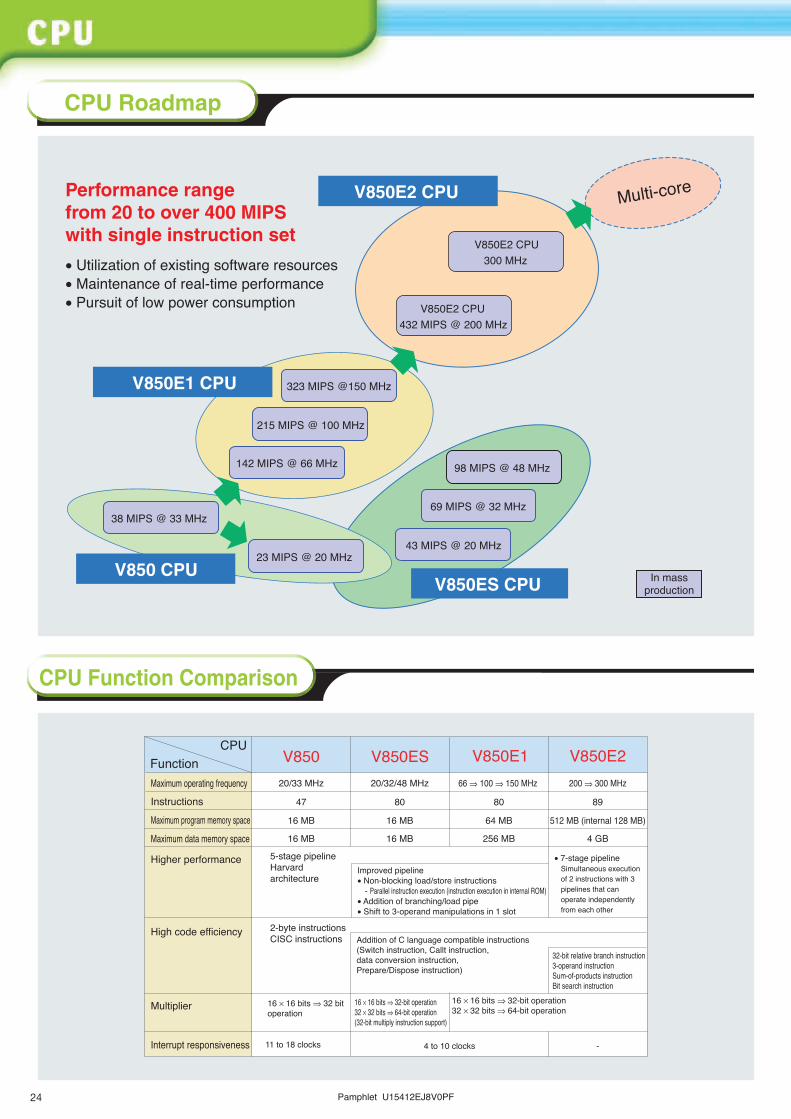
�� Pamphlet U15412EJ8V0PF
V850E2 CPU432 MIPS @ 200 MHz
V850E2 CPU300 MHz
38 MIPS @ 33 MHz
43 MIPS @ 20 MHz23 MIPS @ 20 MHz
142 MIPS @ 66 MHz
215 MIPS @ 100 MHz
V850 CPUV850ES CPU
V850E1 CPU
V850E2 CPU
323 MIPS @150 MHz
69 MIPS @ 32 MHz
98 MIPS @ 48 MHz
Multi-core
In massproduction
Performance rangefrom 20 to over 400 MIPSwith single instruction set
• Utilization of existing software resources• Maintenance of real-time performance• Pursuit of low power consumption
V850 V850E2FunctionCPU
Higher performance
High code efficiency
Multiplier
Interrupt responsiveness
5-stage pipeline Harvardarchitecture
2-byte instructions CISC instructions
Improved pipeline • Non-blocking load/store instructions
- Parallel instruction execution (instruction execution in internal ROM) • Addition of branching/load pipe • Shift to 3-operand manipulations in 1 slot
Addition of C language compatible instructions (Switch instruction, Callt instruction,data conversion instruction,Prepare/Dispose instruction)
32-bit relative branch instruction3-operand instructionSum-of-products instructionBit search instruction
16 × 16 bits ⇒ 32 bitoperation
16 × 16 bits ⇒ 32-bit operation 32 × 32 bits ⇒ 64-bit operation (32-bit multiply instruction support)
16 × 16 bits ⇒ 32-bit operation 32 × 32 bits ⇒ 64-bit operation
Maximum operating frequencyInstructions 47
20/33 MHz
16 MB
V850ES20/32/48 MHz
80
16 MB
V850E166 ⇒ 100 ⇒ 150 MHz
80
64 MBMaximum program memory space
200 ⇒ 300 MHz
89
512 MB (internal 128 MB)
4 to 10 clocks -11 to 18 clocks
• 7-stage pipelineSimultaneous execution of 2 instructions with 3 pipelines that can operate independently from each other
Maximum data memory space 16 MB 16 MB 256 MB 4 GB
CPU Roadmap
CPU Function Comparison

Pamphlet U15412EJ8V0PF ��
uUse of same development methods for standard V850 products, ASIC microcontrollers Quick market introduction of standard products System optimization through shift to system LSIs
uCPU development considering system LSIs Release of CPUs that support on-chip debugging 2-stage structure consisting of 32-bit sync system bus & 16-bit async peripheral function bus Large choice of peripheral function macros
uMany supported processes and large range of required performance, and power consumption
0.25 µm0.15 µm 0.13 µm 90 nm
65 nm
NPB: Peripheral I/O bus VSB: System bus iLB: Internal instruction bus dLB: Internal data bus
V850E2 system
TIMER
UART
PWM
PORT
CSI
etc ...
User circuit (UDL)
UDL1
UDL2
IP
RAM
External bus
Flashmemory SDRAM SRAM I/O
DMACNBA85E300
MEMCNBT85E535
NPB
INTCQL85E70x Arbiter
VSB
NBA85E2S
CPU
VSBI/F
NPBI/F
INTCI/F
Instructioncache
Datacache
RCU
JTAGIE
dLB
iLBInstructionmemory
Datamemory
JTAG
DCU
V850E2 system configuration example
System LSI Support
V850E1 system configuration example
V850E1 systemNPB: Peripheral I/O bus VSB: System bus VFB: Internal instruction bus VDB: Internal data bus
User circuit (UDL)
UDL1
UDL2
IP
RAM
MEMCNBT85E500
NPB
VSBVSBI/F
NPBI/F
DMAC
INTC
CPU
DCU
Flashmemory SRAM I/O
JTAG IE
JTAG
VDB
Cacheinterface
VFB
Instructioncache
Datamemory
Instructionmemory
External bus
NBU85ET TIMER
UART
PWM
PORT
CSI
etc ...

�� Pamphlet U15412EJ8V0PF
Harvard architectureThe V850 microcontrollers use Harvard architecture, which is designed so that the instruction bus and data bus can operate completely independently from each other, thereby preventing pipeline operation problems and ensuring efficient instruction execution.
WB
In the case of an architecture other than Harvard architecture, the MEM stage of instruction 1 and the IF stage of instruction 4, and the MEM stage of instruction 2 and the IF stage of instruction 5 conflict, causing bus waits. This in turn causes the pipeline operation to become disordered and lowers the instruction execution speed.
IF ID EX MEM
Instruction 1
Instruction 2
Instruction 3
Instruction 4
Instruction 5
---: Idles inserted due to bus wait
WBMEM
MEM
EX
WB
WB
EX
ID
---
---
MEM
ID
IF
WB
EX
---
MEM
---
IF
IDIF
IF ID EX
Pipeline Operation of Non-Harvard Architecture
CPU
Instruction bus
Data bus
Instructionfetch
Externalmemory
On-chipperipheral
I/O
Operanddata access
InternalRAM
InternalROM
BCU
5-stage pipeline processingThe V850 microcontrollers use a 5-stage pipeline structure (5 stages from instruction fetch to writeback) that supports simultaneous processing of 5 instructions, thus enabling the execution of almost all instructions in just one clock.
ID EX WB
ID EX
MEM
MEM WB
ID EX MEM WB
ID EX MEM WB
ID EX MEM WB
IF ID EX MEM WB
Instruction 1
Instruction 2
Instruction 3
Instruction 4
Instruction 5
Instruction 6
IF: Instruction fetchID: Instruction decodeEX: Instruction executionMEM: Memory access to target addressWB: Write execution result to register
Instruction 1completion
Instruction 2completion
Instruction 3completion
An instruction is executed in each clock
Instruction 4completion
Instruction 5completion
Instruction 6completion
Internal system clock
IF
IF
IF
IF
IF
V850 Common ArchitectureThe V850 microcontrollers are single-chip RISC microcontrollers that use an architecture optimized for embedding, and have the following features.
5-stage pipeline processing Harvard architecture 32 general-purpose registers Simple addressing
2-byte basic instruction set
32-bit barrel shifter
Support of CISC-like instructions Multi-status flags DSP function

Pamphlet U15412EJ8V0PF ��
General-purpose register configuration System register configuration
The number of registers can be selected from among 22, 26, and 32 as a compiler option to efficiently execute application programs. Unused registers can be used as a software register bank for which save and restore processing is not required during interrupt servicing or task switching, which increases the processing speed.
Software register bank
Register bankinterrupt
Programexecution
Programexecution
Interrupt servicinginstruction execution
Actual interruptservicing time
Normalinterrupt
Programexecution
Interrupt servicinginstruction execution
Programexecution
Actual interruptservicing time
User interrupt servicing routine execution time
Total interrupt servicing time
32 general-purpose registers The V850 microcontrollers have 32 general-purpose registers. Along with a hardware environment that is ideal for program execution, the development environment, including compilers, exploits these 32 registers to achieve program generation with superior code efficiency and execution performance.
0
1000
2000
3000
4000
0
3
6
9
12
Comparison of Performance/Object Efficiency According to Number of RegistersByte count (bytes) Execution time (s)
Number of registersUsed C program: Servo control module
16 18 20 22 24 26 28 30 32
Byte count Execution time
For example, looking at the program execution time and code size changes when the number of registers used by the compiler is changed using the servo control module, we can see that the larger the number of registers, the better the program execution speed and the smaller the code size. However, from about 26 registers, the improvement in terms of execution speed and code size becomes smaller, and in the neighborhood of 32 registers, there are no more changes. This is why the V850 microcontrollers have been provided with 32 registers as a strict minimum requirement.
Save the program counter, etc., to a save register. Execute the interrupt restore instruction. Restore the program counter value, etc., from the save register. Save general-purpose registers to stacks. Restore general-purpose registers from stacks.
Address/data variable register (If real-time OS being used does not use r2)
r031
31
Zero Registerr1r2r3r4r5r6r7r8r9r10r11r12r13r14r15r16r17r18r19
r21r22r23r24r25r26r27r28r29r30r31
r20
PC
Name
r0
r1
r2
r3
r4
r5
r6-r29
r30
r31
PC
Application Operation
Zero registerAssembler reservation
Always holds "0"
Stack pointer
Global pointer
Text pointer
Element pointer
Link pointer
Program counter
Used as working register for address generation
Used for stack frame generation during function callUsed when accessing globalvariables in the data areaUsed as register for specifyingthe beginning of the text area (program code allocation)
Address/data variable register
Used as base pointer for address generation during memory access Used during function call by compilerHolds instruction addresses during program execution
Reserved for Address Generation
Stack Pointer (SP)Global Pointer (GP)Text Pointer (TP)
Link Pointer (LP)Element Pointer (EP)
Program Counter
0
0
No.
0
1
2
3
4
5
16
17
18
19
20
6-15, 21-31
EIPC
EIPSW
FEPC
FEPSW
ECR
PSW
CTPC
CTPSW
DBPC
DBPSW
CTBP
Reserved
Application
Supported byother thanV850 CPU products
Register for saving status during interrupt
Register for saving status during NMI
Interrupt source register
Program status word
Register for saving status during CALLT execution
Register for saving status during exception/debug trap
CALLT base pointer
LDSR
×
×
STSR
×
×: Access prohibited
: Access enabled
LDSR: Instruction to load general-purpose register contents to system register
STSR: Instruction to store system register contents to general-purpose register
OperandSpecificationSystem
Register Name

�� Pamphlet U15412EJ8V0PF
The increased amount of address calculations in the CPU in the case of complex addressing causes disturbances in the pipeline operation. As a result, address calculation becomes a bottleneck for pipeline processing and raising the frequency to increase the performance becomes difficult. The V850 microcontrollers avoid this problem by supporting only simple addressing.
Simple addressing
The V850 microcontrollers employ a 2-byte instruction code to perform basic processing to enable compact program development equivalent to 16-bit CISC microcontrollers.
1.03
1.02
1.48
1.00
Object Code Size Comparison(Dhrystone 1.1/Large model)
16-bitV (CISC)
78K4 (CISC)
V850 (RISC)
VRTM/MIPSTM32 (RISC)
• Improved object efficiency through ROMization programming Application of 2-byte instructions to all basic processing, consisting of load, store, arithmetic/logic operations, and branching.
• To realize ease of use, restrictions on 16-bit fixed-length instructions are partially removed through incorporation of 32-bit instructions.
• Bit manipulation instructions, etc.
2-byte basic instruction set
l Operand addresses
reg1031
disp16016 1531
Signed extensionMemory subject to manipulation
reg1031
disp16016 1531
Signed extensionMemory subject to manipulation
• Register addressing Addressing that accesses the general-purpose register specified by the general-purpose specification field or a system register as an operand.
• Immediate addressing Addressing of 5-bit data or 16-bit data for manipulation in the instruction code.
• Based addressing Addressing that accesses memory, with the sum of the contents of the general-purpose register (reg1) and 16-bit displacement (disp16) as the operand address.
• Bit addressing Addressing that accesses 1 bit of 1 byte of the memory space, with the sum of the contents of the general-purpose reg is ter ( reg1) and 16-bit displacement (disp16) that has been sign extended to word length as the operand address.
l Instruction addresses
PC26 2531
0
022 2131Signed extension disp22
PC026 2531
0Memory subject to manipulation
0
reg1
PC026 2531
026 2531
0Memory subject to manipulation
• Register addressing (register indirect) Transfer the contents of the general-purpose register specified by the instruction (reg1) to the program counter (PC).
• Relative addressing (PC dependent) Add 9 signed bits or 22 signed bits of data of the instruction code to the program counter.
Addressing mode
Processing time Processing time
All processing is standardized and efficient
Pipeline processing sequence
Pipeline Processing Time and CPU Operating Frequency
Operating frequency he ld back by s l ow processing
In case of excessive addressing In case of simple addressing
Address calculation
Execution
Memory access
Writeback
Instruction fetch

Pamphlet U15412EJ8V0PF ��
The V850 microcontrollers support bit manipulation instructions suitable for flag manipulation on I/O registers, which play a large role in embedding control.
Object size
Execution time
Coding example
Item
4 bytes
4 clocks 4 clocks 8 clocks
When Used When Not Used
set1 6, ASIM00[r0] ld.b ASIM00[r0], r20ori 0x0040, r20, r20st.b r20, ASIM00[r0]
Save r20
Restore r20
add -4, spst.w r20, 0[sp]ld.b ASIM00[r0], r20ori 0x0040, r20, r20st.b r20, ASIM00[r0]ld.w 0[sp], r20 add 4, sp
12 bytes 24 bytes
Bit ManipulationInstruction
• Improvement of operability of memory mapped I/Os for control purposes
• Manipulation of any 1 bit of byte data in the memory space
• Provision of test (tst1)/set (set1)/clear (clr1)/invert (not1)
• Effective for reducing object size and execution time since flags can be manipulated in 1-bit units with 1 instruction
Example: Setting (1) bit 6 of ASIM00 register
CISC-like instructions for embedding (bit manipulation instructions)
In the V850 microcontrollers, calculation results are reflected in registers as status flags. As a result, delay branching such as can be seen in the RISC microcontrollers of other manufacturers does not occur and programs can be coded with the same feel as CISC microcontrollers.
CISC Microcontroller V850 Other Manufacturer's RISC Microcontroller
cmp/eq #0, r10bt ZEROcmp/pl r10bt PLUSbra MINUSnop ;For delay branching
cmp 0, r10bz ZERObgt PLUSbr MINUS
cmp ax, 0jz ZEROjgt PLUSjmp MINUS
• Easy recording with assembler • Improved object efficiency and execution speed
Multi-status flags
The V850 microcontrollers can realize bit manipulations frequently used during signed data and image data processing in 1 instruction per clock.
• Shifting of any number of bits (0 to 31) executable in 1 instruction per clock Improved execution speed/object efficiency Effective for extracting arbitrary bit lengths of image data and signed data (extracting code during MH/MR/MMR encoding, etc.)
Number of instructions4 1
V850
Number of execution clocks4 1
Example: 27-bit logical right shift
SHR 27, Rn
Other manufacturer'sRISC microcontroller
SHR16 RnSHR8 RnSHR2 RnSHR Rn
Processing sequence
32-bit barrel shifter
The V850 microcontrollers provide a DSP function for executing high-speed multiplications and product-sum operations indispensable for digital signal processing such as image and speech processing.
• Direct data handling via general-purpose registers • Realization of digital signal processing through general-
purpose CPU• High-speed 16-bit (V850, V850ES CPU), 32-bit (V850E1
CPU) multiply/sum-of-products (Multiply: 1 to 2 clocks, sum-of-products: 3 clocks)
• Effective for filter operations and matrix operations for feedback calculations in speed, position, and other servo control.
V850General-purpose register
CPU DSP
Memory
MUL
INT
CPU
ALU
CPU + DSP
MUL
SATflag
ALU
DSP function
ZERO: Zero processing PLUS: Positive processing MINUS: Negative processing
Example: Program that branches to positive/negative/zero according to register contents
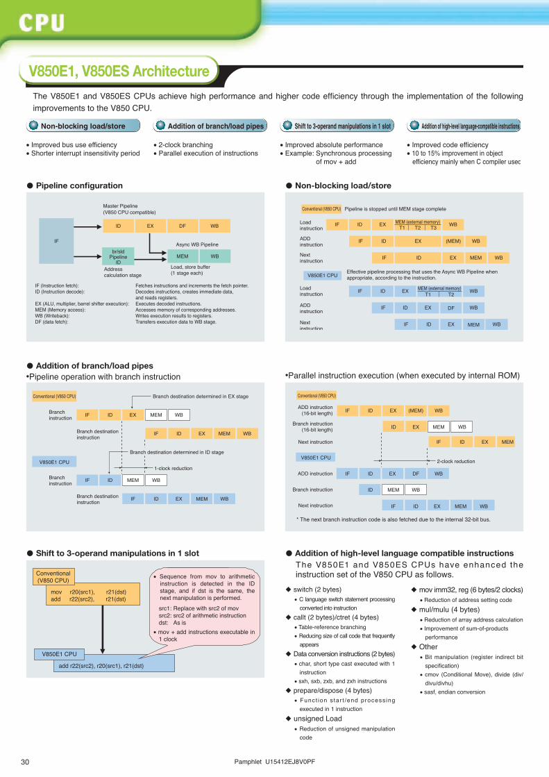
�0 Pamphlet U15412EJ8V0PF
The V850E1 and V850ES CPUs achieve high performance and higher code efficiency through the implementation of the following improvements to the V850 CPU.
l Shift to 3-operand manipulations in 1 slot
IF
WB
br/sldPipeline
IDWB
Master Pipeline(V850 CPU compatible)
Async WB Pipeline
Addresscalculation stage
Load, store buffer(1 stage each)
ID DF
MEM
EX
IF (Instruction fetch): Fetches instructions and increments the fetch pointer. ID (Instruction decode): Decodes instructions, creates immediate data,
and reads registers. EX (ALU, multiplier, barrel shifter execution): Executes decoded instructions. MEM (Memory access): Accesses memory of corresponding addresses. WB (Writeback): Writes execution results to registers. DF (data fetch): Transfers execution data to WB stage.
l Pipeline configuration
WBLoadinstruction
EX
V850E1 CPU
Nextinstruction
ADDinstruction
Loadinstruction
Nextinstruction
ADDinstruction
MEM (external memory)T1 T2 T3
Pipeline is stopped until MEM stage complete
Effective pipeline processing that uses the Async WB Pipeline whenappropriate, according to the instruction.
IF ID EX
Conventional (V850 CPU)
WBMEMIF ID
WB(MEM)EXIDIF
WB
WB
DF
MEM
EXIF ID T1 T2MEM (external memory) WB
IF EXID
IF ID EX
l Non-blocking load/store
Conventional (V850 CPU)
EX
Branchinstruction
Branchinstruction
Branch destination determined in EX stage
MEM WB
V850E1 CPU
Branch destinationinstruction
Branch destinationinstruction
MEM
IF ID
IF ID EX WBMEM
MEM WBIF ID
IF ID EX WB
Branch destination determined in ID stage
1-clock reduction
•Parallel instruction execution (when executed by internal ROM)l Addition of branch/load pipes •Pipeline operation with branch instruction
ADD instruction(16-bit length)
V850E1 CPU
Next instruction
Branch instruction(16-bit length)
ADD instruction
Next instruction
Branch instruction WBMEM
WBMEM
WBMEM
IF ID EX WB(MEM)
ID EX
Conventional (V850 CPU)
IF ID EX MEM
IF ID EX WBDF
ID
IF ID EX
2-clock reduction
Conventional(V850 CPU)
V850E1 CPU
add r22(src2), r20(src1), r21(dst)
mov r20(src1), r21(dst) add r22(src2), r21(dst)
• Sequence from mov to arithmetic instruction is detected in the ID stage, and if dst is the same, the next manipulation is performed. src1: Replace with src2 of movsrc2: src2 of arithmetic instructiondst: As is
• mov + add instructions executable in 1 clock
• Improved bus use efficiency • Shorter interrupt insensitivity period
• 2-clock branching • Parallel execution of instructions
• Improved absolute performance • Example: Synchronous processing
of mov + add
• Improved code efficiency • 10 to 15% improvement in object
efficiency mainly when C compiler used
Non-blocking load/store Addition of branch/load pipes Shift to 3-operand manipulations in 1 slot Addition of high-level language-compatible instructions
* The next branch instruction code is also fetched due to the internal 32-bit bus.
l Addition of high-level language compatible instructionsThe V850E1 and V850ES CPUs have enhanced the instruction set of the V850 CPU as follows.
V850E1, V850ES Architecture
u switch (2 bytes) • C language switch statement processing
converted into instruction u callt (2 bytes)/ctret (4 bytes)
• Table-reference branching • Reducing size of call code that frequently
appears u Data conversion instructions (2 bytes)
• char, short type cast executed with 1 instruction
• sxh, sxb, zxb, and zxh instructions u prepare/dispose (4 bytes)
• Funct ion s tar t /end process ing executed in 1 instruction
u unsigned Load • Reduction of unsigned manipulation
code
u mov imm32, reg (6 bytes/2 clocks)• Reduction of address setting code
u mul/mulu (4 bytes) • Reduction of array address calculation• Improvement of sum-of-products
performance u Other
• Bit manipulation (register indirect bit specification)
• cmov (Conditional Move), divide (div/divu/divhu)
• sasf, endian conversion

Pamphlet U15412EJ8V0PF �1
......................................
............................
......
.................
.................................................
............................................................
......
.................
............................
......................................
.................................................
............................................................
Instruction 2completion
Instruction 4completion
Instruction 1Instruction 6completion
Instruction 3Instruction 8completion
Instruction 5Instruction 10completion
Instruction 7Instruction 12completion
Instruction 9completion
Instruction 11completion
Instructions executed in each clock
Instruction 1
Instruction 2
Instruction 3
Instruction 4
Instruction 5
Instruction 6
Instruction 7
Instruction 8
Instruction 9
Instruction 10
Instruction 11
Instruction 12
Time flow
Internal system clockProcessing simultaneously
performed by CPU
<1> <2> <3> <4> <5> <6> <7> <8> <9> <10> <11> <12>
IF DPID
EX WB
EX AT WBDF
ID
IF DPID
EX WB
EX AT WBDF
ID
IF DPID
EX WB
EX AT WBDF
ID
IF DPID
EX WB
EX AT WBDF
ID
IF DPID
EX WB
EX AT WBDF
ID
IF DPID
EX WB
EX AT WBDF
ID
V850E2 CPU features V850E2 CPU Main added functions
Execution of up to 2 instructions/clock possible (dependent on instruction sequence)
V850E2 CPU pipeline operation
Reg
iste
r file
Instruction memory, instruction cache
Instru
ction
exec
ution
pipeli
ne le
ft (L-
pipe)
BSFTunit
ALUunit
ALUunit
MEMunit
MULunit
Data memory, data cache
Inst
ruct
ion
fetc
h pi
pelin
e (F
-pip
e)
Inst
ruct
ion
fetc
h un
it (B
-pip
e)
Inst
ruct
ion
buffe
r
Dis
patc
h un
it
Instru
ction
exec
ution
pipeli
ne rig
ht (R
-pipe
)
Inst
ruct
ion
deco
de u
nit R
Inst
ruct
ion
deco
de u
nit L
Writ
e ba
ck u
nit
2 instructions simultaneously executable using 2 instruction execution units
V850E2 CPU pipeline configuration
V850E2 Architecture
Real-time performance of 250 MIPS - Operation at over 200 MHz Inheritance of V850E1 performance and features - Upward instruction compatibility with V850E1 and
V850ES CPUs at object level - Use of 7-stage pipeline - Parallel pipeline configuration (2 parallel superscalar) - 128-bit instruction fetch bus Support of expanding application software sizes - Address space (program/data) expansion - Strengthened cache memory support
32-bit relative branch instruction - Support of program space expansion - Long-distance branching performance, elimination of code efficiency losses 3-operand instructions (addition of target operations) - Higher speed processing of operations such as multiplex
add/subtract (64-bit operation, saturate operation) and bit shift, contributing to higher code efficiency
Sum-of-products instruction- Higher speed 32-bit sum-of-products operation (32 × 32 + 64 ‡ 64 bits) Bit search instruction- Bit row change point search for run length measurement,
contributing to increased speed of conversion from integers to floating decimals, etc.
IF: Instruction fetchDP: DispatchID: Instruction decodeEX: Instruction executionAT: Address transferDF: Data fetchWB: Writing execution result to register
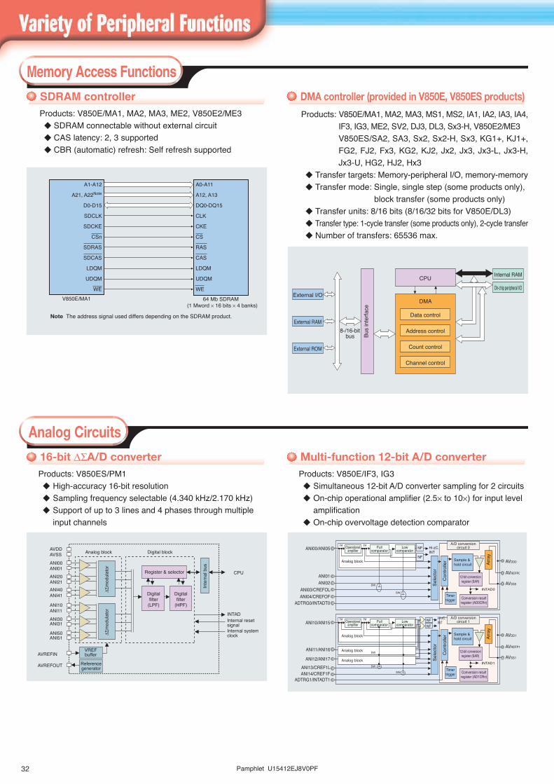
�� Pamphlet U15412EJ8V0PF
Products: V850E/MA1, MA2, MA3, ME2, V850E2/ME3 u SDRAM connectable without external circuitu CAS latency: 2, 3 supportedu CBR (automatic) refresh: Self refresh supported
Products: V850E/MA1, MA2, MA3, MS1, MS2, IA1, IA2, IA3, IA4, IF3, IG3, ME2, SV2, DJ3, DL3, Sx3-H, V850E2/ME3V850ES/SA2, SA3, Sx2, Sx2-H, Sx3, KG1+, KJ1+, FG2, FJ2, Fx3, KG2, KJ2, Jx2, Jx3, Jx3-L, Jx3-H, Jx3-U, HG2, HJ2, Hx3
u Transfer targets: Memory-peripheral I/O, memory-memoryu Transfer mode: Single, single step (some products only),
block transfer (some products only)u Transfer units: 8/16 bits (8/16/32 bits for V850E/DL3)u Transfer type: 1-cycle transfer (some products only), 2-cycle transferu Number of transfers: 65536 max.
A0-A11
A12, A13
DQ0-DQ15
CLK
CKE
CS
RAS
CAS
LDQM
UDQM
WE
64 Mb SDRAM (1 Mword × 16 bits × 4 banks)
A1-A12
A21, A22Note
D0-D15
SDCLK
SDCKE
CSn
SDRAS
SDCAS
LDQM
UDQM
WEV850E/MA1
Note The address signal used differs depending on the SDRAM product.
CPU
DMA
Data control
Address control
Count control
Channel controlBu
s in
terfa
ce
External I/O
External RAM
Internal RAM
On-chip peripheral I/O
External ROM
8-/16-bitbus
SDRAM controller DMA controller (provided in V850E, V850ES products)
Memory Access Functions
Multi-function 12-bit A/D converterProducts: V850E/IF3, IG3u Simultaneous 12-bit A/D converter sampling for 2 circuitsu On-chip operational amplifier (2.5× to 10×) for input level
amplificationu On-chip overvoltage detection comparator
ANI00/ANI05 Operationalamplifier
Operationalamplifier
Analog block
Analog block
Analog block
Analog block
A/D conversioncircuit 0
A/D conversioncircuit 1
Sample &hold circuit
Conversion resultregister (AD0CRn)
NF
NF
NFNF
Hi-zC,INT
Hi-zC,INT
SW SW
Fullcomparator
Fullcomparator
Lowcomparator
Lowcomparator
SW SW
ANI01ANI02
ANI03/CREFOLANI04/CREFOF
ADTRG0/INTADT0
Sele
ctor
Sele
ctor
Arra
yAr
ray
ANI10/ANI15
ANI11/ANI16
ANI12/ANI17
ANI13/CREF1LANI14/CREF1F
ADTRG1/INTADT1
AVDD0
AVREFP0
AVSS0
AVDD1
AVREFP1
AVSS1
INTAD0
Sample &hold circuit
12-bit conversionregister (SAR)
12-bit conversionregister (SAR)
Conversion resultregister (AD1CRn)
Timertrigger
Timertrigger
Con
trolle
rC
ontro
ller
INTAD1
SW
SW
SW
SW
SW
16-bit ∆ΣA/D converterProducts: V850ES/PM1u High-accuracy 16-bit resolutionu Sampling frequency selectable (4.340 kHz/2.170 kHz)u Support of up to 3 lines and 4 phases through multiple
input channels
ANI00ANI01
Referencegenerator
Internal systemclock
AVREFINVREFbuffer
ANI20ANI21ANI40ANI41
ANI10ANI11
ANI30ANI31
ANI50ANI51
CPU
Analog block Digital block
INTADInternal resetsignal
AVDDAVSS
Inte
rnal
bus
Digitalfilter
(LPF)
Digitalfilter
(HPF)
Register & selector
∆Σm
odul
ator
∆Σm
odul
ator
AVREFOUT
Analog Circuits

Pamphlet U15412EJ8V0PF ��
Multi-function 10-bit A/D converter
Products: V850E/IA3, IA4V850ES/IK1, IE2
u Simultaneous 10-bit A/D converter sampling for 2 circuitsu On-chip operational amplifier (2.5×/5×) for input level
amplification (IA3, IA4 only)u On-chip overvoltage detection comparator (IA3, IA4 only)
+−
+
−
+−
ANI05Through modeOperational amplifier
Low
Full
Comparator
Amplification mode
ANI15ANI16ANI17
12-bit A/D
CREFnL
CREFnF
Edgedetection
Programmablenoise filter
INT
Hi-Z
Edgedetection
Programmablenoise filter INT
Hi-Z
Operational amplifier, comparatorProducts: V850E/IF3, IG3u Input voltage settable in range of 2.5 times to 10 timesu Overcurrent detectable at positive and negative sidesu Timer output pin settable to high impedance after
detection of overcurrent
Products: V850E/MA1, MA3, ME2, IA1, IA2, MS1, SV2,V850ES/Jx2, Hx2, etc.
u Conversion startable by software or hardwareu Select/scan mode switching possible
10-bit A/D converter (multi-stage buffer type)
ANI0
ANIn
ADTRG
AVREF
AVSS
INTAD
Successive approximationregister
Conversion control circuit
Conversion result register 0Conversion result register 1Conversion result register 2
Conversion result register 3Conversion result register 4
Conversion result register 5Conversion result register 6Conversion result register 7
Sele
ctor
Tap
sele
ctor
Products: V850ES/KG1+, KJ1+, SA2, SA3, Sx2, Sx2-H, Sx3, KG2, KJ2, Jx2, Jx3, Jx3-L, Jx3-H, Jx3-U, V850E/MA3, Sx3-H, V853
u R-2R ladder method (excluding V850ES/SA2, SA3)u R string method (V850ES/SA2, SA3 only)u 8-bit resolutionu Operation mode: Normal mode/real-time output mode
D/A converter
ANO0
AVREF1
AVSS
Conversion valuesetting register 0
Conversion valuesetting register 1
R-2R ladder orR string
R-2R ladder orR string ANO1

�� Pamphlet U15412EJ8V0PF
Products: V850E/IA1, IA2, IA3, IA4, MA3, ME2,V850E2/ME3
u 16-bit 2-phase encoder input possibleu Compare registers: 2
Capture/compare registers: 2
Up/down counter
TCLR
TIUD
TCUD
Capture/compareregister
Selector 16-bit up/down counter timer
Compareregister
Compareregister
CLRcircuit
INTCC0
INTCC1
INTCM0
INTCM1
TO
Edgedetection
circuitOutputcontrol
Capture/compareregister
Timer/Counter
Products: V850ES/SA2, SA3, PM1, Jx3-H, Jx3-U, V850E/Sx3-Hu On-chip week, day, hour, minute, second countersu Counting up to 4095 periodsu Support of interval interrupt generation at fixed intervals
selectable from: 0.015625 s, 0.03125 s, 0.0625 s, 0.125 s, 0.25 s, 0.5 s, 1 s, 1 mn, 1 hr, 1 day
Real-time counter
INTROVPrescaler
3
Subcountregister(15 bits)
INTRTC
Weekcount
register(12 bits)
1 s
0.015625 s/0.03125 s/0.0625 s/0.125 s/0.25 s/0.5 s
Count clock= 32.768 kHz
6
1 mn 1 hr 1 day
Sele
ctor
Sele
ctor
fXT
fBRG
Count enable/disable circuit
Internal bus
Minutecount
register(6 bits)
Hourcount
register(5 bits)
Day countregister(3 bits)
Secondcount
register(6 bits)
Second countspecification
register
Minute countspecification
register
Hour countspecification
register
Day countspecification
register
Week countspecification
register
Products: V850E/SV2u 32-bit timer unit for servo controlu Capture registers: 12
Compare registers: 2u External input detection circuit with 1 to 256 dividersu On-chip 8-bit mask timers: 2
32-bit servo timer
Sele
ctor
Clear & countcontrol
TM3 (32-bit)
CP3x (32-bit)
CP3y (32-bit)
CP3z (32-bit)
CM30 (32-bit)
CM31 (32-bit)
INTOV3
INTTI3
ICP3x INTCP3xCapture
Clear
CPTTRGx
INTCP3yCapture
INTCP3zCapture
INTCM30Match
INTCM31Match
Masktimer
EDVCMx
EDVCMy
TRGx
SLCLK
TI3 TI3
DividerNoise elimination Edge detection
Noise elimination Edge detection
2ch (x=0-1)
ICP3y TRGy DividerNoise elimination Edge detection
2ch (y=2-3)
ICP3z TRGzNoise elimination Edge detection
8ch (z=4-11)
{fxx-fxx/8 (4)
fxx
A/D trigger
Outputcontrol
TMQOP
16-bit capture/compareInterrupt signal
Interrupt signalClear
INTOVF
control
Interrupt signal
Interrupt signal
16-bit capture/compare
16-bit capture/compare
TMQ
TMP
16-bit capture/compare
Timer Output
A/D capture timing generation
Output duty generation
Sync start supported
TM outputcontrol
6-phasePWMoutputcontroller
A/D operationtrigger control
16-bit counter
U
U
V
V
W
W
Timer Output
Timer Output
Output period generation
Timer configuration during inverter control
Products: V850E/IA3, IA4, IF3, IG3, MA3, V850ES/IK1, IE2, Fx3, Hx3
u 0% and 100% output and 6-phase PWM output with deadtime possible
u Switchable anytime/batch overwrite for compare registeru A/D converter conversion start trigger generator

Pamphlet U15412EJ8V0PF ��
Products: V850E/SV2, V850ES/KF1+, KG1+, KJ1+, KF2, KG2, KJ2
u 32-byte internal buffer RAMu Automatic send/receive function
• 1 to 32 bytes of transfer bytes specifiable• Transfer interval specifiable (0 to 63 clocks)• Single transfer/repeated transfer specifiable
Products: V850ES/Kx1+, Sx2, Sx2-H, Sx3, Jx2, Jx3, Jx3-L, Jx3-H, Jx3-U, Hx2, Hx3, V850ES/Fx2, Fx3, Fx3-L, V850E/Dx3
u Low-cost 1-line network busu Sync break field (SBF) send/receive possible through
hardware(Send: 13 bits ≤ SBF ≤ 20 bits; Receive: SBF ≥ 11 bits)
u Also generally usable as UART
SIAn
DIRn
Internal bus
SOAn
INTCSIAn
fxx/6-fxx/256
MASTERn
Automatic data transferaddress count register
Automatic data transfer addresspoint specification register
Serial clockcounter
Interruptgenerator
Selector
Buffer RAM(32 bytes)
Serial I/Oshift register
SCKAnSerial transfercontrol circuit
6-bit counter
Automatic datatransfer interval
specification register
Port configuration for LIN reception
LIN reception pin
External interrupt pin
Timer input pin
Timer
SBF automatic detection
Receptioncircuit
Edge detectioninterrupt
Flag
Selector Wakeup detection
Capture input
Flag
SelectorBaud rate error detection through capture timer
Timer output selectable as source clock‡Any baud rate selectable
LIN transmission circuit
LINtransmission pin
Timer output selectable as source clock‡Any baud rate selectable!!
SBF automatic transmission
Selector
Flag
Timer
Transmissioncircuit
Able to invert output
Internally connectable by software,so external connection not required!
LINBusSerial interface with automatic send/receive function
Serial Interface
InterruptrequestCRXD
CTXD MAC(Message
AccessController)
Controlcircuit
CAN module
CAN RAM(message buffer)
CAN protocoltransfer block
Products: V850ES/Sx2, Sx2-H, Sx3, Fx2, Fx3, Fx3-L, Jx3-H, V850E/IA1, Dx3, Sx3-H, V850/SC3
u CAN protocol ver. 2.0 Part B (send/receive of standard and extended frames)
u Max. transfer rate: 1 Mbpsu 32 message buffer
CAN
Products: V850ES/SG1, Sx2, Sx2-H, Sx3, V850E/Sx3-H,V850/SB2, SC2
u Communication mode 1 supportedu Max. transfer bytes: 32 bytes/frameu Max. transfer speed: Approx. 26 kbps
IETX
IERX
Interruptrequest
Register block
Control block
Bitcontroller
Fieldcontroller
Transmissionblock
Receptionblock
IEBus controller

�� Pamphlet U15412EJ8V0PF
Products: V850E/ME2V850E2/ME3
u Compliant with Universal Serial Bus Specificationu Support of 12 Mbps (full speed) transferu Many endpoint configurations
Products: V850/SB1, SB2, SC1, SC2, SC3V850ES/SA2, SA3, SG1, Sx2, Sx2-H, Sx3, KE1+, KF1+, KG1+, PM1, IK1,V850E/MA3, SV2, IA3, IA4, Dx3, Sx3-H
u Instructions of address to be modified inserted to replace DBTRAP instruction (JMP r0 instruction in case of V850 CPU), branching to 0060H (0000H in case of V850 CPU)
u Program modification following switch to mask ROM possibleu Modified addresses: 4 points, 8 pointsNote
Note V850E/SV2, DJ3, Sx3-H
Note JMP r0 instruction in case of V850 CPU
USB function 0 DMAchannel select
register (UF0CS)
USB function 0 buffercontrol register (UF0BC)
UFDRQnDMAAKn
TCn
USBSP2BUSBSP4B
INTUSB0BINTUSB1BINTUSB2BINTRSUM
fUSB (48 MHz)
Remark n = 0 to 3
Sele
ctor
UDM
UDP
USB
I/O Buffer
Control transfer: Endpoint0R (64 bytes)/Endpoint0W (64 bytes) Bulk transfer 1: Endpoint1 (64 bytes × 2)/Endpoint2 (64 bytes × 2) Bulk transfer 2: Endpoint3 (64 bytes × 2)/Endpoint4 (64 bytes × 2) Interrupt transfer1/2: Endpoint7 (8 bytes)/Endpoint8 (8 bytes)
Endpoint
SIE
RSUM_OUT
USB SSCG function (Spread spectrum Frequency Synthesizer Clock Generator)
ROM correction function Explanation of ROM correction operation
Downloadmodificationprogram
Correctionaddress enablesetting information
ROM correctionrequest flag = 0?
Yes
No
Read modificationprogram to RAM
Correction addresssettingROM correction enable
Replace DBTRAPinstructionNote
Main routine
Normal flow
ROM correction flow
Internal ROM
External ROM,EEPROM, etc.
Internal RAM
Return tointernal ROM
Modificationprogram execution
RESET
Jump tomodification program
ROM correctionrequest flag clear
Correction address = XXXXROM correctionenable flag = 1
Next processing...
Correction point
Initialization
Modificationprogram download
Comparator
Output triggercontrol circuit
DBTRAP instructionNote
generation block
Internal ROM
Instructionreplacement part
Instruction data bus
ROM correctionaddress register
Instruction address bus
Products: V850E/ME2, Dx3, Sx3-H, V850ES/Hx3, Fx3V850E2/ME3
u EMI peak noise reduction through input frequency modulation
u Large reduction in noise countermeasure time and cost possible
u Frequency modulation rate and modulation period changeable by register setting
Modulation periodWithout frequency modulation With frequency modulation rate of -3%‡Modulation period: 13 to 27 kHz
Improvement of10 dB or more
Freq
uenc
ym
odul
atio
n ra
te
Note JMP r0 instruction for the V850 CPU
Other

Pamphlet U15412EJ8V0PF ��
V850 Flash
Target system
On-chip debug emulatorMINICUBE
Host machine
• Break function • Execute function• Pin mask function• Download function• Execution time measurement• Non-use of user resources
Clock monitor function
On-chip debugging function Boundary scan function
Main clockInternal reset signal
Internal oscillationclock
reset
enable
Flag
Reset upon abnormal stop Main clock oscillation monitoring
Run/stop settable by software
+
---
Referencevoltage
Flag
Interrupt signal
VDD
VDD
Reset signal
Sele
ctor
Det
ectio
n le
vel s
elec
tion
Resis
torRe
sistor
Resis
tor
Products: V850ES/Kx1+, Sx2, Sx3, Fx2, Fx3, Fx3-L, Jx2,Jx3, Jx3-L, Jx3-H, Jx3-U, Hx2, Hx3, IK1, IE2V850E/IF3, IG3, Sx3-H
u Detection voltage level changeable by softwareu Usable instead of reset IC, contributing to lower system costu Detection voltage not changeable after mode transition
(security protection)
Products: V850E/IA3, IA4, IF3, IG3, Dx3, Sx3-H, V850ES/Kx1+, SG1, Sx2, Sx2-H, Sx3, Fx2, Fx3, Fx3-L, Jx2, Jx3, Jx3-L, Jx3-H, Jx3-U, Hx2, Hx3, IK1, IE2
u Monitors abnormal stops of main clock with internal oscillatoru During abnormal stop, entire system can be set to reset statusu Prevention of destruction due to system deadlock or program loop
Products: V850E/ME2Note 1, V850E2/ME3Note 2, V850E/MA3, IA4, IG3, SV2, V850E/DJ3, DL3, Sx3-H, V850ES/KJ1+, KJ2, Sx2, Sx2-H, Sx3, Fx2, Fx3, Fx3-L, Jx2, Jx3, Jx3-L, Jx3-H, Jx3-U, Hx2, Hx3
u Realization of on-chip debugging of microcontroller with DCU(Debug Control Unit)
u Compact and low-cost on-chip emulatoru Download functionu Integrated debugger (ID850QB) supported
Notes 1. Trace function support is possible by using the RTE-2000-TP made by Midas Lab Co., Ltd., or PARTNER-ET II, PARTNER-J made by Kyoto Micro Computer Co., Ltd.
2. Trace function support is possible by using the RTE-2000-TP made by Midas Lab Co., Ltd.
Products: V850E/SV2u Use of JTAG (Joint Test Action Group) communication
specifications, IEEE1149.1 compliantu Progressive scan of device’s external I/O pins, test data
input/output possibleu Connection check of devices soldered on user board possible
TCK
TDI
I/O
I/O
I/O
I/O
TMSTRST
TDO
Bypass register
Instruction register
Decoder
Internal logic
Sele
ctor
Sele
ctor
TPA controller
Boundary scan register
: Boundary scan target pin : JTAG interface pin : Boundary scan cell
Low-voltage detector (LVI)
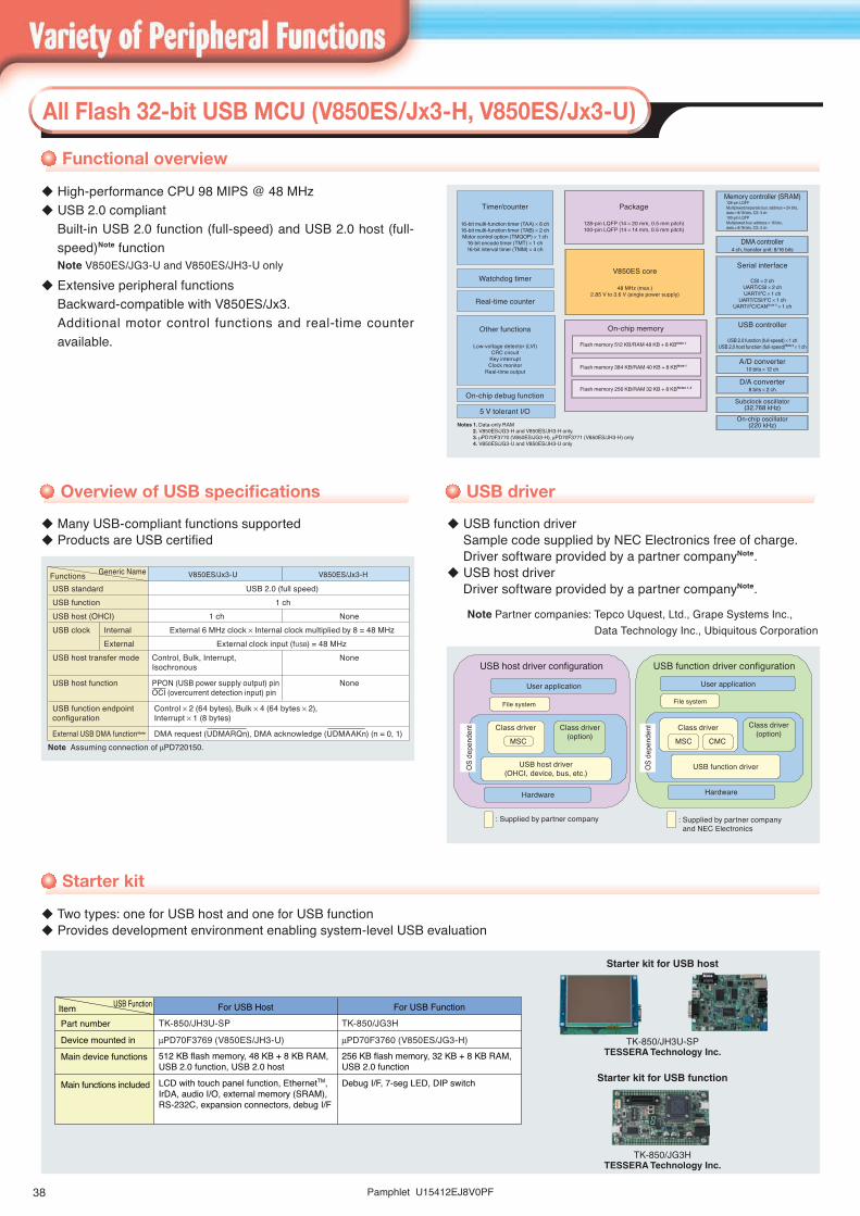
�� Pamphlet U15412EJ8V0PF
u High-performance CPU 98 MIPS @ 48 MHzu USB 2.0 compliant
Built-in USB 2.0 function (full-speed) and USB 2.0 host (full-speed)Note functionNote V850ES/JG3-U and V850ES/JH3-U only
u Extensive peripheral functionsBackward-compatible with V850ES/Jx3.Additional motor control functions and real-time counter available.
u Many USB-compliant functions supportedu Products are USB certified
Functional overview
Overview of USB specifications USB driver
NonePPON (USB power supply output) pinOCI (overcurrent detection input) pin
USB host function
External clock input (fUSB) = 48 MHzExternalInternal
USB 2.0 (full speed)USB standard
External 6 MHz clock × Internal clock multiplied by 8 = 48 MHzUSB clock
1 chUSB function
NoneControl, Bulk, Interrupt,Isochronous
USB host transfer mode
None
V850ES/Jx3-H
DMA request (UDMARQn), DMA acknowledge (UDMAAKn) (n = 0, 1)External USB DMA functionNote
Control × 2 (64 bytes), Bulk × 4 (64 bytes × 2),Interrupt × 1 (8 bytes)
1 ch
V850ES/Jx3-U
USB function endpointconfiguration
USB host (OHCI)
Note Assuming connection of µPD720150.
Functions Generic Name
All Flash 32-bit USB MCU (V850ES/Jx3-H, V850ES/Jx3-U)
Package
128-pin LQFP (14 × 20 mm, 0.5 mm pitch)100-pin LQFP (14 × 14 mm, 0.5 mm pitch)
V850ES core
48 MHz (max.)2.85 V to 3.6 V (single power supply)
On-chip memory
Flash memory 512 KB/RAM 48 KB + 8 KBNote 1
Flash memory 384 KB/RAM 40 KB + 8 KBNote 1
Flash memory 256 KB/RAM 32 KB + 8 KBNotes 1, 2
Timer/counter
16-bit multi-function timer (TAA) × 6 ch16-bit multi-function timer (TAB) × 2 chMotor control option (TMQOP) × 1 ch
16-bit encode timer (TMT) × 1 ch16-bit interval timer (TMM) × 4 ch
Other functions
Low-voltage detector (LVI)CRC circuit
Key interruptClock monitor
Real-time output
5 V tolerant I/O
On-chip debug function
Watchdog timer
Real-time counter
A/D converter10 bits × 12 ch
Serial interface
CSI × 2 chUART/CSI × 2 chUART/I2C × 1 ch
UART/CSI/I2C × 1 chUART/I2C/CANNote 3 × 1 ch
D/A converter8 bits × 2 ch
Memory controller (SRAM)128-pin LQFPMultiplexed/separate bus: address = 24 bits,data = 8/16 bits, CS: 3 ch100-pin LQFPMultiplexed bus: address = 16 bits,data = 8/16 bits, CS: 3 ch
DMA controller4 ch, transfer unit: 8/16 bits
On-chip oscillator(220 kHz)
Subclock oscillator(32.768 kHz)
USB controller
USB 2.0 function (full-speed) × 1 chUSB 2.0 host function (full-speed)Note 4 × 1 ch
Notes 1. Data-only RAM2. V850ES/JG3-H and V850ES/JH3-H only.3. µPD70F3770 (V850ES/JG3-H), µPD70F3771 (V850ES/JH3-H) only4. V850ES/JG3-U and V850ES/JH3-U only
u USB function driverSample code supplied by NEC Electronics free of charge.Driver software provided by a partner companyNote.
u USB host driverDriver software provided by a partner companyNote.
Note Partner companies: Tepco Uquest, Ltd., Grape Systems Inc.,Data Technology Inc., Ubiquitous Corporation
User application
Hardware
File system
OS
depe
nden
t
USB host driver configuration
USB host driver(OHCI, device, bus, etc.)
Class driver
: Supplied by partner company
USB function driver configuration
USB function driver
: Supplied by partner companyand NEC Electronics
OS
depe
nden
t
User application
File system
Class driver
MSC CMC
Hardware
MSC
Class driver(option)
Class driver(option)
u Two types: one for USB host and one for USB functionu Provides development environment enabling system-level USB evaluation
Starter kit
Debug I/F, 7-seg LED, DIP switchLCD with touch panel function, EthernetTM,IrDA, audio I/O, external memory (SRAM),RS-232C, expansion connectors, debug I/F
Main functions included
TK-850/JG3HTK-850/JH3U-SPPart number
256 KB flash memory, 32 KB + 8 KB RAM,USB 2.0 function
512 KB flash memory, 48 KB + 8 KB RAM,USB 2.0 function, USB 2.0 host
Main device functions
µPD70F3760 (V850ES/JG3-H)
For USB Function
µPD70F3769 (V850ES/JH3-U)
For USB Host
Device mounted in
Item USB Function
Starter kit for USB host
Starter kit for USB function
TK-850/JH3U-SPTESSERA Technology Inc.
TK-850/JG3HTESSERA Technology Inc.

Pamphlet U15412EJ8V0PF ��
MEMO

�0 Pamphlet U15412EJ8V0PF
V850ES-20 MHz
A 16-bit 20 MHz
A 16-bit 16 MHz
B 32-bit 50 MHz
V850ES-20 MHz
A 16-bit 20 MHz
A 16-bit 16 MHz
B 32-bit 50 MHz
10 2 3 4 5
0 0.2 0.4 0.6 0.8 1.0 1.2 1.4 1.6
4.1
1.7
1.0
3.6
0.97
1.00
1.37
1.18
n Arithmetic processing performance comparison
n Code size comparison
(Relative comparison)
(Relative comparison)
* NEC Electronics measurement results using sample program
Cycle time 0.2 ms 0.4 ms
78K0S
78K0
78K0/Kx1
V850ES-20 MHz
0.24
0.20
0.05
0.40
78K4 0.125
32-bit RISC
16-bit CISC
8-bit CISC
: 12 MHz (0.168 ms) supported for some products : 10 MHz (0.2 ms) supported for some products
Minimum instruction execution time V850 arithmetic processing performance and code size
Clock gear function Standby mode
Operatingcurrent
fxx/8(2.5 MHz)
fxx(20 MHz)
fxx/32(625 kHz)
fXT(32.768 kHz)
Operatingfrequency
Reduction to 1/400by switching from main
clock to subclock
Reduction to 1/10ththrough clock gear (1/32)
Reduction to 1/5ththrough clock gear (1/8)
CPUSub
Oscillation circuit
or
or
Operating current
Normaloperation mode
HALT mode
IDLE mode
Sub normaloperation mode
Sub IDLE mode
STOP mode(sub operation)
STOP mode(sub stop)
Approx. 1/2
Approx. 1/10
Approx. 1/400
Approx. 1/4000
Approx. 1/4000
Approx. 1/15000
Operating Stopped
Peripheralfunction
Watchtimer Main
V850 Benchmark
The V850 microcontrollers realize high speed, high performance, and high code efficiency.
Low Power ConsumptionThanks to a thorough energy-saving design, the V850ES/Jx3-L attains a current/performance ratio of 0.28 mA/MIPS. As a result, compared with the 32-/16-bit microcontrollers made by other manufacturers and having equivalent performances, power consumption is reduced over 65%. Lower system power consumption and higher system performance are simultaneously achieved through the V850's extremely high power performance.
Power performance
mA/MIPS
2.5
Operating current/performance
3.0
Reduction of 27.5%
V850ES/Jx3-L
V850ES/Jx3
16-bit microcontrollersof competitors
32-bit microcontrollersof competitors
0.58
0.28
0.80
0.82
Reduction of 65%
16-bit microcontrollersof competitors
32-bit microcontrollersof competitors

Pamphlet U15412EJ8V0PF �1
n In case of V850ES/JJ2 (Flash memory: 640 KB)
Supply voltage 3.3 V
Operating frequency 20 MHz
EMS countermeasures EMS measurement results (power supply coupling measurement)
EMS noise measurement results
Voltage controloscillator
To CPUperipheralfunctions
Oscillationcircuit
Phase comparator LPF VCO
Divider
nUse of PLL for oscillation circuit
High-frequency noise cutthrough PLL filter
Minimizing the influence of electromagnetic interference (EMI) emitted from the microcontroller and the influence of noise applied to the microcontroller (EMS) is a high priority, particularly for AV equipment such as car infotainment systems, and thus superior noise performance is required of microcontrollers.Various noise countermeasures are implemented in the V850 microcontrollers, and noise performance equivalent or superior to that of 16-bit products has been realized.
Noise Countermeasures
CPU power supply separationInsertion of capacitancebetween VDD and GND
Vport
Vcpu
GNDport
GNDcpu
I/OPORT
Reg. (OFF setting possible)
CPU OSCAMP
Port powersupply separation
Due to the relation between the power supply and GND pad positions and the lead frame, placement is done so as to lower the power supply impedance.
EMI noise countermeasures: Power supply circuit countermeasures
1201101009080700
10
20
30
40
50
60
Frequency [MHz]
EMI N
oise
[dBu
A]
2.0 kV or higher1.0 kV0 kV
V850ES/KJ2
Existing V850 products (PLL-less products)
Existing V850 products V850ES/KJ2 (flash version)
VDD = 5 V
Resonator: 4 MHz
Internal operation frequency: 16 MHz(PLL = ON)
VDD = 5 V
Resonator: 16 MHz
Internal operation frequency: 16 MHz
nNoise applicationvoltage

�� Pamphlet U15412EJ8V0PF
NEC Electronics supports your product development by supplying various solutions, such as ASSPs intended for particular systems, middlewareNote for complicated processing, and peripheral devicesNote for special functions. These solutions can substantially shorten the development period and reduce costs.Note Through close cooperation with our partner companies, NEC Electronics offers many solutions consisting of not only our own products but also of products from partner company.
Controlling a motor can be easily started by using an ASSP of the V850 for inverter control application. A brushless DC (BLDC) motor is also supplied. So this evaluation kit is recommended for those who wish to "try" or "rotate" a motor.
Evaluation kit supporting "rotating" (low-voltage version motor starter kitNote)
Low-voltage version motor starter kitNote
By NEC Electronics
Note For details and purchasing, consult your NEC Electronics sales representative or distributor.
Processing performance (at 20 MHz)Note
ROM RAM Compression ExpansionSize of software
3 KB 32 bytes 15 µs max. 12 µs max. CEB-V850ES/JG2 Sound Kit(with V850ES/JG2)
By Cosmo
Sound evaluation kitsupporting "Speaking"
RUN
Temperaturesetting
Current temperatureSet temperature
Water quantity
Applicationexample
Water heater
ADPCM library(about 3 KB)
+Sound data
(about 4 KB/second)
InternalFlash
InternalRAM
D/Aconverter(or PWM) Amplifier
Speaker
The bathis ready.
Call-ingHeat-ingVolu
me
Note Processing is necessary every 125 µs in the case of 8 kHz sampling sound.
˚cc̊
System control and sound function to compress and expand sounds via software can be achieved with a single chip.
Solutions for V850
Rotating
Speaking
"Connecting" easily
Efficiently "rotating" motors
"Speaking" clearly
"Showing" clearly
• Control of systemReal-time controlDelicate control
• User interfaceInput through keyboardNotification by displayNotification by sound
• NetworkCommunication in systemCommunication between setsCommunication with external source
l Features• Speed display: 7SEGLED 4• User interface: Push-button switch 4 Variable resistor 1• PC interface: RS-232C 1• Safety: Isolation by photocoupler Overcurrent detection signal• Control signal: U-/V-/W-phase voltage U-/V-/W-phase current BEMF signal by comparator
• Parameter display by GUI• System power supply: 15 V
l Target devicesV850ES/IE2, V850ES/IK1, V850E/IG3
l Sample programs (to be released gradually)Sample programs for 120-degree excitation mode BLDC motors (Hall sensor/sensor-less) and 180-degree excitation mode BLDC motors (Hall sensor) will be available.

Pamphlet U15412EJ8V0PF ��
Several "showing" solutions are available, depending on the performance of the CPU.A touch panel screen for a system which uses a V850 All Flash microcontroller to make the most of a high-performance, 20 MHz high-capacity memory is proposed below. A solution of 3D graphics using a high-performance V850E2/ME3 is also proposed.
l Cost-effective V850ES/JG2Capable of simultaneously processing system control and graphic control
Low-end "showing" solutionl Many software libraries available
Various types of essential software, such as graphic libraries and touch panel control drivers are available.
High-end "showing" solutionl 3D graphics solution by high-end V850+MascotCapsuleTM
MascotCapsule, which has enjoyed a well-deserved reputation as a 3D drawing engine for cellular phones can easily achieve 3D graphics in an embedded microcontroller.• High-end V850 and advanced MascotCapsule produce low-cost but expression-rich 3D graphics.• Main plug-in 3D creating tools are supported, so that high-quality 3D contents can be easily developed.
Many "connecting" solutions are available, depending on the application.Low-cost solutions using a low-end V850 All Flash microcontroller are recommended for applications where only a low transfer speed is required, such as remote monitoring and remote control, and solutions using high-end V850E/ME2 or V850E2/ME3 are recommended for applications where high transfer speeds are required, such as video transmission.
Internet connection can be easily achieved at low cost with two chips: the V850 All Flash microcontroller having high-performance, high-capacity memory and compact network software, and an external Ethernet controller. This is an ideal solution for remote monitoring and remote controlling.
Low-end "connecting" solution
High-end "connecting" solutionThe V850E/ME2 and V850E2/ME3 can be used for applications where high-speed transfer functions, such as a function to transfer video data, are necessary because they can communicate data at 10 Mbps or more. Take network cameras, for example. These microcontrollers not only can process the network but can also simultaneously control the cameras.
Touch panel evaluation kit supporting "showing"
Application exampleUSBI/F
V850ES/JG2
I/F fordebugging
LCDcontroller
Return Heating Thawing
MENU
EB-850/JG2+TFT(with V850ES/JG2)By TESSERA Technology Inc.
Notes 1. The µPD760110, which is pin-compatible with the V850E2/ME3 is available and is provided with a license for MascotCapsule, which is to be used with the AG3 (V850). For details, consult your NEC Electronics sales representative or distributor.2. AG301 is a graphic LSI made by Axel Company
System configuration example Software configuration
LCD display
CGROM(texture, background data)
ROM(program)
Graphics LSIAG301
SDRAM(program and data)
V850Note 1
Graphics LSI(AG301)Note 2
Application
2D drawing(background)
MascotCapsule for AG3 (V850)(3D coordinate operation and drawing command creation)
Driver
Showing
Connecting
Ethernetcontroller
Busconnection
InternalFlash
InternalRAM
Network application(such as WEB server and mail)
Network library(TCP/IP)
Ethernet driver
"Connecting" achieved by a simple configuration that does not needan external memory.
Evaluation kit supporting "connecting"
TK-850/JG2+NET(with V850ES/JG2)By TESSERA Technology Inc.
ESPT-V850(with V850E/ME2)
By Data Technology Inc.
KBCR-CB2 image processing evaluation kitBy Shikino High Tech Co., Ltd.
Applicationexample
Development kit supporting the development of network camerasSolutions that can immediately produce network cameras

�� Pamphlet U15412EJ8V0PF
Features
Rewrite Modes
Note 1. In the case of dual-power-supply flash, VPP Note 2. In the case of dual-power-supply flash, don’t connect.
Handshake-compatible CSI communication methodCSI communication method UART communication method
Dedicated flashmemory programmer
(PG-FP5, etc.)
Example: V850ES/SA2
VDD
VSS
RESETSI0SO0SCK0
VDD
GNDRESET
SOSI
SCK
FLMD1 or VSSFLMD1FLMD0FLMD0 Note 1
Note 2
Dedicated flashmemory programmer
(PG-FP5, etc.)
Example: V850ES/SA2
VDD
VSS
RESETSI0SO0SCK0PDH0
VDD
GNDRESET
SOSI
SCKHS
FLMD1 or VSSFLMD1FLMD0FLMD0 Note 1
Note 2
Dedicated flashmemory programmer
(PG-FP5, etc.)
Example: V850ES/SA2
FLMD1 or VSS
VDD
VSS
RESETRXD0TXD0
FLMD1FLMD0FLMD0
VDD
GNDRESET
TxDRxD
Note 1
Note 2
Programming using programmer (on-board/off-board)
Flash memory can be erased and rewritten using a self-programming library from a program placed in an area outside the flash memory.
Self-programming mode (single-power-supply method) Self-programming flow
All blocks completed?
YESNO
Erase processing
Flash environment initialization processing
Write processing
Internal verify processing
Flash environment end processing
Processing end
Flash information setting processing
Boot area replacement processing
Flash memory operation
• Access to flash area prohibited • STOP instruction execution
prohibited • Clock stop prohibited
256 KB
Flash memory
Library initializationprocessing
Library endprocessing
00000H
3FFFFHBlock 7 (60 KB)
Block 6 (60 KB)
Block 5 (60 KB)
Block 4 (60 KB)
Block 3 (4 KB)Block 2 (4 KB)Block 1 (4 KB)Block 0 (4 KB)
Flash memory
Normal operation mode Self-programming mode
00000H
3FFFFH
Self-programminglibrary
(erase/writeroutine execution)
Caution The number of blocks and block capacity differ depending on the products.(Example: V850ES/SA2)
To answer the need for shorter development time and maintenance after shipping, NEC Electronics offers microcontrollers with on-chip flash memory available in a large range of capacities from 64 KB to 2048 KB as part of the V850 microcontrollers. NEC Electronics’ flash memory microcontrollers offer the following features.u Flash capacity
64 to 2048 KBu Overwrite unit
Entire memory at one time, or block unitsu Rewrite method
Serial communication with dedicated flash memory programmer (on-board, off-board)Self-flash programming
u Rewrite voltageSingle-power-supply flash: Operation voltageDual-power-supply flash: Operation voltage 7.8 V/10.3 V
u Rewrite count: 100/1,000 times
To enable integrated use ranging from development to mass production and maintenance, the V850 microcontrollers support a programmer rewrite mode that uses serial communication supporting on-board programming, as well as a self-programming mode that rewrites flash memory with user programs.u On-board programming mode
This programming mode is used to rewrite the flash memory mounted on the target system using a dedicated flash memory programmer.u Off-board programming mode
This programming mode is used to rewrite flash memory using a dedicated flash memory programmer and dedicated program adapter (FA SeriesNote 1).
u Self-programming modeThis programming mode is used to rewrite flash memory by executing the user program written beforehand to the flash memory using on-board/off-board programmingNote 2.
Notes 1. The FA Series is a product of Naito Densei Machida Mfg. Co., Ltd.2. Since instruction fetch and data access cannot be performed from the internal flash memory area during self-programming, a program for rewriting
internal RAM or external memory must be transferred in advance.
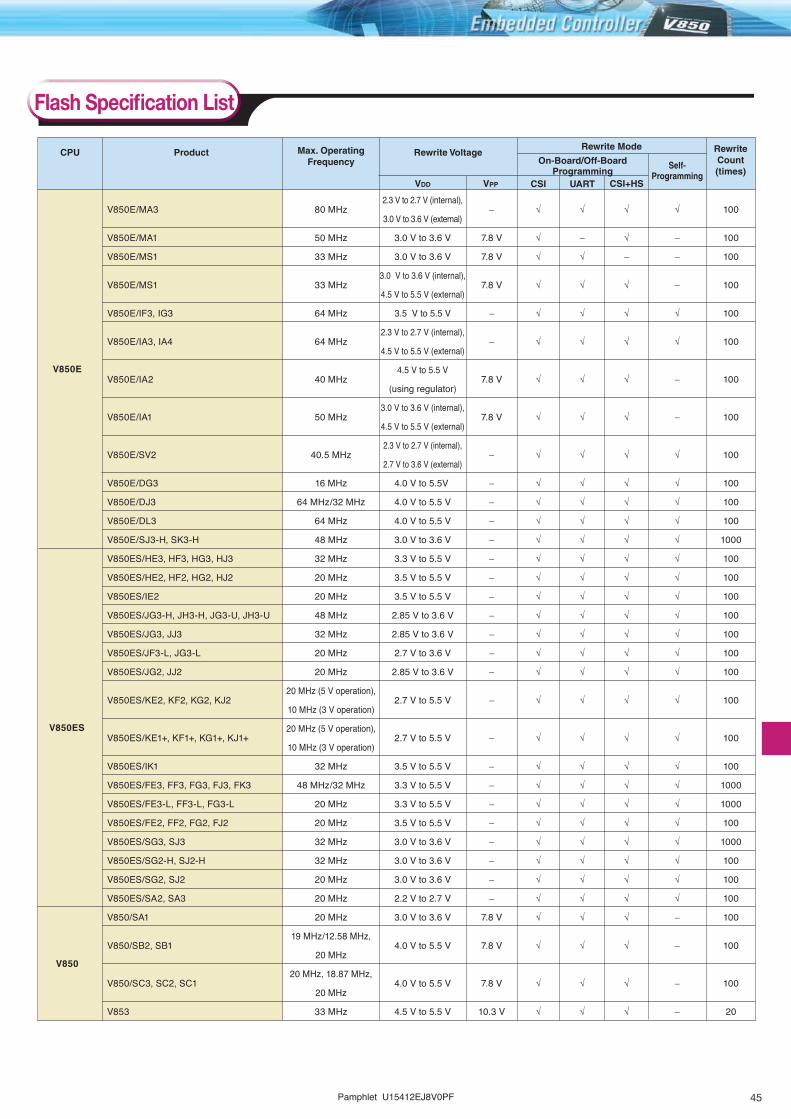
Pamphlet U15412EJ8V0PF ��
CPU
V850E
V850ES
V850
Product Rewrite VoltageRewrite Mode Rewrite
Count(times)
On-Board/Off-BoardProgramming
Self-Programming
VPP CSI UART CSI+HS
V850E/MA3
V850E/MA1
V850E/MS1
V850E/MS1
V850E/IF3, IG3
V850E/IA3, IA4
V850E/IA2
V850E/IA1
V850E/SV2
V850E/DG3
V850E/DJ3
V850E/DL3
V850E/SJ3-H, SK3-H
V850ES/HE3, HF3, HG3, HJ3
V850ES/HE2, HF2, HG2, HJ2
V850ES/IE2
V850ES/JG3-H, JH3-H, JG3-U, JH3-U
V850ES/JG3, JJ3
V850ES/JF3-L, JG3-L
V850ES/JG2, JJ2
V850ES/KE2, KF2, KG2, KJ2
V850ES/KE1+, KF1+, KG1+, KJ1+
V850ES/IK1
V850ES/FE3, FF3, FG3, FJ3, FK3
V850ES/FE3-L, FF3-L, FG3-L
V850ES/FE2, FF2, FG2, FJ2
V850ES/SG3, SJ3
V850ES/SG2-H, SJ2-H
V850ES/SG2, SJ2
V850ES/SA2, SA3
V850/SA1
V850/SB2, SB1
V850/SC3, SC2, SC1
V853
VDD
80 MHz
50 MHz
33 MHz
33 MHz
64 MHz
64 MHz
40 MHz
50 MHz
40.5 MHz
16 MHz
64 MHz/32 MHz
64 MHz
48 MHz
32 MHz
20 MHz
20 MHz
48 MHz
32 MHz
20 MHz
20 MHz
20 MHz (5 V operation),
10 MHz (3 V operation)
20 MHz (5 V operation),
10 MHz (3 V operation)
32 MHz
48 MHz/32 MHz
20 MHz
20 MHz
32 MHz
32 MHz
20 MHz
20 MHz
20 MHz
19 MHz/12.58 MHz,
20 MHz
20 MHz, 18.87 MHz,
20 MHz
33 MHz
2.3 V to 2.7 V (internal),
3.0 V to 3.6 V (external)
3.0 V to 3.6 V
3.0 V to 3.6 V
3.0 V to 3.6 V (internal),
4.5 V to 5.5 V (external)
3.5 V to 5.5 V
2.3 V to 2.7 V (internal),
4.5 V to 5.5 V (external)
4.5 V to 5.5 V
(using regulator)
3.0 V to 3.6 V (internal),
4.5 V to 5.5 V (external)
2.3 V to 2.7 V (internal),
2.7 V to 3.6 V (external)
4.0 V to 5.5V
4.0 V to 5.5 V
4.0 V to 5.5 V
3.0 V to 3.6 V
3.3 V to 5.5 V
3.5 V to 5.5 V
3.5 V to 5.5 V
2.85 V to 3.6 V
2.85 V to 3.6 V
2.7 V to 3.6 V
2.85 V to 3.6 V
2.7 V to 5.5 V
2.7 V to 5.5 V
3.5 V to 5.5 V
3.3 V to 5.5 V
3.3 V to 5.5 V
3.5 V to 5.5 V
3.0 V to 3.6 V
3.0 V to 3.6 V
3.0 V to 3.6 V
2.2 V to 2.7 V
3.0 V to 3.6 V
4.0 V to 5.5 V
4.0 V to 5.5 V
4.5 V to 5.5 V
-
7.8 V
7.8 V
7.8 V
-
-
7.8 V
7.8 V
-
-
-
-
-
-
-
-
-
-
-
-
-
-
-
-
-
-
-
-
-
-
7.8 V
7.8 V
7.8 V
10.3 V
√
√
√
√
√
√
√
√
√
√
√
√
√
√
√
√
√
√
√
√
√
√
√
√
√
√
√
√
√
√
√
√
√
√
√
-
√
√
√
√
√
√
√
√
√
√
√
√
√
√
√
√
√
√
√
√
√
√
√
√
√
√
√
√
√
√
√
√
√
√
-
√
√
√
√
√
√
√
√
√
√
√
√
√
√
√
√
√
√
√
√
√
√
√
√
√
√
√
√
√
√
√
√
-
-
-
√
√
-
-
√
√
√
√
√
√
√
√
√
√
√
√
√
√
√
√
√
√
√
√
√
√
-
-
-
-
100
100
100
100
100
100
100
100
100
100
100
100
1000
100
100
100
100
100
100
100
100
100
100
1000
1000
100
1000
100
100
100
100
100
100
20
Max. OperatingFrequency
Flash Specification List

�� Pamphlet U15412EJ8V0PF
NEC Electronics flash memory programmers
[Manufacturer/Distributor] Wave Technology Co., Ltd.
[Target DevicesNote] V850 microcontrollers
[Features]
u Realizes close to device capacity processing speed Processes verify cycles four times faster than conventional programmers
u PASS/FAIL results, checksum values, and task count displayed on computer screen in viewer-friendly color to improve operability and reduce errors
u Standardized basic algorithms and socket board enable use in a range of environments, from development to mass production
[Additional Information]
TEL: +81-3-5304-1885 FAX: +81-3-5304-1886E-mail: [email protected]: http://www.wavetechnology.co.jp/en/index.html
•Flash programming system Y3000-8
•MINICUBE2
Partner flash memory programmers (1/2)
•PG-FP5
Note Be sure to check the NEC Electronics website for the latest news and details related to target devices. Check with related manufacturers for applicability with mass-produced lines.
Flash Memory Programmers
[Features]
u Supports write to all NEC Electronics microcontrollers with internal flash memory.u Many code storing functions (Up to eight types of codes and microcontroller
information can be retained.)u Device-specific information required for writing automatically settable with
parameter filesu Supports both on-board programming and program adapter (FA Series of
Naito Densei Machida Mfg. Co., Ltd.) programming.u Small, space-saving button layout with excellent operabilityu Can be manipulated in stand-alone mode or by a dedicated application on
WindowsTM
u Automatic control from an external source is supported by a supporting command control as standard
u Supports remote interface functions that allow an external system to manipulate and check writing and OK/ERROR indication.
[Target Devices]
Support of both on-chip debugging and flash programmingV850ES/HE2, V850ES/HF2, V850ES/HG2, V850ES/HJ2, V850ES/HE3, V850ES/HF3, V850ES/HG3, V850ES/HJ3, V850ES/IE2, V850ES/JF3-L, V850ES/JG2, V850ES/JG3, V850ES/JG3-L, V850ES/JG3-H, V850ES/JG3-U, V850ES/JH3-H, V850ES/JH3-U, V850E/SJ3-HNote, V850E/SK3-HNote, V850ES/JJ2, V850ES/JJ3, V850ES/KE2, V850ES/KF2, V850ES/KG2, V850ES/KJ2, V850E/IF3, V850E/IG3,V850ES/KE1+, V850ES/KF1+, V850ES/KG1+, V850ES/KJ1+, V850ES/FE2, V850ES/FF2, V850ES/FG2, V850ES/FJ2, V850ES/FE3, V850ES/FF3, V850ES/FG3, V850ES/FJ3, V850ES/FK3, V850ES/FE3-L, V850ES/FF3-L, V850ES/FG3-L, V850ES/SG2, V850ES/SG2-H, V850ES/SJ2, V850ES/SJ2-H, V850ES/SG3, V850ES/SJ3, V850E/IA3, V850E/IA4, V850ES/IK1, V850E/MA3Note To be supported
[Features]
u Supports 8-bit to 32-bit single power supply flash memory versions.u USB support through host machine interfaceu Enables writing via a microcontroller UART and CSI-HS.u Supports both on-board programming and program adapter (FA Series of Naito Densei
Machida Mfg. Co., Ltd.) programming.u All controls are operated from host machine-dedicated GUI.u Use of host machine USB power supply eliminates the need for a power supply
adapter to be connected to the programmeru Low-cost, compact and lightu Supports on-chip debugging.
See the following website for details: http://www.necel.com/micro/en/development/asia/minicube2/minicube2.html

Pamphlet U15412EJ8V0PF ��
[Manufacturer/Distributor] Naito Densei Machida Mfg. Co.[Target Devices] V850 microcontrollers[Features]
u Supports writing to all NEC Electronics microcontrollers with internal flash memory.u Many code-storing functions (Up to eight types of codes and microcontroller information can be
retained.)u Device-specific information required for writing automatically settable with parameter filesu Supports both on-board programming and program adapter programming.u Small, space-saving button layout with excellent operabilityu Can be manipulated in stand-alone mode or by a dedicated Windows application u Automatic control from an external source is supported by supporting command control as standardu Supports remote interface functions that allow an external system to manipulate and check writing
and OK/ERROR indication.[Additional Information]
TEL: +81-42-750-4172 FAX: +81-42-750-4183E-mail: [email protected]: http://www.ndk-m.co.jp/asmis/eng/index.html
•FlashPRO V: FL-PR5
[Manufacturer/Distributor] TESSERA Technology Inc.[Target DevicesNote] V850 microcontrollers[Features]
u GANG type programmer using StickWriter as a writing moduleu Internal flash memory that can store up to eight filesu New devices can be supported by replacing the dedicated adapter boardu Stand-alone writing that does not need a computeru AC adapter supporting AC 240 V can also be used outside of Japan.[Additional Information]
TEL: +81-44-271-7533 FAX: +81-44-271-7534Website: http://www.tessera.co.jp/eng/
•NET IMPRESS series
[Manufacturer/Distributor] TESSERA Technology Inc.[Target DevicesNote] V850 microcontrollers[Features]
u Programmer for flash memory microcontrollers with single power supply enables development and mass production regardless of location.
u Compact size that can directly be connected to a USB connectoru Can be written on stand-alone basis by supplying power to the target board.u High-speed download of 1 MB hex file within about 10 secondsu Board with wirings for flash programming eliminates need for wiring processing[Additional Information]
TEL: +81-44-271-7533 FAX: +81-44-271-7534Website: http://www.tessera.co.jp/eng/
•StickWriter
Note Be sure to check the NEC Electronics website for the latest news and details related to target devices. Check with related manufacturers for applicability with mass-produced lines.
Partner flash memory programmers (2/2)
•Stick GANG Writer
[Manufacturer/Distributor] Yokogawa Digital Computer Corporation[Target DevicesNote] V850/SB1, SB2, SA1, SC3, V853, V850E/MS1, MA1, IA1, IA2, IA4, V850ES/Fx2,
Sx2, Sx3, Jx2, IE2, Hx2, Kx2, JJ3[Features]
u Enables high-speed on-board programming of on-chip/external flash memory (up to 5 Mbps)u Programming conditions for voluminous data and multiple devices (100 or more devices) can be saved,
enabling instantaneous switchingu Includes a model with a CAN interface for automotive applications (C”arNETIMPRESS)u Can be used on a stand-alone basis or remotely controlled from a computer (Windows OS)u Interface for external switch activation or PASS/ERROR signal output provided as standardu Applications provided based on proven manufacturing line performanceu Extensive customer support (domestic and international)[Additional Information]
TEL: U.S.A. +1-770-253-7000 (Yokogawa Corporation of America)Germany +49-721-9628-0 (Hitex Development Tools GmbH)France, UK +33-1-43-41-06-37 (Ashling Microsystems Ltd.)Korea +82-2-551-0660 (Yokogawa Measuring Instruments Korea Corp.)China +86-10-8522-1699 (Yokogawa Shanghai Trading Co., Ltd.)India +91-80-4158-6000 (Yokogawa India Ltd.)Other Asia +65-6241-9933 (Yokogawa Engineering Asia Pte. Ltd.)Other Countries +81-42-333-6224 (Yokogawa Digital Computer Corporation)
FAX: U.S.A. +1-770-251-6427 (Yokogawa Corporation of America)Germany +49-721-9628-149 (Hitex Development Tools GmbH)France, UK +353-61-334477 (Ashling Microsystems Ltd.)Korea +82-2-551-0665 (Yokogawa Measuring Instruments Korea Corp.)China +86-10-8522-1677 (Yokogawa Shanghai Trading Co., Ltd.)India +91-80-2852-0625 (Yokogawa India Ltd.)Other Asia +65-6241-2606 (Yokogawa Engineering Asia Pte. Ltd.)Other Countries +81-42-352-6109 (Yokogawa Digital Computer Corporation)
E-mail: [email protected]: http://www.yokogawa-digital.com/en/

�� Pamphlet U15412EJ8V0PF
Low-End Lineup (5 V Operation) (1/6)Generic Name V850ES/HE3 V850ES/HF3Part No. mPD70F3747 mPD70F3750
CPU name V850ES V850ES
CPU performance (Dhrystone) 69 MIPS (@ 32 MHz) 69 MIPS (@ 32 MHz)
Internal ROM 128 KB (flash) 256 KB (flash)
Internal RAM 8 KB 16 KB
External businterface
Bus type - -
Address bus - -
Data bus - -
Chip select signal - -
Memory controller - -
Interrupt sources Internal 43 (including one NMI) 43 (including one NMI)
External 9 (9)Note (including one NMI) 9 (9)Note (including one NMI)
Timer/counter 16-bit timer/event counter (TAA) × 5 ch16-bit timer/event counter (TAB) × 1 ch
(inverter timer compatible)16-bit interval timer (TMM) × 1 ch
16-bit timer/event counter (TAA) × 5 ch16-bit timer/event counter (TAB) × 1 ch
(inverter timer compatible)16-bit interval timer (TMM) × 1 ch
Watchdog timer 1 ch 1 ch
Serial interface CSI × 2 chUART (LIN compatible) × 2 ch
I2C × 1 ch
CSI × 2 ch UART (LIN compatible) × 2 ch
I2C × 1 ch
A/D converter 10 bits × 10 ch 10 bits × 12 ch
D/A converter - -
DMA controller 4 ch 4 ch
Ports I/O 51 67
Input - -
Debug control unit Provided (RUN/break) Provided (RUN/break)
Other peripheral functions Watch timer:1 ch, POC/LVI/clock monitor, RAM retention flag, SSCG Watch timer: 1 ch, POC/LVI/clock monitor, RAM retention flag, SSCG
Operating frequency When using main clock: 4 to 32 MHz When using subclock: 32.768 kHz
When using high-speed internal oscillation clock: 8 MHz When using low-speed internal oscillation clock: 240 kHz
When using main clock: 4 to 32 MHz When using subclock: 32.768 kHz
When using high-speed internal oscillation clock: 8 MHz When using low-speed internal oscillation clock: 240 kHz
Power supply voltage 3.7 V to 5.5 V (A/D converter: 4.0 V to 5.5 V) 3.7 V to 5.5 V (A/D converter: 4.0 V to 5.5 V)
Package 64-pin LQFP (10 × 10 mm) 80-pin LQFP (12 × 12 mm)
Operating ambient temperature -40°C to +85°C -40°C to +85°C
Note The figure in parentheses indicates the number of external interrupts that can be used to release STOP mode.
Generic Name V850ES/HG3 V850ES/HJ3Part No. mPD70F3752 mPD70F3755 mPD70F3757
CPU name V850ES V850ES
CPU performance (Dhrystone) 69 MIPS (@ 32 MHz) 69 MIPS (@ 32 MHz) 66 MIPS (@ 32 MHz)
Internal ROM 256 KB (flash) 256 KB (flash) 512 KB (flash)
Internal RAM 16 KB 16 KB 32 KB
External businterface
Bus type - Multiplexed
Address bus - 16-bit
Data bus - 8/16-bit
Chip select signal - 4
Memory controller - SRAM, etc.
Interrupt sources Internal 51 (including one NMI) 58 (including one NMI) 64 (including one NMI)
External 12 (12)Note 1 (including one NMI) 16 (16)Note 1 (including one NMI)
Timer/counter 16-bit timer/event counter (TAA) × 5 ch16-bit timer/event counter (TAB) × 2 ch
(inverter timer compatible)16-bit interval timer (TMM) × 1 ch
16-bit timer/event counter (TAA) × 5 ch16-bit timer/event counter (TAB) × 3 ch
(inverter timer compatible)16-bit interval timer (TMM) × 1 ch
Watchdog timer 1 ch 1 ch
Serial interface CSI × 2 chUART (LIN compatible) × 3 ch
I2C × 1 ch
CSI × 3 chUART (LIN compatible) × 3 ch
I2C × 1 ch
CSI × 1 chUART (LIN compatible) × 4 ch
UART (LIN compatible)/CSI × 2 chNote 2
UART (LIN compatible)/I2C × 1 ch
A/D converter 10 bits × 16 ch 10 bits × 24 ch
D/A converter - -
DMA controller 4 ch 4 ch
Ports I/O 84 128
Input - -
Debug control unit Provided (RUN/break) Provided (RUN/break)
Other peripheral functions Watch timer: 1 ch, POC/LVI/clock monitor, RAM retention flag, SSCG Watch timer: 1 ch, POC/LVI/clock monitor, RAM retention flag, SSCG
Operating frequency When using main clock: 4 to 32 MHzWhen using subclock: 32.768 kHz
When using high-speed internal oscillation clock: 8 MHzWhen using low-speed internal oscillation clock: 240 kHz
When using main clock: 4 to 32 MHzWhen using subclock: 32.768 kHz
When using high-speed internal oscillation clock: 8 MHzWhen using low-speed internal oscillation clock: 240 kHz
Power supply voltage 3.7 V to 5.5 V (A/D converter: 4.0 V to 5.5 V) 3.7 V to 5.5 V (A/D converter: 4.0 V to 5.5 V)
Package 100-pin LQFP (14 × 14 mm) 144-pin LQFP (20 × 20 mm)
Operating ambient temperature -40°C to +85°C -40°C to +85°C
Notes 1. The figure in parentheses indicates the number of external interrupts that can be used to release STOP mode.2. Two channels identical to independent UART are available. The V850ES/HJ3 has a total of 6 UART channels.
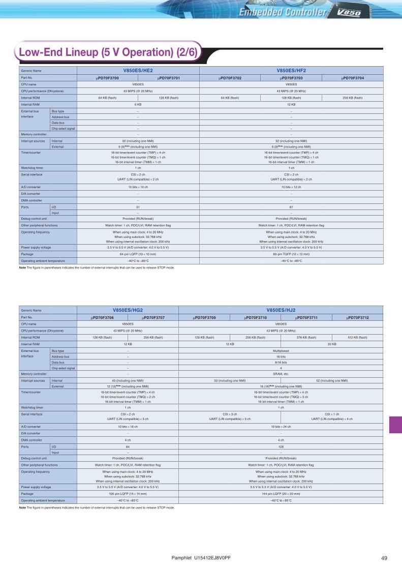
Pamphlet U15412EJ8V0PF ��
Low-End Lineup (5 V Operation) (2/6)Generic Name V850ES/HE2 V850ES/HF2Part No. mPD70F3700 mPD70F3701 mPD70F3702 mPD70F3703 mPD70F3704
CPU name V850ES V850ES
CPU performance (Dhrystone) 43 MIPS (@ 20 MHz) 43 MIPS (@ 20 MHz)
Internal ROM 64 KB (flash) 128 KB (flash) 64 KB (flash) 128 KB (flash) 256 KB (flash)
Internal RAM 6 KB 12 KB
External businterface
Bus type - -
Address bus - -
Data bus - -
Chip select signal - -
Memory controller - -
Interrupt sources Internal 32 (including one NMI) 32 (including one NMI)
External 9 (9)Note (including one NMI) 9 (9)Note (including one NMI)
Timer/counter 16-bit timer/event counter (TMP) × 4 ch16-bit timer/event counter (TMQ) × 1 ch
16-bit interval timer (TMM) × 1 ch
16-bit timer/event counter (TMP) × 4 ch16-bit timer/event counter (TMQ) × 1 ch
16-bit interval timer (TMM) × 1 ch
Watchdog timer 1 ch 1 ch
Serial interface CSI × 2 chUART (LIN compatible) × 2 ch
CSI × 2 chUART (LIN compatible) × 2 ch
A/D converter 10 bits × 10 ch 10 bits × 12 ch
D/A converter - -
DMA controller - -
Ports I/O 51 67
Input - -
Debug control unit Provided (RUN/break) Provided (RUN/break)
Other peripheral functions Watch timer: 1 ch, POC/LVI, RAM retention flag Watch timer: 1 ch, POC/LVI, RAM retention flag
Operating frequency When using main clock: 4 to 20 MHzWhen using subclock: 32.768 kHz
When using internal oscillation clock: 200 kHz
When using main clock: 4 to 20 MHzWhen using subclock: 32.768 kHz
When using internal oscillation clock: 200 kHz
Power supply voltage 3.5 V to 5.5 V (A/D converter: 4.0 V to 5.5 V) 3.5 V to 5.5 V (A/D converter: 4.0 V to 5.5 V)
Package 64-pin LQFP (10 × 10 mm) 80-pin TQFP (12 × 12 mm)
Operating ambient temperature -40°C to +85°C -40°C to +85°C
Note The figure in parentheses indicates the number of external interrupts that can be used to release STOP mode.
Generic Name V850ES/HG2 V850ES/HJ2Part No. mPD70F3706 mPD70F3707 mPD70F3709 mPD70F3710 mPD70F3711 mPD70F3712
CPU name V850ES V850ES
CPU performance (Dhrystone) 43 MIPS (@ 20 MHz) 43 MIPS (@ 20 MHz)
Internal ROM 128 KB (flash) 256 KB (flash) 128 KB (flash) 256 KB (flash) 376 KB (flash) 512 KB (flash)
Internal RAM 12 KB 12 KB 20 KB
External businterface
Bus type - Multiplexed
Address bus - 16 bits
Data bus - 8/16 bits
Chip select signal - 4
Memory controller - SRAM, etc.
Interrupt sources Internal 43 (including one NMI) 50 (including one NMI) 52 (including one NMI)
External 12 (12)Note (including one NMI) 16 (16)Note (including one NMI)
Timer/counter 16-bit timer/event counter (TMP) × 4 ch16-bit timer/event counter (TMQ) × 2 ch
16-bit interval timer (TMM) × 1 ch
16-bit timer/event counter (TMP) × 4 ch16-bit timer/event counter (TMQ) × 3 ch
16-bit interval timer (TMM) × 1 ch
Watchdog timer 1 ch 1 ch
Serial interface CSI × 2 chUART (LIN compatible) × 3 ch
CSI × 3 chUART (LIN compatible) × 3 ch
CSI × 1 chUART (LIN compatible) × 4 ch
A/D converter 10 bits × 16 ch 10 bits × 24 ch
D/A converter - -
DMA controller 4 ch 4 ch
Ports I/O 84 128
Input - -
Debug control unit Provided (RUN/break) Provided (RUN/break)
Other peripheral functions Watch timer: 1 ch, POC/LVI, RAM retention flag Watch timer: 1 ch, POC/LVI, RAM retention flag
Operating frequency When using main clock: 4 to 20 MHzWhen using subclock: 32.768 kHz
When using internal oscillation clock: 200 kHz
When using main clock: 4 to 20 MHzWhen using subclock: 32.768 kHz
When using internal oscillation clock: 200 kHz
Power supply voltage 3.5 V to 5.5 V (A/D converter: 4.0 V to 5.5 V) 3.5 V to 5.5 V (A/D converter: 4.0 V to 5.5 V)
Package 100-pin LQFP (14 × 14 mm) 144-pin LQFP (20 × 20 mm)
Operating ambient temperature -40°C to +85°C -40°C to +85°C
Note The figure in parentheses indicates the number of external interrupts that can be used to release STOP mode.

�0 Pamphlet U15412EJ8V0PF
Generic Name V850ES/KG2 V850ES/KJ2Part No. mPD70F3731 mPD70F3732 mPD70F3733 mPD70F3734
CPU name V850ES V850ES
CPU performance (Dhrystone) 43 MIPS (@ 20 MHz: 5 MHz × 4: 5 V operation) 43 MIPS (@ 20 MHz: 5 MHz × 4: 5 V operation)
Internal ROM 128 KB (flash) 256 KB (flash) 128 KB (flash) 256 KB (flash)
Internal RAM 6 KB 16 KB 6 KB 16 KB
External businterface
Bus type Multiplexed/separate Multiplexed/separate
Address bus 22 bits 24 bits
Data bus 8/16 bits 8/16 bits
Chip select signal 2 4
Memory controller SRAM, etc. SRAM, etc.
Interrupt sources Internal 41 (including two NMIs) 47 (including two NMIs)
External 9 (9)Note 1 (including one NMI) 9 (9)Note 1 (including one NMI)
Timer/counter 16-bit timer/event counter (TMO) × 4 ch16-bit timer/event counter (TMP) × 1 ch8-bit timer/event counter (TMH) × 2 ch8-bit timer/event counter (TM5) × 2 ch
8-bit interval timer (BRG) × 1 ch
16-bit timer/event counter (TMO) × 6 ch16-bit timer/event counter (TMP) × 1 ch8-bit timer/event counter (TMH) × 2 ch8-bit timer/event counter (TM5) × 2 ch
8-bit interval timer (BRG) × 1 ch
Watchdog timer 2 ch 2 ch
Serial interface CSI with automatic transfer function (32-byte buffer) × 2 chCSI × 2 ch
UART × 2 chI2C × 1 ch
UART/CSI × 1 ch
CSI with automatic transfer function (32-byte buffer) × 2 chCSI × 2 ch
UART/I2C × 1 chUART × 2 ch
I2C × 1 chUART/CSI × 1 ch
A/D converter 10 bits × 8 ch 10 bits × 16 ch
D/A converter 8 bits × 2 ch 8 bits × 2 ch
DMA controller 4 ch 4 ch
Ports I/O 76 112
Input 8 16
Debug control unit -Note 2 -Note 2 Provided (RUN/break)
Other peripheral functions Watch timer: 1 ch, real-time output Watch timer: 1 ch, real-time output
Operating frequency When using main clock: 2 to 20 MHzWhen using subclock: 32.768 kHz
When using main clock: 2 to 20 MHzWhen using subclock: 32.768 kHz
Power supply voltage 2.7 V to 5.5 V 2.7 V to 5.5 V
Package 100-pin LQFP (14 × 14 mm)100-pin QFP (14 × 20 mm)
144-pin LQFP (20 × 20 mm)
Operating ambient temperature -40°C to +85°C -40°C to +85°C
Notes 1. The figure in parentheses indicates the number of external interrupts that can be used to release STOP mode2. MINICUBE can be used by using a self-check board.
Generic Name V850ES/KE2 V850ES/KF2Part No. mPD70F3726 mPD70F3728 mPD70F3729
CPU name V850ES V850ES
CPU performance (Dhrystone) 43 MIPS (@ 20 MHz: 5 MHz × 4: 5 V operation) 43 MIPS (@ 20 MHz: 5 MHz × 4: 5 V operation)
Internal ROM 128 KB (flash) 128 KB (flash) 256 KB (flash)
Internal RAM 4 KB 6 KB 12 KB
External businterface
Bus type - Multiplexed
Address bus - 16 bits
Data bus - 8/16 bits
Chip select signal - 2
Memory controller - SRAM, etc.
Interrupt sources Internal 26 (including two NMIs) 29 (including two NMIs)
External 9 (9)Note 1 (including one NMI) 9 (9)Note 1 (including one NMI)
Timer/counter 16-bit timer/event counter (TMO) × 1 ch16-bit timer/event counter (TMP) × 1 ch8-bit timer/event counter (TMH) × 2 ch8-bit timer/event counter (TM5) × 2 ch
8-bit interval timer (BRG) × 1 ch
16-bit timer/event counter (TMO) × 2 ch16-bit timer/event counter (TMP) × 1 ch8-bit timer/event counter (TMH) × 2 ch8-bit timer/event counter (TM5) × 2 ch
8-bit interval timer (BRG) × 1 ch
Watchdog timer 2 ch 2 ch
Serial interface CSI × 2 chUART × 2 ch
I2C × 1 ch
CSI with automatic transfer function (32-byte buffer) × 1 chCSI × 2 ch
UART × 2 chI2C × 1 ch
A/D converter 10 bits × 8 ch 10 bits × 8 ch
D/A converter - -
DMA controller - -
Ports I/O 43 59
Input 8 8
Debug control unit -Note 2 -Note 2
Other peripheral functions Watch timer: 1 ch, real-time output Watch timer: 1 ch, real-time output
Operating frequency When using main clock: 2 to 20 MHzWhen using subclock: 32.768 kHz
When using main clock: 2 to 20 MHzWhen using subclock: 32.768 kHz
Power supply voltage 2.7 V to 5.5 V 2.7 V to 5.5 V
Package 64-pin LQFP (10 × 10 mm) 80-pin QFP (14 × 14 mm)
Operating ambient temperature -40°C to +85°C -40°C to +85°C
Notes 1. The figure in parentheses indicates the number of external interrupts that can be used to release STOP mode.2. MINICUBE can be used by using a self-check board.
Low-End Lineup (5 V Operation) (3/6)

Pamphlet U15412EJ8V0PF �1
Generic Name V850ES/KE1+ V850ES/KF1+Part No. mPD703302/3302Y mPD70F3302/F3302Y mPD70F3306/F3306Y mPD70F3308/F3308Y
CPU name V850ES V850ES
CPU performance (Dhrystone) 43 MIPS (@ 20 MHz: 5 MHz × 4: 5 V operation) 43 MIPS (@ 20 MHz: 5 MHz × 4: 5 V operation)
Internal ROM 128 KB (mask) 128 KB (flash) 128 KB (flash) 256 KB (flash)
Internal RAM 4 KB 6 KB 12 KB
External businterface
Bus type - Multiplexed
Address bus - 16 bits
Data bus - 8/16 bits
Chip select signal - 2
Memory controller - SRAM, etc.
Interrupt sources Internal 26 (Y products: 27) (including two NMIs) 29 (Y products: 30) (including two NMIs)
External 9 (9)Note 1 (including one NMI) 9 (9)Note 1 (including one NMI)
Timer/counter 16-bit timer/event counter (TMO) × 1 ch16-bit timer/event counter (TMP) × 1 ch
8-bit timer (TMH) × 2 ch, 8-bit timer/event counter (TM5) × 2 ch, 8-bit interval timer (BRG) × 1 ch
16-bit timer/event counter (TMO) × 2 ch16-bit timer/event counter (TMP) × 1 ch
8-bit timer (TMH) × 2 ch, 8-bit timer/event counter (TM5) × 2 ch, 8-bit interval timer (BRG) × 1 ch
Watchdog timer 2 ch 2 ch
Serial interface CSI × 2 chUART × 1 ch
UART (LIN compatible) × 1 chI2C × 1 chNote 2
CSI with automatic transfer function (32-byte buffer) × 1 chCSI × 2 ch
UART × 1 chUART (LIN compatible) × 1 ch
I2C × 1 chNote 2
A/D converter 10 bits × 8 ch 10 bits × 8 ch
D/A converter - -
DMA controller - -
Ports I/O 43 59
Input 8 8
Debug control unit -Note 3 -Note 3
Other peripheral functions Watch timer: 1 ch, ROM correction function: 4 points, POC/LVI/clock monitor, real-time output Watch timer: 1 ch, ROM correction function: 4 points, POC/LVI/clock monitor, real-time output
Operating frequency When using main clock: 2 to 20 MHzWhen using subclock: 32.768 kHz
When using internal oscillation clock: 240 kHz
When using main clock: 2 to 20 MHzWhen using subclock: 32.768 kHz
When using internal oscillation clock: 240 kHz
Power supply voltage 2.7 V to 5.5 V 2.7 V to 5.5 V
Package 64-pin TQFP (12 × 12 mm)64-pin LQFP (10 × 10 mm)
80-pin TQFP (12 × 12 mm)80-pin QFP (14 × 14 mm)
Operating ambient temperature -40°C to +85°C -40°C to +85°C
Notes 1. The figure in parentheses indicates the number of external interrupts that can be used to release STOP mode.2. Only Y products have an on-chip I2C interface.3. MINICUBE can be used by using a self-check board.
Generic Name V850ES/KG1+ V850ES/KJ1+Part No. mPD70F3311/F3311Y mPD703313/3313Y mPD70F3316/F3316Y mPD70F3318/F3318Y
mPD70F3313/F3313Y
CPU name V850ES V850ES
CPU performance (Dhrystone) 43 MIPS (@ 20 MHz: 5 MHz × 4: 5 V operation) 43 MIPS (@ 20 MHz: 5 MHz × 4: 5V operation)
Internal ROM 128 KB (flash) 256 KB (mask) 128 KB (flash) 256 KB (flash)
256 KB (flash)
Internal RAM 6 KB 16 KB 6 KB 16 KB
External businterface
Bus type Multiplexed/separate Multiplexed/separate
Address bus 22 bits 24 bits
Data bus 8/16 bits 8/16 bits
Chip select signal 2 4
Memory controller SRAM, etc. SRAM, etc.
Interrupt sources Internal 41 (Y products: 42) (including two NMIs) 46 (Y products: 48) (including two NMIs)
External 9 (9)Note 1 (including one NMI) 9 (9)Note 1 (including one NMI)
Timer/counter 16-bit timer/event counter (TMO) × 4 ch16-bit timer/event counter (TMP) × 1 ch
8-bit timer (TMH) × 2 ch, 8-bit timer/event counter (TM5) × 2 ch, 8-bit interval timer (BRG) × 1 ch
16-bit timer/event counter (TMO) × 6 ch16-bit timer/event counter (TMP) × 1 ch
8-bit timer (TMH) × 2 ch, 8-bit timer/event counter (TM5) × 2 ch, 8-bit interval timer (BRG) × 1 ch
Watchdog timer 2 ch 2 ch
Serial interface CSI with automatic transfer function (32-byte buffer) × 2 chCSI × 1 ch
UART/CSI × 1 chUART × 1 ch
UART (LIN compatible) × 1 chI2C × 1 chNote 2
CSI with automatic transfer function (32-byte buffer) × 2 chCSI × 2 ch
UARTNote 3/CSI × 1 chUARTNote 3/I2C × 1 chNote 2
UART (LIN compatible) × 1 chUART × 1 ch, I2C × 1 chNote 2
A/D converter 10 bits × 8 ch 10 bits × 16 ch
D/A converter 8 bits × 2 ch 8 bits × 2 ch
DMA controller 4 ch 4 ch
Ports I/O 76 112
Input 8 16
Debug control unit -Note 4 -Note 4 Provided (RUN/break)
Other peripheral functions Watch timer: 1 ch, ROM correction function: 4 points, POC/LVI/clock monitor, real-time output Watch timer: 1 ch, POC/LVI/clock monitor, real-time output
Operating frequency When using main clock: 2 to 20 MHzWhen using subclock: 32.768 kHz
When using internal oscillation clock: 240 kHz
When using main clock: 2 to 20 MHzWhen using subclock: 32.768 kHz
When using internal oscillation clock: 240 kHz
Power supply voltage 2.7 V to 5.5 V 2.7 V to 5.5 V
Package 100-pin LQFP (14 × 14 mm)100-pin QFP (14 × 20 mm)
144-pin LQFP (20 × 20 mm)
Operating ambient temperature -40°C to +85°C -40°C to +85°C
Notes 1. The figure in parentheses indicates the number of external interrupts that can be used to release STOP mode.2. Only Y products have an on-chip I2C interface.3. These UARTs are identical. Three UART channels are provided in KJ1+.4. MINICUBE can be used by using a self-check board.
Low-End Lineup (5 V Operation) (4/6)

�� Pamphlet U15412EJ8V0PF
Generic Name V853Part No. mPD703003A mPD703004A mPD703025A mPD70F3003A mPD70F3025A
CPU name V850
CPU performance (Dhrystone) 38 MIPS (@ 33 MHz)
Internal ROM 128 KB (mask) 96 KB (mask) 256 KB (mask) 128 KB (flash) 256 KB (flash)
Internal RAM 4 KB 8 KB 4 KB 8 KB
External businterface
Bus type Multiplexed
Address bus 20 bits
Data bus 16 bits
Chip select signal -
Memory controller SRAM, etc.
Interrupt sources Internal 32
External 17 (1)Note (including one NMI)
Timer/counter 16-bit timer/event counter × 4 ch16-bit interval timer × 1 ch
Watchdog timer -
Serial interface CSI × 2 chCSI/UART × 2 ch
A/D converter 10 bits × 8 ch
D/A converter 2 ch
DMA controller -
Ports I/O 67
Input 8
Debug control unit -
Other peripheral functions 12-bit PWM output × 2 ch
Operating frequency 2 to 33 MHz
Power supply voltage 4.5 V to 5.5 V
Package 100-pin LQFP (14 × 14 mm)
Operating ambient temperature -40°C to +85°C
Note The figure in parentheses indicates the number of external interrupts that can be used to release STOP mode.
Low-End Lineup (5 V Operation) (5/6)

Pamphlet U15412EJ8V0PF ��
Generic Name V850/SB1Part No. mPD703031BY mPD703033BY mPD70F3033BY mPD703030BY mPD70F3030BY mPD703032BY mPD70F3032BY
CPU name V850
CPU performance (Dhrystone) 23 MIPS (@ 20 MHz)
Internal ROM 128 KB (mask) 256 KB (mask) 256 KB (flash) 384 KB (mask) 384 KB (flash) 512 KB (mask) 512 KB (flash)
Internal RAM 8 KB 16 KB 24 KB
External businterface
Bus type Multiplexed/separate
Address bus 22 bits
Data bus 16 bits
Chip select signal -
Memory controller SRAM, etc.
Interrupt sources Internal 31 (Y products: 32) (including one NMI)
External 8 (6)Note (including one NMI)
Timer/counter 16-bit timer/event counter × 2 ch8-bit timer/event counter × 6 ch
8-bit timer × 2 ch
Watchdog timer 1 ch
Serial interface CSI × 1 chCSI/I2C × 2 ch
CSI/UART × 2 ch
A/D converter 10 bits × 12 ch
D/A converter -
DMA controller 6 ch (dedicated to internal RAM ↔ on-chip peripheral I/O)
Ports I/O 71
Input 12
Debug control unit -
Other peripheral functions ROM correction function: 4 points, Watch timer: 1 ch
Operating frequency When using main clock: 2 to 20 MHzWhen using subclock: 32.768 kHz
Power supply voltage 4.0 V to 5.5 V (A/D converter: 4.5 V to 5.5 V)
Package 100-pin LQFP (14 × 14 mm)100-pin QFP (14 × 20 mm)
100-pin QFP (14 × 20 mm)
Operating ambient temperature -40°C to +85°C
Note The figure in parentheses indicates the number of external interrupts that can be used to release STOP mode.
Generic Name V850/SC1 V850/SC1, V850/SC2, V850/SC3Part No. mPD703068Y mPD70F3089YNote 1
CPU name V850
CPU performance (Dhrystone) 23 MIPS (@ 20 MHz)
Internal ROM 512 KB (mask) 512 KB (flash)
Internal RAM 24 KB
External businterface
Bus type Multiplexed/separate
Address bus 22 bits
Data bus 16 bits
Chip select signal -
Memory controller SRAM, etc.
Interrupt sources Internal 42 (including one NMI) 49 (including one NMI)
External 11 (9)Note 2 (including one NMI)
Timer/counter 16-bit timer/event counter × 10 ch
Watchdog timer 1 ch
Serial interface CSI × 2 chCSI/I2C × 2 ch
CSI/UART × 2 chUART × 2 ch
A/D converter 10 bits × 12 ch
D/A converter -
DMA controller 6 ch (dedicated to internal RAM ↔ on-chip peripheral I/O)
Ports I/O 112
Input 12
Debug control unit -
Other peripheral functions ROM correction function: 4 pointsWatch timer: 1 ch
ROM correction function: 4 pointsWatch timer: 1 ch
IEBus controller: 1 chFCAN controller: 2 ch
Operating frequency When using main clock: 4 to 20 MHz (@ 5 V)When using subclock: 32.768 kHz
Power supply voltage 3.5 V to 5.5 V (A/D converter: 4.5 V to 5.5 V) 4.0 V to 5.5 V (A/D converter: 4.5 V to 5.5 V)
Package 144-pin LQFP (20 × 20 mm)
Operating ambient temperature -40°C to +85°C
Notes 1. mPD70F3089Y is a flash memory product common to V850/SC1, SC2, and SC3.2. The figure in parentheses indicates the number of external interrupts that can be used to release STOP mode.
Low-End Lineup (5 V Operation) (6/6)

�� Pamphlet U15412EJ8V0PF
Low-End Lineup (3 V Operation) (1/10)Generic Name V850ES/JG3-H (Under Development)Part No. mPD70F3760 mPD70F3761 mPD70F3762 mPD70F3770
CPU name V850ES
CPU performance (Dhrystone) 98 MIPS (@ 48 MHz)
Internal ROM 256 KB (flash) 384 KB (flash) 512 KB (flash) 256 KB (flash)
Internal RAM 40 KBNote 1 48 KBNote 1 56 KBNote 1 40 KBNote 1
External businterface
Bus type Multiplexed
Address bus 16 bits
Data bus 8/16 bits
Chip select signal 3
Memory controller SRAM, etc.
Interrupt sources Internal 69 (including one NMI) 73 (including one NMI)
External 17 (17)Note 2 (including one NMI)
Timer/counter 16-bit timer/event counter (TAA) × 6 ch16-bit timer/event counter (TAB) × 2 ch16-bit timer/event counter (TMT) × 1 ch
16-bit interval timer (TMM) × 4 ch
Watchdog timer 1 ch
Serial interface CSI × 2 ch UART (LIN compatible)/CSI × 2 ch UART (LIN compatible)/I2C × 2 ch
UART (LIN compatible)/CSI/I2C × 1 ch
CSI × 2 chUART (LIN compatible)/CSI × 2 chUART (LIN compatible)/I2C × 1 ch
UART (LIN compatible)/CSI/I2C × 1 chUART (LIN compatible)/I2C/aFCAN × 1 ch
A/D converter 10 bits × 12 ch
D/A converter 8 bits × 2 ch
DMA controller 4 ch
Ports I/O 77
Input -
Debug control unit Provided (RUN/break)
USB controller USB 2.0 function (full-speed) × 1 ch
Other peripheral functions Motor control function, real-time counter (RTC), real-time output, LVI/clock monitor, CRC, RAM retention flag
Operating frequency When using main clock: 3 to 48 MHzWhen using subclock: 32.768 kHz
When using internal oscillation clock: 220 kHz
Power supply voltage 2.85 V to 3.6 V (A/D converter, USB controller: 3.0 V to 3.6 V)
Package 100-pin LQFP (14 × 14 mm)
Operating ambient temperature -40°C to +85°C
Notes 1. 8 KB of data-only RAM included.2. The figure in parentheses indicates the number of external interrupts that can be used to release STOP mode.
Generic Name V850ES/JH3-H (Under Development)Part No. mPD70F3765 mPD70F3766 mPD70F3767 mPD70F3771
CPU name V850ES
CPU performance (Dhrystone) 98 MIPS (@ 48 MHz)
Internal ROM 256 KB (flash) 384 KB (flash) 512 KB (flash) 256 KB (flash)
Internal RAM 40 KBNote 1 48 KBNote 1 56 KBNote 1 40 KBNote 1
External businterface
Bus type Multiplexed/separate
Address bus 24 bits
Data bus 8/16 bits
Chip select signal 3
Memory controller SRAM, etc.
Interrupt sources Internal 69 (including one NMI) 73 (including one NMI)
External 20 (20)Note 2 (including one NMI)
Timer/counter 16-bit timer/event counter (TAA) × 6 ch16-bit timer/event counter (TAB) × 2 ch16-bit timer/event counter (TMT) × 1 ch
16-bit interval timer (TMM) × 4 ch
Watchdog timer 1 ch
Serial interface CSI × 2 chUART (LIN compatible)/CSI × 2 chUART (LIN compatible)/I2C × 2 ch
UART (LIN compatible)/CSI/I2C × 1 ch
CSI × 2 chUART (LIN compatible)/CSI × 2 chUART (LIN compatible)/I2C × 1 ch
UART (LIN compatible)/CSI/I2C × 1 chUART (LIN compatible)/I2C/aFCAN × 1 ch
A/D converter 10 bits × 12 ch
D/A converter 8 bits × 2 ch
DMA controller 4 ch
Ports I/O 96
Input -
Debug control unit Provided (RUN/break)
USB controller USB 2.0 function (full-speed) × 1 ch
Other peripheral functions Motor control function, real-time counter (RTC), real-time output, LVI/clock monitor, CRC, RAM retention flag
Operating frequency When using main clock: 3 to 48 MHzWhen using subclock: 32.768 kHz
When using internal oscillation clock: 220 kHz
Power supply voltage 2.85 V to 3.6 V (A/D converter, USB controller: 3.0 V to 3.6 V)
Package 128-pin LQFP (14 × 20 mm)
Operating ambient temperature -40°C to +85°C
Notes 1. 8 KB of data-only RAM included.2. The figure in parentheses indicates the number of external interrupts that can be used to release STOP mode.
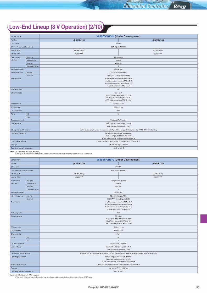
Pamphlet U15412EJ8V0PF ��
Generic Name V850ES/JG3-U (Under Development)Part No. mPD70F3763 mPD70F3764
CPU name V850ES
CPU performance (Dhrystone) 98 MIPS (@ 48 MHz)
Internal ROM 384 KB (flash) 512 KB (flash)
Internal RAM 48 KBNote 1 56 KBNote 1
External businterface
Bus type Multiplexed
Address bus 16 bits
Data bus 8/16 bits
Chip select signal 3
Memory controller SRAM, etc.
Interrupt sources Internal 72 (including one NMI)
External 15 (15)Note 2 (including one NMI)
Timer/counter 16-bit timer/event counter (TAA) × 6 ch16-bit timer/event counter (TAB) × 2 ch16-bit timer/event counter (TMT) × 1 ch
16-bit interval timer (TMM) × 4 ch
Watchdog timer 1 ch
Serial interface CSI × 2 ch UART (LIN compatible)/CSI × 2 ch UART (LIN compatible)/I2C × 2 ch
UART (LIN compatible)/CSI/I2C × 1 ch
A/D converter 10 bits × 12 ch
D/A converter 8 bits × 2 ch
DMA controller 4 ch
Ports I/O 75
Input -
Debug control unit Provided (RUN/break)
USB controller USB 2.0 function (full-speed) × 1 chUSB 2.0 host (full-speed) × 1 ch
Other peripheral functions Motor control function, real-time counter (RTC), real-time output, LVI/clock monitor, CRC, RAM retention flag
Operating frequency When using main clock: 3 to 48 MHzWhen using subclock: 32.768 kHz
When using internal oscillation clock: 220 kHz
Power supply voltage 2.85 V to 3.6 V (A/D converter, USB controller: 3.0 V to 3.6 V)
Package 100-pin LQFP (14 × 14 mm)
Operating ambient temperature -40°C to +85°C
Notes 1. 8 KB of data-only RAM included.2. The figure in parentheses indicates the number of external interrupts that can be used to release STOP mode.
Generic Name V850ES/JH3-U (Under Development)Part No. mPD70F3768 mPD70F3769
CPU name V850ES
CPU performance (Dhrystone) 98 MIPS (@ 48 MHz)
Internal ROM 384 KB (flash) 512 KB (flash)
Internal RAM 48 KBNote 1 56 KBNote 1
External businterface
Bus type Multiplexed/separate
Address bus 24 bits
Data bus 8/16 bits
Chip select signal 3
Memory controller SRAM, etc.
Interrupt sources Internal 72 (including one NMI)
External 20 (20)Note 2 (including one NMI)
Timer/counter 16-bit timer/event counter (TAA) × 6 ch16-bit timer/event counter (TAB) × 2 ch16-bit timer/event counter (TMT) × 1 ch
16-bit interval timer (TMM) × 4 ch
Watchdog timer 1 ch
Serial interface CSI × 2 chUART (LIN compatible)/CSI × 2 chUART (LIN compatible)/I2C × 2 ch
UART (LIN compatible)/CSI/I2C × 1 ch
A/D converter 10 bits × 12 ch
D/A converter 8 bits × 2 ch
DMA controller 4 ch
Ports I/O 96
Input -
Debug control unit Provided (RUN/break)
USB controller USB 2.0 function (full-speed) × 1 chUSB 2.0 host (full-speed) × 1 ch
Other peripheral functions Motor control function, real-time counter (RTC), real-time output, LVI/clock monitor, CRC, RAM retention flag
Operating frequency When using main clock: 3 to 48 MHzWhen using subclock: 32.768 kHz
When using internal oscillation clock: 220 kHz
Power supply voltage 2.85 V to 3.6 V (A/D converter, USB controller: 3.0 V to 3.6 V)
Package 128-pin LQFP (14 × 20 mm)
Operating ambient temperature -40°C to +85°C
Notes 1. 8 KB of data-only RAM included.2. The figure in parentheses indicates the number of external interrupts that can be used to release STOP mode.
Low-End Lineup (3 V Operation) (2/10)

�� Pamphlet U15412EJ8V0PF
Note The figure in parentheses indicates the number of external interrupts that can be used to release STOP mode.
Generic Name V850ES/JG3Part No. mPD70F3739 mPD70F3740 mPD70F3741 mPD70F3742
CPU name V850
CPU performance (Dhrystone) 69 MIPS (@ 32 MHz)
Internal ROM 384 KB (flash) 512 KB (flash) 768 KB (flash) 1024 KB (flash)
Internal RAM 32 KB 40 KB 60 KB 60 KB
External businterface
Bus type Multiplexed/separate
Address bus 22 bits
Data bus 8/16 bits
Chip select signal -
Memory controller SRAM, etc.
Interrupt sources Internal 48 (including one NMI)
External 9 (9)Note (including one NMI)
Timer/counter 16-bit interval timer (TMM) × 1 ch16-bit timer/event counter (TMP) × 6 ch16-bit timer/event counter (TMQ) × 1 ch
Watchdog timer 1 ch
Serial interface CSI × 3 chUART (LIN compatible)/CSI × 1 ch
CSI/I2C × 1 chUART (LIN compatible)/I2C × 2 ch
A/D converter 10 bits × 12 ch
D/A converter 8 bits × 2 ch
DMA controller 4 ch
Ports I/O 84
Input -
Debug control unit Provided (RUN/break)
Other peripheral functions Watch timer: 1 ch, real-time output, LVI/clock monitor, CRC, RAM retention flag
Operating frequency When using main clock: 2.5 to 32 MHzWhen using subclock: 32.768 kHz
When using internal oscillation clock: 220 kHz
Power supply voltage 2.85 V to 3.6 V (A/D converter: 3.0 V to 3.6 V)
Package 100-pin LQFP (14 × 14 mm)
Operating ambient temperature -40°C to +85°C
Generic Name V850ES/JJ3Part No. mPD70F3743 mPD70F3744 mPD70F3745 mPD70F3746
CPU name V850ES
CPU performance (Dhrystone) 69 MIPS (@ 32 MHz)
Internal ROM 384 KB (flash) 512 KB (flash) 768 KB (flash) 1024 KB (flash)
Internal RAM 32 KB 40 KB 60 KB
External businterface
Bus type Multiplexed/separate
Address bus 24 bits
Data bus 8/16 bits
Chip select signal 4
Memory controller SRAM, etc.
Interrupt sources Internal 61 (including one NMI)
External 10 (10)Note (including one NMI)
Timer/counter 16-bit interval timer (TMM) × 1 ch16-bit timer/event counter (TMP) × 9 ch16-bit timer/event counter (TMQ) × 1 ch
Watchdog timer 1 ch
Serial interface CSI × 4 chUART (LIN compatible)/CSI × 1 ch
CSI/I2C × 1 chUART (LIN compatible)/I2C × 2 ch
UART (LIN compatible) × 1 ch
A/D converter 10 bits × 16 ch
D/A converter 8 bits × 2 ch
DMA controller 4 ch
Ports I/O 128
Input -
Debug control unit Provided (RUN/break)
Other peripheral functions Watch timer: 1 ch, real-time output, LVI/clock monitor, CRC
Operating frequency When using main clock: 2.5 to 32 MHzWhen using subclock: 32.768 kHz
When using internal oscillation clock: 220 kHz
Power supply voltage 2.85 V to 3.6 V (A/D converter: 3.0 V to 3.6 V)
Package 144-pin LQFP (20 × 20 mm)
Operating ambient temperature -40°C to +85°C
Note The figure in parentheses indicates the number of external interrupts that can be used to release STOP mode.
Low-End Lineup (3 V Operation) (3/10)

Pamphlet U15412EJ8V0PF ��
Generic Name V850ES/JF3-L V850ES/JG3-LPart No. mPD70F3735 mPD70F3736 mPD70F3737 mPD70F3738
CPU name V850ES V850ES
CPU performance (Dhrystone) 43 MIPS (@ 20 MHz) 43 MIPS (@ 20 MHz)
Internal ROM 128 KB (flash) 256 KB (flash) 128 KB (flash) 256 KB (flash)
Internal RAM 8 KB 16 KB 8 KB 16 KB
External businterface
Bus type Multiplexed Multiplexed/separate
Address bus 18 bits 22 bits
Data bus 8/16 bits 8/16 bits
Chip select signal - -
Memory controller SRAM, etc. SRAM, etc.
Interrupt sources Internal 40 (including one NMI) 48 (including one NMI)
External 9 (9)Note (including one NMI) 9 (9)Note (including one NMI)
Timer/counter 16-bit timer/event counter (TMP) × 4 ch16-bit timer/event counter (TMQ) × 1 ch
16-bit interval timer (TMM) × 1 ch
16-bit timer/event counter (TMP) × 6 ch16-bit timer/event counter (TMQ) × 1 ch
16-bit interval timer (TMM) × 1 ch
Watchdog timer 1 ch 1 ch
Serial interface CSI × 2 chUART (LIN compatible) × 2 ch
CSI/I2C × 1 chUART (LIN compatible)/I2C × 1 ch
CSI × 3 chUART (LIN compatible)/CSI × 1 ch
CSI/I2C × 1 chUART (LIN compatible)/I2C × 2 ch
A/D converter 10 bits × 8 ch 10 bits × 12 ch
D/A converter 8 bits × 1 ch 8 bits × 2 ch
DMA controller 4 ch 4 ch
Ports I/O 66 84
Input - -
Debug control unit Provided (RUN/break) Provided (RUN/break)
Other peripheral functions Watch timer: 1 ch, real-time output, LVI/clock monitor, CRC Watch timer: 1 ch, real-time output, LVI/clock monitor, CRC
Operating frequency When using main clock: 2.5 to 20 MHzWhen using subclock: 32.768 kHz
When using internal oscillation clock: 220 kHz
When using main clock: 2.5 to 20 MHzWhen using subclock: 32.768 kHz
When using internal oscillation clock: 220 kHz
Power supply voltage 2.2 V to 3.6 V (A/D converter: 2.7 V to 3.6 V) 2.2 V to 3.6 V (A/D converter: 2.7 V to 3.6 V)
Package 80-pin LQFP (12 × 12 mm)80-pin LQFP (14 × 14 mm)
100-pin LQFP (14 × 14 mm)100-pin LQFP (14 × 20 mm)
Operating ambient temperature -40°C to +85°C -40°C to +85°C
Note The figure in parentheses indicates the number of external interrupts that can be used to release STOP mode.
Low-End Lineup (3 V Operation) (4/10)

�� Pamphlet U15412EJ8V0PF
Generic Name V850ES/JG2 Part No. mPD70F3715 mPD70F3716 mPD70F3717 mPD70F3718 mPD70F3719
CPU name V850ES
CPU performance (Dhrystone) 43 MIPS (@ 20 MHz)
Internal ROM 128 KB (flash) 256 KB (flash) 384 KB (flash) 512 KB (flash) 640 KB (flash)
Internal RAM 12 KB 24 KB 32 KB 40 KB 48 KB
External businterface
Bus type Multiplexed/separate
Address bus 22 bits
Data bus 8/16 bits
Chip select signal -
Memory controller SRAM, etc.
Interrupt sources Internal 48 (including one NMI)
External 9 (9)Note (including one NMI)
Timer/counter 16-bit interval timer (TMM) × 1 ch16-bit timer/event counter (TMP) × 6 ch16-bit timer/event counter (TMQ) × 1 ch
Watchdog timer 1 ch
Serial interface CSI × 3 chUART (LIN compatible)/CSI × 1 ch
CSI/I2C × 1 chUART (LIN compatible)/I2C × 2 ch
A/D converter 10 bits × 12 ch
D/A converter 8 bits × 2 ch
DMA controller 4 ch
Ports I/O 84
Input -
Debug control unit Provided (RUN/break)
Other peripheral functions Watch timer: 1 ch, real-time output, LVI/clock monitor
Operating frequency When using main clock: 2.5 to 20 MHzWhen using subclock: 32.768 kHz
When using internal oscillation clock: 200 kHz
Power supply voltage 2.85 V to 3.6 V (A/D converter: 3.0 V to 3.6 V)
Package 100-pin LQFP (14 × 14 mm)100-pin QFP (14 × 20 mm)
100-pin LQFP (14 × 14mm)
Operating ambient temperature -40°C to +85°C
Note The figure in parentheses indicates the number of external interrupts that can be used to release STOP mode.
Generic Name V850ES/JJ2 Part No. mPD70F3720 mPD70F3721 mPD70F3722 mPD70F3723 mPD70F3724
CPU name V850ES
CPU performance (Dhrystone) 43 MIPS (@ 20 MHz)
Internal ROM 128 KB (flash) 256 KB (flash) 384 KB (flash) 512 KB (flash) 640 KB (flash)
Internal RAM 12 KB 24 KB 32 KB 40 KB 48 KB
External businterface
Bus type Multiplexed/separate
Address bus 24 bits
Data bus 8/16 bits
Chip select signal 4
Memory controller SRAM, etc.
Interrupt sources Internal 61 (including one NMI)
External 10 (10)Note (including one NMI)
Timer/counter 16-bit interval timer (TMM) × 1 ch16-bit timer/event counter (TMP) × 9 ch16-bit timer/event counter (TMQ) × 1 ch
Watchdog timer 1 ch
Serial interface CSI × 4 chUART (LIN compatible)/CSI × 1 ch
CSI/I2C × 1 chUART (LIN compatible)/I2C × 2 ch
UART (LIN compatible) × 1 ch
A/D converter 10 bits × 16 ch
D/A converter 8 bits × 2 ch
DMA controller 4 ch
Ports I/O 128
Input -
Debug control unit Provided (RUN/break)
Other peripheral functions Watch timer: 1 ch, real-time output, LVI/clock monitor
Operating frequency When using main clock: 2.5 to 20 MHzWhen using subclock: 32.768 kHz
When using internal oscillation clock: 200 kHz
Power supply voltage 2.85 V to 3.6 V (A/D converter: 3.0 V to 3.6 V)
Package 144-pin LQFP (20 × 20 mm)
Operating ambient temperature -40°C to +85°C
Note The figure in parentheses indicates the number of external interrupts that can be used to release STOP mode.
Low-End Lineup (3 V Operation) (5/10)
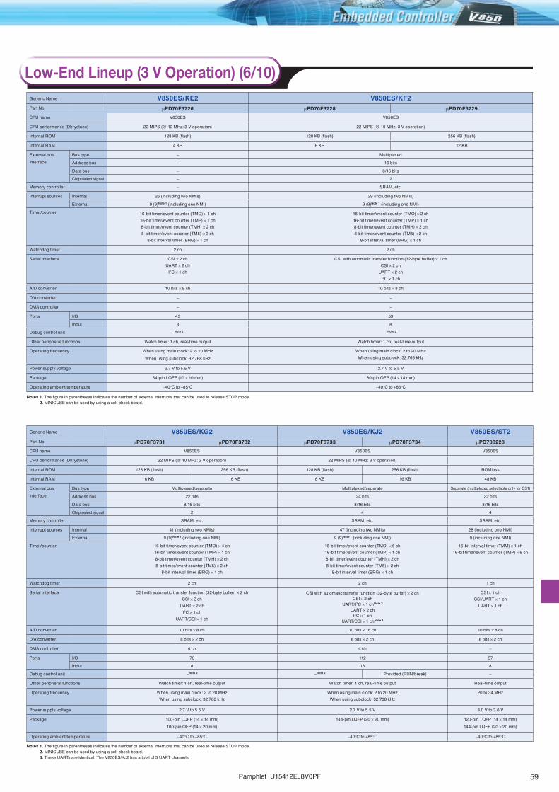
Pamphlet U15412EJ8V0PF ��
Generic Name V850ES/KE2 V850ES/KF2Part No. mPD70F3726 mPD70F3728 mPD70F3729
CPU name V850ES V850ES
CPU performance (Dhrystone) 22 MIPS (@ 10 MHz: 3 V operation) 22 MIPS (@ 10 MHz: 3 V operation)
Internal ROM 128 KB (flash) 128 KB (flash) 256 KB (flash)
Internal RAM 4 KB 6 KB 12 KB
External businterface
Bus type - Multiplexed
Address bus - 16 bits
Data bus - 8/16 bits
Chip select signal - 2
Memory controller - SRAM, etc.
Interrupt sources Internal 26 (including two NMIs) 29 (including two NMIs)
External 9 (9)Note 1 (including one NMI) 9 (9)Note 1 (including one NMI)
Timer/counter 16-bit timer/event counter (TMO) × 1 ch16-bit timer/event counter (TMP) × 1 ch8-bit timer/event counter (TMH) × 2 ch8-bit timer/event counter (TM5) × 2 ch
8-bit interval timer (BRG) × 1 ch
16-bit timer/event counter (TMO) × 2 ch16-bit timer/event counter (TMP) × 1 ch8-bit timer/event counter (TMH) × 2 ch8-bit timer/event counter (TM5) × 2 ch
8-bit interval timer (BRG) × 1 ch
Watchdog timer 2 ch 2 ch
Serial interface CSI × 2 chUART × 2 ch
I2C × 1 ch
CSI with automatic transfer function (32-byte buffer) × 1 chCSI × 2 ch
UART × 2 chI2C × 1 ch
A/D converter 10 bits × 8 ch 10 bits × 8 ch
D/A converter - -
DMA controller - -
Ports I/O 43 59
Input 8 8
Debug control unit -Note 2 -Note 2
Other peripheral functions Watch timer: 1 ch, real-time output Watch timer: 1 ch, real-time output
Operating frequency When using main clock: 2 to 20 MHzWhen using subclock: 32.768 kHz
When using main clock: 2 to 20 MHzWhen using subclock: 32.768 kHz
Power supply voltage 2.7 V to 5.5 V 2.7 V to 5.5 V
Package 64-pin LQFP (10 × 10 mm) 80-pin QFP (14 × 14 mm)
Operating ambient temperature -40°C to +85°C -40°C to +85°C
Notes 1. The figure in parentheses indicates the number of external interrupts that can be used to release STOP mode.2. MINICUBE can be used by using a self-check board.
Generic Name V850ES/KG2 V850ES/KJ2 V850ES/ST2Part No. mPD70F3731 mPD70F3732 mPD70F3733 mPD70F3734 mPD703220
CPU name V850ES V850ES V850ES
CPU performance (Dhrystone) 22 MIPS (@ 10 MHz: 3 V operation) 22 MIPS (@ 10 MHz: 3 V operation) -
Internal ROM 128 KB (flash) 256 KB (flash) 128 KB (flash) 256 KB (flash) ROMless
Internal RAM 6 KB 16 KB 6 KB 16 KB 48 KB
External businterface
Bus type Multiplexed/separate Multiplexed/separate Separate (multiplexed selectable only for CS1)
Address bus 22 bits 24 bits 22 bits
Data bus 8/16 bits 8/16 bits 8/16 bits
Chip select signal 2 4 4
Memory controller SRAM, etc. SRAM, etc. SRAM, etc.
Interrupt sources Internal 41 (including two NMIs) 47 (including two NMIs) 28 (including one NMI)
External 9 (9)Note 1 (including one NMI) 9 (9)Note 1 (including one NMI) 9 (including one NMI)
Timer/counter 16-bit timer/event counter (TMO) × 4 ch16-bit timer/event counter (TMP) × 1 ch8-bit timer/event counter (TMH) × 2 ch8-bit timer/event counter (TM5) × 2 ch
8-bit interval timer (BRG) × 1 ch
16-bit timer/event counter (TMO) × 6 ch16-bit timer/event counter (TMP) × 1 ch8-bit timer/event counter (TMH) × 2 ch8-bit timer/event counter (TM5) × 2 ch
8-bit interval timer (BRG) × 1 ch
16-bit interval timer (TMM) × 1 ch16-bit timer/event counter (TMP) × 6 ch
Watchdog timer 2 ch 2 ch 1 ch
Serial interface CSI with automatic transfer function (32-byte buffer) × 2 chCSI × 2 ch
UART × 2 chI2C × 1 ch
UART/CSI × 1 ch
CSI with automatic transfer function (32-byte buffer) × 2 chCSI × 2 ch
UART/I2C × 1 chNote 3
UART × 2 chI2C × 1 ch
UART/CSI × 1 chNote 3
CSI × 1 chCSI/UART × 1 ch
UART × 1 ch
A/D converter 10 bits × 8 ch 10 bits × 16 ch 10 bits × 8 ch
D/A converter 8 bits × 2 ch 8 bits × 2 ch 8 bits × 2 ch
DMA controller 4 ch 4 ch -
Ports I/O 76 112 57
Input 8 16 8
Debug control unit -Note 2 -Note 2 Provided (RUN/break) -
Other peripheral functions Watch timer: 1 ch, real-time output Watch timer: 1 ch, real-time output Real-time output
Operating frequency When using main clock: 2 to 20 MHzWhen using subclock: 32.768 kHz
When using main clock: 2 to 20 MHzWhen using subclock: 32.768 kHz
20 to 34 MHz
Power supply voltage 2.7 V to 5.5 V 2.7 V to 5.5 V 3.0 V to 3.6 V
Package 100-pin LQFP (14 × 14 mm)100-pin QFP (14 × 20 mm)
144-pin LQFP (20 × 20 mm) 120-pin TQFP (14 × 14 mm)144-pin LQFP (20 × 20 mm)
Operating ambient temperature -40°C to +85°C -40°C to +85°C -40°C to +85°C
Notes 1. The figure in parentheses indicates the number of external interrupts that can be used to release STOP mode.2. MINICUBE can be used by using a self-check board.3. These UARTs are identical. The V850ES/KJ2 has a total of 3 UART channels.
Low-End Lineup (3 V Operation) (6/10)

�0 Pamphlet U15412EJ8V0PF
Generic Name V850ES/SG2-H V850ES/SG2Part No. Without IEBus, aFCAN mPD703262HY mPD703263HY mPD70F3263HY mPD703260Y mPD703261Y mPD70F3261Y mPD703262Y mPD703263Y mPD70F3263Y
On-chip IEBus mPD703272HY mPD703273HY mPD70F3273HY mPD703270Y mPD703271Y mPD70F3271Y mPD703272Y mPD703273Y mPD70F3273Y
On-chip aFCAN mPD703282HY mPD703283HY mPD70F3283HY mPD703280Y mPD703281Y mPD70F3281Y mPD703282Y mPD703283Y mPD70F3283Y
CPU name V850ES V850ES
CPU performance (Dhrystone) 66 MIPS (@ 32 MHz) 43 MIPS (@ 20 MHz)
Internal ROM 512 KB (mask) 640 KB (mask) 640 KB (flash) 256 KB (mask) 384 KB (mask) 384 KB (flash) 512 KB (mask) 640 KB (mask) 640 KB (flash)
Internal RAM 40 KB 48 KB 24 KB 32 KB 40 KB 48 KB
External businterface
Bus type Multiplexed/separate Multiplexed/separate
Address bus 22 bits 22 bits
Data bus 8/16 bits 8/16 bits
Chip select signal - -
Memory controller SRAM, etc. SRAM, etc.
Interrupt sources Internal 47Note 1/51Note 2 (including one NMI for each) 48Note 1/52Note 2 (Including one NMI for each)
External 9 (9)Note 3 (including one NMI) 9 (9)Note 3 (including one NMI)
Timer/counter 16-bit interval timer (TMM) × 1 ch16-bit timer/event counter (TMP) × 6 ch16-bit timer/event counter (TMQ) × 1 ch
16-bit interval timer (TMM) × 1 ch16-bit timer/event counter (TMP) × 6 ch16-bit timer/event counter (TMQ) × 1 ch
Watchdog timer 1 ch 1 ch
Serial interface CSI × 3 chUART (LIN compatible)/CSI × 1 ch
CSI/I2C × 1 chUART (LIN compatible)/I2C × 2 ch
CSI × 3 chUART (LIN compatible)/CSI × 1 ch
CSI/I2C × 1 chUART (LIN compatible)/I2C × 2 ch
A/D converter 10 bits × 12 ch 10 bits × 12 ch
D/A converter 8 bits × 2 ch 8 bits × 2 ch
DMA controller 4 ch 4 ch
Ports I/O 84 84
Input - -
Debug control unit - Provided (RUN/break) - Provided (RUN/break) - Provided (RUN/break)
Other peripheral functions Watch timer: 1 chIEBus controller: 1 chNote 4
aFCAN controller: 1 chNote 5
ROM correction function: 4 pointsReal-time output
Clock monitor, CRC
Watch timer: 1 chIEBus controller: 1 chNote 6
aFCAN controller: 1 chNote 7
ROM correction function: 4 pointsReal-time output
LVI/clock monitor, CRC
Operating frequency When using main clock: 2.5 to 32 MHzWhen using subclock: 32.768 kHz
When using internal oscillation clock: 200 kHz
When using main clock: 2.5 to 20 MHzWhen using subclock: 32.768 kHz
When using internal oscillation clock: 200 kHz
Power supply voltage 3.0 V to 3.6 V (@ 32 MHz) 2.85 V to 3.6 V (A/D converter: 3.0 V to 3.6 V) (@ 20 MHz)
Package 100-pin LQFP (14 × 14mm) 100-pin LQFP (14 × 14 mm)100-pin QFP (14 × 20 mm)Note 8
Operating ambient temperature -40°C to +85°C -40°C to +85°C
Generic Name V850ES/SJ2-H V850ES/SJ2Part No. Without IEBus, aFCAN mPD703265HY mPD703266HY mPD70F3266HY mPD703264Y mPD70F3264Y mPD703265Y mPD703266Y mPD70F3266Y
On-chip IEBus mPD703275HY mPD703276HY mPD70F3276HY mPD703274Y mPD70F3274Y mPD703275Y mPD703276Y mPD70F3276Y
On-chip aFCAN
1 ch mPD703285HY mPD703286HY mPD70F3286HY mPD703284Y mPD70F3284Y mPD703285Y mPD703286Y mPD70F3286Y
2 ch mPD703287HY mPD703288HY mPD70F3288HY − − mPD703287Y mPD703288Y mPD70F3288Y
CPU name V850ES V850ES
CPU performance (Dhrystone) 66 MIPS (@ 32 MHz) 43 MIPS (@ 20 MHz)
Internal ROM 512 KB (mask) 640 KB (mask) 640 KB (flash) 384 KB (mask) 384 KB (flash) 512 KB (mask) 640 KB (mask) 640 KB (flash)
Internal RAM 40 KB 48 KB 32 KB 40 KB 48 KB
External businterface
Bus type Multiplexed/separate Multiplexed/separate
Address bus 24 bits 24 bits
Data bus 8/16 bits 8/16 bits
Chip select signal 4 4
Memory controller SRAM, etc. SRAM, etc.
Interrupt sources Internal 60Note 1/64Note 2/68Note 3 (including one NMI for each) 61Note 1/65Note 2/69Note 3 (including one NMI for each)
External 10 (10)Note 4 (including one NMI) 10 (10)Note 4 (including one NMI)
Timer/counter 16-bit interval timer (TMM) × 1 ch16-bit timer/event counter (TMP) × 9 ch16-bit timer/event counter (TMQ) × 1 ch
16-bit interval timer (TMM) × 1 ch16-bit timer/event counter (TMP) × 9 ch16-bit timer/event counter (TMQ) × 1 ch
Watchdog timer 1 ch 1 ch
Serial interface CSI × 4 chUART (LIN compatible)/CSI × 1 ch
CSI/I2C × 1 chUART (LIN compatible)/I2C × 2 ch
UART (LIN compatible) × 1 ch
CSI × 4 chUART (LIN compatible)/CSI × 1 ch
CSI/I2C × 1 chUART (LIN compatible)/I2C × 2 ch
UART (LIN compatible) × 1 ch
A/D converter 10 bits × 16 ch 10 bits × 16 ch
D/A converter 8 bits × 2 ch 8 bits × 2 ch
DMA controller 4 ch 4 ch
Ports I/O 128 128
Input - -
Debug control unit - Provided (RUN/break) - Provided (RUN/break) - Provided (RUN/break)
Other peripheral functions Watch timer: 1 chIEBus controller: 1 chNote 5
aFCAN controller: 1 chNote 6
aFCAN controller: 2 chNote 7
ROM correction function: 4 pointsReal-time output
Clock monitor, CRC
Watch timer: 1 chIEBus controller: 1 chNote 8
aFCAN controller: 1 chNote 9
aFCAN controller: 2 chNote 10
ROM correction function: 4 pointsReal-time output
LVI/clock monitor, CRC
Operating frequency When using main clock: 2.5 to 32 MHzWhen using subclock: 32.768 kHz
When using internal oscillation clock: 200 kHz
When using main clock: 2.5 to 20 MHzWhen using subclock: 32.768 kHz
When using internal oscillation clock: 200 kHz
Power supply voltage 3.0 V to 3.6 V (@ 32 MHz) 2.85 V to 3.6 V (A/D converter: 3.0 V to 3.6 V) (@ 20 MHz)
Package 144-pin LQFP (20 × 20mm) 144-pin LQFP (20 × 20 mm)
Operating ambient temperature -40°C to +85°C -40°C to +85°C
Notes 4. mPD703272HY/3273HY/F3273HY only5. mPD703282HY/3283HY/F3283HY only6. mPD703270Y/3271Y/F3271Y/3272Y/3273Y/F3273Y only
Notes 7. mPD703280Y/3281Y/F3281Y/3282Y/3283Y/F3283Y only8. mPD703260Y/3261Y/F3261Y/3270Y/3271Y/F3271Y only
Notes 1. Products without IEBus and aFCAN only2. Products with IEBus or aFCAN only3. Products with 2 ch aFCAN only4. The figure in parentheses indicates the number of external interrupts that can be used to release STOP mode.
Notes 5. mPD703275HY/3276HY/F3276HY only6. mPD703285HY/3286HY/F3286HY only7. mPD703287HY/3288HY/F3288HY only8. mPD703274Y/F3274Y/3275Y/3276Y/F3276Y only
Notes 9. mPD703284Y/F3284Y/3285Y/3286Y/F3286Y only10. mPD703287Y/3288Y/F3288Y only
Notes 1. Products without IEBus and aFCAN only2. Products with IEBus or aFCAN only3. The figure in parentheses indicates the number of external interrupts that can be used to release STOP mode.
Low-End Lineup (3 V Operation) (7/10)

Pamphlet U15412EJ8V0PF �1
Generic Name V850ES/SG1Part No. mPD703249Y
CPU name V850ES
CPU performance (Dhrystone) 43 MIPS (@ 20 MHz)
Internal ROM 256 KB (mask)
Internal RAM 12 KB
External businterface
Bus type Multiplexed/separate
Address bus 22 bits
Data bus 8/16 bits
Chip select signal -
Memory controller SRAM, etc.
Interrupt sources Internal 32 (including one NMI)
External 9 (9)Note (including one NMI)
Timer/counter 16-bit interval timer (TMM) × 1 ch16-bit timer/event counter (TMP) × 5 ch
Watchdog timer 1 ch
Serial interface CSI × 2 chCSI/I2C × 1 chUART × 2 ch
I2C × 1 ch
A/D converter 10 bits × 12 ch
D/A converter -
DMA controller -
Ports I/O 84
Input -
Debug control unit -
Other peripheral functions Watch timer: 1 ch, ROM correction function: 4 points, clock monitor
Operating frequency When using main clock: 2.5 to 20 MHzWhen using subclock: 32.768 kHz
When using internal oscillation clock: 200 kHz
Power supply voltage 2.85 V to 3.6 V (A/D converter: 3.0 V to 3.6 V)
Package 100-pin LQFP (14 × 14 mm)100-pin QFP (14 × 20 mm)
Operating ambient temperature -40°C to +85°C
Note The figure in parentheses indicates the number of external interrupts that can be used to release STOP mode.
Low-End Lineup (3 V Operation) (8/10)

�� Pamphlet U15412EJ8V0PF
Generic Name V850ES/SA2 V850ES/SA3Part No. mPD703200/3200Y mPD703201/3201Y mPD70F3201/F3201Y mPD703204/3204Y mPD70F3204/F3204Y
CPU name V850ES
CPU performance (Dhrystone) 43 MIPS (@ 20 MHz)
Internal ROM 128 KB (mask) 256 KB (mask) 256 KB (flash) 256 KB (mask) 256 KB (flash)
Internal RAM 8 KB 16 KB
External businterface
Bus type Multiplexed/separate
Address bus 22 bits 24 bits
Data bus 8/16 bits
Chip select signal 4
Memory controller SRAM, etc.
Interrupt sources Internal 30 (Y products: 31) (including one NMI) 31 (Y products: 32) (including one NMI)
External 8 (8)Note 1 (including one NMI)
Timer/counter 16-bit timer/event counter × 2 ch8-bit timer/event counter × 4 ch
Watchdog timer 1 ch
Serial interface CSI × 2 ch CSI × 3 ch
CSI/UART × 1 chCSI/I2C × 1 chNote 2
UART × 1 ch
A/D converter 10 bits × 12 ch 10 bits × 16 ch
D/A converter 8 bits × 2 ch
DMA controller 4 ch
Ports I/O 68 84
Input 14 18
Debug control unit -
Other peripheral functions ROM correction function: 4 points, real-time counter (watch timer): 1 ch
Operating frequency When using main clock: 2 to 20 MHzWhen using subclock: 32.768 kHz
Power supply voltage 2.2 V to 2.7 V
Package 100-pin TQFP (14 × 14 mm) 121-pin FBGA (12 × 12 mm)
Operating ambient temperature -40°C to +85°C
Notes 1. The figure in parentheses indicates the number of external interrupts that can be used to release STOP mode.2. Only Y products have an on-chip I2C interface.
Generic Name V850/SA1Part No. mPD703014B/3014BY mPD703015B/3015BY mPD70F3015B/F3015BY mPD703017A/3017AY mPD70F3017A/F3017AY
CPU name V850
CPU performance (Dhrystone) 23 MIPS (@ 20 MHz)
Internal ROM 64 KB (mask) 128 KB (mask) 128 KB (flash) 256 KB (mask) 256 KB (flash)
Internal RAM 4 KB 8 KB
External businterface
Bus type Multiplexed/separate
Address bus 22 bits
Data bus 16 bits
Chip select signal -
Memory controller SRAM, etc.
Interrupt sources Internal 24 (including one NMI)
External 8 (5)Note 1 (including one NMI)
Timer/counter 16-bit timer/event counter × 2 ch8-bit timer/event counter × 4 ch
Watchdog timer 1 ch
Serial interface CSI × 1 chCSI/I2C × 1 chNote 2
CSI/UART × 1 chUART × 1 ch
A/D converter 10 bits × 12 ch
D/A converter -
DMA controller 3 ch (dedicated to internal RAM ↔ on-chip peripheral I/O)
Ports I/O 72
Input 13
Debug control unit -
Other peripheral functions Watch timer: 1 ch
Operating frequency When using main clock: 2 to 20 MHzWhen using subclock: 32.768 kHz
Power supply voltage 3.0 V to 3.6 V (@ 20 MHz)2.7 V to 3.6 V (@ 17 MHz)
Package 100-pin LQFP (14 × 14 mm)121-pin FBGA (12 × 12 mm)
Operating ambient temperature -40°C to +85°C
Notes 1. The figure in parentheses indicates the number of external interrupts that can be used to release STOP mode.2. Only Y products have an on-chip I2C interface.
Low-End Lineup (3 V Operation) (9/10)

Pamphlet U15412EJ8V0PF ��
Generic Name V850ES/KE1+ V850ES/KF1+Part No. mPD703302/3302Y mPD70F3302/F3302Y mPD70F3306/F3306Y mPD70F3308/F3308Y
CPU name V850ES V850ES
CPU performance (Dhrystone) 22 MIPS (@ 10 MHz: 3 V operation) 22 MIPS (@ 10 MHz: 3 V operation)
Internal ROM 128 KB (mask) 128 KB (flash) 128 KB (flash) 256 KB (flash)
Internal RAM 4 KB 6 KB 12 KB
External businterface
Bus type - Multiplexed
Address bus - 16 bits
Data bus - 8/16 bits
Chip select signal - 2
Memory controller - SRAM, etc.
Interrupt sources Internal 26 (Y products: 27) (including two NMIs) 29 (Y products: 30) (including two NMIs)
External 9 (9)Note 1 (including one NMI) 9 (9)Note 1 (including one NMI)
Timer/counter 16-bit timer/event counter (TMO) × 1 ch16-bit timer/event counter (TMP) × 1 ch
8-bit timer (TMH) × 2 ch, 8-bit timer/event counter (TM5) × 2 ch, 8-bit interval timer (BRG) × 1 ch
16-bit timer/event counter (TMO) × 2 ch16-bit timer/event counter (TMP) × 1 ch
8-bit timer (TMH) × 2 ch, 8-bit timer/event counter (TM5) × 2 ch, 8-bit interval timer (BRG) × 1 ch
Watchdog timer 2 ch 2 ch
Serial interface CSI × 2 chUART × 1 ch
UART (LIN compatible) × 1 chI2C × 1 chNote 2
CSI with automatic transfer function (32-byte buffer) × 1 chCSI × 2 ch
UART × 1 chUART (LIN compatible) × 1 ch
I2C × 1 chNote 2
A/D converter 10 bits × 8 ch 10 bits × 8 ch
D/A converter - -
DMA controller - -
Ports I/O 43 59
Input 8 8
Debug control unit -Note 3 -Note 3
Other peripheral functions Watch timer: 1 ch, ROM correction function: 4 points, POC/LVI/clock monitor, real-time output Watch timer: 1 ch, ROM correction function: 4 points, POC/LVI/clock monitor, real-time output
Operating frequency When using main clock: 2 to 20 MHzWhen using subclock: 32.768 kHz
When using internal oscillation clock: 240 kHz
When using main clock: 2 to 20 MHzWhen using subclock: 32.768 kHz
When using internal oscillation clock: 240 kHz
Power supply voltage 2.7 V to 5.5 V 2.7 V to 5.5 V
Package 64-pin TQFP (12 × 12 mm)64-pin LQFP (10 × 10 mm)
80-pin TQFP (12 × 12 mm)80-pin QFP (14 × 14 mm)
Operating ambient temperature -40°C to +85°C -40°C to +85°C
Notes 1. The figure in parentheses indicates the number of external interrupts that can be used to release STOP mode.2. Only Y products have an on-chip I2C interface.3. MINICUBE can be used by using a self-check board.
Generic Name V850ES/KG1+ V850ES/KJ1+Part No. mPD70F3311/F3311Y mPD703313/3313Y mPD70F3316/F3316Y mPD70F3318/F3318Y
mPD70F3313/F3313Y
CPU name V850ES V850ES
CPU performance (Dhrystone) 22 MIPS (@ 10 MHz: 3 V operation) 22 MIPS (@ 10 MHz: 3 V operation)
Internal ROM 128 KB (flash) 256 KB (mask) 128 KB (flash) 256 KB (flash)
256 KB (flash)
Internal RAM 6 KB 16 KB 6 KB 16 KB
External businterface
Bus type Multiplexed/separate Multiplexed/separate
Address bus 22 bits 24 bits
Data bus 8/16 bits 8/16 bits
Chip select signal 2 4
Memory controller SRAM, etc. SRAM, etc.
Interrupt sources Internal 41 (Y products: 42) (including two NMIs) 46 (Y products: 48) (including two NMIs)
External 9 (9)Note 1 (including one NMI) 9 (9)Note 1 (including one NMI)
Timer/counter 16-bit timer/event counter (TMO) × 4 ch16-bit timer/event counter (TMP) × 1 ch
8-bit timer (TMH) × 2 ch, 8-bit timer/event counter (TM5) × 2 ch, 8-bit interval timer (BRG) × 1 ch
16-bit timer/event counter (TMO) × 6 ch16-bit timer/event counter (TMP) × 1 ch
8-bit timer (TMH) × 2 ch, 8-bit timer/event counter (TM5) × 2 ch, 8-bit interval timer (BRG) × 1 ch
Watchdog timer 2 ch 2 ch
Serial interface CSI with automatic transfer function (32-byte buffer) × 2 chCSI × 1 ch
UART/CSI × 1 chUART × 1 ch
UART (LIN compatible) × 1 chI2C × 1 chNote 2
CSI with automatic transfer function (32-byte buffer) × 2 chCSI × 2 ch
UARTNote 3/CSI × 1 chUARTNote 3/I2C × 1 chNote 2
UART (LIN compatible) × 1 chUART × 1 ch, I2C × 1 chNote 2
A/D converter 10 bits × 8 ch 10 bits × 16 ch
D/A converter 8 bits × 2 ch 8 bits × 2 ch
DMA controller 4 ch 4 ch
Ports I/O 76 112
Input 8 16
Debug control unit -Note 4 -Note 3 Provided (RUN/break)
Other peripheral functions Watch timer: 1 ch, ROM correction function: 4 points, POC/LVI/clock monitor, real-time output Watch timer: 1 ch, POC/LVI/clock monitor, real-time output
Operating frequency When using main clock: 2 to 20 MHzWhen using subclock: 32.768 kHz
When using internal oscillation clock: 240 kHz
When using main clock: 2 to 20 MHzWhen using subclock: 32.768 kHz
When using internal oscillation clock: 240 kHz
Power supply voltage 2.7 V to 5.5 V 2.7 V to 5.5 V
Package 100-pin LQFP (14 × 14 mm)100-pin QFP (14 × 20 mm)
144-pin LQFP (20 × 20 mm)
Operating ambient temperature -40°C to +85°C -40°C to +85°C
Notes 1. The figure in parentheses indicates the number of external interrupts that can be used to release STOP mode.2. Only Y products have an on-chip I2C interface.3. These UARTs are identical. Three UART channels are provided in KJ1+.4. MINICUBE can be used by using a self-check board.
Low-End Lineup (3 V Operation) (10/10)

�� Pamphlet U15412EJ8V0PF
High-End Lineup (1/2)Generic Name V850E/MA3 V850E2/ME3Part No. mPD703131BY mPD703132BY mPD703133BY mPD703134BY mPD70F3134BY mPD703136BY mPD703500
CPU name V850E1 V850E2
CPU performance (Dhrystone) 158 MIPS (@ 80 MHz) 432 MIPS (@ 200 MHz)
Internal ROM 256 KB (mask) 512 KB (mask) 512 KB (flash) 256 KB (mask) ROMless (instruction cache: 8 KB, data cache: 8 KB)
Internal RAM 16 KB 32 KB 16 KB 32 KB 8 KB instruction: 168 KB, data: 32 KB
External businterface
Bus type Multiplexed/separate Separate
Address bus 26 bits 26 bits
Data bus 8/16 bits 8/16/32 bits
Chip select signal 8 8
Memory controller SDRAM, SRAM, etc. SDRAM, SRAM, etc.
Interrupt sources Internal 41 (including one NMI) 59
External 26 (26)Note (including one NMI) 40 (including one NMI)
Timer/counter 16-bit interval timer (TMD) × 4 ch16-bit timer/event counter (TMP) × 3 ch
16-bit timer/event counter (TMQ) × 1 ch (inverter timer compatible)16-bit encoder counter/timer (TMENC) × 1 ch
16-bit timer/event counter (TMC) × 6 ch16-bit interval timer (TMD) × 4 ch
16-bit encoder counter/timer (TMENC) × 2 ch
Watchdog timer 1 ch -
Serial interface CSI/UART × 3 chUART/I2C × 1 ch
CSI (with FIFO) × 1 chCSI (with FIFO)/UART × 1 ch
UART × 1 ch
A/D converter 10 bits × 8 ch 10 bits × 8 ch
D/A converter 8 bits × 2 ch -
DMA controller 4 ch 4 ch
Ports I/O 101 77
Input 11 1
Debug control unit Provided (RUN/break) Provided (RUN/break/trace)
Other peripheral functions ROM correction function: 4 points USB (function) × 1 ch, SSCG, 16-bit PWM output × 2 ch
Operating frequency 5 to 80 MHz 100 to 200 MHz
Power supply voltage 2.3 V to 2.7 V (internal)/3.0 V to 3.6 V (external) 1.40 V to 1.65 V (internal)/3.0 V to 3.6 V (external)
Package 144-pin LQFP (20 × 20 mm)161-pin FBGA (13 × 13 mm)
176-pin QFP (24 × 24 mm)
Operating ambient temperature -40°C to +85°C -40°C to +80°C
Note The figure in parentheses indicates the number of external interrupts that can be used to release STOP mode.
Generic Name V850E/ME2Part No. mPD703111B-06 mPD703111B-10 mPD703111B-13 mPD703111B-15
CPU name V850E1
CPU performance (Dhrystone) 142 MIPS (@ 66 MHz) 215 MIPS (@ 100 MHz) 286 MIPS (@ 133 MHz) 325 MIPS (@ 150 MHz)
Internal ROM ROMless (instruction cache: 8 KB)
Internal RAM instruction: 128 KB, data: 16 KB
External businterface
Bus type Separate
Address bus 26 bits
Data bus 8/16/32 bits
Chip select signal 8
Memory controller SDRAM, SRAM, etc.
Interrupt sources Internal 59
External 40 (32)Note (including one NMI)
Timer/counter 16-bit timer/event counter (TMC) × 6 ch16-bit interval timer (TMD) × 4 ch
16-bit encoder counter/timer (TMENC) × 2 ch
Watchdog timer -
Serial interface CSI (with FIFO) × 1 chCSI (with FIFO)/UART × 1 ch
UART × 1 ch
A/D converter 10 bits × 8 ch
D/A converter -
DMA controller 4 ch
Ports I/O 77
Input 1
Debug control unit Provided (RUN/break/trace)
Other peripheral functions USB (function) × 1 ch, SSCG16-bit PWM output × 2 ch
Operating frequency 10 to 150 MHz
Power supply voltage 1.35 V to 1.65 V (internal)/3.0 V to 3.6 V (external) 1.40 V to 1.65 V (internal)/3.0 V to 3.6 V (external)
Package 176-pin LQFP (24 × 24 mm)
Operating ambient temperature -40°C to +85°C -40°C to +70°C
Note The figure in parentheses indicates the number of external interrupts that can be used to release STOP mode.

Pamphlet U15412EJ8V0PF ��
High-End Lineup (2/2)Generic Name V850E/MA1 V850E/MA2Part No. mPD703103A mPD703105A mPD703106A mPD703107A mPD70F3107A mPD703108
CPU name V850E1 V850E1
CPU performance (Dhrystone) - 103 MIPS (@ 50 MHz) -
Internal ROM ROMless 128 KB (mask) 256 KB (mask) 256 KB (flash) ROMless
Internal RAM 4 KB 10 KB 4 KB
External businterface
Bus type Separate Separate
Address bus 26 bits 25 bits
Data bus 8/16 bits 8/16 bits
Chip select signal 8 4
Memory controller SDRAM, SRAM, etc. SDRAM, SRAM, etc.
Interrupt sources Internal 33 23
External 25 (17)Note (including one NMI) 8 (4)Note (including one NMI)
Timer/counter 16-bit timer/event counter (TMC) × 4 ch16-bit interval timer (TMD) × 4 ch
16-bit timer/event counter (TMC) × 2 ch16-bit interval timer (TMD) × 4 ch
Watchdog timer - -
Serial interface CSI × 1 chCSI/UART × 2 ch
UART × 1 ch
CSI/UART × 2 ch
A/D converter 10 bits × 8 ch 10 bits × 4 ch
D/A converter - -
DMA controller 4 ch 4 ch
Ports I/O 106 74
Input 9 5
Debug control unit - -
Other peripheral functions 12-bit PWM output × 2 ch -
Operating frequency 4 to 50 MHz 4 to 40 MHz
Power supply voltage 3.0 V to 3.6 V 3.0 V to 3.6 V
Package 144-pin LQFP (20 × 20 mm) 144-pin LQFP (20 × 20 mm)161-pin FBGA (13 × 13 mm)
100-pin LQFP (14 × 14 mm)
Operating ambient temperature -40°C to +85°C -40°C to +85°C
Note The figure in parentheses indicates the number of external interrupts that can be used to release STOP mode.
Generic Name V850E/MS1 V850E/MS2Part No. External 3.3 V mPD703100A-33 mPD703101A-33 mPD703102A-33 mPD70F3102A-33 mPD703130
External 5 V mPD703100-33 mPD703101-33 mPD703102-33 mPD70F3102-33
CPU name V850E1 V850E1
CPU performance (Dhrystone) − 47 MIPS (@ 33 MHz) -
Internal ROM ROMless 96 KB (mask) 128 KB (mask) 128 KB (flash) ROMless
Internal RAM 4 KB 4 KB
External businterface
Bus type Separate Separate
Address bus 24 bits 24 bits
Data bus 8/16 bits 8/16 bits
Chip select signal 8 4
Memory controller EDO DRAM, SRAM, etc. EDO DRAM, SRAM, etc.
Interrupt sources Internal 47 35
External 25 (1)Note (including one NMI) 10 (1)Note (including one NMI)
Timer/counter 16-bit timer/event counter × 6 ch16-bit interval timer × 2 ch
16-bit timer/event counter × 4 ch16-bit interval timer × 2 ch
Watchdog timer - -
Serial interface CSI × 2 chCSI/UART × 2 ch
CSI/UART × 2 ch
A/D converter 10 bits × 8 ch 10 bits × 4 ch
D/A converter - -
DMA controller 4 ch 4 ch
Ports I/O 122 52
Input 9 5
Debug control unit - -
Other peripheral functions - -
Operating frequency 2 to 33 MHz 10 to 33 MHz
Power supply voltage 3.0 V to 3.6 V (internal/external) (A products)3.0 V to 3.6 V (internal)/4.5 V to 5.5 V (external) (non-A products)
3.0 V to 3.6 V (internal)/4.5 V to 5.5 V (external)
Package 144-pin LQFP (20 × 20 mm) 100-pin LQFP (14 × 14 mm)
Operating ambient temperature -40°C to +85°C -40°C to +85°C
Note The figure in parentheses indicates the number of external interrupts that can be used to release STOP mode.

�� Pamphlet U15412EJ8V0PF
ASSP Lineup (Inverter Control, etc.) (1/4)
Generic Name V850E/IG3 V850E/IF3Part No. mPD70F3453 mPD70F3454 mPD70F3451 mPD70F3452
CPU name V850E1 V850E1
CPU performance (Dhrystone) 131 MIPS (@ 64 MHz) 131 MIPS (@ 64 MHz)
Internal ROM 128 KB (flash) 256 KB (flash) 128 KB (flash) 256 KB (flash)
Internal RAM 8 KB 12 KB 8 KB 12 KB
External businterface
Bus type - Multiplexed/separate Note 1 -
Address bus - Multiplexed: 16 bits, separate: 8 bitsNote 1 -
Data bus - 8/16 bitsNote 1 -
Chip select signal - 2Note 1 -
Memory controller - SRAM, etc.Note 1 -
Interrupt sources Internal 75 (including one NMI) 74 (including one NMI)
External 21 (18)Note 2 15 (12)Note 2
Timer/counter 16-bit timer/event counter (TAB) × 2 ch (inverter timer compatible)
16-bit timer/event counter (TAA) × 3 ch16-bit timer/event counter (TMT) × 2 ch (encoder count function: 2 ch)
16-bit timer/counter (TAA) × 2 ch16-bit interval timer (TMM) × 4 ch
16-bit timer/event counter (TAB) × 2 ch (inverter timer compatible)
16-bit timer/event counter (TAA) × 3 ch16-bit timer/event counter (TMT) × 2 ch (encoder count function: 1 ch)
16-bit timer/counter (TAA) × 2 ch16-bit interval timer (TMM) × 4 ch
Watchdog timer 1 ch 1 ch
Serial interface CSI/UART (with FIFO) × 1 chCSI/UART × 2 chUART/I2C × 1 ch
CSI/UART (with FIFO) × 1 chCSI/UART × 2 chUART/I2C × 1 ch
A/D converter 12 bits × 5 ch, 2 units (conversion time: 2 ms)10 bits × 8 ch
12 bits × 5 ch, 2 units (conversion time: 2 ms)10 bits × 4 ch
D/A converter - -
DMA controller 4 ch 4 ch
Ports I/O 56 44
Input 8 4
Debug control unit Provided (RUN/break) -
Other peripheral functions Operational amplifier, comparator, software pull-up function, POC/LVI/clock monitor Operational amplifier, comparator, software pull-up function, POC/LVI/clock monitor
Operating frequency 4 to 64 MHz 4 to 64 MHz
Power supply voltage 3.5 V to 5.5 V (A/D converter: 4.0 V to 5.5 V)
3.5 V to 5.5 V (A/D converter: 4.0 V to 5.5 V)
Package 100-pin LQFP (14 × 14 mm)100-pin LQFP (14 × 20 mm)
161-pin FBGA (10 × 10 mm)Note 3
80-pin LQFP (14 × 14 mm)
Operating ambient temperature -40°C to +85°C -40°C to +85°C
Notes 1. mPD70F3454GC-8EA-A only2. The figure in parentheses indicates the number of external interrupts that can be used to release STOP mode.3. mPD70F3454F1-DA9-A only
Generic Name V850E/MA3Part No. mPD703131BY mPD703132BY mPD703133BY mPD703134BY mPD70F3134BY mPD703136BY
CPU name V850E1
CPU performance (Dhrystone) 158 MIPS (@ 80 MHz)
Internal ROM 256 KB (mask) 512 KB (mask) 512 KB (flash) 256 KB (mask)
Internal RAM 16 KB 32 KB 16 KB 32 KB 8 KB
External businterface
Bus type Multiplexed/separate
Address bus 26 bits
Data bus 8/16 bits
Chip select signal 8
Memory controller SDRAM, SRAM, etc.
Interrupt sources Internal 41 (including one NMI)
External 26 (26)Note (including one NMI)
Timer/counter 16-bit interval timer (TMD) × 4 ch16-bit timer/event counter (TMP) × 3 ch
16-bit timer/event counter (TMQ) × 1 ch (inverter timer compatible)16-bit encoder counter/timer (TMENC) × 1 ch
Watchdog timer 1 ch
Serial interface CSI/UART × 3 chUART/I2C × 1 ch
A/D converter 10 bits × 8 ch
D/A converter 8 bits × 2 ch
DMA controller 4 ch
Ports I/O 101
Input 11
Debug control unit Provided (RUN/break)
Other peripheral functions ROM correction function: 4 points
Operating frequency 5 to 80 MHz
Power supply voltage 2.3 V to 2.7 V (internal)/3.0 V to 3.6 V (external)
Package 144-pin LQFP (20 × 20 mm)161-pin FBGA (13 × 13 mm)
Operating ambient temperature -40°C to +85°C
Note The figure in parentheses indicates the number of external interrupts that can be used to release STOP mode.

Pamphlet U15412EJ8V0PF ��
Generic Name V850E/IA1 V850E/IA2Part No. mPD703116 mPD70F3116 mPD703114 mPD70F3114
CPU name V850E1 V850E1
CPU performance (Dhrystone) 103 MIPS (@ 50 MHz) 82 MIPS (@ 40 MHz)
Internal ROM 256 KB (mask) 256 KB (flash) 128 KB (mask) 128 KB (flash)
Internal RAM 10 KB 6 KB
External businterface
Bus type Multiplexed Multiplexed
Address bus 24 bits 22 bits
Data bus 8/16 bits 8/16 bits
Chip select signal 8 -
Memory controller SRAM, etc. SRAM, etc.
Interrupt sources Internal 45 42
External 20 (14)Note (including one NMI) 16 (12)Note (including one NMI)
Timer/counter 16-bit 3-phase sinusoidal PWM timer × 2 ch16-bit encoder counter/timer × 2 ch
16-bit timer/counter × 2 ch16-bit timer/event counter × 1 ch
16-bit interval timer × 1 ch
16-bit 3-phase sinusoidal PWM timer × 2 ch16-bit encoder counter/timer × 1 ch
16-bit timer/counter × 2 ch16-bit timer/event counter × 1 ch
16-bit interval timer × 1 ch
Watchdog timer - -
Serial interface CSI × 2 chUART × 3 ch
CSI × 1 chCSI/UART × 1 ch
UART × 1 ch
A/D converter 10 bits × 8 ch, 2 units 10 bits × 6 ch (A/D converter 0)10 bits × 8 ch (A/D converter 1)
D/A converter - -
DMA controller 4 ch 4 ch
Ports I/O 75 47
Input 8 6
Debug control unit - -
Other peripheral functions FCAN controller × 1 ch -
Operating frequency 4 to 50 MHz 4 to 40 MHz
Power supply voltage 3.0 V to 3.6 V (internal)4.5 V to 5.5 V (external)
4.5 V to 5.5 V (when internal regulator used)
Package 144-pin LQFP (20 × 20 mm) 100-pin QFP (14 × 20 mm)100-pin LQFP (14 × 14 mm)
Operating ambient temperature -40°C to +85°C (110°C version available) -40°C to +85°C
Note The figure in parentheses indicates the number of external interrupts that can be used to release STOP mode.
Generic Name V850E/IA4 V850E/IA3Part No. mPD703185 mPD703186 mPD70F3186 mPD703183 mPD70F3184
CPU name V850E1 V850E1
CPU performance (Dhrystone) 126 MIPS (@ 64 MHz) 126 MIPS (@ 64 MHz)
Internal ROM 128 KB (mask) 256 KB (mask) 256 KB (flash) 128 KB (mask) 256 KB (flash)
Internal RAM 6 KB 12 KB 6 KB 12 KB
External businterface
Bus type - -
Address bus - -
Data bus - -
Chip select signal - -
Memory controller - -
Interrupt sources Internal 53 (including one NMI) 49 (including one NMI)
External 8 (7)Note 7 (6)Note
Timer/counter 16-bit timer/event counter (TMQ) × 2 ch (inverter timer compatible)16-bit encoder counter/timer (TMENC) × 2 ch
16-bit timer/event counter (TMP) × 2 ch16-bit timer/counter (TMP) × 2 ch16-bit interval timer (TMM) × 1 ch
16-bit timer/event counter (TMQ) × 1 ch (inverter timer compatible)16-bit encoder counter/timer (TMENC) × 1 ch
16-bit timer/event counter (TMP) × 2 ch16-bit timer/event counter (TMQ) × 1 ch
16-bit timer/counter (TMP) × 2 ch16-bit interval timer (TMM) × 1 ch
Watchdog timer 1 ch 1 ch
Serial interface CSI × 1 chUART × 1 ch
CSI/UART × 1 ch
CSI × 1 chUART × 1 ch
CSI/UART × 1 ch
A/D converter 10 bits × 4 ch, 2 units (conversion time: 2 ms)8/10 bits × 8 ch
10 bits × 4 ch, 10 bits × 2 ch (conversion time: 2 ms)8/10 bits × 6 ch
D/A converter - -
DMA controller 4 ch 4 ch
Ports I/O 56 44
Input 8 6
Debug control unit - Provided (RUN/break) -
Other peripheral functions ROM correction function: 4 points, operational amplifier, comparator, software pull-up function
ROM correction function: 4 points, operational amplifier, comparator, software pull-up function
Operating frequency 4 to 64 MHz 4 to 64 MHz
Power supply voltage 2.3 V to 2.7 V (internal)/4.0 V to 5.5 V (external) (A/D converter: 4.5 V to 5.5 V)
2.3 V to 2.7 V (internal)/4.0 V to 5.5 V (external) (A/D converter: 4.5 V to 5.5 V)
Package 100-pin LQFP (14 × 14 mm)100-pin QFP (14 × 20 mm)
80-pin QFP (14 × 14 mm)
Operating ambient temperature -40°C to +85°C -40°C to +85°C
Note The figure in parentheses indicates the number of external interrupts that can be used to release STOP mode.
ASSP Lineup (Inverter Control, etc.) (2/4)

�� Pamphlet U15412EJ8V0PF
Generic Name V850ES/HG3 V850ES/HJ3Part No. mPD70F3752 mPD70F3755 mPD70F3757
CPU name V850ES V850ES
CPU performance (Dhrystone) 69 MIPS (@ 32 MHz) 69 MIPS (@ 32 MHz) 66 MIPS (@ 32 MHz)
Internal ROM 256 KB (flash) 256 KB (flash) 512 KB (flash)
Internal RAM 16 KB 16 KB 32 KB
External businterface
Bus type - Multiplexed
Address bus - 16 bits
Data bus - 8/16 bits
Chip select signal - 4
Memory controller - SRAM, etc.
Interrupt sources Internal 51 (including one NMI) 58 (including one NMI) 64 (including one NMI)
External 12 (12)Note 1 (including one NMI) 16 (16)Note 1 (including one NMI)
Timer/counter 16-bit timer/event counter (TAA) × 5 ch16-bit timer/event counter (TAB) × 2 ch
(inverter timer compatible)16-bit interval timer (TMM) × 1 ch
16-bit timer/event counter (TAA) × 5 ch16-bit timer/event counter (TAB) × 3 ch
(inverter timer compatible)16-bit interval timer (TMM) × 1 ch
Watchdog timer 1 ch 1 ch
Serial interface CSI × 2 chUART (LIN compatible) × 3 ch
I2C × 1 ch
CSI × 3 chUART (LIN compatible) × 3 ch
I2C × 1 ch
CSI × 1 chUART (LIN compatible) × 4 ch
UART (LIN compatible)/CSI × 2 chNote 2
UART (LIN compatible)/I2C × 1 ch
A/D converter 10 bits × 16 ch 10 bits × 24 ch
D/A converter - -
DMA controller 4 ch 4 ch
Ports I/O 84 128
Input - -
Debug control unit Provided (RUN/break) Provided (RUN/break)
Other peripheral functions Watch timer: 1 ch, POC/LVI/clock monitor, RAM retention flag, SSCG Watch timer: 1 ch, POC/LVI/clock monitor, RAM retention flag, SSCG
Operating frequency When using main clock: 4 to 32 MHzWhen using subclock: 32.768 kHz
When using high-speed internal oscillation clock: 8 MHzWhen using low-speed internal oscillation clock: 240 kHz
When using main clock: 4 to 32 MHzWhen using subclock: 32.768 kHz
When using high-speed internal oscillation clock: 8 MHzWhen using low-speed internal oscillation clock: 240 kHz
Power supply voltage 3.7 V to 5.5 V (A/D converter: 4.0 V to 5.5 V) 3.7 V to 5.5 V (A/D converter: 4.0 V to 5.5 V)
Package 100-pin LQFP (14 × 14 mm) 144-pin LQFP (20 × 20 mm)
Operating ambient temperature -40°C to +85°C -40°C to +85°C
Notes 1. The figure in parentheses indicates the number of external interrupts that can be used to release STOP mode.2. Two channels identical to independent UART are available. The V850ES/HJ3 has a total of 6 channels of UART.
Generic Name V850ES/HE3 V850ES/HF3Part No. mPD70F3747 mPD70F3750
CPU name V850ES V850ES
CPU performance (Dhrystone) 69 MIPS (@ 32 MHz) 69 MIPS (@ 32 MHz)
Internal ROM 128 KB (flash) 256 KB (flash)
Internal RAM 8 KB 16 KB
External businterface
Bus type - -
Address bus - -
Data bus - -
Chip select signal - -
Memory controller - -
Interrupt sources Internal 43 (including one NMI) 43 (including one NMI)
External 9 (9)Note (including one NMI) 9 (9)Note (including one NMI)
Timer/counter 16-bit timer/event counter (TAA) × 5 ch16-bit timer/event counter (TAB) × 1 ch
(inverter timer compatible)16-bit interval timer (TMM) × 1 ch
16-bit timer/event counter (TAA) × 5 ch16-bit timer/event counter (TAB) × 1 ch
(inverter timer compatible)16-bit interval timer (TMM) × 1 ch
Watchdog timer 1 ch 1 ch
Serial interface CSI × 2 chUART (LIN compatible) × 2 ch
I2C × 1 ch
CSI × 2 chUART (LIN compatible) × 2 ch
I2C × 1 ch
A/D converter 10 bits × 10 ch 10 bits × 12 ch
D/A converter - -
DMA controller 4 ch 4 ch
Ports I/O 51 67
Input - -
Debug control unit Provided (RUN/break) Provided (RUN/break)
Other peripheral functions Watch timer: 1 ch, POC/LVI/clock monitor, RAM retention flag, SSCG Watch timer: 1 ch, POC/LVI/clock monitor, RAM retention flag, SSCG
Operating frequency When using main clock: 4 to 32 MHzWhen using subclock: 32.768 kHz
When using high-speed internal oscillation clock: 8 MHzWhen using low-speed internal oscillation clock: 240 kHz
When using main clock: 4 to 32 MHzWhen using subclock: 32.768 kHz
When using high-speed internal oscillation clock: 8 MHzWhen using low-speed internal oscillation clock: 240 kHz
Power supply voltage 3.7 V to 5.5 V (A/D converter: 4.0 V to 5.5 V) 3.7 V to 5.5 V (A/D converter: 4.0 V to 5.5 V)
Package 64-pin LQFP (10 × 10 mm) 80-pin LQFP (12 × 12 mm)
Operating ambient temperature -40°C to +85°C -40°C to +85°C
Note The figure in parentheses indicates the number of external interrupts that can be used to release STOP mode.
ASSP Lineup (Inverter Control, etc.) (3/4)
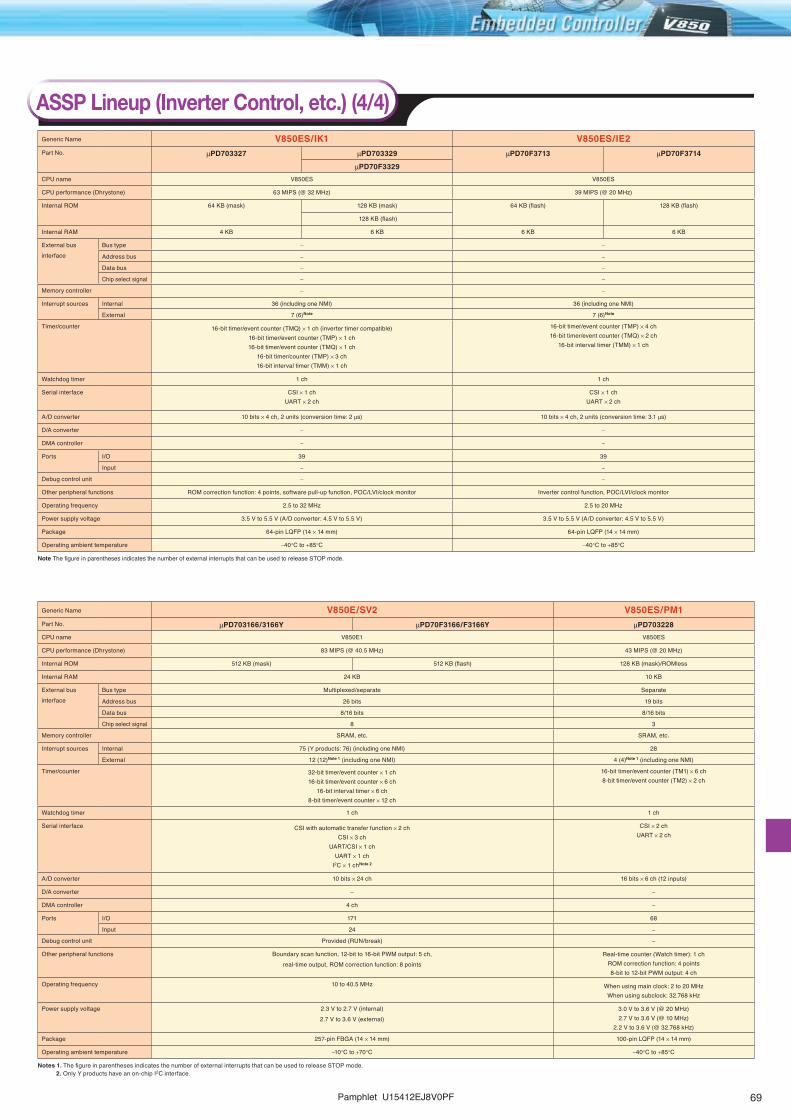
Pamphlet U15412EJ8V0PF ��
Generic Name V850E/SV2 V850ES/PM1Part No. mPD703166/3166Y mPD70F3166/F3166Y mPD703228
CPU name V850E1 V850ES
CPU performance (Dhrystone) 83 MIPS (@ 40.5 MHz) 43 MIPS (@ 20 MHz)
Internal ROM 512 KB (mask) 512 KB (flash) 128 KB (mask)/ROMless
Internal RAM 24 KB 10 KB
External businterface
Bus type Multiplexed/separate Separate
Address bus 26 bits 19 bits
Data bus 8/16 bits 8/16 bits
Chip select signal 8 3
Memory controller SRAM, etc. SRAM, etc.
Interrupt sources Internal 75 (Y products: 76) (including one NMI) 28
External 12 (12)Note 1 (including one NMI) 4 (4)Note 1 (including one NMI)
Timer/counter 32-bit timer/event counter × 1 ch16-bit timer/event counter × 6 ch
16-bit interval timer × 6 ch8-bit timer/event counter × 12 ch
16-bit timer/event counter (TM1) × 6 ch8-bit timer/event counter (TM2) × 2 ch
Watchdog timer 1 ch 1 ch
Serial interface CSI with automatic transfer function × 2 chCSI × 3 ch
UART/CSI × 1 chUART × 1 ch
I2C × 1 chNote 2
CSI × 2 chUART × 2 ch
A/D converter 10 bits × 24 ch 16 bits × 6 ch (12 inputs)
D/A converter - -
DMA controller 4 ch -
Ports I/O 171 68
Input 24 -
Debug control unit Provided (RUN/break) -
Other peripheral functions Boundary scan function, 12-bit to 16-bit PWM output: 5 ch,real-time output, ROM correction function: 8 points
Real-time counter (Watch timer): 1 chROM correction function: 4 points8-bit to 12-bit PWM output: 4 ch
Operating frequency 10 to 40.5 MHz When using main clock: 2 to 20 MHzWhen using subclock: 32.768 kHz
Power supply voltage 2.3 V to 2.7 V (internal)2.7 V to 3.6 V (external)
3.0 V to 3.6 V (@ 20 MHz)2.7 V to 3.6 V (@ 10 MHz)
2.2 V to 3.6 V (@ 32.768 kHz)
Package 257-pin FBGA (14 × 14 mm) 100-pin LQFP (14 × 14 mm)
Operating ambient temperature -10°C to +70°C -40°C to +85°C
Notes 1. The figure in parentheses indicates the number of external interrupts that can be used to release STOP mode.2. Only Y products have an on-chip I2C interface.
Generic Name V850ES/IK1 V850ES/IE2Part No. mPD703327 mPD703329 mPD70F3713 mPD70F3714
mPD70F3329
CPU name V850ES V850ES
CPU performance (Dhrystone) 63 MIPS (@ 32 MHz) 39 MIPS (@ 20 MHz)
Internal ROM 64 KB (mask) 128 KB (mask) 64 KB (flash) 128 KB (flash)
128 KB (flash)
Internal RAM 4 KB 6 KB 6 KB 6 KB
External businterface
Bus type - -
Address bus - -
Data bus - -
Chip select signal - -
Memory controller - -
Interrupt sources Internal 36 (including one NMI) 36 (including one NMI)
External 7 (6)Note 7 (6)Note
Timer/counter 16-bit timer/event counter (TMQ) × 1 ch (inverter timer compatible)16-bit timer/event counter (TMP) × 1 ch16-bit timer/event counter (TMQ) × 1 ch
16-bit timer/counter (TMP) × 3 ch16-bit interval timer (TMM) × 1 ch
16-bit timer/event counter (TMP) × 4 ch16-bit timer/event counter (TMQ) × 2 ch
16-bit interval timer (TMM) × 1 ch
Watchdog timer 1 ch 1 ch
Serial interface CSI × 1 chUART × 2 ch
CSI × 1 chUART × 2 ch
A/D converter 10 bits × 4 ch, 2 units (conversion time: 2 ms) 10 bits × 4 ch, 2 units (conversion time: 3.1 ms)
D/A converter - -
DMA controller - -
Ports I/O 39 39
Input - -
Debug control unit - -
Other peripheral functions ROM correction function: 4 points, software pull-up function, POC/LVI/clock monitor Inverter control function, POC/LVI/clock monitor
Operating frequency 2.5 to 32 MHz 2.5 to 20 MHz
Power supply voltage 3.5 V to 5.5 V (A/D converter: 4.5 V to 5.5 V) 3.5 V to 5.5 V (A/D converter: 4.5 V to 5.5 V)
Package 64-pin LQFP (14 × 14 mm) 64-pin LQFP (14 × 14 mm)
Operating ambient temperature -40°C to +85°C -40°C to +85°C
Note The figure in parentheses indicates the number of external interrupts that can be used to release STOP mode.
ASSP Lineup (Inverter Control, etc.) (4/4)

�0 Pamphlet U15412EJ8V0PF
ASSP Lineup (CAN) (1/9)
Generic Name V850E/DJ3 V850E/DL3Part No. mPD70F3424 mPD70F3425 mPD70F3426 mPD70F3427
CPU name V850E1 V850E1
CPU performance (Dhrystone) 126 MIPS (@ 64 MHz) 126 MIPS (@ 64 MHz)
Internal ROM 512 KB (flash) 1024 KB (flash) 2048 KB (flash) 1024 KB (flash)
Internal RAM 24 KB 32 KB 84 KB 60 KB
External businterface
Bus type - Separate
Address bus - 24 bits
Data bus - 8/16/32 bits
Chip select signal - 4
Memory controller - SRAM, etc.
Interrupt sources Internal 82 (including one NMI) 82 (including one NMI)
External 9 (9)Note (including one NMI) 9 (9)Note (including one NMI)
Timer/counter 16-bit timer/event counter (TMP) × 4 ch16-bit timer/event counter (TMG) × 3 ch
16-bit interval timer (TMZ) × 10 ch
16-bit timer/event counter (TMP) × 4 ch16-bit timer/event counter (TMG) × 3 ch
16-bit interval timer (TMZ) × 10 ch
Watchdog timer 1 ch 1 ch
Serial interface CSI × 3 chI2C × 2 ch
UART (LIN compatible) × 2 ch
CSI × 3 chI2C × 2 ch
UART (LIN compatible) × 2 ch
A/D converter 10 bits × 16 ch 10 bits × 16 ch
D/A converter - -
DMA controller 4 ch 4 ch
Ports I/O 98 101
Input 16 16
Debug control unit Provided (RUN/break) Provided (RUN/break)
Other peripheral functions Watch timer: 1 chMeter driver: 6 ch
ROM correction function: 8 points, POC/clock monitor, SSCGVoltage comparator
Sound generatorLCD bus interface
aFCAN controller: 2 ch
Watch timer: 1 chMeter driver: 6 ch
ROM correction function: 8 points, POC/clock monitorSSCG, Voltage comparator
Sound generatorLCD bus interface
aFCAN controller: 2 ch
Operating frequency When using main clock: 4 to 64 MHzWhen using subclock: 32.768 kHz
When using internal oscillation clock: 240 kHz
When using main clock: 4 to 64 MHzWhen using subclock: 32.768 kHz
When using internal oscillation clock: 240 kHz
Power supply voltage 3.2 V to 5.5 V (A/D converter: 3.5 V to 5.5 V) 3.2 V to 5.5 V (A/D converter: 3.5 V to 5.5 V)
Package 144-pin LQFP (20 × 20 mm) 208-pin LQFP (28 × 28 mm)
Operating ambient temperature -40°C to +85°C -40°C to +85°C
Note The figure in parentheses indicates the number of external interrupts that can be used to release STOP mode.
Generic Name V850E/DG3 (Under Development) V850E/DJ3Part No. mPD70F3416 mPD70F3417 mPD70F3421 mPD70F3422 mPD70F3423
CPU name V850E1 V850E1
CPU performance (Dhrystone) 34 MIPS (@ 16 MHz) 69 MIPS (@ 32 MHz)
Internal ROM 128 KB (flash) 256 KB (flash) 256 KB (flash) 384 KB (flash) 512 KB (flash)
Internal RAM 6 KB 12 KB 12 KB 16 KB 20 KB
External businterface
Bus type - -
Address bus - -
Data bus - -
Chip select signal - -
Memory controller - -
Interrupt sources Internal 48 (including one NMI) 75 (including one NMI)
External 5 (5)Note (including one NMI) 8 (8)Note (including one NMI)
Timer/counter 16-bit timer/event counter (TMP) × 1 ch16-bit timer/event counter (TMG) × 2 ch
16-bit interval timer (TMZ) × 4 ch
16-bit timer/event counter (TMP) × 4 ch16-bit timer/event counter (TMG) × 3 ch
16-bit interval timer (TMZ) × 6 ch
Watchdog timer 1 ch 1 ch
Serial interface CSI × 1 chI2C × 1 ch
UART (LIN compatible) × 2 ch
CSI × 2 chI2C × 2 ch
UART (LIN compatible) × 2 ch
A/D converter 10 bits × 8 ch 10 bits × 12 ch
D/A converter - -
DMA controller - 4 ch
Ports I/O 72 98
Input 8 16
Debug control unit - Provided (RUN/break)
Other peripheral functions Watch timer: 1 chMeter driver: 4 ch
ROM correction function: 6 points, POC/clock monitor, SSCGSound generator
LCD controller/driveraFCAN controller: 1 ch
Watch timer: 1 chMeter driver: 6 ch
ROM correction function: 8 points, POC/clock monitor, SSCGVoltage comparator
Sound generatorLCD controller/driver
aFCAN controller: 2 ch
Operating frequency When using main clock: 4 to 16 MHzWhen using subclock: 32.768 kHz
When using internal oscillation clock: 240 kHz
When using main clock: 4 to 32 MHzWhen using subclock: 32.768 kHz
When using internal oscillation clock: 240 kHz
Power supply voltage 3.2 V to 5.5 V (A/D converter: 3.5 V to 5.5 V) 3.2 V to 5.5 V (A/D converter: 3.5 V to 5.5 V)
Package 100-pin LQFP (14 × 14 mm) 144-pin LQFP (20 × 20 mm)
Operating ambient temperature -40°C to +85°C -40°C to +85°C
Note The figure in parentheses indicates the number of external interrupts that can be used to release STOP mode.

Pamphlet U15412EJ8V0PF �1
Generic Name V850ES/FE3 V850ES/FF3 V850ES/FG3Part No. mPD70F3370A mPD70F3371 mPD70F3372 mPD70F3373 mPD70F3374 mPD70F3375 mPD70F3376A mPD70F3377A
CPU name V850ES V850ES V850ES
CPU performance (Dhrystone) 69 MIPS (@ 32 MHz) 69 MIPS (@ 32 MHz) 69 MIPS (@ 32 MHz) 98 MIPS (@ 48 MHz)
Internal ROM 128 KB (flash) 256 KB (flash) 128 KB (flash) 256 KB (flash) 128 KB (flash) 256 KB (flash) 384 KB (flash) 512 KB (flash)
Internal RAM 8 KB 16 KB 8 KB 16 KB 8 KB 16 KB 24 KB 32 KB
EEPROM emulation 32 KB 32 KB 32 KB
External businterface
Bus type - - -
Address bus - - -
Data bus - - -
Chip select signal - - -
Memory controller - - -
Interrupt sources Internal 48 (including one NMI) 48 (including one NMI) 60 (including one NMI) 65 (including one NMI)
External 9 (9)Note (including one NMI) 9 (9)Note (including one NMI) 12 (12)Note (including one NMI) 13 (13)Note (including one NMI)
Timer/counter 16-bit timer/event counter (TAB) × 1 ch16-bit timer/event counter (TAA) × 5 ch
16-bit interval timer (TMM) × 1 ch
16-bit timer/event counter (TAB) × 1 ch16-bit timer/event counter (TAA) × 5 ch
16-bit interval timer (TMM) × 1 ch
16-bit timer/event counter (TAB) × 2 ch16-bit timer/event counter (TAA) × 5 ch
16-bit interval timer (TMM) × 1 ch
Watchdog timer 1 ch 1 ch 1 ch
Serial interface CSI × 2 chUART (LIN compatible) × 2 ch
I2C × 1 ch
CSI × 2 chUART (LIN compatible) × 2 ch
I2C × 1 ch
CSI × 2 chUART (LIN compatible) × 3 ch
I2C × 1 ch
CSI × 2 chUART (LIN compatible) × 5 ch
I2C × 1 ch
A/D converter 10 bits × 10 ch 10 bits × 12 ch 10 bits × 16 ch
D/A converter - - -
DMA controller 4 ch 4 ch 4 ch
Ports I/O 51 67 84
Input - - -
Debug control unit Provided (RUN/break) Provided (RUN/break) Provided (RUN/break)
Other peripheral functions Watch timer: 1 chaFCAN controller: 1 chKey input interrupt: 8 ch
Clock monitor/POC/LVI/PCL output, SSCG
Watch timer: 1 chaFCAN controller: 1 chKey input interrupt: 8 ch
Clock monitor/POC/LVI/PCL output, SSCG
Watch timer: 1 chaFCAN controller: 2 chKey input interrupt: 8 ch
Clock monitor/POC/LVI/PCL output, SSCG
Operating frequency When using main clock: 4 to 32 MHzWhen using subclock: 32.768 kHz
When using high-speed internal oscillation clock: 8 MHzWhen using low-speed internal oscillation clock: 240 kHz
When using main clock: 4 to 32 MHzWhen using subclock: 32.768 kHz
When using high-speed internal oscillation clock: 8 MHzWhen using low-speed internal oscillation clock: 240 kHz
When using main clock: 4 to 32 MHzWhen using subclock: 32.768 kHz
When using high-speed internal oscillation clock: 8 MHzWhen using low-speed internal oscillation clock: 240 kHz
When using main clock: 4 to 48 MHzWhen using subclock: 32.768 kHz
When using high-speed internal oscillation clock: 8 MHzWhen using low-speed internal oscillation clock: 240 kHz
Power supply voltage 3.3 V to 5.5 V (A/D converter: 4.0 V to 5.5 V) 3.3 V to 5.5 V (A/D converter: 4.0 V to 5.5 V) 3.3 V to 5.5 V (A/D converter: 4.0 V to 5.5 V)
Package 64-pin LQFP (10 × 10 mm) 80-pin LQFP (12 × 12 mm) 100-pin LQFP (14 × 14 mm)
Operating ambient temperature -40°C to +85°C, -40°C to +110°C, -40°C to +125°C -40°C to +85°C, -40°C to +110°C, -40°C to +125°C -40°C to +85°C, -40°C to +110°C, -40°C to +125°C
Note The figure in parentheses indicates the number of external interrupts that can be used to release STOP mode.
Generic Name V850ES/FJ3 V850ES/FK3Part No. mPD70F3378 mPD70F3379 mPD70F3380 mPD70F3381 mPD70F3382 mPD70F3383 mPD70F3384 mPD70F3385
CPU name V850ES V850ES
CPU performance (Dhrystone) 69 MIPS (@ 32 MHz) 98 MIPS (@ 48 MHz) 98 MIPS (@ 48 MHz)
Internal ROM 256 KB (flash) 384 KB (flash) 512 KB (flash) 768 KB (flash) 1024 KB (flash) 512 KB (flash) 768 KB (flash) 1024 KB (flash)
Internal RAM 16 KB 24 KB 32 KB 40 KB 48 KB 32 KB 48 KB 60 KB
EEPROM emulation 32 KB 32 KB
External businterface
Bus type Multiplexed Multiplexed
Address bus 16 bits 16 bits
Data bus 8/16 bits 8/16 bits
Chip select signal 4 4
Memory controller SRAM, etc. SRAM, etc.
Interrupt sources Internal 71 (including one NMI) 81 (including one NMI) 83 (including one NMI) 101 (including one NMI)
External 16 (16)Note 1 (including one NMI) 17 (17)Note 1 (including one NMI)
Timer/counter 16-bit timer/event counter (TAB) × 3 ch16-bit timer/event counter (TAA) × 5 ch
16-bit interval timer (TMM) × 1 ch
16-bit timer/event counter (TAB) × 3 ch16-bit timer/event counter (TAA) × 8 ch
16-bit interval timer (TMM) × 1 ch
Watchdog timer 1 ch 1 ch
Serial interface CSI × 3 chUART (LIN compatible) × 3 ch
I2C × 1 ch
CSI × 3 chUART (LIN compatible) × 6 ch
I2C × 1 ch
CSI × 4 chUART (LIN compatible) × 6 ch
I2C × 1 ch
CSI × 4 chUART (LIN compatible) × 8 ch
I2C × 1 ch
A/D converter 10 bits × 24 ch 10 bits × 24 ch, 10 bits × 16 ch
D/A converter - -
DMA controller 4 ch 4 ch
Ports I/O 128 152
Input - -
Debug control unit Provided (RUN/break) Provided (RUN/break)
Other peripheral functions Watch timer: 1 chaFCAN controller: 3 chNote 2
aFCAN controller: 4 chNote 3
Key input interrupt: 8 ch, clock monitor/POC/LVI/PCL output, SSCG
Watch timer: 1 chaFCAN controller: 5 chKey input interrupt: 8 ch
Clock monitor/POC/LVI/PCL output, SSCG
Operating frequency When using main clock: 4 to 32 MHzWhen using subclock: 32.768 kHzWhen using high-speed internal
oscillation clock: 8 MHzWhen using low-speed internal
oscillation clock: 240 kHz
When using main clock: 4 to 48 MHzWhen using subclock: 32.768 kHz
When using high-speed internal oscillation clock: 8 MHzWhen using low-speed internal oscillation clock: 240 kHz
When using main clock: 4 to 48 MHzWhen using subclock: 32.768 kHz
When using high-speed internal oscillation clock: 8 MHzWhen using low-speed internal oscillation clock: 240 kHz
Power supply voltage 3.3 V to 5.5 V (A/D converter: 4.0 V to 5.5 V) 3.3 V to 5.5 V (A/D converter: 4.0 V to 5.5 V)
Package 144-pin LQFP (20 × 20 mm) 176-pin LQFP (24 × 24 mm)
Operating ambient temperature -40°C to +85°C, -40°C to +110°C, -40°C to +125°C -40°C to +85°C, -40°C to +110°C, -40°C to +125°C
Notes 1. The figure in parentheses indicates the number of external interrupts that can be used to release STOP mode.2. mPD70F3378 only3. mPD70F3379/F3380/F3381/F3382 only
ASSP Lineup (CAN) (2/9)

�� Pamphlet U15412EJ8V0PF
Generic Name V850ES/FE3-LPart No. mPD70F3610 mPD70F3611 mPD70F3612 mPD70F3613 mPD70F3614
CPU name V850ES
CPU performance (Dhrystone) 43 MIPS (@ 20 MHz)
Internal ROM 64 KB (flash) 96 KB (flash) 128 KB (flash) 192 KB (flash) 256 KB (flash)
Internal RAM 6 KB 6 KB 8 KB 12 KB 16 KB
External businterface
Bus type -
Address bus -
Data bus -
Chip select signal -
Memory controller -
Interrupt sources Internal 39 (including one NMI)
External 9 (9)Note (including one NMI)
Timer/counter 16-bit timer/event counter (TAA) × 5 ch16-bit interval timer (TMM) × 1 ch
Watchdog timer 1 ch
Serial interface CSI × 2 chUART (LIN compatible) × 2 ch
I2C × 1 ch
A/D converter 10 bits × 10 ch
D/A converter -
DMA controller -
Ports I/O 51
Input -
Debug control unit Provided (RUN/break)
Other peripheral functions Watch timer: 1 chaFCAN controller: 1 chKey input interrupt: 8 ch
Clock monitor/POC/LVI/PCL output
Operating frequency When using main clock: 4 to 20 MHzWhen using subclock: 32.768 kHz
When using high-speed internal oscillation clock: 8 MHzWhen using low-speed internal oscillation clock: 240 kHz
Power supply voltage 3.3 V to 5.5 V (A/D converter: 4.0 V to 5.5 V)
Package 64-pin LQFP (10 × 10 mm)
Operating ambient temperature -40°C to +85°C, -40°C to +110°C, -40°C to +125°C
Note The figure in parentheses indicates the number of external interrupts that can be used to release STOP mode.
Generic Name V850ES/FF3-L V850ES/FG3-LPart No. mPD70F3615 mPD70F3616 mPD70F3617 mPD70F3618 mPD70F3619 mPD70F3620 mPD70F3621 mPD70F3622
CPU name V850ES V850ES
CPU performance (Dhrystone) 43 MIPS (@ 20 MHz) 43 MIPS (@ 20 MHz)
Internal ROM 64 KB (flash) 96 KB (flash) 128 KB (flash) 192 KB (flash) 256 KB (flash) 128 KB (flash) 192 KB (flash) 256 KB (flash)
Internal RAM 6 KB 6 KB 8 KB 12 KB 16 KB 8 KB 12 KB 16 KB
External businterface
Bus type - -
Address bus - -
Data bus - -
Chip select signal - -
Memory controller - -
Interrupt sources Internal 39 (including one NMI) 42 (including one NMI)
External 9 (9)Note (including one NMI) 12 (12)Note (including one NMI)
Timer/counter 16-bit timer/event counter (TAA) × 5 ch16-bit interval timer (TMM) × 1 ch
16-bit timer/event counter (TAA) × 5 ch16-bit interval timer (TMM) × 1 ch
Watchdog timer 1 ch 1 ch
Serial interface CSI × 2 chUART (LIN compatible) × 2 ch
I2C × 1 ch
CSI × 2 chUART (LIN compatible) × 3 ch
I2C × 1 ch
A/D converter 10 bits × 12 ch 10 bits × 16 ch
D/A converter - -
DMA controller - -
Ports I/O 67 84
Input - -
Debug control unit Provided (RUN/break) Provided (RUN/break)
Other peripheral functions Watch timer: 1 chaFCAN controller: 1 chKey input interrupt: 8 ch
Clock monitor/POC/LVI/PCL output
Watch timer: 1 chaFCAN controller: 1 chKey input interrupt: 8 ch
Clock monitor/POC/LVI/PCL output
Operating frequency When using main clock: 4 to 20 MHzWhen using subclock: 32.768 kHz
When using high-speed internal oscillation clock: 8 MHzWhen using low-speed internal oscillation clock: 240 kHz
When using main clock: 4 to 20 MHzWhen using subclock: 32.768 kHz
When using high-speed internal oscillation clock: 8 MHzWhen using low-speed internal oscillation clock: 240 kHz
Power supply voltage 3.3 V to 5.5 V (A/D converter: 4.0 V to 5.5 V) 3.3 V to 5.5 V (A/D converter: 4.0 V to 5.5 V)
Package 80-pin LQFP (12 × 12 mm) 100-pin LQFP (14 × 14 mm)
Operating ambient temperature -40°C to +85°C, -40°C to +110°C, -40°C to +125°C -40°C to +85°C, -40°C to +110°C, -40°C to +125°C
Note The figure in parentheses indicates the number of external interrupts that can be used to release STOP mode.
ASSP Lineup (CAN) (3/9)

Pamphlet U15412EJ8V0PF ��
Generic Name V850ES/FE2 V850ES/FF2Part No. mPD703230 mPD703231 mPD70F3231 mPD703232 mPD70F3232 mPD703233 mPD70F3233
CPU name V850ES V850ES
CPU performance (Dhrystone) 43 MIPS (@ 20 MHz) 43 MIPS (@ 20 MHz)
Internal ROM 64 KB (mask) 128 KB (mask) 128 KB (flash) 128 KB (mask) 128 KB (flash) 256 KB (mask) 256 KB (flash)
Internal RAM 4 KB 6 KB 6 KB 12 KB
External businterface
Bus type - -
Address bus - -
Data bus - -
Chip select signal - -
Memory controller - -
Interrupt sources Internal 36 (including one NMI) 36 (including one NMI)
External 9 (9)Note (including one NMI) 9 (9)Note (including one NMI)
Timer/counter 16-bit timer/event counter (TMP) × 4 ch16-bit timer/event counter (TMQ) × 1 ch
16-bit interval timer (TMM) × 1 ch
16-bit timer/event counter (TMP) × 4 ch16-bit timer/event counter (TMQ) × 1 ch
16-bit interval timer (TMM) × 1 ch
Watchdog timer 1 ch 1 ch
Serial interface CSI × 2 chUART (LIN compatible) × 2 ch
CSI × 2 chUART (LIN compatible) × 2 ch
A/D converter 10 bits × 10 ch 10 bits × 12 ch
D/A converter - -
DMA controller - -
Ports I/O 51 67
Input - -
Debug control unit - Provided (RUN/break) - Provided (RUN/break) - Provided (RUN/break)
Other peripheral functions Watch timer: 1 ch, POC/LVI, RAM retention flag, aFCAN controller: 1 ch Watch timer: 1 ch, POC/LVI, RAM retention flag, aFCAN controller: 1 ch
Operating frequency When using main clock: 4 to 20 MHz When using main clock: 4 to 20 MHz
Power supply voltage 3.5 V to 5.5 V 3.5 V to 5.5 V
Package 64-pin LQFP (10 × 10 mm) 80-pin TQFP (12 × 12 mm)
Operating ambient temperature -40°C to +85°C, -40°C to +110°C, -40°C to +125°C -40°C to +85°C, -40°C to +110°C, -40°C to +125°C
Note The figure in parentheses indicates the number of external interrupts that can be used to release STOP mode.
Generic Name V850ES/FG2 V850ES/FJ2Part No. mPD703234 mPD70F3234 mPD703235 mPD70F3235 mPD70F3236 mPD70F3237 mPD70F3238 mPD70F3239
CPU name V850ES V850ES
CPU performance (Dhrystone) 43 MIPS (@ 20 MHz) 43 MIPS (@ 20 MHz)
Internal ROM 128 KB (mask) 128 KB (flash) 256 KB (mask) 256 KB (flash) 384 KB (flash) 256 KB (flash) 376 KB (flash) 512 KB (flash)
Internal RAM 6 KB 12 KB 16 KB 12 KB 20 KB
External businterface
Bus type - Multiplexed
Address bus - 16 bits
Data bus - 8/16 bits
Chip select signal - 4
Memory controller - SRAM, etc.
Interrupt sources Internal 51 (including one NMI) 58 (including one NMI) 68 (including one NMI)
External 12 (12)Note (including one NMI) 16 (16)Note (including one NMI)
Timer/counter 16-bit timer/event counter (TMP) × 4 ch16-bit timer/event counter (TMQ) × 2 ch
16-bit interval timer (TMM) × 1 ch
16-bit timer/event counter (TMP) × 4 ch16-bit timer/event counter (TMQ) × 3 ch
16-bit interval timer (TMM) × 1 ch
Watchdog timer 1 ch 1 ch
Serial interface CSI × 2 chUART (LIN compatible) × 3 ch
CSI × 3 chUART (LIN compatible) × 3 ch
CSI × 3 chUART (LIN compatible) × 4 ch
A/D converter 10 bits × 16 ch 10 bits × 24 ch
D/A converter - -
DMA controller 4 ch 4 ch
Ports I/O 84 128
Input - -
Debug control unit - Provided (RUN/break) - Provided (RUN/break) Provided (RUN/break)
Other peripheral functions Watch timer: 1 ch, POC/LVI, RAM retention flag, aFCAN controller: 2 ch Watch timer: 1 ch, POC/LVI, RAM retention flag
aFCAN controller: 2 ch aFCAN controller: 4 ch
Operating frequency When using main clock: 4 to 20 MHz When using main clock: 4 to 20 MHz
Power supply voltage 3.5 V to 5.5 V 3.5 V to 5.5 V
Package 100-pin LQFP (14 × 14 mm) 144-pin LQFP (20 × 20 mm)
Operating ambient temperature -40°C to +85°C, -40°C to +110°C, -40°C to +125°C -40°C to +85°C, -40°C to +110°C, -40°C to +125°C
Note The figure in parentheses indicates the number of external interrupts that can be used to release STOP mode.
ASSP Lineup (CAN) (4/9)
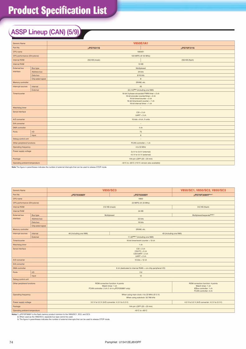
�� Pamphlet U15412EJ8V0PF
Generic Name V850E/IA1Part No. mPD703116 mPD70F3116
CPU name V850E1
CPU performance (Dhrystone) 103 MIPS (@ 50 MHz)
Internal ROM 256 KB (mask) 256 KB (flash)
Internal RAM 10 KB
External businterface
Bus type Multiplexed
Address bus 24 bits
Data bus 8/16 bits
Chip select signal 8
Memory controller SRAM, etc.
Interrupt sources Internal 45
External 20 (14)Note (including one NMI)
Timer/counter 16-bit 3-phase sinusoidal PWM timer × 2 ch16-bit encoder counter/timer × 2 ch
16-bit timer/counter × 2 ch16-bit timer/event counter × 1 ch
16-bit interval timer × 1 ch
Watchdog timer -
Serial interface CSI × 2 chUART × 3 ch
A/D converter 10 bits × 8 ch, 2 units
D/A converter -
DMA controller 4 ch
Ports I/O 75
Input 8
Debug control unit -
Other peripheral functions FCAN controller × 1 ch
Operating frequency 4 to 50 MHz
Power supply voltage 3.0 V to 3.6 V (internal)4.5 V to 5.5 V (external)
Package 144-pin LQFP (20 × 20 mm)
Operating ambient temperature -40°C to +85°C (110°C version also available)
Note The figure in parentheses indicates the number of external interrupts that can be used to release STOP mode.
Generic Name V850/SC3 V850/SC1, V850/SC2, V850/SC3Part No. mPD703088Y mPD703089Y mPD70F3089YNote 1
CPU name V850
CPU performance (Dhrystone) 23 MIPS (@ 20 MHz)
Internal ROM 512 KB (mask) 512 KB (flash)
Internal RAM 24 KB
External businterface
Bus type Multiplexed Multiplexed/separateNote 2
Address bus 22 bits
Data bus 16 bits
Chip select signal -
Memory controller SRAM, etc.
Interrupt sources Internal 46 (including one NMI) 49 (including one NMI)
External 11 (9)Note 3 (including one NMI)
Timer/counter 16-bit timer/event counter × 10 ch
Watchdog timer 1 ch
Serial interface CSI × 2 chCSI/I2C × 2 ch
CSI/UART × 2 chUART × 2 ch
A/D converter 10 bits × 12 ch
D/A converter -
DMA controller 6 ch (dedicated to internal RAM ↔ on-chip peripheral I/O)
Ports I/O 112
Input 12
Debug control unit -
Other peripheral functions ROM correction function: 4 pointsWatch timer: 1 ch
FCAN controller: 2 ch (1 ch in mPD703088Y only)
ROM correction function: 4 pointsWatch timer: 1 ch
IEBus controller: 1 chFCAN controller: 2 ch
Operating frequency When using main clock: 4 to 20 MHz (@ 5 V)When using subclock: 32.768 kHz
Power supply voltage 3.5 V to 5.5 V (A/D converter: 4.5 V to 5.5 V) 4.0 V to 5.5 V (A/D converter: 4.5 V to 5.5 V)
Package 144-pin LQFP (20 × 20 mm)
Operating ambient temperature -40°C to +85°C
Notes 1. mPD70F3089Y is the flash memory product common to the V850/SC1, SC2, and SC3.2. When used as the V850/SC3, separate bus type cannot be used.3. The figure in parentheses indicates the number of external interrupts that can be used to release STOP mode.
ASSP Lineup (CAN) (5/9)

Pamphlet U15412EJ8V0PF ��
Generic Name V850ES/SG1Part No. mPD703253Y
CPU name V850ES
CPU performance (Dhrystone) 43 MIPS (@ 20 MHz)
Internal ROM 128 KB (mask)
Internal RAM 8 KB
External businterface
Bus type Multiplexed/separate
Address bus 22 bits
Data bus 8/16 bits
Chip select signal -
Memory controller SRAM, etc.
Interrupt sources Internal 43 (including one NMI)
External 9 (9)Note (including one NMI)
Timer/counter 16-bit interval timer (TMM) × 1 ch16-bit timer/event counter (TMP) × 6 ch
Watchdog timer 1 ch
Serial interface CSI × 2 chCSI/I2C × 1 chUART × 2 ch
I2C × 1 ch
A/D converter 10 bits × 12 ch
D/A converter 8 bits × 2 ch
DMA controller 4 ch
Ports I/O 84
Input -
Debug control unit -
Other peripheral functions Watch timer: 1 ch, aFCAN controller: 1 chROM correction function: 4 points, clock monitor
Operating frequency When using main clock: 2.5 to 20 MHzWhen using subclock: 32.768 kHz
When using internal oscillation clock: 200 kHz
Power supply voltage 2.85 V to 3.6 V (A/D converter: 3.0 V to 3.6 V) (@ 20 MHz)
Package 100-pin LQFP (14 × 14 mm)
Operating ambient temperature -40°C to +85°C
Note The figure in parentheses indicates the number of external interrupts that can be used to release STOP mode.
Generic Name V850ES/JG3-H (Under Development) V850ES/JH3-H (Under Development)Part No. mPD70F3770 mPD70F3771
CPU name V850ES V850ES
CPU performance (Dhrystone) 98 MIPS (@ 48 MHz) 98 MIPS (@ 48 MHz)
Internal ROM 256 KB (flash) 256 KB (flash)
Internal RAM 40 KBNote 1 40 KBNote 1
External businterface
Bus type Multiplexed Multiplexed/separate
Address bus 16 bits 24 bits
Data bus 8/16 bits 8/16 bits
Chip select signal 3 3
Memory controller SRAM, etc. SRAM, etc.
Interrupt sources Internal 73 (including one NMI) 73 (including one NMI)
External 17 (17)Note 2 (including one NMI) 20 (20)Note 2 (including one NMI)
Timer/counter 16-bit timer/event counter (TAA) × 6 ch16-bit timer/event counter (TAB) × 2 ch16-bit timer/event counter (TMT) × 1 ch
16-bit interval timer (TMM) × 4 ch
16-bit timer/event counter (TAA) × 6 ch16-bit timer/event counter (TAB) × 2 ch16-bit timer/event counter (TMT) × 1 ch
16-bit interval timer (TMM) × 4 ch
Watchdog timer 1 ch 1 ch
Serial interface CSI × 2 chUART (LIN compatible)/CSI × 2 chUART (LIN compatible)/I2C × 1 ch
UART (LIN compatible)/CSI/I2C × 1 chUART (LIN compatible)/I2C/aFCAN × 1 ch
CSI × 2 chUART (LIN compatible)/CSI × 2 chUART (LIN compatible)/I2C × 1 ch
UART (LIN compatible)/CSI/I2C × 1 chUART (LIN compatible)/I2C/aFCAN × 1 ch
A/D converter 10 bits × 12 ch 10 bits × 12 ch
D/A converter 8 bits × 2 ch 8 bits × 2 ch
DMA controller 4 ch 4 ch
Ports I/O 77 96
Input - -
Debug control unit Provided (RUN/break) Provided (RUN/break)
USB controller USB 2.0 function (full-speed) × 1 ch USB 2.0 function (full-speed) × 1 ch
Other peripheral functions Motor control function, real-time counter (RTC), real-time output, LVI/clock monitor,CRC, RAM retention flag
Motor control function, real-time counter (RTC), real-time output, LVI/clock monitor,CRC, RAM retention flag
Operating frequency When using main clock: 3 to 48 MHzWhen using subclock: 32.768 kHz
When using internal oscillation clock: 220 kHz
When using main clock: 3 to 48 MHzWhen using subclock: 32.768 kHz
When using internal oscillation clock: 220 kHz
Power supply voltage 2.85 V to 3.6 V (A/D converter, USB controller: 3.0 V to 3.6 V) 2.85 V to 3.6 V (A/D converter, USB controller: 3.0 V to 3.6 V)
Package 100-pin LQFP (14 × 14 mm) 128-pin LQFP (14 × 20 mm)
Operating ambient temperature -40°C to +85°C -40°C to +85°C
Notes 1. 8 KB of data-only RAM included.2. The figure in parentheses indicates the number of external interrupts that can be used to release STOP mode.
ASSP Lineup (CAN) (6/9)

�� Pamphlet U15412EJ8V0PF
Generic Name V850ES/SG3Part No. mPD70F3335 mPD70F3336 mPD70F3350 mPD70F3351 mPD70F3352 mPD70F3353
CPU name V850ES
CPU performance (Dhrystone) 69 MIPS (@ 32 MHz)
Internal ROM 256 KB (flash) 384 KB (flash) 512 KB (flash) 640 KB (flash) 768 KB (flash) 1024 KB (flash)
Internal RAM 24 KB 32 KB 40 KB 48 KB 60 KB
External businterface
Bus type Multiplexed/separate
Address bus 22 bits
Data bus 8/16 bits
Chip select signal -
Memory controller SRAM, etc.
Interrupt sources Internal 52 (including one NMI)
External 9 (9)Note (including one NMI)
Timer/counter 16-bit interval timer (TMM) × 1 ch16-bit timer/event counter (TMP) × 6 ch16-bit timer/event counter (TMQ) × 1 ch
Watchdog timer 1 ch
Serial interface CSI × 3 chUART (LIN compatible)/CSI × 1 ch
CSI/I2C × 1 chUART (LIN compatible)/I2C × 2 ch
A/D converter 10 bits × 12 ch
D/A converter 8 bits × 2 ch
DMA controller 4 ch
Ports I/O 84
Input -
Debug control unit Provided (RUN/break)
Other peripheral functions Watch timer: 1 chIEBus controller/aFCAN controller: 1 ch
ROM correction function: 4 pointsReal-time output
LVI/clock monitor/CRC
Operating frequency When using main clock: 2.5 to 32 MHzWhen using subclock: 32.768 kHz
When using internal oscillation clock: 220 kHz
Power supply voltage 2.85 V to 3.6 V (A/D converter: 3.0 V to 3.6 V)
Package 100-pin LQFP (14 × 14 mm)
Operating ambient temperature -40°C to +85°C
Note The figure in parentheses indicates the number of external interrupts that can be used to release STOP mode.
Generic Name V850ES/SJ3Part No. On-chip aFCAN (1 ch max.) mPD70F3354 mPD70F3355 mPD70F3356 mPD70F3357 mPD70F3358
On-chip aFCAN (2 ch max.) mPD70F3364 mPD70F3365 mPD70F3366 mPD70F3367 mPD70F3368
CPU name V850ES
CPU performance (Dhrystone) 69 MIPS (@ 32 MHz)
Internal ROM 384 KB (flash) 512 KB (flash) 640 KB (flash) 768 KB (flash) 1024 KB (flash)
Internal RAM 32 KB 40 KB 48 KB 60 KB
External businterface
Bus type Multiplexed/separate
Address bus 24 bits
Data bus 8/16 bits
Chip select signal 4
Memory controller SRAM, etc.
Interrupt sources Internal 65Note 1/69Note 2 (including one NMI for each)
External 10 (10)Note 3 (including one NMI)
Timer/counter 16-bit interval timer (TMM) × 1 ch16-bit timer/event counter (TMP) × 9 ch16-bit timer/event counter (TMQ) × 1 ch
Watchdog timer 1 ch
Serial interface CSI × 4 chUART (LIN compatible)/CSI × 1 ch
CSI/I2C × 1 chUART (LIN compatible)/I2C × 2 ch
UART (LIN compatible) × 1 ch
A/D converter 10 bits × 16 ch
D/A converter 8 bits × 2 ch
DMA controller 4 ch
Ports I/O 128
Input -
Debug control unit Provided (RUN/break)
Other peripheral functions Watch timer: 1 chIEBus controller/aFCAN controllerNote 4: 1 ch
aFCAN controller: 2 chNote 5
ROM correction function: 4 pointsReal-time output
LVI/clock monitor/CRC
Operating frequency When using main clock: 2.5 to 32 MHzWhen using subclock: 32.768 kHz
When using internal oscillation clock: 220 kHz
Power supply voltage 2.85 V to 3.6 V (A/D converter: 3.0 V to 3.6 V)
Package 144-pin LQFP (20 × 20 mm)
Operating ambient temperature -40°C to +85°C
ASSP Lineup (CAN) (7/9)
Notes 4. mPD70F3354/F3355/F3356/F3357/F3358 only5. mPD70F3364/F3365/F3366/F3367/F3368 only
Notes 1. Product with 1 ch aFCAN only2. Products with 2 ch aFCAN only3. The figure in parentheses indicates the number of external interrupts that can be used to release STOP mode.

Pamphlet U15412EJ8V0PF ��
Generic Name V850E/SJ3-H (Under Development)Part No. On-chip aFCAN (1 ch max.) mPD70F3475 mPD70F3478
On-chip aFCAN (2 ch max.) mPD70F3476 mPD70F3479
CPU name V850E1
CPU performance (Dhrystone) 95 MIPS (@ 48 MHz)
Internal ROM 1280 KB (flash) 1536 KB (flash)
Internal RAM 92 KB (internal RAM: 60 KB, expanded internal RAM: 32 KB)
External businterface
Bus type Multiplexed/separate
Address bus 24 bits
Data bus 8/16 bits
Chip select signal 4
Memory controller SRAM, etc.
Interrupt sources Internal 99Note 1/103Note 2 (including one NMI for each)
External 11 (11)Note 3 (including one NMI)
Timer/counter 16-bit interval timer (TMM) × 3 ch16-bit timer/event counter (TMP) × 9 ch (encoder count function: 2 ch)
16-bit timer/event counter (TMQ) × 1 ch
Watchdog timer 1 ch
Serial interface UART/CSI × 1 ch, UART/I2C × 2 ch, UART/CSI/I2C × 1 ch, UART/CSI (FIFO compatible) × 1 ch, CSI/I2C × 1 ch, UART × 1 ch, UART (FIFO compatible) × 2 ch, CSI × 3 ch, CSI (FIFO compatible) × 1 ch, I2C × 2 ch
orUART/CSI × 1 ch, UART/I2C × 1 ch, UART/CSI/I2C × 2 ch, UART/CSI (FIFO compatible) × 1 ch,
CSI/I2C × 1 ch, UART × 1 ch, UART (FIFO compatible) × 2 ch, CSI × 2 ch, CSI (FIFO compatible) × 1 ch, I2C × 2 ch
A/D converter 10 bits × 16 ch
D/A converter 8 bits × 2 ch
DMA controller 4 ch
Ports I/O 128
Input -
Debug control unit Provided (RUN/break)
Other peripheral functions Watch timer: 1 chReal-time counter (Watch timer): 1 ch
IEBus controller/aFCAN controllerNote 4: 1 chaFCAN controller: 2 chNote 5
ROM correction function: 8 pointsReal-time output
LVI/clock monitor/CRC, SSCG
Operating frequency When using main clock: 48 MHz (max.)When using subclock: 32.768 kHz
When using internal oscillation clock: 220 kHz
Power supply voltage 2.85 V to 3.6 V (A/D converter, D/A converter: 3.0 V to 3.6 V)
Package 144-pin LQFP (20 × 20 mm)
Operating ambient temperature -40°C to +85°C
Notes 1. Products with 1 ch aFCAN only2. Products with 2 ch aFCAN only3. The figure in parentheses indicates the number of external interrupts that can be used to release STOP mode.
Notes 4. mPD70F3475, 70F34785. mPD70F3476, 70F3479
Generic Name V850E/SK3-H (Under Development)Part No. On-chip aFCAN (1 ch max.) mPD70F3481
On-chip aFCAN (2 ch max.) mPD70F3482
CPU name V850E1
CPU performance (Dhrystone) 95 MIPS (@ 48 MHz)
Internal ROM 1536 KB (flash)
Internal RAM 92 KB (internal RAM: 60 KB, expanded internal RAM: 32 KB)
External businterface
Bus type Multiplexed/separate
Address bus 24 bits
Data bus 8/16 bits
Chip select signal 4
Memory controller SRAM, etc.
Interrupt sources Internal 99Note 1/103Note 2 (including one NMI for each)
External 11 (11)Note 3 (including one NMI)
Timer/counter 16-bit interval timer (TMM) × 3 ch16-bit timer/event counter (TMP) × 9 ch (encoder count function: 2 ch)
16-bit timer/event counter (TMQ) × 1 ch
Watchdog timer 1 ch
Serial interface UART/CSI × 1 ch, UART/I2C × 2 ch, UART/CSI/I2C × 1 ch, UART/CSI (FIFO compatible) × 1 ch, CSI/I2C × 1 ch, UART × 1 ch, UART (FIFO compatible) × 2 ch, CSI × 3 ch, CSI (FIFO compatible) × 1 ch, I2C × 2 ch
orUART/CSI × 1 ch, CSI/I2C × 2 ch, UART × 5 ch, UART (FIFO compatible) × 2 ch, CSI × 3 ch, CSI (FIFO compatible) × 2 ch, I2C × 4 ch
A/D converter 10 bits × 16 ch
D/A converter 8 bits × 2 ch
DMA controller 4 ch
Ports I/O 156
Input -
Debug control unit Provided (RUN/break)
Other peripheral functions Watch timer: 1 chReal-time counter (Watch timer): 1 ch
IEBus controller/aFCAN controllerNote 4: 1 chaFCAN controller: 2 chNote 5
ROM correction function: 8 pointsReal-time output
LVI/clock monitor/CRC, SSCG
Operating frequency When using main clock: 48 MHz (max.)When using subclock: 32.768 kHz
When using internal oscillation clock: 220 kHz
Power supply voltage 2.85 V to 3.6 V (A/D converter, D/A converter: 3.0 V to 3.6 V)
Package 176-pin LQFP (24 × 24 mm)
Operating ambient temperature -40°C to +85°C
Notes 1. Products with 1 ch aFCAN only2. Products with 2 ch aFCAN only3. The figure in parentheses indicates the number of external interrupts that can be used to release STOP mode.
Notes 4. mPD70F34815. mPD70F3482
ASSP Lineup (CAN) (8/9)

�� Pamphlet U15412EJ8V0PF
Generic Name V850ES/SG2-H V850ES/SG2Part No. mPD703282HY mPD703283HY mPD70F3283HY mPD703280Y mPD703281Y mPD70F3281Y mPD703282Y mPD703283Y mPD70F3283Y
CPU name V850ES V850ES
CPU performance (Dhrystone) 66 MIPS (@ 32 MHz) 43 MIPS (@ 20 MHz)
Internal ROM 512 KB (mask) 640 KB (mask) 640 KB (flash) 256 KB (mask) 384 KB (mask) 384 KB (flash) 512 KB (mask) 640 KB (mask) 640 KB (flash)
Internal RAM 40 KB 48 KB 24 KB 32 KB 40 KB 48 KB
External businterface
Bus type Multiplexed/separate Multiplexed/separate
Address bus 22 bits 22 bits
Data bus 8/16 bits 8/16 bits
Chip select signal - -
Memory controller SRAM, etc. SRAM, etc.
Interrupt sources Internal 51 (including one NMI) 52 (including one NMI)
External 9 (9)Note (including one NMI) 9 (9)Note (including one NMI)
Timer/counter 16-bit interval timer (TMM) × 1 ch16-bit timer/event counter (TMP) × 6 ch16-bit timer/event counter (TMQ) × 1 ch
16-bit interval timer (TMM) × 1 ch16-bit timer/event counter (TMP) × 6 ch16-bit timer/event counter (TMQ) × 1 ch
Watchdog timer 1 ch 1 ch
Serial interface CSI × 3 chUART (LIN compatible)/CSI × 1 ch
CSI/I2C × 1 chUART (LIN compatible)/I2C × 2 ch
CSI × 3 chUART (LIN compatible)/CSI × 1 ch
CSI/I2C × 1 chUART (LIN compatible)/I2C × 2 ch
A/D converter 10 bits × 12 ch 10 bits × 12 ch
D/A converter 8 bits × 2 ch 8 bits × 2 ch
DMA controller 4 ch 4 ch
Ports I/O 84 84
Input - -
Debug control unit - Provided (RUN/break) - Provided (RUN/break) - Provided (RUN/break)
Other peripheral functions Watch timer: 1 chaFCAN controller: 1 ch
ROM correction function: 4 pointsReal-time output
Clock monitor/CRC
Watch timer: 1 chaFCAN controller: 1 ch
ROM correction function: 4 pointsReal-time output
LVI/clock monitor/CRC
Operating frequency When using main clock: 2.5 to 32 MHzWhen using subclock: 32.768 kHz
When using internal oscillation clock: 200 kHz
When using main clock: 2.5 to 20 MHzWhen using subclock: 32.768 kHz
When using internal oscillation clock: 200 kHz
Power supply voltage 3.0 V to 3.6 V 2.85 V to 3.6 V (A/D converter: 3.0 V to 3.6 V)
Package 100-pin LQFP (14 × 14 mm) 100-pin LQFP (14 × 14 mm)
Operating ambient temperature -40°C to +85°C -40°C to +85°CNote The figure in parentheses indicates the number of external interrupts that can be used to release STOP mode.
Generic Name V850ES/SJ2-H V850ES/SJ2Part No. On-chip
aFCAN1 ch mPD703285HY mPD703286HY mPD70F3286HY mPD703284Y mPD70F3284Y mPD703285Y mPD703286Y mPD70F3286Y
2 ch mPD703287HY mPD703288HY mPD70F3288HY − − mPD703287Y mPD703288Y mPD70F3288Y
CPU name V850ES V850ES
CPU performance (Dhrystone) 66 MIPS (@ 32 MHz) 43 MIPS (@ 20 MHz)
Internal ROM 512 KB (mask) 640 KB (mask) 640 KB (flash) 384 KB (mask) 384 KB (flash) 512 KB (mask) 640 KB (mask) 640 KB (flash)
Internal RAM 40 KB 48 KB 32 KB 40 KB 48 KB
External businterface
Bus type Multiplexed/separate Multiplexed/separate
Address bus 24 bits 24 bits
Data bus 8/16 bits 8/16 bits
Chip select signal 4 4
Memory controller SRAM, etc. SRAM, etc.
Interrupt sources Internal 64Note 1 /68Note 2 (including one NMI for each) 65Note 1/69Note 2 (including one NMI for each)
External 10 (10)Note 3 (including one NMI) 10 (10)Note 3 (including one NMI)
Timer/counter 16-bit interval timer (TMM) × 1 ch16-bit timer/event counter (TMP) × 9 ch16-bit timer/event counter (TMQ) × 1 ch
16-bit interval timer (TMM) × 1 ch16-bit timer/event counter (TMP) × 9 ch16-bit timer/event counter (TMQ) × 1 ch
Watchdog timer 1 ch 1 ch
Serial interface CSI × 4 chUART (LIN compatible)/CSI × 1 ch
CSI/I2C × 1 chUART (LIN compatible)/I2C × 2 ch
UART (LIN compatible) × 1 ch
CSI × 4 chUART (LIN compatible)/CSI × 1 ch
CSI/I2C × 1 chUART (LIN compatible)/I2C × 2 ch
UART (LIN compatible) × 1 ch
A/D converter 10 bits × 16 ch 10 bits × 16 ch
D/A converter 8 bits × 2 ch 8 bits × 2 ch
DMA controller 4 ch 4 ch
Ports I/O 128 128
Input - -
Debug control unit - Provided (RUN/break) - Provided (RUN/break) - Provided (RUN/break)
Other peripheral functions Watch timer: 1 chaFCAN controller: 1 chNote 4 aFCAN controller: 2 chNote 5
ROM correction function: 4 pointsReal-time output
Clock monitor/CRC
Watch timer: 1 chaFCAN controller: 1 chNote 6
aFCAN controller: 2 chNote 7
ROM correction function: 4 pointsReal-time output
LVI/clock monitor/CRC
Operating frequency When using main clock: 2.5 to 32 MHzWhen using subclock: 32.768 kHz
When using internal oscillation clock: 200 kHz
When using main clock: 2.5 to 20 MHzWhen using subclock: 32.768 kHz
When using internal oscillation clock: 200 kHz
Power supply voltage 3.0 V to 3.6 V 2.85 V to 3.6 V (A/D converter: 3.0 V to 3.6 V)
Package 144-pin LQFP (20 × 20 mm) 144-pin LQFP (20 × 20 mm)
Operating ambient temperature -40°C to +85°C -40°C to +85°C
Notes 1. Products with 1 ch aFCAN only2. Products with 2 ch aFCAN only3. The figure in parentheses indicates the number of external interrupts that can be used to release STOP mode.
Notes 4. mPD703285HY/3286HY/F3286HY only5. mPD703287HY/3288HY/F3288HY only6. mPD703284Y/F3284Y/3285Y/3286Y/F3286Y only7. mPD703287Y/3288Y/F3288Y only
ASSP Lineup (CAN) (9/9)

Pamphlet U15412EJ8V0PF ��
ASSP Lineup (IEBus) (1/5)Generic Name V850ES/SG1Part No. mPD703252Y
CPU name V850ES
CPU performance (Dhrystone) 43 MIPS (@ 20 MHz)
Internal ROM 256 KB (mask)
Internal RAM 12 KB
External businterface
Bus type Multiplexed/separate
Address bus 22 bits
Data bus 8/16 bits
Chip select signal -
Memory controller SRAM, etc.
Interrupt sources Internal 36 (including one NMI)
External 9 (9)Note (including one NMI)
Timer/counter 16-bit interval timer (TMM) × 1 ch16-bit timer/event counter (TMP) × 5 ch
Watchdog timer 1 ch
Serial interface CSI × 2 chCSI/I2C × 1 chUART × 2 ch
I2C × 1 ch
A/D converter 10 bits × 12 ch
D/A converter -
DMA controller -
Ports I/O 84
Input -
Debug control unit -
Other peripheral functions Watch timer: 1 ch, IEBus controller: 1 chROM correction function: 4 points, clock monitor
Operating frequency When using main clock: 2.5 to 20 MHzWhen using subclock: 32.768 kHz
When using internal oscillation clock: 200 kHz
Power supply voltage 2.85 V to 3.6 V (A/D converter: 3.0 V to 3.6 V)
Package 100-pin LQFP (14 × 14 mm)100-pin QFP (14 × 20 mm)
Operating ambient temperature -40°C to +85°C
Note The figure in parentheses indicates the number of external interrupts that can be used to release STOP mode.
Generic Name V850/SC2 V850/SC1, V850/SC2, V850/SC3Part No. mPD703069Y mPD70F3089YNote 1
CPU name V850
CPU performance (Dhrystone) 22 MIPS (@ 19 MHz) 23 MIPS (@ 20 MHz)
Internal ROM 512 KB (mask) 512 KB (flash)
Internal RAM 24 KB
External businterface
Bus type Multiplexed/separate
Address bus 22 bits
Data bus 16 bits
Chip select signal -
Memory controller SRAM, etc.
Interrupt sources Internal 44 (including one NMI) 49 (including one NMI)
External 11 (9)Note 2 (including one NMI)
Timer/counter 16-bit timer/event counter × 10 ch
Watchdog timer 1 ch
Serial interface CSI × 2 chCSI/I2C × 2 ch
CSI/UART × 2 chUART × 2 ch
A/D converter 10 bits × 12 ch
D/A converter -
DMA controller 6 ch (dedicated to internal RAM ↔ on-chip peripheral I/O)
Ports I/O 112
Input 12
Debug control unit -
Other peripheral functions ROM correction function: 4 pointsWatch timer: 1 ch, IEBus controller: 1 ch
ROM correction function: 4 points, watch timer: 1 chIEBus controller: 1 ch, FCAN controller: 2 ch
Operating frequency When using main clock: 4 to 19 MHz (@ 5 V)When using subclock: 32.768 kHz
When using main clock: 4 to 20 MHz (@ 5 V)When using subclock: 32.768 kHz
Power supply voltage 3.5 V to 5.5 V (A/D converter: 4.5 V to 5.5 V)
4.0 V to 5.5 V (A/D converter: 4.5 V to 5.5 V)
Package 144-pin LQFP (20 × 20 mm)
Operating ambient temperature -40°C to +85°C
Notes 1. mPD70F3089Y is the flash memory product common to the V850/SC1, SC2, and SC3.2. The figure in parentheses indicates the number of external interrupts that can be used to release STOP mode.

�0 Pamphlet U15412EJ8V0PF
Generic Name V850/SB2Part No. mPD703034BY mPD703035BY mPD703036HY mPD703037HY
mPD70F3035BY mPD70F3036HY mPD70F3037HY
CPU name V850
CPU performance (Dhrystone) 15 MIPS (@ 13 MHz) 22 MIPS (@ 19 MHz)
Internal ROM 128 KB (mask) 256 KB (mask) 384 KB (mask) 512 KB (mask)
256 KB (flash) 384 KB (flash) 512 KB (flash)
Internal RAM 8 KB 16 KB 24 KB
External businterface
Bus type Multiplexed/separate
Address bus 22 bits
Data bus 16 bits
Chip select signal -
Memory controller SRAM, etc.
Interrupt sources Internal 33 (Y products: 34) (including one NMI)
External 8 (6)Note (including one NMI)
Timer/counter 16-bit timer/event counter × 2 ch8-bit timer/event counter × 4 ch
8-bit timer × 2 ch
Watchdog timer 1 ch
Serial interface CSI × 1 chCSI/I2C × 2 ch
CSI/UART × 2 ch
A/D converter 10 bits × 12 ch
D/A converter -
DMA controller 6 ch (dedicated to internal RAM ↔ on-chip peripheral I/O)
Ports I/O 71
Input 12
Debug control unit -
Other peripheral functions ROM correction function: 4 points, watch timer: 1 ch, IEBus controller (simplified version): 1 ch
Operating frequency When using main clock: 2 to 13 MHz (@ 5 V)When using subclock: 32.768 kHz
When using main clock: 2 to 19 MHz (@ 5 V)When using subclock: 32.768 kHz
Power supply voltage 4.0 V to 5.5 V (A/D converter: 4.5 V to 5.5 V)
Package 100-pin LQFP (14 × 14 mm)100-pin QFP (14 × 20 mm)
100-pin QFP (14 × 20 mm)
Operating ambient temperature -40°C to +85°C
Note The figure in parentheses indicates the number of external interrupts that can be used to release STOP mode.
ASSP Lineup (IEBus) (2/5)
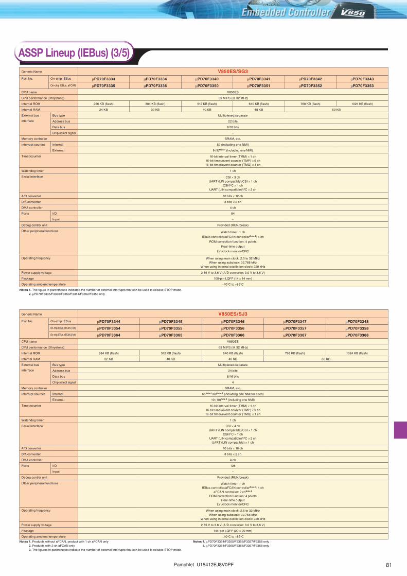
Pamphlet U15412EJ8V0PF �1
Generic Name V850ES/SG3Part No. On-chip IEBus mPD70F3333 mPD70F3334 mPD70F3340 mPD70F3341 mPD70F3342 mPD70F3343
On-chip IEBus, aFCAN mPD70F3335 mPD70F3336 mPD70F3350 mPD70F3351 mPD70F3352 mPD70F3353
CPU name V850ES
CPU performance (Dhrystone) 69 MIPS (@ 32 MHz)
Internal ROM 256 KB (flash) 384 KB (flash) 512 KB (flash) 640 KB (flash) 768 KB (flash) 1024 KB (flash)
Internal RAM 24 KB 32 KB 40 KB 48 KB 60 KB
External businterface
Bus type Multiplexed/separate
Address bus 22 bits
Data bus 8/16 bits
Chip select signal -
Memory controller SRAM, etc.
Interrupt sources Internal 52 (including one NMI)
External 9 (9)Note 1 (including one NMI)
Timer/counter 16-bit interval timer (TMM) × 1 ch16-bit timer/event counter (TMP) × 6 ch16-bit timer/event counter (TMQ) × 1 ch
Watchdog timer 1 ch
Serial interface CSI × 3 chUART (LIN compatible)/CSI × 1 ch
CSI/I2C × 1 chUART (LIN compatible)/I2C × 2 ch
A/D converter 10 bits × 12 ch
D/A converter 8 bits × 2 ch
DMA controller 4 ch
Ports I/O 84
Input -
Debug control unit Provided (RUN/break)
Other peripheral functions Watch timer: 1 chIEBus controller/aFCAN controllerNote 2: 1 ch
ROM correction function: 4 pointsReal-time output
LVI/clock monitor/CRC
Operating frequency When using main clock: 2.5 to 32 MHzWhen using subclock: 32.768 kHz
When using internal oscillation clock: 220 kHz
Power supply voltage 2.85 V to 3.6 V (A/D converter: 3.0 V to 3.6 V)
Package 100-pin LQFP (14 × 14 mm)
Operating ambient temperature -40°C to +85°CNotes 1. The figure in parentheses indicates the number of external interrupts that can be used to release STOP mode.
2. mPD70F3335/F3336/F3350/F3351/F3352/F3353 only
Generic Name V850ES/SJ3Part No. On-chip IEBus mPD70F3344 mPD70F3345 mPD70F3346 mPD70F3347 mPD70F3348
On-chip IEBus, aFCAN (1 ch) mPD70F3354 mPD70F3355 mPD70F3356 mPD70F3357 mPD70F3358
On-chip IEBus, aFCAN (2 ch) mPD70F3364 mPD70F3365 mPD70F3366 mPD70F3367 mPD70F3368
CPU name V850ES
CPU performance (Dhrystone) 69 MIPS (@ 32 MHz)
Internal ROM 384 KB (flash) 512 KB (flash) 640 KB (flash) 768 KB (flash) 1024 KB (flash)
Internal RAM 32 KB 40 KB 48 KB 60 KB
External businterface
Bus type Multiplexed/separate
Address bus 24 bits
Data bus 8/16 bits
Chip select signal 4
Memory controller SRAM, etc.
Interrupt sources Internal 65Note 1/69Note 2 (including one NMI for each)
External 10 (10)Note 3 (including one NMI)
Timer/counter 16-bit interval timer (TMM) × 1 ch16-bit timer/event counter (TMP) × 9 ch16-bit timer/event counter (TMQ) × 1 ch
Watchdog timer 1 ch
Serial interface CSI × 4 chUART (LIN compatible)/CSI × 1 ch
CSI/I2C × 1 chUART (LIN compatible)/I2C × 2 ch
UART (LIN compatible) × 1 ch
A/D converter 10 bits × 16 ch
D/A converter 8 bits × 2 ch
DMA controller 4 ch
Ports I/O 128
Input -
Debug control unit Provided (RUN/break)
Other peripheral functions Watch timer: 1 chIEBus controller/aFCAN controllerNote 4: 1 ch
aFCAN controller: 2 chNote 5
ROM correction function: 4 pointsReal-time output
LVI/clock monitor/CRC
Operating frequency When using main clock: 2.5 to 32 MHzWhen using subclock: 32.768 kHz
When using internal oscillation clock: 220 kHz
Power supply voltage 2.85 V to 3.6 V (A/D converter: 3.0 V to 3.6 V)
Package 144-pin LQFP (20 × 20 mm)
Operating ambient temperature -40°C to +85°CNotes 1. Products without aFCAN, product with 1 ch aFCAN only
2. Products with 2 ch aFCAN only3. The figures in parentheses indicate the number of external interrupts that can be used to release STOP mode.
Notes 4. mPD70F3354/F3355/F3356/F3357/F3358 only5. mPD70F3364/F3365/F3366/F3367/F3368 only
ASSP Lineup (IEBus) (3/5)

�� Pamphlet U15412EJ8V0PF
Generic Name V850E/SJ3-H (Under Development)Part No. On-chip IEBus mPD70F3474 mPD70F3477
On-chip IEBus/aFCAN (1 ch) mPD70F3475 mPD70F3478
On-chip IEBus/aFCAN (1 ch), aFCAN (1 ch) mPD70F3476 mPD70F3479
CPU name V850E1
CPU performance (Dhrystone) 95 MIPS (@ 48 MHz)
Internal ROM 1280 KB (flash) 1536 KB (flash)
Internal RAM 92 KB (internal RAM: 60 KB, expanded internal RAM: 32 KB)
External businterface
Bus type Multiplexed/separate
Address bus 24 bits
Data bus 8/16 bits
Chip select signal 4
Memory controller SRAM, etc.
Interrupt sources Internal 95Note 1/99Note 2/103Note 3 (including one NMI for each)
External 11 (11)Note 4 (including one NMI)
Timer/counter 16-bit interval timer (TMM) × 3 ch16-bit timer/event counter (TMP) × 9 ch (encoder count function: 2 ch)
16-bit timer/event counter (TMQ) × 1 ch
Watchdog timer 1 ch
Serial interface UART/CSI × 1 ch, UART/I2C × 2 ch, UART/CSI/I2C × 1 ch, UART/CSI (FIFO compatible) × 1 ch, CSI/I2C × 1 ch, UART × 1 ch, UART (FIFO compatible) × 2 ch, CSI × 3 ch, CSI (FIFO compatible) × 1 ch, I2C × 2 ch
orUART/CSI × 1 ch, UART/I2C × 1 ch, UART/CSI/I2C × 2 ch, UART/CSI (FIFO compatible) × 1 ch,
CSI/I2C × 1 ch, UART × 1 ch, UART (FIFO compatible) × 2 ch, CSI × 2 ch, CSI (FIFO compatible) × 1 ch, I2C × 2 ch
A/D converter 10 bits × 16 ch
D/A converter 8 bits × 2 ch
DMA controller 4 ch
Ports I/O 128
Input -
Debug control unit Provided (RUN/break)
Other peripheral functions Watch timer: 1 chReal-time counter (Watch timer): 1 ch
IEBus controller/aFCAN controllerNote 5: 1 chaFCAN controller: 2 chNote 6
ROM correction function: 8 pointsReal-time output
LVI/clock monitor/CRC, SSCG
Operating frequency When using main: 48 MHz (max.)When using subclock: 32.768 kHz
When using internal oscillation clock: 220 kHz
Power supply voltage 2.85 V to 3.6 V (A/D converter, D/A converter: 3.0 V to 3.6 V)
Package 144-pin LQFP (20 × 20 mm)
Operating ambient temperature -40°C to +85°C
Generic Name V850E/SK3-H (Under Development)Part No. On-chip IEBus mPD70F3480
On-chip IEBus, aFCAN (1 ch) mPD70F3481
On-chip IEBus, aFCAN (2 ch) mPD70F3482
CPU name V850E1
CPU performance (Dhrystone) 95 MIPS (@ 48 MHz)
Internal ROM 1536 KB (flash)
Internal RAM 92 KB (internal RAM: 60 KB, expanded internal RAM: 32 KB)
External businterface
Bus type Multiplexed/separate
Address bus 24 bits
Data bus 8/16 bits
Chip select signal 4
Memory controller SRAM, etc.
Interrupt sources Internal 95Note 1/99Note 2/103Note 3 (including one NMI for each)
External 11 (11)Note 4 (including one NMI)
Timer/counter 16-bit interval timer (TMM) × 3 ch16-bit timer/event counter (TMP) × 9 ch (encoder count function: 2 ch)
16-bit timer/event counter (TMQ) × 1 ch
Watchdog timer 1 ch
Serial interface UART/CSI × 1 ch, UART/I2C × 2 ch, UART/CSI/I2C × 1 ch, UART/CSI (FIFO compatible) × 1 ch, CSI/I2C × 1 ch, UART × 1 ch, UART (FIFO compatible) × 2 ch, CSI × 3 ch, CSI (FIFO compatible) × 1 ch, I2C × 2 ch
orUART/CSI × 1 ch, CSI/I2C × 2 ch, UART × 5 ch, UART (FIFO compatible) × 2 ch, CSI × 3 ch, CSI (FIFO compatible) × 2 ch, I2C × 4 ch
A/D converter 10 bits × 16 ch
D/A converter 8 bits × 2 ch
DMA controller 4 ch
Ports I/O 156
Input -
Debug control unit Provided (RUN/break)
Other peripheral functions Watch timer: 1 chReal-time counter (watch timer): 1 ch
IEBus controller/aFCAN controllerNote 5: 1 chaFCAN controller: 2 chNote 6
ROM correction function: 8 pointsReal-time output
LVI/clock monitor/CRC, SSCG
Operating frequency When using main clock: 48 MHz (max.)When using subclock: 32.768 kHz
When using internal oscillation clock: 220 kHz
Power supply voltage 2.85 V to 3.6 V (A/D converter, D/A converter: 3.0 V to 3.6 V)
Package 176-pin LQFP (24 × 24 mm)
Operating ambient temperature -40°C to +85°C
ASSP Lineup (IEBus) (4/5)
Notes 1. Products without aFCAN only2. Products with 1 ch aFCAN only3. Products with 2 ch aFCAN only
Notes 4. The figure in parentheses indicates the number of external interrupts that can be used to release STOP mode.5. mPD70F3475, 70F34786. mPD70F3476, 70F3479
Notes 1. Products without aFCAN only2. Products with 1 ch aFCAN only3. Products with 2 ch aFCAN only
Notes 4. The figure in parentheses indicates the number of external interrupts that can be used to release STOP mode.5. mPD70F34816. mPD70F3482

Pamphlet U15412EJ8V0PF ��
Generic Name V850ES/SG2-H V850ES/SG2Part No. mPD703272HY mPD703273HY mPD70F3273HY mPD703270Y mPD703271Y mPD70F3271Y mPD703272Y mPD703273Y mPD70F3273Y
CPU name V850ES V850ES
CPU performance (Dhrystone) 66 MIPS (@ 32 MHz) 43 MIPS (@ 20 MHz)
Internal ROM 512 KB (mask) 640 KB (mask) 640 KB (flash) 256 KB (mask) 384 KB (mask) 384 KB (flash) 512 KB (mask) 640 KB (mask) 640 KB (flash)
Internal RAM 40 KB 48 KB 24 KB 32 KB 40 KB 48 KB
External businterface
Bus type Multiplexed/separate Multiplexed/separate
Address bus 22 bits 22 bits
Data bus 8/16 bits 8/16 bits
Chip select signal - -
Memory controller SRAM, etc. SRAM, etc.
Interrupt sources Internal 51 (including one NMI) 52 (including one NMI)
External 9 (9)Note 1 (including one NMI) 9 (9)Note 1 (including one NMI)
Timer/counter 16-bit interval timer (TMM) × 1 ch16-bit timer/event counter (TMP) × 6 ch16-bit timer/event counter (TMQ) × 1 ch
16-bit interval timer (TMM) × 1 ch16-bit timer/event counter (TMP) × 6 ch16-bit timer/event counter (TMQ) × 1 ch
Watchdog timer 1 ch 1 ch
Serial interface CSI × 3 chUART (LIN compatible)/CSI × 1 ch
CSI/I2C × 1 chUART (LIN compatible)/I2C × 2 ch
CSI × 3 chUART (LIN compatible)/CSI × 1 ch
CSI/I2C × 1 chUART (LIN compatible)/I2C × 2 ch
A/D converter 10 bits × 12 ch 10 bits × 12 ch
D/A converter 8 bits × 2 ch 8 bits × 2 ch
DMA controller 4 ch 4 ch
Ports I/O 84 84
Input - -
Debug control unit - Provided (RUN/break) - Provided (RUN/break) - Provided (RUN/break)
Other peripheral functions Watch timer: 1 chIEBus controller: 1 ch
ROM correction function: 4 pointsReal-time output
Clock monitor/CRC
Watch timer: 1 chIEBus controller: 1 ch
ROM correction function: 4 pointsReal-time output
LVI/clock monitor/CRC
Operating frequency When using main clock: 2.5 to 32 MHzWhen using subclock: 32.768 kHz
When using internal oscillation clock: 200 kHz
When using main clock: 2.5 to 20 MHzWhen using subclock: 32.768 kHz
When using internal oscillation clock: 200 kHz
Power supply voltage 3.0 V to 3.6 V 2.85 V to 3.6 V (A/D converter: 3.0 V to 3.6 V)
Package 100-pin LQFP (14 × 14 mm) 100-pin LQFP (14 × 14 mm)100-pin QFP (14 × 20 mm)Note 2
Operating ambient temperature -40°C to +85°C -40°C to +85°C
Notes 1. The figure in parentheses indicates the number of external interrupts that can be used to release STOP mode.2. mPD703270Y/3271Y/F3271Y only
Generic Name V850ES/SJ2-H V850ES/SJ2Part No. mPD703275HY mPD703276HY mPD70F3276HY mPD703274Y mPD70F3274Y mPD703275Y mPD703276Y mPD70F3276Y
CPU name V850ES V850ES
CPU performance (Dhrystone) 66 MIPS (@ 32 MHz) 43 MIPS (@ 20 MHz)
Internal ROM 512 KB (mask) 640 KB (mask) 640 KB (flash) 384 KB (mask) 384 KB (flash) 512 KB (mask) 640 KB (mask) 640 KB (flash)
Internal RAM 40 KB 48 KB 32 KB 40 KB 48 KB
External businterface
Bus type Multiplexed/separate Multiplexed/separate
Address bus 24 bits 24 bits
Data bus 8/16 bits 8/16 bits
Chip select signal 4 4
Memory controller SRAM, etc. SRAM, etc.
Interrupt sources Internal 64 (including one NMI) 65 (including one NMI)
External 10 (10)Note (including one NMI) 10 (10)Note (including one NMI)
Timer/counter 16-bit interval timer (TMM) × 1 ch16-bit timer/event counter (TMP) × 9 ch16-bit timer/event counter (TMQ) × 1 ch
16-bit interval timer (TMM) × 1 ch16-bit timer/event counter (TMP) × 9 ch16-bit timer/event counter (TMQ) × 1 ch
Watchdog timer 1 ch 1 ch
Serial interface CSI × 4 chUART (LIN compatible)/CSI × 1 ch
CSI/I2C × 1 chUART (LIN compatible)/I2C × 2 ch
UART (LIN compatible) × 1 ch
CSI × 4 chUART (LIN compatible)/CSI × 1 ch
CSI/I2C × 1 chUART (LIN compatible)/I2C × 2 ch
UART (LIN compatible) × 1 ch
A/D converter 10 bits × 16 ch 10 bits × 16 ch
D/A converter 8 bits × 2 ch 8 bits × 2 ch
DMA controller 4 ch 4 ch
Ports I/O 128 128
Input - -
Debug control unit - Provided (RUN/break) - Provided (RUN/break) - Provided (RUN/break)
Other peripheral functions Watch timer: 1 chIEBus controller: 1 ch
ROM correction function: 4 pointsReal-time output
Clock monitor/CRC
Watch timer: 1 chIEBus controller: 1 ch
ROM correction function: 4 pointsReal-time output
LVI/clock monitor/CRC
Operating frequency When using main clock: 2.5 to 32 MHzWhen using subclock: 32.768 kHz
When using internal oscillation clock: 200 kHz
When using main clock: 2.5 to 20 MHzWhen using subclock: 32.768 kHz
When using internal oscillation clock: 200 kHz
Power supply voltage 3.0 V to 3.6 V 2.85 V to 3.6 V (A/D converter: 3.0 V to 3.6 V)
Package 144-pin LQFP (20 × 20 mm) 144-pin LQFP (20 × 20 mm)
Operating ambient temperature -40°C to +85°C -40°C to +85°C
Note The figure in parentheses indicates the number of external interrupts that can be used to release STOP mode.
ASSP Lineup (IEBus) (5/5)

V850 Development Environment
The V850 development environment
consists of tools designed to make the
development of application systems
using the high-performance
V850 microcontrollers made by
NEC Electronics more pleasant, faster,
and more accurate.
Each one of these development tools
features functions to fully exploit the
performance of the V850 microcontrollers.
Pamphlet U15412EJ8V0PF��
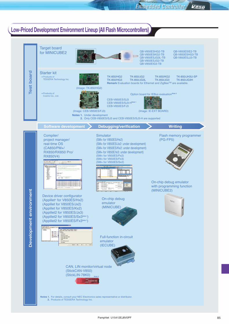
Pamphlet U15412EJ8V0PF ��
V850 Development Environment
The V850 development environment
consists of tools designed to make the
development of application systems
using the high-performance
V850 microcontrollers made by
NEC Electronics more pleasant, faster,
and more accurate.
Each one of these development tools
features functions to fully exploit the
performance of the V850 microcontrollers.
Software development Debugging/verification Writing
De
ve
lop
me
nt
envir
onm
ent
Compiler/project manager/real-time OS(CA850/PM+/RX850/RX850 Pro/RX850V4)
Device driver configurator (Applilet® for V850ES/Hx2)(Applilet for V850ES/Jx2)(Applilet for V850ES/Kx2)(Applilet2 for V850ES/Jx3)(Applilet2 for V850ES/Sx3Note 1)(Applilet2 for V850ES/Fx3Note 1)
Full-function in-circuit emulator(IECUBE)
CAN, LIN monitor/virtual node(StickCAN-V850)(StickLIN-78K0)
On-chip debug emulator
(MINICUBE)
Simulator (SM+ for V850ES/Hx2)(SM+ for V850ES/Jx2: under development)(SM+ for V850ES/Kx2: under development)(SM+ for V850E/Ix3: under development)(SM+ for V850ES/Fx2)(SM+ for V850ES/Fx3)(SM+ for V850ES/Sx2)
Flash memory programmer(PG-FP5)
On-chip debug emulator with programming function(MINICUBE2)
Notes 1. For details, consult your NEC Electronics sales representative or distributor.2. Products of TESSERA Technology Inc.
Target board for MINICUBE2
Starter kit
QB-V850ESHG2-TB QB-V850ESIE2-TBQB-V850ESKG2-TB QB-V850ESHG3-TBQB-V850ESJG3L-TB QB-V850ESJJ3-TBQB-V850ESJG2-TBQB-V850EIG3-TB
• Products ofTESSERA Technology Inc.
(Image: TK-850/HG2)
TK-850/HG2 TK-850/JG2 TK-850/KG2 TK-850/JH3U-SPTK-850/HG3 TK-850/JG3L TK-850/JG3 TK-850/JG3H Remark Evaluation boards for Ethernet and ZigBeeTM are available.
Notes 1. Under development2. Only CEB-V850ES/SJ3 and CEB-V850ES/SJ3-H are supported
• Products ofCosmo Co., Ltd.
(Image: CEB-V850ES/FJ3)
CEB-V850ES/SJ3CEB-V850ES/SJ3-HNote 1
CEB-V850ES/FJ3
(Image: IE-EXT BOARD)
Option board for IEBus evaluationNote 2
Note 2
Te
st
bo
ard
Low-Priced Development Environment Lineup (All Flash Microcontrollers)

�� Pamphlet U15412EJ8V0PF
Product planning
System design
System debugging
System evaluation
Commercialization
PM+
Hardware tools
Software tools
CA850
DF703xxx
SM850, SM+
ID850, ID850QB
+RD850, +RD850 Pro, +RD850V4+AZ850, +AZ850V4
Hardware design
Fabrication
Stand-alone testing
Software design
Coding
Compiling/assembly
Debugging
RX850, RX850 Pro,RX850V4
Applilet
IE, IECUBE,MINICUBE,MINICUBE2
Development Flow
Development Tools (1/2)
Software tools
Product NameSoftware package SP850C compiler CA850Note 1
Device file DF703xxxNote 2
Project Manager PM+Notes 1, 3
Integrated debugger ID850Note 1, ID850QBNote 4
System simulator SM850Note 1, SM+Note 5
Real-time OS RX850, RX850 Pro, RX850V4Task debuggerNote 6 RD850, RD850 Pro, RD850V4System performance analyzerNote 6 AZ850, AZ850V4Middleware AP703000-Bxxx, AP703100-BxxxDevice driver configurator Applilet
Notes 1. Packaged in SP8502. Download from the NEC Electronics website.
(URL: http://www.necel.com/micro/en/index.html)3. Included with CA8504. Included with IECUBE and MINICUBE.5. Instruction simulation version: Included with SP850.
Instruction + peripheral simulation version: Sold separately6. Included with RX850, RX850 Pro, and RX850V4
Remark For details, refer to the 78K, V850 Microcontrollers Development Environment Pamphlet (U18355E).

Pamphlet U15412EJ8V0PF ��
Development Tools (2/2)
Hardware tools (when using IECUBE)
Target DeviceNote1 On-Chip Debug EmulatorV850ES/HE2, V850ES/HF2, V850ES/HG2, V850ES/HJ2, V850ES/HE3, V850ES/HF3, V850ES/HG3, V850ES/HJ3,V850ES/IE2, V850ES/JF3-L, V850ES/JG2, V850ES/JG3, V850ES/JG3-L, V850ES/JG3-H, V850ES/JG3-U, V850ES/JH3-H,V850ES/JH3-U, V850E/SJ3-HNote 2, V850E/SK3-HNote 2, V850ES/JJ2, V850ES/JJ3, V850ES/KE2, V850ES/KF2, V850ES/KG2,V850ES/KJ2, V850E/IF3, V850E/IG3, V850ES/KE1+, V850ES/KF1+, V850ES/KG1+, V850ES/KJ1+, V850ES/FE2,V850ES/FF2, V850ES/FG2, V850ES/FJ2, V850ES/FE3, V850ES/FF3, V850ES/FG3, V850ES/FJ3, V850ES/FK3,V850ES/FE3-L,V850ES/FF3-L, V850ES/FG3-L, V850ES/SG2, V850ES/SG2-H, V850ES/SJ2, V850ES/SJ2-H,V850ES/SG3, V850ES/SJ3, V850E/IA3, V850E/IA4, V850ES/IK1, V850E/MA3V850ES/HE2, V850ES/HF2, V850ES/HG2, V850ES/HJ2, V850ES/HE3, V850ES/HF3, V850ES/HG3, V850ES/HJ3,V850ES/JF3-L, V850ES/JG2, V850ES/JG3, V850ES/JG3-L, V850ES/JG3-H, V850ES/JG3-U, V850ES/JH3-H,V850ES/JH3-U, V850E/SJ3-HNote 2, V850E/SK3-HNote 2, V850ES/JJ2, V850ES/JJ3, V850ES/KJ2, V850E/IG3,V850E/ME2, V850E/MA3, V850E/IA4, V850E/SV2, V850E2/ME3, V850ES/SG2, V850ES/SG2-H, V850ES/SG3,V850ES/SJ2, V850ES/SJ2-H, V850ES/SJ3, V850ES/KE1+Note 3, V850ES/KF1+Note 3, V850ES/KG1+Note 3, V850ES/KJ1+,V850ES/KE2Note 3, V850ES/KF2Note 3, V850ES/KG2Note 3, V850ES/KJ2, V850ES/FE2, V850ES/FF2, V850ES/FG2, V850ES/FJ2,V850ES/FE3, V850ES/FF3, V850ES/FG3, V850ES/FJ3, V850ES/FK3, V850ES/FE3-L, V850ES/FF3-L, V850ES/FG3-L
QB-MINI2(generic name: MINICUBE2)
QB-V850MINI(generic name: MINICUBE)
Notes 1. Current as of November 2008. New target devices will be subsequently added.Although only the V850 microcontrollers are listed as target devices for MINICUBE2, some of the 78K microcontrollers are also target devices.
2. To be supported3. A self-check board is required to use MINICUBE
Remarks 1. A target connection cable, a connector conversion board, a target connector, and a debugger are included.A power supply and a PC interface board are not required.
2. For details, refer to the 78K, V850 Microcontrollers Development Environment Pamphlet (U18355E).
Hardware tools (when using MINICUBE or MINICUBE2)
Notes 1. A separate socket and probe are required for connection to the target system.An optional PC interface board (IE-70000-PCI-IF-A or IE-70000-CD-IF-A) is also required.
2. A separate socket is required for connection to the target system.An optional PC interface board (IE-70000-PCI-IF-A or IE-70000-CD-IF-A) is also required.
3. Depending on the target device package, a separate socket and probe may be required.The following items are required.• PC interface board: IE-70000-PCI-IF-A or IE-70000-CD-IF-A• Power supply: IE-70000-MC-PS-B
Remark For details, refer to the 78K, V850 Microcontrollers Development Environment Pamphlet (U18355E).
Target Device In-Circuit EmulatorMain Unit
V850E/IA1V850E/IA2
V850E/MA1, V850E/MA2
V850ES/SA2, V850ES/SA3V850ES/SG1, V850ES/SG2, V850ES/SG2-H, V850ES/SJ2, V850ES/SJ2-H, V850ES/SG3, V850ES/SJ3
IE-V850ES-G1
IE-V850E-MC-A
IE-V850E-MC
IE-703102-MC
IE-703002-MC
V850ES/PM1V850ES/FE2, V850ES/FF2, V850ES/FG2, V850ES/FJ2V850ES/ST2V850E/SV2
V850E/MS1 (5 V), V850E/MS2 (5 V)V850E/MS1 (3.3 V)V850/SA1V850/SB1, V850/SB2V850/SC1, V850/SC2, V850/SC3V853
IE-703116-MC-EM1IE-703114-MC-EM1
IE-703107-MC-EM1Note 3
IE-703204-G1-EM1Note 1 IE-703288-G1-EM1Note 2
IE-703228-G1-EM1Note 2
IE-703239-G1-EM1Note 2
IE-703220-G1-EM1Note 2 IE-703166-MC-EM1
IE-703102-MC-EM1Note 3 IE-703102-MC-EM1-AIE-703017-MC-EM1Note 3
IE-703037-MC-EM1Note 3
IE-703089-MC-EM1IE-703003-MC-EM1
Emulation Board
Hardware tools (when using other emulators)
Target Device In-Circuit EmulatorV850ES/SG1, V850ES/SG2, V850ES/SG2-H, V850ES/SJ2, V850ES/SJ2-H, V850ES/JG2, V850ES/JJ2,V850ES/JJ3, V850ES/JG3, V850ES/JF3-L, V850ES/JG3-L, V850ES/SG3, V850ES/SJ3V850E/IA3, V850E/IA4, V850ES/IK1V850ES/KE1+, V850ES/KE2, V850ES/KF1+, V850ES/KF2, V850ES/KG1+, V850ES/KG2, V850ES/KJ1+, V850ES/KJ2V850ES/FE2, V850ES/FF2, V850ES/FG2, V850ES/FJ2, V850ES/HE2, V850ES/HF2, V850ES/HG2, V850ES/HJ2V850ES/IE2V850ES/FE3, V850ES/FF3, V850ES/FG3, V850ES/FJ3, V850ES/FK3, V850ES/HE3, V850ES/HF3,V850ES/HG3, V850ES/HJ3, V850ES/FE3-L, V850ES/FF3-L, V850ES/FG3-L V850E/MA3V850E/IF3, V850E/IG3V850ES/JG3-H, V850ES/JG3-U, V850ES/JH3-H, V850ES/JH3-UV850E/SJ3-HNote, V850E/SK3-HNote
QB-V850ESSX2-ZZZ
QB-V850EIA4-ZZZQB-V850ESKX1H-ZZZ
QB-V850ESFX2-ZZZ
QB-V850ESIX2-ZZZQB-V850ESFX3-ZZZ
QB-V850EMA3-ZZZQB-V850EIX3-ZZZQB-V850ESJX3H-ZZZQB-V850ESX3H-ZZZ
Note To be supportedRemarks 1. A separate socket is required for each emulator above.
2. A USB interface cable, a debugger, and a simple programmer are included.A PC interface board is not required.
Remarks 3. The following items are required common to all devices.Power supply: QB-COMMON-PW-xxxx: Destination country
JP (Japan), EA (United States of America), CN (China), HK (Hong Kong), KR (South Korea),SG (Singapore), TW (Taiwan)
The product for each destination country will only be shipped for orders received from that country.4. For details, refer to the 78K, V850 Microcontrollers Development Environment Pamphlet (U18355E).

�� Pamphlet U15412EJ8V0PF
Development environment using in-circuit emulator, on-chip debug emulator
V850 Development Environment (1/2)
RD850Note 1
RD850 ProNote 1
RD850V4Note 2
RX850 RX850 ProRX850V4
CA850
CCV850CCV850E
GHS
XCC-VXASS-V
GAIO
AZ850Note 1
AZ850V4Note 2
ID850
AZ850Note 1
AZ850V4Note 2
ID850QB
ZIPC850ID850 CATS
AZ850Note 1
AZ850V4Note 2
MULTIGHS
KMC
AZ850Note 1
PARTNER
AZ850Note 1
WATCHPOINTSophia Systems
GNUProRed Hat
exeGCCKMC
micro VIEW-Gmicro VIEW-PLUS
YDC
G1 SeriesMC Series
MINICUBE Series
RTE SeriesMidas Lab
advice SeriesYDC
PARTNER SeriesKMC
UniSTAC SeriesIECUBE
Sophia Systems
IECUBE Series
AZ850Note 1
NW-V850-32NDK
ND SeriesNDK
Code DebuggerBITRAN DN-850 Series
BITRAN
Notes 1. The RD850, RD850 Pro, and AZ850 can be used with ID850, ID850QB, MULTI, PARTNER, WATCHPOINT, and NW-V850-32.2. The RD850V4 and AZ850V4 can be used with ID850, ID850QB, and MULTI.
NDK: Naito Densei Machida Mfg. Co., Ltd.Red Hat: Red Hat CorporationSophia Systems: Sophia Systems Co., Ltd.YDC: Yokogawa Digital Computer CorporationUnmarked: NEC Electronics
ATI: Accelerated Technology, Inc.BITRAN: BITRAN CorporationCATS: Communication and Technology Systems Inc.GAIO: Gaio Technology Co., Ltd.GHS: Green Hills Software, Inc.KMC: Kyoto Microcomputer Corporation
Midas Lab: Midas Lab Co., Ltd.
Task debuggerReal-time OS Compiler
Integrated developmentenvironment
AnalyzerDebugger In-circuit emulator/
on-chip debug emulator
Nucleus PLUSATI

Pamphlet U15412EJ8V0PF ��
Development environment using ROM emulator, evaluation board
V850 Development Environment (2/2)
Note The RD850, RD850 Pro, RD850V4, AZ850, and AZ850V4 can be used with MULTI and PARTNER.
RD850Note
RD850 ProNote
RD850V4Note
RX850 RX850 ProRX850V4
TK SeriesTESSERA
Midas Lab
RTE Series
Task debuggerReal-time OS ROM emulatorCompiler
AnalyzerDebugger
Evaluation board
Low-cost evaluation board (limited functions)Evaluation board
CA850
KMC
exeGCC
GHS
CCV850CCV850E
AZ850Note
KMC
AZ850V4Note
PARTNER
Red Hat
GNUPro
ATI
Nucleus PLUS
PMC
T-KernelPMC
GNU
GAIO
XCC-VXASS-V
GAIO
XDEB-VSystemSimulator
SHI
MDX700
GHS
MULTI
AZ850Note
AZ850V4Note
Monitor version ID850
SG-703111-1 V850E/ME2
SG-703500-1 V850E2/ME3PMC
V850E/MA3µT-Engine/V850E-MA3
ATI: Accelerated Technology, Inc.Red Hat: Red Hat CorporationGAIO: Gaio Technology Co., Ltd.
GHS: Green Hills Software, Inc.TESSERA: TESSERA Technology Inc.SHI Sumitomo Heavy Industries Mechatoronics, LTD.
PMC: Personal Media Corporation
Unmarked: NEC ElectronicsKMC: Kyoto Microcomputer CorporationMidas Lab: Midas Lab Co., Ltd.

�0 Pamphlet U15412EJ8V0PF
Software package (SP850) C compiler (CA850)
Software Products
Integrated debuggers (ID850, ID850QB)
Real-time OSs (RX850, RX850 Pro, RX850V4)
System simulators (SM850, SM+) Project manager (PM+)
n Product configuration The SP850 software package consists of the following software development tools. • C compiler (CA850) • Project Manager (PM+) • Integrated debugger (ID850) • System simulator (SM850, SM+ for V850) • Device file (DF703xxx)
n Features • Complies with ANSI-C, a C language standard.• Supports libraries for embedded systems • Compact code size and faster execution speed can be realized
through powerful optimization • Utilities useful for embedded systems (ROMization processor, etc.) • Description of embedded systems in C language (specification of
memory allocation and I/O register access) is possible.
n Features • Same operability as debugger • Target-less evaluation prior to target completion possible • In addition to the operation of the CPU itself, target system operation
including on-chip peripheral unit and interrupt servicing can also be simulated.
• Pseudo-target system construction and I/O operation are possiblethrough external parts.
• Data generated by 0/1 logic and timing charts can be input to theprogram being simulated.
• Larger number of events than in-circuit emulator • Construction by user target system users is possible through user
open interface. • A peripheral I/O register status can be specified and when this status
occurs, the system can be made to output an interrupt at the desired timing or transfer data to memory (peripheral I/O register event & action function).
n Target devicesV853, V850/SA1, V850/SB1, V850/SB2, V850/SC1, V850/SC2, V850/SC3, V850E/MS1, V850E/MA1, V850E/MA2, V850E/IA1, V850E/IA2, V850E/IF3Note 1,2, V850E/IG3Note 1,2, V850ES/SA2, V850ES/SA3, V850ES/SG1Note 1,2, V850ES/SG2Note 1, V850ES/SG2-HNote 1,2, V850ES/SJ2Note 1, V850ES/SJ2-HNote 1,2, V850ES/SG3Note 1,2, V850ES/SJ3Note 1,2, V850ES/FE2Note 1, V850ES/FF2Note 1, V850ES/FG2Note 1, V850ES/FJ2Note 1, V850ES/FE3Note 1, V850ES/FF3Note 1, V850ES/FG3Note 1, V850ES/FJ3Note 1, V850ES/FK3Note 1, V850ES/FE3-LNote 1,V850ES/FF3-LNote 1, V850ES/FG3-LNote 1, V850ES/HE2Note 1, V850ES/HF2Note 1,V850ES/HG2Note 1, V850ES/HJ2Note 1, V850ES/IE2Note 1,2,V850ES/JG2Note 1,2, V850ES/JJ2Note 1,2,V850ES/JJ3Note 1,2, V850ES/KE2Note 1,2, V850ES/KF2Note 1,2, V850ES/KG2Note 1,2, V850ES/KJ2Note 1,2, V850ES/JG3-HNote 1,2, V850ES/JG3-UNote 1,2, V850ES/JH3-HNote 1,2, V850ES/JH3-UNote 1,2, V850E/SJ3-HNote 1,2, V850E/SK3-HNote 1,2
Notes 1. These products are supported only by SM+.2. Under development
n Features • Project management (management of target chip, source, and
environment during debugging is possible.) • Supports wizard function during project creation • Automation of series of operations consisting of edit, build, and debug• Integration of Help function
n Features • Comply with global standards (mITRON specifications). • Support power management function. • Enable embedding of required functions only (selection of system
calls to be used). • Support sophisticated task development through task debugger (RD). • Support application operation analysis through system performance
analyzer (AZ)
n Features • Supports object files • Debugging at source level • Debugging using target resources • Real-time execution on target • Event setting according to complex software operation • Online help function

Pamphlet U15412EJ8V0PF �1
Task debuggers (RD850, RD850 Pro, RD850V4)
n Product configuration • TCP/IP protocol stack • Applications • LAN control driver
n Features • RFC-compliant • Support of numerous socket interfaces/libraries • Support of applications as option products • Provided device driver • Support of NEC Electronics real-time OS (RX850 Pro)
n Target devices V850E products
TCP/IP software library (RX-NET) for V850E products
Device driver configurator (Applilet)System performance analyzers (AZ850, AZ850V4)
n Features • Detection of bugs through system timing errors • Detection of bugs due to simultaneous operation of complex tasks • Detection/analysis of real-time system execution performance • Operation linked to various debuggers• Included with real-time OS (RX850, RX850 Pro, RX850V4)
n Features • Device driver generation support function
GUI operation automatically generates programs (device drivers) for controlling microcontroller peripheral functions (such as timers and A/D). In addition to functions for initialize processing of each peripheral function, functions for manipulating peripheral functions are provided as application program interfaces (APIs).
• Wide-ranging compatibility from 8 to 32 bitsFrom the 78K0S/Kx1+ (low pin count microcontrollers) to the V850 microcontrollers, a wide range of product types are supported, with a focus on All Flash microcontrollers. Applilet APIs have specifications in common with all products. Accordingly, once a program is developed using an Applilet, only the device driver needs to be exchanged when porting to a different microcontroller, greatly saving labor for porting.
• Ideal for learning how to program microcontrollersIdeal for those using microcontrollers for the first time, because the programs generated by the Applilet are not binary codes, but source codes (C language or assembler).
n Features • Display detailed information on OS resources such as tasks. • Display source of referenced tasks. • Included with real-time OS (RX850, RX850 Pro, RX850V4)

�� Pamphlet U15412EJ8V0PF
Time
Actually tested
Board design/development
Software design/development
Circuit diagrams attached This board usable for comparison purposes
Bundle OS/middleware
Various peripheral devices aremounted, so debugging
can be started fromdevice-independent parts
Provide user-own coding block as asample according to this board
I want to measureCPU performance.
Is it possible to realizesuch a function?
First time I use this device, pleaseprovide sample circuits.
I would like to useOS/middleware.
H/W
S/W
I want to start software developmentprior to the board development.
Likely to be a long time untilOS/middleware are ready
Not working properly. Is thecause hardware or software?
Deb
ug
SolutionGear provides the best solution in all these cases.
Devic
e se
lectio
n
By deepening cooperation with partner companies and forming an array of tools combining NEC Electronics-made tools and partner-made tools, NEC Electronics offers development environments that support the diverse needs of users.
Cooperation with partners
OSEK/VDX specifications compliant OS (RX-OSEK850)
RISC microcontroller reference platform (SolutionGearTM)
• KernelCompliant with OSEK/VDX OS Ver. 2.2.3 specificationsSupports 4 conformance classes: BCC1, BCC2, ECC1, and ECC2.
• ConfiguratorConfigurator allowing easy system information creation provided as standard.Configuration files support formats compatible with OIL Ver. 2.5.
• Task debugger (RD-OSEK850)Task debugger effective for application debugging using RX-OSEK850 provided as standard
• System performance analyzer (AZ-OSEK850)System performance analyzer for the RX-OSEK850 provided as standard.
n Features
• General-purpose evaluation boards available as RISC microcontroller software development platform• Target CPU: V850E/ME2, V850E2/ME3• Industry standard PC-compatible interfaces including PCI, ISA, PCMCIA, E-IDE, Ethernet, Serial, Parallel, PS/2, and USB, provided• CPU independent motherboards and CPU boards used combined• Bundled real-time OS, middleware, and sample drivers• MULTI/PARTNER remote monitor version can be used• Reference design information provided
n Features

Pamphlet U15412EJ8V0PF ��
On-chip debug emulator with programming function (MINICUBE2) On-chip debug emulator (MINICUBE)
Hardware Products
n Features • On-chip debugging and flash programming
Includes a debugging function which enables detection of microcontroller programming bugs and a programming function for writing developed programs to microcontrollers. Debugging to mass production can be processed with one device.
• Low priceBeing about 1/3 of the price of the current model MINICUBE allows further reduction of initial expenses related to development and mass production.
• 8-bit to 32-bit compatibleOne MINICUBE2 can handle various microcontrollers having differing performances, from development to mass production, allowing cost reduction and shared use of mass production systems through appropriation of development environments.
• Support of single power supply flash memory productsSupport is planned for all single power supply flash memory products to be released from now on, so MINICUBE2 can continue to be used in the future, too.
• Compact and light, includes wrist strapMeasuring only 48 × 48 × 13.9 mm, the volume is about 1/4 that of the current model MINICUBE. Furthermore, its compactness and lightness saves space for development and mass production, and it is easy to carry.
n Target devicesSee p. 87, Development Tools: Hardware tools (when using MINICUBE or MINICUBE2).
n Features • Low price
Cost is about 1/20 that of conventional high-performance emulators.Includes the debugger ID850QB.
• Simple setupUSB (1.1 or 2.0) is used for communication with the host machine, so power supply is unnecessary.
• Enables writing to on-chip flash memoryEvaluation can be started quickly, even without flash memory programmer.
• Maintenance enhancedSelf-diagnosis function is available and problems smoothly overcome by using the included self-check board.
• Compact and lightPocketable size makes it easy to carry
n Target devicesSee p. 87, Development Tools: Hardware tools (when using MINICUBE or MINICUBE2).

�� Pamphlet U15412EJ8V0PF
IE-V850E-MC, IE-V850E-MC-A, IE-703102-MC, IE-703002-MC
In-circuit emulators
IECUBE IE-V850ES-G1
n Features • Low price
Priced at 1/4 to 1/3 of conventional high-performance emulators.The debugger ID850QB and simple programmer MINICUBE2 are included.
• Easy setupEmulation board and emulator unit, which were separate products, are unified.USB (1.1 or 2.0) used for communication with host machine
• Rich debugging functionsAchieves functions similar to high-performance emulators (coverage and external memory emulation functions are optional). Often used time measurement, real-time RAM monitoring, and other functions enhanced.
• Maintenance enhancedSelf-diagnosis function is available and problems smoothly overcome.
• Compact and lightBeing palm-sized makes it easy to carry
n Target devicesSee p. 87, Development Tools: Hardware tools (when using IECUBE).
n Features • Emulator functions are integrated in one dedicated chip,
achieving high equivalence with an actual device.• Includes rich debugging functions such as breaking, tracing,
coverage measurement, external memory emulation, and real-time RAM monitoring.
• Easy to connect to the target system, using the extension probe provided as standard
• Internal power supply and easy to carry package• Connectable to various types of personal computers
n Target devicesSee p. 87, Development Tools: Hardware tools (when using other emulators).
n Features • Emulator functions are integrated in one dedicated chip, achieving
high equivalence with an actual device.• Rich emulation functions• Achieves operation frequencies equivalent to devices.• Connectable to various types of personal computers
n Target devicesSee p. 87, Development Tools: Hardware tools (when using other emulators).

Product information & Document download
•Products are categorized according to bit count andapplication, enabling direct access to the productyou need.
•A variety of information can be accessed, includingproduct features, product lineups, documents andrelated information.
Design Support
•The Website provides a range of helpful informationfor designers, including sample programs andcharacteristics data.
•The extensive FAQ helps with troubleshooting andoffers useful design hints.
Information about V850 microcontrollers and V850 microcontrollerdevelopment environment can be viewed at the NEC ElectronicsMicrocomputer Website.
Technical Update
•Notices concerning product restrictions anddevelopment tool upgradesNote can be downloadedfrom here.Note Excluding some products.
Development Tools Download
•V850 microcontroller development tools can bedownloaded from this area. Customers who areregistered users can receive upgrade informationby email.
http://www.necel.com/micro/en/ods/index.html
V850 Website
Pamphlet U15412EJ8V0PF ��

�� Pamphlet U15412EJ8V0PF
MEMO
Pamphlet U15412EJ8V0PF ��
Applilet is a registered trademark of NEC Electronics Corporation in Japan, Germany, Hong Kong, the People's Republic of China, the Republic of Korea, the United Kingdom, and the United States of America.IECUBE is a registered trademark of NEC Electronics Corporation in Japan and Germany.MINICUBE is a registered trademark of NEC Electronics Corporation in Japan and Germany and a trademark in the United States of America.PFESiP is a registered trademark of NEC Electronics Corporation in Japan, Germany, and United Kingdom.EEPROM, IEBus, SolutionGear, and VR are trademarks of NEC Electronics Corporation.MascotCapsule is a trademark of HI Corporation in Japan.MIPS is a registered trademark of MIPS Technologies, Inc. in the United States.ZigBee is a registered trademark of ZigBee Alliance in several countries including the United States and Japan.Windows is a registered trademark or a trademark of Microsoft Corporation in the United States and/or other countries.JAVA and all trademarks and logos related to JAVA are either registered trademarks or trademarks of Sun Microsystems, Inc. in the United States and/or other countries.Ethernet is a trademark of Xerox Corporation.TRON is an abbreviation of The Real-time Operating system Nucleus.ITRON is an abbreviation of Industrial TRON.mITRON is an abbreviation of Micro Industrial TRON.TRON, ITRON, and mITRON do not refer to specific products or product groups.All other marks or trademarks in this document are the property of their respective holders.
The information in this document is current as of October, 2008. The information is subject to change without notice. For actual design-in, refer to the latest publications of NEC Electronics data sheets or data books, etc., for the most up-to-date specifications of NEC Electronics products. Not all products and/or types are available in every country. Please check with an NEC Electronics sales representative for availability and additional information.No part of this document may be copied or reproduced in any form or by any means without the prior written consent of NEC Electronics. NEC Electronics assumes no responsibility for any errors that may appear in this document.NEC Electronics does not assume any liability for infringement of patents, copyrights or other intellectual property rights of third parties by or arising from the use of NEC Electronics products listed in this document or any other liability arising from the use of such products. No license, express, implied or otherwise, is granted under any patents, copyrights or other intellectual property rights of NEC Electronics or others.Descriptions of circuits, software and other related information in this document are provided for illustrative purposes in semiconductor product operation and application examples. The incorporation of these circuits, software and information in the design of a customer's equipment shall be done under the full responsibility of the customer. NEC Electronics assumes no responsibility for any losses incurred by customers or third parties arising from the use of these circuits, software and information.While NEC Electronics endeavors to enhance the quality, reliability and safety of NEC Electronics products, customers agree and acknowledge that the possibility of defects thereof cannot be eliminated entirely. To minimize risks of damage to property or injury (including death) to persons arising from defects in NEC Electronics products, customers must incorporate sufficient safety measures in their design, such as redundancy, fire-containment and anti-failure features.NEC Electronics products are classified into the following three quality grades: "Standard", "Special" and "Specific". The "Specific" quality grade applies only to NEC Electronics products developed based on a customer-designated "quality assurance program" for a specific application. The recommended applications of an NEC Electronics product depend on its quality grade, as indicated below. Customers must check the quality grade of each NEC Electronics product before using it in a particular application.
The quality grade of NEC Electronics products is "Standard" unless otherwise expressly specified in NEC Electronics data sheets or data books, etc. If customers wish to use NEC Electronics products in applications not intended by NEC Electronics, they must contact an NEC Electronics sales representative in advance to determine NEC Electronics' willingness to support a given application.
(Note)
•
•
•
•
•
•
M8E 02. 11-1
(1)
(2)
"NEC Electronics" as used in this statement means NEC Electronics Corporation and also includes its majority-owned subsidiaries."NEC Electronics products" means any product developed or manufactured by or for NEC Electronics (as defined above).
Computers, office equipment, communications equipment, test and measurement equipment, audioand visual equipment, home electronic appliances, machine tools, personal electronic equipmentand industrial robots.Transportation equipment (automobiles, trains, ships, etc.), traffic control systems, anti-disastersystems, anti-crime systems, safety equipment and medical equipment (not specifically designedfor life support).Aircraft, aerospace equipment, submersible repeaters, nuclear reactor control systems, lifesupport systems and medical equipment for life support, etc.
"Standard":
"Special":
"Specific":

32-bit Microcontrollers
V850
See your creations come to lifethrough the unsurpassedperformance of V850 microcontrollers.
NEC Electronics Corporation1753, Shimonumabe, Nakahara-ku,Kawasaki, Kanagawa 211-8668, JapanTel: 044-435-5111http://www.necel.com/
[America]
NEC Electronics America, Inc.2880 Scott Blvd.Santa Clara, CA 95050-2554, U.S.A.Tel: 408-588-6000 800-366-9782http://www.am.necel.com/
[Asia & Oceania]
NEC Electronics (China) Co., Ltd7th Floor, Quantum Plaza, No. 27 ZhiChunLu HaidianDistrict, Beijing 100083, P.R.ChinaTel: 010-8235-1155http://www.cn.necel.com/
Shanghai BranchRoom 2509-2510, Bank of China Tower,200 Yincheng Road Central,Pudong New Area, Shanghai, P.R.China P.C:200120Tel:021-5888-5400http://www.cn.necel.com/
Shenzhen BranchUnit 01, 39/F, Excellence Times Square Building,No. 4068 Yi Tian Road, Futian District, Shenzhen,P.R.China P.C:518048Tel:0755-8282-9800http://www.cn.necel.com/
NEC Electronics Hong Kong Ltd.Unit 1601-1613, 16/F., Tower 2, Grand Century Place,193 Prince Edward Road West, Mongkok, Kowloon, Hong KongTel: 2886-9318http://www.hk.necel.com/
NEC Electronics Taiwan Ltd.7F, No. 363 Fu Shing North RoadTaipei, Taiwan, R. O. C.Tel: 02-8175-9600http://www.tw.necel.com/
NEC Electronics Singapore Pte. Ltd.238A Thomson Road, #12-08 Novena Square, Singapore 307684Tel: 6253-8311http://www.sg.necel.com/
NEC Electronics Korea Ltd.11F., Samik Laviedʼor Bldg., 720-2,Yeoksam-Dong, Kangnam-Ku,Seoul, 135-080, KoreaTel: 02-558-3737http://www.kr.necel.com/
For further information, please contact:
G0706
[Europe]
NEC Electronics (Europe) GmbHArcadiastrasse 1040472 Düsseldorf, GermanyTel: 0211-65030http://www.eu.necel.com/
Hanover OfficePodbielskistrasse 166 B30177 HannoverTel: 0 511 33 40 2-0Munich OfficeWerner-Eckert-Strasse 981829 MünchenTel: 0 89 92 10 03-0Stuttgart OfficeIndustriestrasse 370565 StuttgartTel: 0 711 99 01 0-0United Kingdom BranchCygnus House, Sunrise ParkwayLinford Wood, Milton KeynesMK14 6NP, U.K.Tel: 01908-691-133Succursale Française9, rue Paul Dautier, B.P. 5278142 Velizy-Villacoublay CédexFranceTel: 01-3067-5800Sucursal en EspañaJuan Esplandiu, 1528007 Madrid, SpainTel: 091-504-2787Tyskland FilialTäby CentrumEntrance S (7th floor)18322 Täby, SwedenTel: 08 638 72 00Filiale ItalianaVia Fabio Filzi, 25/A20124 Milano, ItalyTel: 02-667541Branch The NetherlandsSteijgerweg 65616 HS EindhovenThe NetherlandsTel: 040 265 40 10
Document No. U15412EJ8V0PF00 (8th edition)Date Published January 2009 N © NEC Electronics Corporation 2002, 2004 January 2009