3. what is microprocessor? (a/m - 17) - dce. what is microprocessor? (a/m - 17) an integrated...
TRANSCRIPT


3. What is microprocessor? (A/M - 17) An integrated circuit that contains all the functions of a central processing unit of a computer. 4. What are the five types of instructions set in 8085 microprocessor? (A/M - 17)
Control Logical Branching Arithmetic Data Transfer 5. What is the function of Accumulator?
An accumulator is a register for short-term, intermediate storage of arithmetic and logic data in a
computer's CPU (central processing unit). In modern computers, any register can function as an
accumulator. The most elementary use for an accumulator is adding a sequence of numbers.
6. List the advantages of microprocessor. An advantage of Microprocessors is that these are general purpose electronic processing devices which can be programmed to execute a number of tasks. These are used in personal computers as well as a number of other embedded products.
o A microprocessor with 3 GHz is capable of performing 3 billion tasks per second. o Microprocessor is that it can quickly move data between the various memory locations.
7. What are the flags available in 8085 microprocessor? 8085 has five flags - Sign flag, Zero flag, Auxiliary carry flag, Parity flag and the Carry flag. 8. What is the function of IO/M signal in the 8085? It is a status signal. It is used to differentiate between memory locations and I/O operations. When this signal is low (IO/M = 0) it denotes the memory related operations. 9. What do you meant by opcode and the operand? Opcode is an instruction that tells processor what to do with the variable or data written besides it. Operand is a variable that stores data(and data can be a memory address or any data that we want to process).
10. What is indexing? Pointing of referencing objects with sequential numbers. Data bytes are stored in memory locations and those data bytes are referred to by their memory
locations.
11. What are the four components of a programmable machine? A typical programmable machine can be represented with four components. Microprocessor Memory Input Output

12. Define - Bus
A group of lines used to transfer bits between the microprocessor and other components of the computer
system.
13. What are the types of bus?
The types of bus are,
Address bus
Data bus
Control bus.
14. What is meant by 16 – bit register of 8085 microprocessor?
The 8085 has two 16 – bit register.
The program counter - The program counter is used to sequence the execution of a program.
Stack pointer - The stack pointer is used as a memory pointer for the stack memory.
DHANALAKSHMI COLLEGE OF ENGINEERING
Department of mechanical engineering
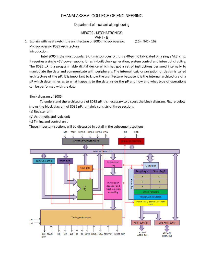
1. Explain with neat sketch the architecture of 8085 microprocessor. (16) (N/D - 16)
Microprocessor 8085 Architecture
Introduction
Intel 8085 is the most popular 8-bit microprocessor. It is a 40-pin IC fabricated on a single VLSI chip.
It requires a single +5V power supply. It has in-built clock generation, system control and interrupt circuitry.
The 8085 µP is a programmable digital device which has got a set of instructions designed internally to
manipulate the data and communicate with peripherals. The internal logic organization or design is called
architecture of the µP. It is important to know the architecture because it is the internal architecture of a
µP which determines as to what happens to the data inside the µP and how and what type of operations
can be performed with the data.
Block diagram of 8085
To understand the architecture of 8085 µP it is necessary to discuss the block diagram. Figure below
shows the block diagram of 8085 µP. It mainly consists of three sections
(a) Register unit
(b) Arithmetic and logic unit
(c) Timing and control unit
These important sections will be discussed in detail in the subsequent sections.
ME6702 - MECHATRONICS PART - B

Register unit
The microprocessor 8085 consists of different types of registers
(a) Accumulator
(b) General purpose registers
(c) Flag register
(d) Temporary register
(e) Program counter
(f) Stack pointer
Accumulator:
It is an 8-bit register which is used for performing all the arithmetic’s and logical operations.
Accumulator is also known as ‘register A’. During any mathematical or logical operation one of the
operands should be present in the accumulator. The final result is also stored in the accumulator.
General purpose registers:
Microprocessor 8085 architecture
There are six 8-bit general purpose registers B, C, D, E, H & L. General purpose registers are used for
temporary storage of data and intermediate results while the processor is executing the program. Two
eight bit registers can be combined for handling 16-bit data. Combination of two 8-bit registers is known as
pair. Valid register pairs are B-C, D-E, H-L. The H-L pair is used to address memories.
Flag register:
It is an 8-bit register in which five flip flops are used for checking condition. These flip flops are called flags.
Each of these flags can have the value either one or zero to indicate certain condition after arithmetic and
and logical operation. The five flags present in 8085 µP are:
(a) Sign flag (b) Zero flag (c) Auxiliary carry flag (d) Parity flag (e) Carry flag
Sign flag (S): After the execution of an arithmetic or logical operation, if bit D7 of the result is 1, the sign
flag is set. This flag is used with signed numbers and has no relevance for unsigned numbers. In a given
byte, if D7 is 1, the number is said to be negative and if it is 0, the number is considered as positive.
Zero Flag (Z): This flag is set if the result after arithmetic or logical operation turns out to be zero and is
reset if the result is non-zero.
Auxiliary carry (AC): This flag is set if in an arithmetic operation a carry is generated at bit D3 and passed
onto D4. This flag is used internally for BCD operations and is not available to the user unlike other flags. Parity (P): After an arithmetic or logical operation, if the result has an even number of 1s, the flag is set and
if there is odd number of 1s the flag is reset.
Carry (CY): If an arithmetic operation results in a carry, the flag is set otherwise it is reset. It also serves as a
borrow flag for subtraction.
The bit position reserved for these flags in the flag register are as follows:
Temporary register:-
Register W and Z are known as temporary registers. They are used by the µP for storing the data
temporarily during execution of a program. They are 8-bit registers and are not accessible to the user.

Program Counter:
It is a 16-bit register which holds the address of the instructions. Initially it indicates towards the starting
address of the program but after the first instruction is fetched the program counter automatically gets
incremented by one and points towards the next instruction. This process continues till the end of the
program.
Stack pointer:
The stack pointer is a 16-bit register which basically serves two purposes
(a) Points towards the stack memory. Initially it indicates the beginning of the stack memory. Whenever
something is added to the stack, the stack pointer is decremented and whenever something is removed
from the stack the stack pointer is incremented. Hence the stack pointer always points to the top of the
stack.
(b) Stack pointer also points towards the memory location where the µP has to go after attending an
interrupt or a subroutine; therefore it acts as a bookmark.
Arithmetic and logic unit:
This is the unit where all the arithmetic operations like addition, subtraction, multiplication and division
and logical operations like AND, OR, Ex-OR, complement, compare etc. are performed. It includes the
accumulator, the temporary register, the arithmetic and logic circuits and five flags. The temporary
registers are used to store data temporarily during an arithmetic/logical operation. The result is stored in
the accumulator and the flags are set or reset according to the result of the operation.
Timing and control unit:
The timing and control unit generates timing and control signals which are necessary for the execution of
instruction. It controls data flow between CPU and peripherals. It provides status, control and timing signals
which are required for the operation of memory and I/O devices.
8085 System Bus
System bus is basically a group of communication lines/wires that are responsible for transferring
information between different units of the device or peripherals. A typical microprocessor communicates
with memory and other devices using three buses: address bus, data bus and control bus.
Address bus: Address bus is a unidirectional group of 16 lines i.e. bits flow in one direction from the µP to
the peripheral devices. The 8085 µP with it’s 16 address lines is capable of addressing 216 =65536 (64K)
memory locations.
Data bus: Data bus carries data in binary form, between microprocessor and peripheral devices as well as
memory. It is a group of 8-bits and is bidirectional. Data bus also carries instructions from memory to the
microprocessor. Size of the bus therefore limits the number of possible instructions. The 8085 µP has 246
bit patterns amounting to 74 different instructions. These 74 different instructions are therefore called its
instruction set.
Control bus: The control bus is combination of various single lines that carry control signals. The control
lines are not group of lines like address and data bus but are individual lines. Microprocessor generates
specific control signals for every operation it performs.
The bus system of 8085 is shown in figure 3.2.
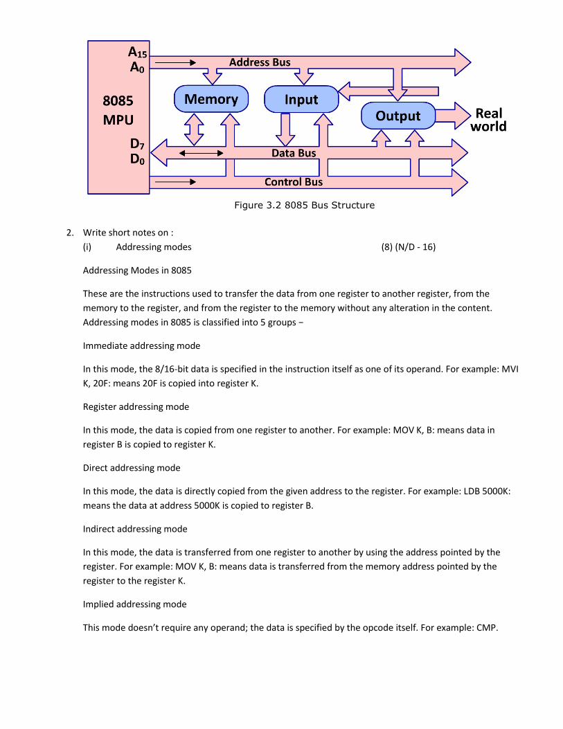
Figure 3.2 8085 Bus Structure
2. Write short notes on :
(i) Addressing modes (8) (N/D - 16)
Addressing Modes in 8085
These are the instructions used to transfer the data from one register to another register, from the
memory to the register, and from the register to the memory without any alteration in the content.
Addressing modes in 8085 is classified into 5 groups −
Immediate addressing mode
In this mode, the 8/16-bit data is specified in the instruction itself as one of its operand. For example: MVI
K, 20F: means 20F is copied into register K.
Register addressing mode
In this mode, the data is copied from one register to another. For example: MOV K, B: means data in
register B is copied to register K.
Direct addressing mode
In this mode, the data is directly copied from the given address to the register. For example: LDB 5000K:
means the data at address 5000K is copied to register B.
Indirect addressing mode
In this mode, the data is transferred from one register to another by using the address pointed by the
register. For example: MOV K, B: means data is transferred from the memory address pointed by the
register to the register K.
Implied addressing mode
This mode doesn’t require any operand; the data is specified by the opcode itself. For example: CMP.

(ii) Instruction set of 8085 microprocessor (8) (N/D - 16)
Instruction sets are instruction codes to perform some task. It is classified into five categories.
S.No
.
Instruction & Description
1
Control Instructions
Following is the table showing the list of Control instructions with their meanings.
Opcode Operand Meaning Explanation
NOP None No operation No operation is performed, i.e., the
instruction is fetched and decoded.
HLT None
Halt and
enter wait state
The CPU finishes executing the current
instruction and stops further execution. An interrupt or reset is necessary to exit from
the halt state.
DI None Disable interrupts
The interrupt enable flip-flop is reset and all the interrupts are disabled except TRAP.
2
Logical Instructions
Following is the table showing the list of Logical instructions with their meanings.
Opcode Operand Meaning Explanation
CMP R
M
Compare the register or memory with the
accumulator
The contents of the operand (register or memory) are M compared with the contents of the
accumulator.
CPI 8-bit data Compare immediate
with the accumulator
The second byte data is compared with the contents of the accumulator.
3 Branching Instructions
Following is the table showing the list of Branching instructions with their

meanings.
Opcode Operand Meaning Explanation
JMP 16-bit address Jump
unconditionally
The program
sequence is
transferred to the
memory address
given in the
operand.
Opcode Description Flag
Status
JC Jump on
Carry CY=1
JNC Jump on no
Carry CY=0
JP Jump on
positive S=0
JPO Jump on
parity odd P=0
16-bit address Jump
conditionally
The program
sequence is
transferred to the
memory address
given in the
operand based on
the specified flag
of the PSW.
4
Arithmetic Instructions
Following is the table showing the list of Arithmetic instructions with their
meanings.
Opcode Operand Meaning Explanation
ADD
R
M
Add register or
memory, to the
accumulator
The contents of the register
or memory are added to the
contents of the accumulator
and the result is stored in
the accumulator.

Example − ADD K.
5
Data Transfer Instructions
Following is the table showing the list of Data-transfer instructions with their
meanings.
Opcode Operand Meaning Explanation
MOV
Rd, Sc
M, Sc
Dt, M
Copy from the
source (Sc) to the
destination(Dt)
This instruction copies
the contents of the
source register into the
destination register
without any alteration.
Example − MOV K, L
MVI
Rd, data
M, data
Move immediate 8-
bit
The 8-bit data is stored
in the destination
register or memory.
Example − MVI K, 55L

3. Explain the pin diagram of 8085 Microprocessor. The following image depicts the pin diagram of 8085 Microprocessor −
The pins of a 8085 microprocessor can be classified into seven groups − Address bus A15-A8, it carries the most significant 8-bits of memory/IO address. Data bus AD7-AD0, it carries the least significant 8-bit address and data bus. Control and status signals These signals are used to identify the nature of operation. There are 3 control signal and 3 status signals. Three control signals are RD, WR & ALE.
RD − This signal indicates that the selected IO or memory device is to be read and is ready for accepting data available on the data bus.
WR − This signal indicates that the data on the data bus is to be written into a selected memory or IO location.
ALE − It is a positive going pulse generated when a new operation is started by the microprocessor. When the pulse goes high, it indicates address. When the pulse goes down it indicates data.
Three status signals are IO/M, S0 & S1. IO/M This signal is used to differentiate between IO and Memory operations, i.e. when it is high indicates IO operation and when it is low then it indicates memory operation.
S1 & S0 These signals are used to identify the type of current operation. Power supply There are 2 power supply signals − VCC & VSS. VCC indicates +5v power supply and VSS indicates ground signal. Clock signals There are 3 clock signals, i.e. X1, X2, CLK OUT.
X1, X2 − A crystal (RC, LC N/W) is connected at these two pins and is used to set frequency of the internal clock generator. This frequency is internally divided by 2.
CLK OUT − this signal is used as the system clock for devices connected with the microprocessor. Interrupts & externally initiated signals Interrupts are the signals generated by external devices to request the microprocessor to perform a task. There are 5 interrupt signals, i.e. TRAP, RST 7.5, RST 6.5, RST 5.5, and INTR. We will discuss interrupts in detail in interrupts section.
INTA − It is an interrupt acknowledgment signal. RESET IN − this signal is used to reset the microprocessor by setting the program counter to zero. RESET OUT − this signal is used to reset all the connected devices when the microprocessor is
reset. READY − this signal indicates that the device is ready to send or receive data. If READY is low,
then the CPU has to wait for READY to go high. HOLD − this signal indicates that another master is requesting the use of the address and data
buses. HLDA (HOLD Acknowledge) − It indicates that the CPU has received the HOLD request and it will
relinquish the bus in the next clock cycle. HLDA is set to low after the HOLD signal is removed. Serial I/O signals There are 2 serial signals, i.e. SID and SOD and these signals are used for serial communication.
SOD (Serial output data line) − the output SOD is set/reset as specified by the SIM instruction. SID (Serial input data line) − the data on this line is loaded into accumulator whenever a RIM
instruction is executed.
4. Mention the difference between the Microprocessor and Microcontrollers.
Microprocessor Micro Controller
Microprocessor is heart of Computer system. Micro Controller is a heart of embedded system.
It is just a processor. Memory and I/O components have to be connected externally
Micro controller has external processor along with internal memory and i/O components

Since memory and I/O has to be connected externally, the circuit becomes large.
Since memory and I/O are present internally, the circuit is small.
Cannot be used in compact systems and hence inefficient
Can be used in compact systems and hence it is an efficient technique
Cost of the entire system increases Cost of the entire system is low
Due to external components, the entire power consumption is high. Hence it is not suitable to used with devices running on stored power like batteries.
Since external components are low, total power consumption is less and can be used with devices running on stored power like batteries.
Most of the microprocessors do not have power saving features.
Most of the micro controllers have power saving modes like idle mode and power saving mode. This helps to reduce power consumption even further.
Since memory and I/O components are all external, each instruction will need external operation, hence it is relatively slower.
Since components are internal, most of the operations are internal instruction, hence speed is fast.
Microprocessor have less number of registers, hence more operations are memory based.
Micro controller have more number of registers, hence the programs are easier to write.
Microprocessors are based on von Neumann model/architecture where program and data are stored in same memory module
Micro controllers are based on Harvard architecture where program memory and Data memory are separate
Mainly used in personal computers Used mainly in washing machine, MP3 players
5. Explain the timing diagram of memory read and memory write cycle in 8085 microprocessor.
It is one of the best ways to understand to process of micro-processor/controller. With the help of timing
diagram we can understand the working of any system, step by step working of each instruction and its
execution, etc.
It is the graphical representation of process in steps with respect to time. The timing diagram represents the
clock cycle and duration, delay, content of address bus and data bus, type of operation ie.
Read/write/status signals.
Important terms related to timing diagrams:
1. Instruction cycle: this term is defined as the number of steps required by the cpu to complete the entire
process i.e. fetching and execution of one instruction. The fetch and execute cycles are carried out in
synchronization with the clock.
2. Machine cycle: It is the time required by the microprocessor to complete the operation of accessing the
memory devices or I/O devices. In machine cycle various operations like opcode fetch, memory read,
memory write, I/O read, I/O write are performed.
3. T-state: Each clock cycle is called as T-states.

Rules to identify number of machine cycles in an instruction:
1. If an addressing mode is direct, immediate or implicit then No. of machine cycles = No. of bytes.
2. If the addressing mode is indirect then No. of machine cycles = No. of bytes + 1. Add +1 to the No. of
machine cycles if it is memory read/write operation.
3. If the operand is 8-bit or 16-bit address then, No. of machine cycles = No. of bytes +1.
4. These rules are applicable to 80% of the instructions of 8085.
Timing Diagram:
Where, Instruction cycle= Fetch Cycle(FC) + Executecycle(EC).
Opcode fetch:
the microprocessor requires instructions to perform any particular action. In order to perform these actions
microprocessor utilizes Opcode which is a part of an instruction which provides detail (i.e. which operation
µp needs to perform) to microprocessor.

Fig:
Opcode fetch timing diagram
Operation:
During T1 state, microprocessor uses IO/M(bar), S0, S1 signals are used to instruct microprocessor to
fetch opcode.
Thus when IO/M(bar)=0, S0=S1= 1, it indicates opcode fetch operation.
During this operation 8085 transmits 16-bit address and also uses ALE signal for address latching.
At T2 state microprocessor uses read signal and make data ready from that memory location to read
opcode from memory and at the same time program counter increments by 1 and points next instruction to
be fetched.
In this state microprocessor also checks READY input signal, if this pin is at low logic level ie. '0' then
microprocessor adds wait state immediately between T2 and T3.
At T3, microprocessor reads opcode and store it into instruction register to decode it further.
During T4 microprocessor performs internal operation like decoding opcode and providing necessary
actions.
The opcode is decoded to know whether T5 or T6 states are required, if they are not required then µp
performs next operation.

3. Explain the pin diagram of 8085 Microprocessor. The following image depicts the pin diagram of 8085 Microprocessor −
The pins of a 8085 microprocessor can be classified into seven groups − Address bus A15-A8, it carries the most significant 8-bits of memory/IO address. Data bus AD7-AD0, it carries the least significant 8-bit address and data bus. Control and status signals These signals are used to identify the nature of operation. There are 3 control signal and 3 status signals. Three control signals are RD, WR & ALE.
RD − This signal indicates that the selected IO or memory device is to be read and is ready for accepting data available on the data bus.
WR − This signal indicates that the data on the data bus is to be written into a selected memory or IO location.
ALE − It is a positive going pulse generated when a new operation is started by the microprocessor. When the pulse goes high, it indicates address. When the pulse goes down it indicates data.
Three status signals are IO/M, S0 & S1. IO/M This signal is used to differentiate between IO and Memory operations, i.e. when it is high indicates IO operation and when it is low then it indicates memory operation.

S1 & S0 These signals are used to identify the type of current operation. Power supply There are 2 power supply signals − VCC & VSS. VCC indicates +5v power supply and VSS indicates ground signal. Clock signals There are 3 clock signals, i.e. X1, X2, CLK OUT.
X1, X2 − A crystal (RC, LC N/W) is connected at these two pins and is used to set frequency of the internal clock generator. This frequency is internally divided by 2.
CLK OUT − this signal is used as the system clock for devices connected with the microprocessor. Interrupts & externally initiated signals Interrupts are the signals generated by external devices to request the microprocessor to perform a task. There are 5 interrupt signals, i.e. TRAP, RST 7.5, RST 6.5, RST 5.5, and INTR. We will discuss interrupts in detail in interrupts section.
INTA − It is an interrupt acknowledgment signal. RESET IN − this signal is used to reset the microprocessor by setting the program counter to zero. RESET OUT − this signal is used to reset all the connected devices when the microprocessor is
reset. READY − this signal indicates that the device is ready to send or receive data. If READY is low,
then the CPU has to wait for READY to go high. HOLD − this signal indicates that another master is requesting the use of the address and data
buses. HLDA (HOLD Acknowledge) − It indicates that the CPU has received the HOLD request and it will
relinquish the bus in the next clock cycle. HLDA is set to low after the HOLD signal is removed. Serial I/O signals There are 2 serial signals, i.e. SID and SOD and these signals are used for serial communication.
SOD (Serial output data line) − the output SOD is set/reset as specified by the SIM instruction. SID (Serial input data line) − the data on this line is loaded into accumulator whenever a RIM
instruction is executed.
4. Mention the difference between the Microprocessor and Microcontrollers.
Microprocessor Micro Controller
Microprocessor is heart of Computer system. Micro Controller is a heart of embedded system.
It is just a processor. Memory and I/O components have to be connected externally
Micro controller has external processor along with internal memory and i/O components

Since memory and I/O has to be connected externally, the circuit becomes large.
Since memory and I/O are present internally, the circuit is small.
Cannot be used in compact systems and hence inefficient
Can be used in compact systems and hence it is an efficient technique
Cost of the entire system increases Cost of the entire system is low
Due to external components, the entire power consumption is high. Hence it is not suitable to used with devices running on stored power like batteries.
Since external components are low, total power consumption is less and can be used with devices running on stored power like batteries.
Most of the microprocessors do not have power saving features.
Most of the micro controllers have power saving modes like idle mode and power saving mode. This helps to reduce power consumption even further.
Since memory and I/O components are all external, each instruction will need external operation, hence it is relatively slower.
Since components are internal, most of the operations are internal instruction, hence speed is fast.
Microprocessor have less number of registers, hence more operations are memory based.
Micro controller have more number of registers, hence the programs are easier to write.
Microprocessors are based on von Neumann model/architecture where program and data are stored in same memory module
Micro controllers are based on Harvard architecture where program memory and Data memory are separate
Mainly used in personal computers Used mainly in washing machine, MP3 players
5. Explain the timing diagram of memory read and memory write cycle in 8085 microprocessor.
It is one of the best ways to understand to process of micro-processor/controller. With the help of timing
diagram we can understand the working of any system, step by step working of each instruction and its
execution, etc.
It is the graphical representation of process in steps with respect to time. The timing diagram represents the
clock cycle and duration, delay, content of address bus and data bus, type of operation ie.
Read/write/status signals.
Important terms related to timing diagrams:
1. Instruction cycle: this term is defined as the number of steps required by the cpu to complete the entire
process i.e. fetching and execution of one instruction. The fetch and execute cycles are carried out in
synchronization with the clock.
2. Machine cycle: It is the time required by the microprocessor to complete the operation of accessing the
memory devices or I/O devices. In machine cycle various operations like opcode fetch, memory read,
memory write, I/O read, I/O write are performed.
3. T-state: Each clock cycle is called as T-states.

Rules to identify number of machine cycles in an instruction:
1. If an addressing mode is direct, immediate or implicit then No. of machine cycles = No. of bytes.
2. If the addressing mode is indirect then No. of machine cycles = No. of bytes + 1. Add +1 to the No. of
machine cycles if it is memory read/write operation.
3. If the operand is 8-bit or 16-bit address then, No. of machine cycles = No. of bytes +1.
4. These rules are applicable to 80% of the instructions of 8085.
Timing Diagram:
Where, Instruction cycle= Fetch Cycle(FC) + Executecycle(EC).
Opcode fetch:
the microprocessor requires instructions to perform any particular action. In order to perform these actions
microprocessor utilizes Opcode which is a part of an instruction which provides detail (i.e. which operation
µp needs to perform) to microprocessor.

Fig:
Opcode fetch timing diagram
Operation:
During T1 state, microprocessor uses IO/M(bar), S0, S1 signals are used to instruct microprocessor to
fetch opcode.
Thus when IO/M(bar)=0, S0=S1= 1, it indicates opcode fetch operation.
During this operation 8085 transmits 16-bit address and also uses ALE signal for address latching.
At T2 state microprocessor uses read signal and make data ready from that memory location to read
opcode from memory and at the same time program counter increments by 1 and points next instruction to
be fetched.
In this state microprocessor also checks READY input signal, if this pin is at low logic level ie. '0' then
microprocessor adds wait state immediately between T2 and T3.
At T3, microprocessor reads opcode and store it into instruction register to decode it further.
During T4 microprocessor performs internal operation like decoding opcode and providing necessary
actions.
The opcode is decoded to know whether T5 or T6 states are required, if they are not required then µp
performs next operation.

6. Explain the control instructions.
Following is the table showing the list of Control instructions with their meanings.
Opcode Operand Meaning Explanation
NOP None No operation No operation is performed, i.e., the instruction is
fetched and decoded.
HLT None
Halt and
enter wait
state
The CPU finishes executing the current instruction
and stops further execution. An interrupt or reset is
necessary to exit from the halt state.
DI None Disable
interrupts
The interrupt enable flip-flop is reset and all the
interrupts are disabled except TRAP.
EI None Enable
interrupts
The interrupt enable flip-flop is set and all the
interrupts are enabled.
RIM None
Read
interrupt
mask
This instruction is used to read the status of
interrupts 7.5, 6.5, 5.5 and read serial data input bit.
SIM None Set interrupt
mask
This instruction is used to implement the interrupts
7.5, 6.5, 5.5, and serial data output.
7. Explain logical instructions
The following table shows the list of Logical instructions with their meanings.
Opcode Operand Meaning Explanation
CMP R
M
Compare the
register or
memory with the
accumulator
The contents of the operand (register or
memory) are M compared with the contents
of the accumulator.

CPI 8-bit data
Compare
immediate with the
accumulator
The second byte data is compared with the
contents of the accumulator.
ANA R
M
Logical AND
register or
memory with the
accumulator
The contents of the accumulator are logically
AND with M the contents of the register or
memory, and the result is placed in the
accumulator.
ANI 8-bit data
Logical AND
immediate with the
accumulator
The contents of the accumulator are logically
AND with the 8-bit data and the result is
placed in the accumulator.
XRA R
M
Exclusive OR
register or
memory with the
accumulator
The contents of the accumulator are
Exclusive OR with M the contents of the
register or memory, and the result is placed
in the accumulator.
XRI 8-bit data
Exclusive OR
immediate with the
accumulator
The contents of the accumulator are
Exclusive OR with the 8-bit data and the
result is placed in the accumulator.
ORA R
M
Logical OR
register or
memory with the
accumulator
The contents of the accumulator are logically
OR with M the contents of the register or
memory, and result is placed in the
accumulator.
ORI 8-bit data
Logical OR
immediate with the
accumulator
The contents of the accumulator are logically
OR with the 8-bit data and the result is
placed in the accumulator.
RLC None Rotate the
accumulator left
Each binary bit of the accumulator is rotated
left by one position. Bit D7 is placed in the
position of D0 as well as in the Carry flag.
CY is modified according to bit D7.
RRC None Rotate the
accumulator right
Each binary bit of the accumulator is rotated
right by one position. Bit D0 is placed in the
position of D7 as well as in the Carry flag.
CY is modified according to bit D0.
RAL None
Rotate the
accumulator left
through carry
Each binary bit of the accumulator is rotated
left by one position through the Carry flag. Bit
D7 is placed in the Carry flag, and the Carry
flag is placed in the least significant position
D0. CY is modified according to bit D7.
RAR None
Rotate the
accumulator right
through carry
Each binary bit of the accumulator is rotated
right by one position through the Carry flag.
Bit D0 is placed in the Carry flag, and the
Carry flag is placed in the most significant
position D7. CY is modified according to bit
D0.
CMA None Complement
accumulator
The contents of the accumulator are
complemented. No flags are affected.
CMC None Complement carry The Carry flag is complemented. No other
flags are affected.
STC None Set Carry Set Carry
8. Explain branching instructions.
The following table shows the list of Branching instructions with their meanings.
Opcode Operand Meaning Explanation
JMP 16-bit
address Jump unconditionally
The program sequence is
transferred to the memory address given in the operand.

Opcode Description Flag
Status
JC Jump on
Carry CY=1
JNC Jump on
no Carry CY=0
JP Jump on
positive S=0
JM Jump on
minus S=1
JZ Jump on
zero Z=1
JNZ Jump on
no zero Z=0
JPE Jump on
parity even P=1
JPO Jump on
parity odd P=0
16-bit address
Jump conditionally
The program sequence is transferred to the memory address given in the operand based on the specified flag of the PSW.
Opcode Description Flag
Status
CC Call on
Carry CY=1
CNC Call on no CY=0
16-bit address
Unconditional subroutine call
The program sequence is transferred to the memory address given in the operand. Before transferring, the address of the next instruction after CALL is pushed onto
the stack.
Carry
CP Call on
positive S=0
CM Call on
minus S=1
CZ Call on
zero Z=1
CNZ Call on no
zero Z=0
CPE Call on
parity even P=1
CPO Call on
parity odd P=0
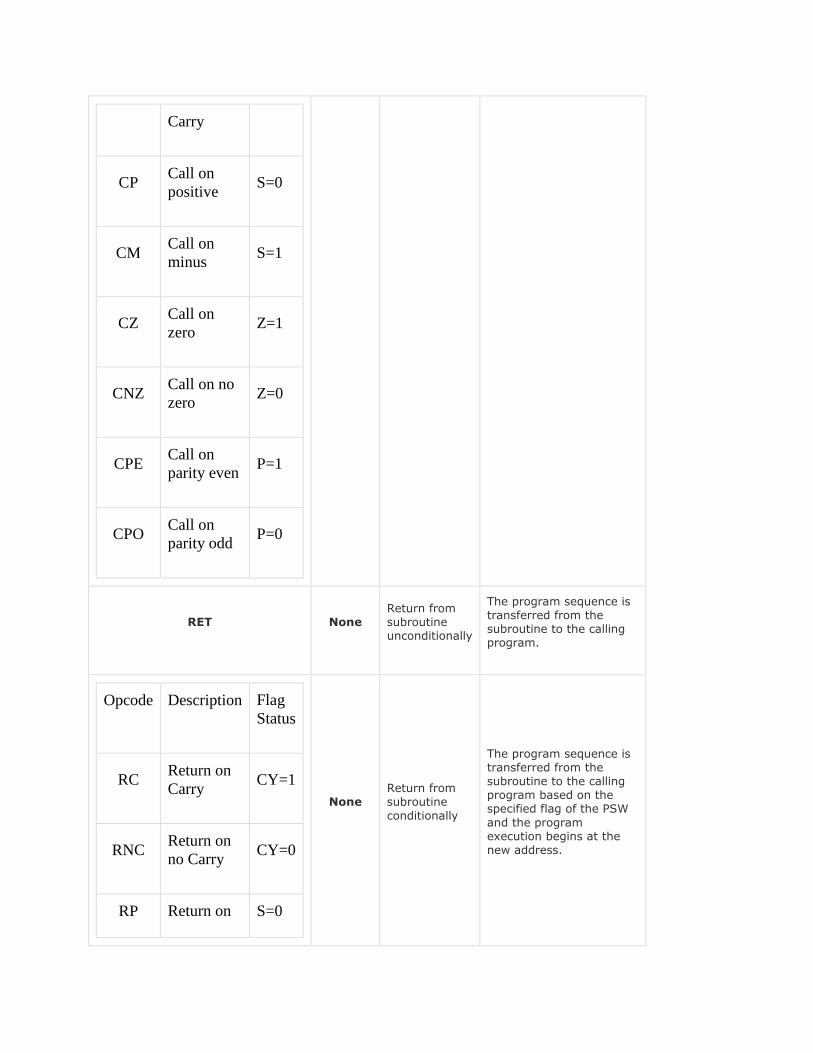
RET None Return from subroutine unconditionally
The program sequence is transferred from the subroutine to the calling program.
Opcode Description Flag
Status
RC Return on
Carry CY=1
RNC Return on
no Carry CY=0
RP Return on S=0
None Return from subroutine
conditionally
The program sequence is transferred from the subroutine to the calling program based on the specified flag of the PSW
and the program execution begins at the new address.

positive
RM Return on
minus S=1
RZ Return on
zero Z=1
RNZ Return on
no zero Z=0
RPE Return on
parity even P=1
RPO Return on
parity odd P=0
PCHL None
Load the program counter with HL contents
The contents of registers H & L are copied into the
program counter. The contents of H are placed as the high-order byte and the contents of L as the loworder byte.
RST 0-7 Restart
The RST instruction is used as software
instructions in a program to transfer the program execution to one of the following eight locations.
Instruction Restart
Address
RST 0 0000H
RST 1 0008H

RST 2 0010H
RST 3 0018H
RST 4 0020H
RST 5 0028H
RST 6 0030H
RST 7 0038H
The 8085 has additionally 4 interrupts, which can
generate RST instructions internally and doesn’t require any external hardware. Following are those instructions and their Restart addresses −
Interrupt Restart
Address
TRAP 0024H
RST 5.5 002CH
RST 6.5 0034H
RST 7.5 003CH

9. Explain arithmetic instructions.
Following is the table showing the list of Arithmetic instructions with their meanings.
Opcode Operand Meaning Explanation
ADD R
M
Add register or
memory, to the
accumulator
The contents of the register or
memory are added to the contents
of the accumulator and the result is
stored in the accumulator.
Example − ADD K.
ADC R
M
Add register to the
accumulator with
carry
The contents of the register or
memory & M the Carry flag are
added to the contents of the
accumulator and the result is stored
in the accumulator.
Example − ADC K
ADI 8-bit data Add the immediate
to the accumulator
The 8-bit data is added to the
contents of the accumulator and the
result is stored in the accumulator.
Example − ADI 55K
ACI 8-bit data
Add the immediate
to the accumulator
with carry
The 8-bit data and the Carry flag
are added to the contents of the
accumulator and the result is stored
in the accumulator.
Example − ACI 55K
LXI Reg. pair, 16bit data Load the register
pair immediate
The instruction stores 16-bit data
into the register pair designated in
the operand.
Example − LXI K, 3025M

DAD Reg. pair
Add the register
pair to H and L
registers
The 16-bit data of the specified
register pair are added to the
contents of the HL register.
Example − DAD K
SUB R
M
Subtract the
register or the
memory from the
accumulator
The contents of the register or the
memory are subtracted from the
contents of the accumulator, and
the result is stored in the
accumulator.
Example − SUB K
SBB R
M
Subtract the
source and borrow
from the
accumulator
The contents of the register or the
memory & M the Borrow flag are
subtracted from the contents of the
accumulator and the result is
placed in the accumulator.
Example − SBB K
SUI 8-bit data
Subtract the
immediate from the
accumulator
The 8-bit data is subtracted from
the contents of the accumulator &
the result is stored in the
accumulator.
Example − SUI 55K
SBI 8-bit data
Subtract the
immediate from the
accumulator with
borrow
The contents of register H are
exchanged with the contents of
register D, and the contents of
register L are exchanged with the
contents of register E.
Example − XCHG
INR R Increment the
register or the
The contents of the designated
register or the memory are
incremented by 1 and their result is

M memory by 1 stored at the same place.
Example − INR K
INX R Increment register
pair by 1
The contents of the designated
register pair are incremented by 1
and their result is stored at the
same place.
Example − INX K
DCR R
M
Decrement the
register or the
memory by 1
The contents of the designated
register or memory are
decremented by 1 and their result is
stored at the same place.
Example − DCR K
DCX R Decrement the
register pair by 1
The contents of the designated
register pair are decremented by 1
and their result is stored at the
same place.
Example − DCX K
DAA None Decimal adjust
accumulator
The contents of the accumulator
are changed from a binary value to
two 4-bit BCD digits.
If the value of the low-order 4-bits in
the accumulator is greater than 9 or
if AC flag is set, the instruction adds
6 to the low-order four bits.
If the value of the high-order 4-bits
in the accumulator is greater than 9
or if the Carry flag is set, the
instruction adds 6 to the high-order
four bits.
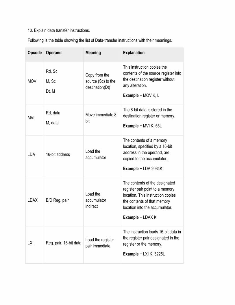
10. Explain data transfer instructions.
Following is the table showing the list of Data-transfer instructions with their meanings.
Opcode Operand Meaning Explanation
MOV
Rd, Sc
M, Sc
Dt, M
Copy from the
source (Sc) to the
destination(Dt)
This instruction copies the
contents of the source register into
the destination register without
any alteration.
Example − MOV K, L
MVI Rd, data
M, data
Move immediate 8-
bit
The 8-bit data is stored in the
destination register or memory.
Example − MVI K, 55L
LDA 16-bit address Load the
accumulator
The contents of a memory
location, specified by a 16-bit
address in the operand, are
copied to the accumulator.
Example − LDA 2034K
LDAX B/D Reg. pair
Load the
accumulator
indirect
The contents of the designated
register pair point to a memory
location. This instruction copies
the contents of that memory
location into the accumulator.
Example − LDAX K
LXI Reg. pair, 16-bit data Load the register
pair immediate
The instruction loads 16-bit data in
the register pair designated in the
register or the memory.
Example − LXI K, 3225L

LHLD 16-bit address Load H and L
registers direct
The instruction copies the
contents of the memory location
pointed out by the address into
register L and copies the contents
of the next memory location into
register H.
Example − LHLD 3225K
STA 16-bit address 16-bit address
The contents of the accumulator
are copied into the memory
location specified by the operand.
This is a 3-byte instruction, the
second byte specifies the low-
order address and the third byte
specifies the high-order address.
Example − STA 325K
STAX 16-bit address
Store the
accumulator
indirect
The contents of the accumulator
are copied into the memory
location specified by the contents
of the operand.
Example − STAX K
SHLD 16-bit address Store H and L
registers direct
The contents of register L are
stored in the memory location
specified by the 16-bit address in
the operand and the contents of H
register are stored into the next
memory location by incrementing
the operand.
This is a 3-byte instruction, the
second byte specifies the low-
order address and the third byte
specifies the high-order address.

Example − SHLD 3225K
XCHG None Exchange H and L
with D and E
The contents of register H are
exchanged with the contents of
register D, and the contents of
register L are exchanged with the
contents of register E.
Example − XCHG
SPHL None
Copy H and L
registers to the
stack pointer
The instruction loads the contents
of the H and L registers into the
stack pointer register. The
contents of the H register provide
the high-order address and the
contents of the L register provide
the low-order address.
Example − SPHL
XTHL None Exchange H and L
with top of stack
The contents of the L register are
exchanged with the stack location
pointed out by the contents of the
stack pointer register.
The contents of the H register are
exchanged with the next stack
location (SP+1).
Example − XTHL
PUSH Reg. pair Push the register
pair onto the stack
The contents of the register pair
designated in the operand are
copied onto the stack in the
following sequence.
The stack pointer register is
decremented and the contents of
the high order register (B, D, H, A)
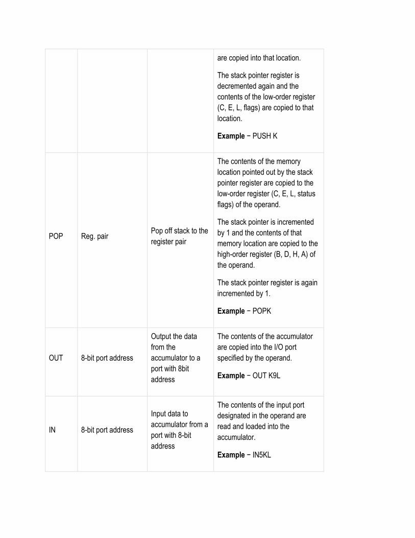
are copied into that location.
The stack pointer register is
decremented again and the
contents of the low-order register
(C, E, L, flags) are copied to that
location.
Example − PUSH K
POP Reg. pair Pop off stack to the
register pair
The contents of the memory
location pointed out by the stack
pointer register are copied to the
low-order register (C, E, L, status
flags) of the operand.
The stack pointer is incremented
by 1 and the contents of that
memory location are copied to the
high-order register (B, D, H, A) of
the operand.
The stack pointer register is again
incremented by 1.
Example − POPK
OUT 8-bit port address
Output the data
from the
accumulator to a
port with 8bit
address
The contents of the accumulator
are copied into the I/O port
specified by the operand.
Example − OUT K9L
IN 8-bit port address
Input data to
accumulator from a
port with 8-bit
address
The contents of the input port
designated in the operand are
read and loaded into the
accumulator.
Example − IN5KL

11. Explain in detail about interrupts.
Interrupts in 8085
Interrupts are the signals generated by the external devices to request the microprocessor to perform a
task. There are 5 interrupt signals, i.e. TRAP, RST 7.5, RST 6.5, RST 5.5, and INTR.
Interrupt are classified into following groups based on their parameter −
Vector interrupt − In this type of interrupt, the interrupt address is known to the processor. For
example: RST7.5, RST6.5, RST5.5, TRAP.
Non-Vector interrupt − In this type of interrupt, the interrupt address is not known to the processor
so, the interrupt address needs to be sent externally by the device to perform interrupts. For
example: INTR.
Maskable interrupt − In this type of interrupt, we can disable the interrupt by writing some
instructions into the program. For example:RST7.5, RST6.5, RST5.5.
Non-Maskable interrupt − In this type of interrupt, we cannot disable the interrupt by writing some
instructions into the program. For example: TRAP.
Software interrupt − In this type of interrupt, the programmer has to add the instructions into the
program to execute the interrupt. There are 8 software interrupts in 8085, i.e. RST0, RST1, RST2,
RST3, RST4, RST5, RST6, and RST7.
Hardware interrupt − There are 5 interrupt pins in 8085 used as hardware interrupts, i.e. TRAP,
RST7.5, RST6.5, RST5.5, INTA.
Note − NTA is not an interrupt, it is used by the microprocessor for sending acknowledgement. TRAP has
the highest priority, then RST7.5 and so on.
Interrupt Service Routine (ISR)
A small program or a routine that when executed, services the corresponding interrupting source is called
an ISR.
TRAP
It is a non-maskable interrupt, having the highest priority among all interrupts. Bydefault, it is enabled until it
gets acknowledged. In case of failure, it executes as ISR and sends the data to backup memory. This
interrupt transfers the control to the location 0024H.
RST7.5

It is a maskable interrupt, having the second highest priority among all interrupts. When this interrupt is
executed, the processor saves the content of the PC register into the stack and branches to 003CH
address.
RST 6.5
It is a maskable interrupt, having the third highest priority among all interrupts. When this interrupt is
executed, the processor saves the content of the PC register into the stack and branches to 0034H
address.
RST 5.5
It is a maskable interrupt. When this interrupt is executed, the processor saves the content of the PC
register into the stack and branches to 002CH address.
INTR
It is a maskable interrupt, having the lowest priority among all interrupts. It can be disabled by resetting the
microprocessor.
When INTR signal goes high, the following events can occur −
The microprocessor checks the status of INTR signal during the execution of each instruction.
When the INTR signal is high, then the microprocessor completes its current instruction and sends
active low interrupt acknowledge signal.
When instructions are received, then the microprocessor saves the address of the next instruction
on stack and executes the received instruction.
12. Explain about the architecture of microcontroller.
8051 microcontroller is designed by Intel in 1981. It is an 8-bit microcontroller. It is built with 40 pins DIP
(dual inline package), 4kb of ROM storage and 128 bytes of RAM storage, 2 16-bit timers. It consists of are
four parallel 8-bit ports, which are programmable as well as addressable as per the requirement. An on-
chip crystal oscillator is integrated in the microcontroller having crystal frequency of 12 MHz.
Let us now discuss the architecture of 8051 Microcontroller.
In the following diagram, the system bus connects all the support devices to the CPU. The system bus
consists of an 8-bit data bus, a 16-bit address bus and bus control signals. All other devices like program
memory, ports, data memory, serial interface, interrupt control, timers, and the CPU are all interfaced
together through the system bus.

13. Explain the pin configuration of 8051 microcontroller.
The pin diagram of 8051 microcontroller looks as follows −
Pins 1 to 8 − These pins are known as Port 1. This port doesn’t serve any other functions. It is
internally pulled up, bi-directional I/O port.
Pin 9 − It is a RESET pin, which is used to reset the microcontroller to its initial values.
Pins 10 to 17 − These pins are known as Port 3. This port serves some functions like interrupts,
timer input, control signals, serial communication signals RxD and TxD, etc.
Pins 18 & 19 − These pins are used for interfacing an external crystal to get the system clock.
Pin 20 − This pin provides the power supply to the circuit.
Pins 21 to 28 − These pins are known as Port 2. It serves as I/O port. Higher order address bus
signals are also multiplexed using this port.
Pin 29 − This is PSEN pin which stands for Program Store Enable. It is used to read a signal from
the external program memory.
Pin 30 − This is EA pin which stands for External Access input. It is used to enable/disable the
external memory interfacing.
Pin 31 − This is ALE pin which stands for Address Latch Enable. It is used to demultiplex the
address-data signal of port.
Pins 32 to 39 − These pins are known as Port 0. It serves as I/O port. Lower order address and
data bus signals are multiplexed using this port.
Pin 40 − This pin is used to provide power supply to the circuit.
14. Explain about the 8051 interrupts.
Interrupts are the events that temporarily suspend the main program, pass the control to the external
sources and execute their task. It then passes the control to the main program where it had left off.
8051 has 5 interrupt signals, i.e. INT0, TFO, INTR1, TF1, RI/TI. Each interrupt can be enabled or disabled
by setting bits of the IE register and the whole interrupt system can be disabled by clearing the EA bit of the
same register.
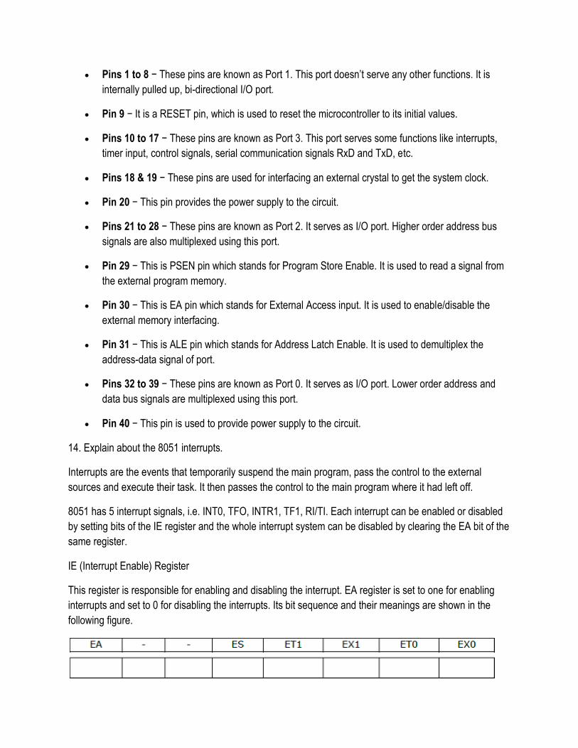
IE (Interrupt Enable) Register
This register is responsible for enabling and disabling the interrupt. EA register is set to one for enabling
interrupts and set to 0 for disabling the interrupts. Its bit sequence and their meanings are shown in the
following figure.
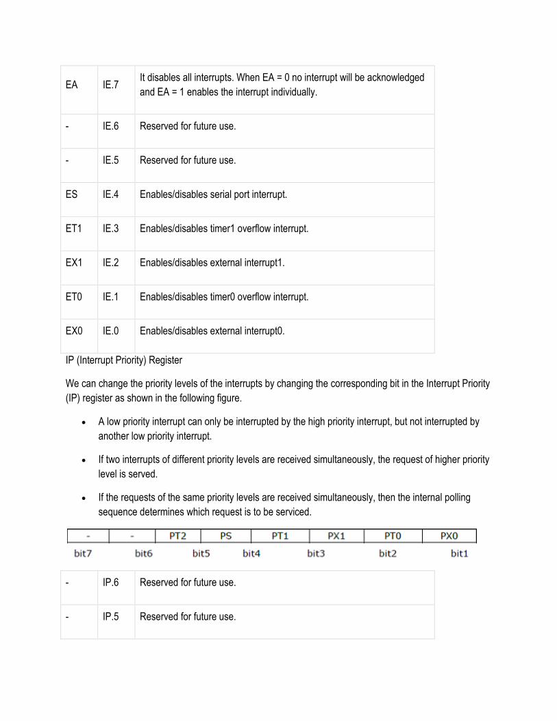
EA IE.7 It disables all interrupts. When EA = 0 no interrupt will be acknowledged
and EA = 1 enables the interrupt individually.
- IE.6 Reserved for future use.
- IE.5 Reserved for future use.
ES IE.4 Enables/disables serial port interrupt.
ET1 IE.3 Enables/disables timer1 overflow interrupt.
EX1 IE.2 Enables/disables external interrupt1.
ET0 IE.1 Enables/disables timer0 overflow interrupt.
EX0 IE.0 Enables/disables external interrupt0.
IP (Interrupt Priority) Register
We can change the priority levels of the interrupts by changing the corresponding bit in the Interrupt Priority
(IP) register as shown in the following figure.
A low priority interrupt can only be interrupted by the high priority interrupt, but not interrupted by
another low priority interrupt.
If two interrupts of different priority levels are received simultaneously, the request of higher priority
level is served.
If the requests of the same priority levels are received simultaneously, then the internal polling
sequence determines which request is to be serviced.
- IP.6 Reserved for future use.
- IP.5 Reserved for future use.
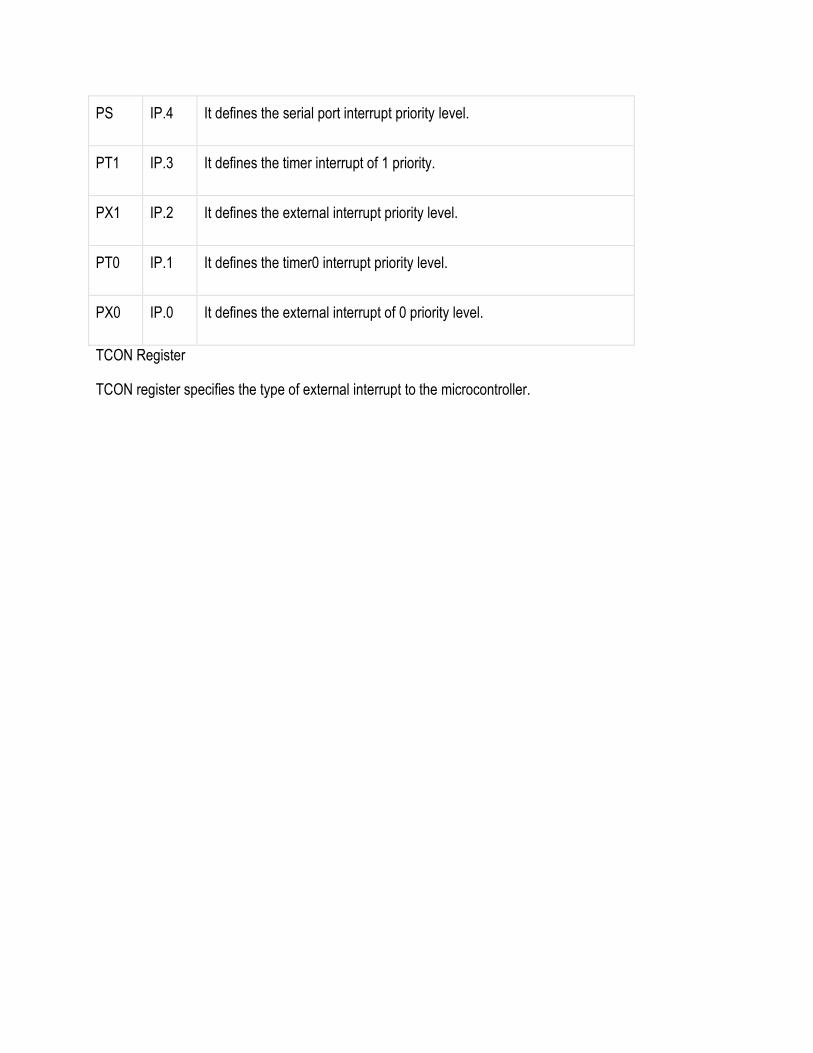
PS IP.4 It defines the serial port interrupt priority level.
PT1 IP.3 It defines the timer interrupt of 1 priority.
PX1 IP.2 It defines the external interrupt priority level.
PT0 IP.1 It defines the timer0 interrupt priority level.
PX0 IP.0 It defines the external interrupt of 0 priority level.
TCON Register
TCON register specifies the type of external interrupt to the microcontroller.