3-1 section 2 computational unit dsp 技术与应用. 3-2 adsp-219x block diagram 160 mhz up to 64k...
TRANSCRIPT

3-1
Section 2
Computational Unit
DSP技术与应用

3-2
ADSP-219x Block Diagram160 MHz
Up to 64K words RAM
16K words ROM optional
Boot ROM
Multi-channel serial ports
SPI and UART Ports
Three 32-bit timers with PWM outputs
8- or 16-bit host port interface
External memory interface
Up to 16 general purpose I/O
11 channel DMA controller
On chip oscillator with PLL
Flexible power management
JTAG port for system test & debug
Industrial grade
144 BGA and QFP packages16 GPIO
Timers
SPI
8/16/32KRAM
InterruptController
System Clock (PLL)
Power DownControl
Serial Port
JTAG Scan
ParallelPort
DMAController
UART
ADSP-219x16-bit Core
16-bit Memory
Host Port
Serial Port
Serial Port
SPI
16K x 24ROM
8/16/32KRAM
24-bit Memory

3-3
ADSP-219x Memory Maps
Simple migration from ADSP-2191 RAM device to low cost ROM devices
Pin-Pin compatible models allow users to:
migrate to smaller memory to reduce system costs or
move to larger memory models to increase end-product functionality
16K x 24 ROM
16K x 24 RAM
16K x 16 RAM
Ext
ern
al M
emo
ry I
nte
rfac
e
ADSP-2195
16K x 24 ROM
8K x 24 RAM
ADSP-2196
8K x 16 RAM
Ext
ern
al M
emo
ry I
nte
rfac
e
32K x 24 RAM
32K x16 RAM
ADSP-2191
Ext
ern
al M
emo
ry I
nte
rfac
e

3-4
ADSP-219x Block Diagram

3-5
ADSP-2191 DSP Core Features• Fast arithmetic processing capabilities
– Register File, ALU, Multiplier/MAC, Shifter• Single cycle arithmetic operations• No arithmetic Pipelining:
– Register File -to- Arithmetic -to- Register File within one instruction cycle
• Multiplier/MAC, Shifter support 40 bit results• Single-cycle Multiple data transfers
– Two independent Data Address Generators (DAGs) support multiple data accesses in a single cycle
• Circular buffer addressing supported in hardware– Both DAGs support circular buffering
• Efficient program execution– Fast and efficient Program Sequencer– Supports looping in hardware, 8 levels deep

3-6
DSP Core
Cache
Data Memory Data Program Memory Data
Data Memory Address
Program Memory Address
Internal Memory
Modified Harvard Architecture
• Instructions are fetched over the PM bus unless in cache• Data Memory accesses have precedence over Program Memory data
accesses • PM Bus conflicts occur when instruction fetch and PM data fetch are
required in the same cycle (cache miss) • Block conflicts occur when both buses want to go to the same block in the
SAME cycle
24
24
24
16

3-7
How does the ADSP-2191 process it?
I0=values;I4=constants;M0=1;M4=1;
MR=0, MX0=dm(I0,M0), MY0=pm(I4,M4);
cntr=1023; do myloop until ce;
myloop: MR=MR+MX0*MY0(SS), MX0=dm(I0,M0), MY0=pm(I4,M4);
MR=MR+MX0*MY0(SS);
Harvard Architecture Allows Dual Data Fetch with implicit Pointer Updates in parallel
Loop Control Hardware avoids software overhead
Multiplication, Accumulation and Data Load in a real single cycle
32-Bit Multiplier Result Accumulation into a 40-Bit Register avoids need of overflow handling during loop

3-8
Computational Units
Section 2

3-9
Binary Number Formatting

3-10
Binary Notation in DSP's
The ADSP-2100 Family of DSP's are fixed point processors thatperform operations using a two's complement binary notation.Therefore, to efficiently program a DSP it is important to understand the following concepts:
1) Signed / Unsigned formats
2) Fractional / Integer formats
3) Ranges of Fractional Numbers
4) Hex to Decimal Conversions
5) Decimal to Hex Conversions

3-11
Binary - Hexadecimal - Decimal Number Conversion Table
Decimal
0 123456789
101112131415
Hexadecimal
01 23456789ABCDEF
Binary
0000 000100100011010001010110011110001001101010111100110111101111

3-12
Example of Data Formats
Unsigned
Signed
0x0000 0V (- FULL SCALE)
0xFFFF 5V (+ FULL SCALE)
0x8000 -5V (- FULL SCALE) 0x0000 0V
0x7FFF 5V (+ FULL SCALE)
S/U U U U U U U U U U U U U U U U
015
Binary Bit Pattern Example System
16 Bits of Data
3-13
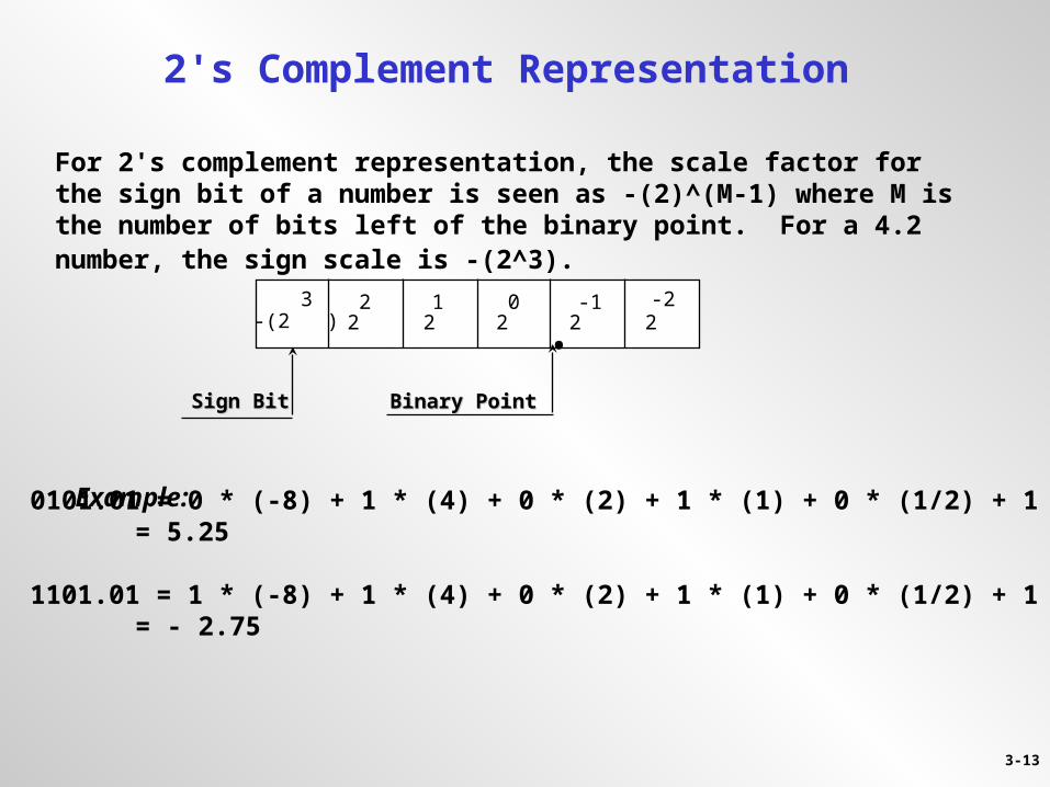
2's Complement Representation
For 2's complement representation, the scale factor for the sign bit of a number is seen as -(2)^(M-1) where M is the number of bits left of the binary point. For a 4.2 number, the sign scale is -(2^3).
Example: 0101.01 = 0 * (-8) + 1 * (4) + 0 * (2) + 1 * (1) + 0 * (1/2) + 1 * (1/4) = 5.25
1101.01 = 1 * (-8) + 1 * (4) + 0 * (2) + 1 * (1) + 0 * (1/2) + 1 * (1/4)= - 2.75
Binary PointBinary Point
-2-13 012-(2 ) 2 2 2 2 2
Sign BitSign Bit
.

3-14
2's Complement Representation
Changing the sign of a 2‘s Complement Number
-X = NOT(X) + 1 LSB ( invert all the bits and add an LSB)
Example:
-5.25 = -(b#0101.01) = NOT(b#0101.01) + b#0000.01 = b#1010.10 + b#0000.01 = b#1010.11
1010.11 = 1 * (-8) + 0 * (4) + 1 * (2) + 0 * (1) + 1 * (1/2) + 1 * (1/4) = -5.25

3-15
Fractional versus Integer Notation
• Fractional format is 1.15 notation
S F F F F F F F F F F F F F F F•
S I I I I I I I I I I I I I I I•
radix point
radix point
• Integer format is 16.0 notation

3-16
DSP is optimized for fractional notation
DSP supports integer notation

3-17
16位定点数的m,n表示法
m表示符号位和整数部分, n表示小数部分,且m+n=16
因此数的整数范围为( -2m-1,2m-1 ),小数的最小分辨率为 2-n
ADSP-219X在乘法运算时使用 1.15表示小数使用 16.0表示整数

3-18
Ranges for 16 bit Formats
Largest Positive Value (0x7FFF)
In Decimal
0.999969482421875 1.999938964843750 3.999877929687500 7.999755859375000
15.999511718750000 31.999023437500000 63.998046875000000
127.996093750000000 255.992187500000000 511.984375000000000
1023.968750000000000 2047.937500000000000 4095.875000000000000 8191.750000000000000
16383.500000000000000 32767.000000000000000
Largest Negative Value (0x8000)
In Decimal
–1.0 –2.0 –4.0 –8.0
–16.0 –32.0 –64.0
–128.0 –256.0 –512.0
–1024.0 –2048.0 –4096.0 –8192.0
–16384.0 –32768.0
Value of 1 LSB (0x0001) In Decimal 0.000030517578125 0.000061035156250 0.000122070312500 0.000244140625000 0.000488281250000 0.000976562500000 0.001953125000000 0.003906250000000 0.007812500000000 0.015625000000000 0.031250000000000 0.062500000000000 0.125000000000000 0.250000000000000 0.500000000000000 1.000000000000000
FORMAT 1.15 2.14 3.13 4.12 5.11 6.10 7.9 8.8 9.7 10.6 11.5 12.4 13.3 14.2 15.1 16.0
Fractional
Integer

3-19
Format Example
+5 V
-5 V
0 V
0x7FFF
0x0000
0x8000
1 2
3
4 5
FORMAT
0x7FFF 0x3FFF 0x0000 0xCCCD 0x8000
1) 2) 3) 4) 5)
16.0 1.15
5 V 2.5 V 0 V -2.0 V -5.0 V
= 32767 -> = 16383 -> = 0 -> = -13107 -> = -32768 ->
0.999969482... -> 0.499969482... -> 0.0000000... -> -0.399993986... -> -1.0000000.... ->
5 V 2.5 V 0 V -2.0 V -5.0 V

3-20
There are two methods for converting hexadecimal numbers to decimal numbers. One is easy and one is hard.
HARD WAY: Convert the hexadecimal number to binary. Place the binary point. Multiply each bit of the binary number by its associated scale factor.
Example: Convert 0x2A00 to a 1.15 twos-complement decimal value
0x2A00 = 0.010 1010 0000 0000 = 2^-2 + 2^-4 + 2^-6 = 0.25 + 0.0625 + 0.015625 = 0.328125 = 0.33 = 1/3
EASY WAY: Use a calculator to convert the hexadecimal number to decimal. Divide the decimal number by 2^N where N is the number of bits to the right of the binary point.
Example: Convert 0x2A00 to a 1.15 twos-complement decimal value0x2A00 <=> 10752 / 2^15 = 10752 / 32768 = 0.328125
Hexadecimal to Decimal Conversion (1.15 Format)

3-21
There are two methods for converting Decimal Numbers to Hexadecimal numbers. One is easy, and one is hard.
HARD WAY: Break the decimal number into its 2^N components.
Example: Convert 0.8125 to a 1.15 twos-complement hexadecimal format.
EASY WAY: Multiply the decimal number by 2^N where N is the number of bits to the right of the binary point. Then use a calculator to convert to hex.
Example: Convert 0.8125 to a 1.15 twos-complement hexadecimal format0.8125 * 2^15 = 0.8125 * 32768 = 26624 <=> 0x6800
0.8125 =>
2-2
2-1
20
2-3
2-4
2-5
2-6
2-7
1 1/2 1/4 1/8 1/16 1/641/32 1/128
0 0001011 => 0x6800
Decimal to Hexadecimal Conversion (1.15 Format)

3-22
Binary Notation Mini-Quiz
What is 0x4000 (1.15 format) in signed decimal notation?
What is 0x4000 (16.0 format) in signed decimal notation?
What is 0x4000 (0.16 format) in unsigned decimal notation?
What is .875 in hex 1.15 Format?
What is -.875 in hex 1.15 Format?

3-23
Registers and Register File

3-24
Register Groups
Register File (DREG) Data Address GeneratorInterrupt RegistersBus Exchange (Px)Program SequencerPage RegistersStatus Registers
DAG Base Address Registers
Cache Control Register (CACTL)
System Control Registers(memory mapped)
Use ‘reg(<addr>)’ to access
Core RegistersName explicitly to access
System Control Registers
DMA Controller Registers
Serial Port (SPORT)
SPI Port
EMI Registers
Timer
I/O Processor Registers(memory mapped)
Use ‘io(<addr>)’ to access

3-25
Core Register Subgroups
Arranged in logical groups to facilitate general instruction coding DREG => data registers G1REG => DAG1, interrupt control registers G2REG => DAG2, loop counter registers G3REG => status, page registers
Arranged in smaller logical groups for conditional instruction coding XOPs and YOPs => specific subsets of DREG depending on
type of computation unit (ALU/MAC/SHIFTER) XOP => X operand for computational units YOP => Y operand for computational units

3-26
ADSP-219x Block Diagram

3-27
Register File
Input onlyMX0 MX1 AX0 AX1
MY0 MY1 AY0 AY1 SIOutput/Input
MR2 MR1 MR0 ARSR2 SR1 SR0
Input onlyMX0 MX1 AX0 AX1
MY0 MY1 AY0 AY1 SIOutput/Input
MR2 MR1 MR0 ARSR2 SR1 SR0
The register file is the source and destination for most arithmetic operations
16 x 16 bit registers Complete set of background registers

3-28
Computational Registers
16 x 16 Computational Registers in Register File (dreg)
AR, AX0, AY0, AX1, AY1
MR2, MR1, MR0, MX0, MY0, MX1, MY1
SR2, SR1, SR0, SI Additional Special Purpose Computational Registers
AF ALU feedback, intermediate ALU results
SE Shifter Exponent
SB Shifter Block Exponent Status Registers
ASTAT Arithmetic Status
MSTAT Mode Status

3-29
Mode Status (MSTAT) Register

3-30
Arithmetic Status (ASTAT) Register

3-31
Register Access—Unconditional, Single-Function Instructions

3-32
ADSP-219x Block Diagram

3-33
Arithmetic Logic Unit (ALU)
ARRegister
In Register file
ARRegister
In Register file
ALU
MUX
CI
AR SATAV LATCH
AZANACAVASAQ
1616
AFRegister
16
From Register File
X Y
16
16

3-34
Arithmetic Logic Unit ( ALU )
• Basic arithmetic – addition, subtraction, add or subtract by a constant, increment/decrement, etc.
• Logical operations – AND, OR, XOR, NOT.• Bit tests.• ABS, PASS, Division Primitives
• Supports conditional instructions • Support for multiprecision math
Features
Functions

3-35
Arithmetic Logic Unit ( ALU )Example Instructions
AR = MX0 +AY0; // Add the values in MX0 and AY0. Result is stored in AR
AF = MR1 XOR AY1; // Perform an XOR with MR1 and AY1. Result is stored in AF
IF GE AR = -AR; // Conditional instruction – if the previous ALU // operation resulted in a value greater than or equal // to zero, neg. AR.
IF AV AR = AY1 +1; // Conditional instruction –overflow occurs flag is set, // increment the value in AY1.
AR = MY0 + MY0; // The value of one register can be added by it self.
AF = MY0 + MR1 + C; // Add the values MY0 and MR1 in respect of the carry // flag.
AR = AX0 + AF; // Add the values in AX0 and AF. Store the result in AR
// This instructions uses the XOP and YOP register subsets
• AF is not in the register file. Must follow ALU conditional instruction register usage
• The destination of the ALU result is either the AR or AF register. Only the specified destination register is updated

3-36
Arithmetic Logic Unit ( ALU )
Unconditional ALU Instructions: Any register (DREGx) in the register file can be used as input
AR = DREG1 + DREG2 ;AF DREG1 + C ; DREG1 + DREG2 + C ; DREG1 - DREG2 ; DREG1 - DREG2 + C - 1 ;
DREG1 AND DREG2 ; DREG1 OR DREG2 ; DREG1 XOR DREG2 ; NOT DREG ;
PASS DREG1 ;
LogicalOperations
// Pass through ALU, set flags
// Add // Add with carry
// Subtract
// Subtract with borrow
// Add with carry
DREG1, DREG2 = DREG register set

3-37
Arithmetic Logic Unit ( ALU ) Conditional ALU Instructions:[IF condition] AR = xop + yop ; AF xop + C ;
xop + yop + C ; xop - yop ; xop - yop + C - 1 ;
yop - xop ; yop - xop + C - 1 ;
[IF condition] AR = xop AND yop; AF xop OR yop;
xop XOR yop; NOT xop ; NOT yop ;
[IF condition] AR = PASS xop ; AF yop ;
constant ;
xop + yop ;
xop = AX0, AX1, AR, MR0, MR1, MR2, SR0, SR1 yop = AY0, AY1, AF, 0
LogicalOperations
// Pass XOP through ALU, set flags
// Pass YOP through ALU, set flags
// Pass a constant through ALU // to affect the status flags
// Add
// Add with carry
// Subtract
// Subtract with borrow
// Add with carry
// addition updates the status flags
// Subtract yop/xop exchanged
// Subtract with borrow

3-38
Arithmetic Logic Unit ( ALU )[IF condition] AR = - xop ;
AF - yop ; ABS xop ; yop +/- 1 ;
DIVS yop , xop ;DIVQ xop ;
[IF condition] AR = TSTBIT n of xop; AF SETBIT
CLRBIT TGLBIT
n = [0, 1, 2, 3, 4, 5, 6, 7, 8, 9, 10, 11, 12, 13, 14, 15]
[IF condition] AR = xop function constant; AF
function = [+, -, AND, OR, XOR, NOT, ABS,PASS]constant = [0, 1, 2, 4, 8, 16, 32, 64, 128, 256, 512, 1024, 2048, 4096, 8192, 16384, 32767, -2,
-3, -5, -9, -17, -33, -65, -129, -257, -513, -1025, -2049, -4097, -8193, -16385, -32768]
// makes the 2‘s complement of xop. // makes the 2‘s complement of yop.
// division operation see advanced// instructions.
// absolute value of xop.// increment/decrement of yop.
// tests or modifies the bit n of the // register xop.
// ALU operations using // constants.

3-39
Arithmetic Status Register ASTATALU Flags
Quotient bit generated only by DIVS and DIVQ
QuotientAQ
Sign of ALU input port. Affected only by ABS instruction
SignAS
Carry output from most significant adder stage
CarryAC
X-OR of carry outputs of 2 most significant adder stages. True if ALU overflows
OverflowAV
Sign bit of ALU result. True if ALU output negative
NegativeAN
True if ALU output equals 0ZeroAZ
DefinitionNameFlag

3-40
Arithmetic Logic Unit ( ALU ) condition codes
Condition Description
EQ Equal to zero (=0).
NE Not equal to zero (!=0).
GT Greater than zero (>0).
LE Less than or equal to zero (<=0).
LT Less than zero (<0).
GE Greater than or equal to zero (>=0).
AV ALU overflow.
NOT AV Not ALU overflow.
AC ALU carry.
NOT AC Not ALU carry.
SWCOND SWCOND (based on CCODE register condition).
NOT SWCOND Not SWCOND (based on CCODE register condition).
MV MAC overflow.
NOT MV Not MAC overflow.
NOT CE Counter not expired.
TRUE Always true.
Condition codes
are based on values in
ASTAT

3-41
Arithmetic Logic Unit ( ALU ) Saturation
Sets ALU result to full scale positive or full scale negative if overflow or underflow occurs
Saturation mode enabled by executing ‘ena ar_sat or ena AS’ (bit 3 of MSTAT)
Once enabled, affects every ALU operation with AR as the destination
AF will not saturate, (flags still get set)
Overflow or underflow determined by the following conditions
Overflow (AV) carry (AC) AR contents
0 0 ALU output
0 1 ALU output
1 0 0x7fff full-scale positive
1 1 0x8000 full-scale negative

3-42
Making the AV Flag Sticky
• The ALU overflow flag AV can become a sticky flag by setting bit 2 in MSTAT– Making the AV flag sticky means once it is set it stays set
until you explicitly clear it in software
• Enable this feature by executing the instruction
“ena av_latch” or “ena OL”• Disable this feature by executing the instruction
“dis av_latch” or “ena OL”
You can also write or read MSTAT directly

3-43
Go to ALU Exercises

3-44
ADSP-219x Block Diagram

3-45
Multiply-Accumulator (MAC)
Multiplier
16
MV or SV
ADD/Sub
40
16
40
SR2 | SR1 | SR0 Register File
MR2 | MR1 | MR0 or
From Register File
32

3-46
Multiply-Accumulator (MAC)
• Multiplication• Multiplication/accumulate with addition, rounding optional• Multiplication/accumulate with subtraction, rounding optional• Rounding, saturating, or clearing result register
Features
Functions
• 40-bit dual accumulator registers (The result can either be put in register MR or register SR)
• Multifunction computations can perform a MAC and load/store operations in a single cycle.
• 8 bits of overflow protection (255 consecutive full-scale accumulates )• Fractional & Integer support• Instructions can be conditional• Single-cycle context switch

3-47
Example MAC Instructions
MR = MX1 * MY0(SS); // multiply the value in MX1 and in MY0. Store the // result in the MR register.
SR = AR * MY1(SS); // multiply the value in AR and MY1. Store the result
// in the SR register.
MR = MR + AR * MY1(SS); // multiply the value in AR and MY1 and add this // result to the previous value in MR.
MR = 0; // clear the MR Accumulator and MV
SAT MR; // Saturate MR if overflow flag was set.
MR = MR; // can be used to effect the status flags (Check MV)
IF EQ MR = MX0 * MY0(UU); // conditional instruction. If zero flag set by last ALU // operation, then condition true

3-48
Unconditional MAC Instructions
Multiply
MR = DREG1 * DREG2 ( RND ) ;
SR SS
SU
US
UU
Multiply with Add/Subtract
MR = MR DREG1 * DREG2 ( RND ) ;
SR = SR SS
SU
US
UU
Any register (DREGx) in the register file can be used as input
S = Signed
U = Unsigned
RND = Round
+-

3-49
Conditional MAC Instructions
Multiply
[IF condition] MR = XOP * YOP ( RND ) ;
SR XOP SS
SU
US
UU
Multiply with Add/Subtract
[IF condition] MR = MR XOP * YOP ( RND ) ;
SR = SR YOP XOP SS
SU
US
UU
S = Signed
U = Unsigned
RND = Round
XOP = MX0, MX1, AR, MR0, MR1, MR2, SR0, SR1YOP = MY0, MY1, SR1, 0
+-

3-50
Binary Integer Multiplication
M Bits
P Bitsx
M+P Bits
Example: 16.0 x 16.0 => 32.0
Mixed/Fractional Multiplication
M.N Bits
P.Q Bitsx
(M+P).(N+Q) Bits
Example: 1.15 x 1.15 => 2.30** 4.12 x 1.15 => 5.27
** In fractional mode the result of a multiplication will be automatically left shifted by 1 bit resulting in a 1.31 format
Placement of Binary Point in Multiplication

3-51
S.OVERFLOW
MR2/SR2 MR1/SR1 MR0/SR0
Sign Bit
Most Significant16 Bits
Least Significant16 Bits
S
OVERFLOW
MR2/SR2 MR1/SR1 MR0/SR0
Sign Bit
Most Significant16 Bits
Least Significant16 Bits
.
FractionalMode
IntegerMode
Placement of Sign Bit in MR/SR

3-52
0x4000 0x4000
MX0 MY1
MR0MR1MR2
MR1
0x00 2000 0000
0x2000 underflowoverflow
=0.5 =0.5
=0.25
Multiplication Modes on the ADSP-219x
• Mode 1: Fractional Mode
• Multiplier assumes all numbers in a 1.15 format
• Multiplier automatically shifts product 1-bit left before accumulation (result forced to 1.31 format)
• Example: MR = MX0 * MY1 (SS);
1.15 Format

3-53
0x4000 0x4000
MX0 MY1
MR0MR1MR2
0x00 1000 0000
0x0000overflow
MR0
overflow
=2 =2
=2
14 14
28
Multiplication Modes on the ADSP-219x
• Mode 2: Integer Mode
• Multiplier assumes all numbers in a 16.0 format
• No automatic left-shift necessary
• Example: MR = MX0 * MY1 (SS);

3-54
Selecting Between Integer and Fractional Modes
• Selecting Between Fractional and Integer Modes– Bit 4 of the MSTAT register determines multiplication mode
• 0 = Fractional Mode (default), 1 = Integer Mode– There are dedicated instructions to set and clear bit 4 of
MSTAT• ENA M_MODE or ENA MM, sets bit 4 to 1(integer mode)• DIS M_MODE or DIS MM, sets bit 4 to 0 (fractional mode)• No effect latency when using ENA or DIS instruction
• MSTAT can be read and written any time– MSTAT=0x10; (one cycle effect latency)
Note: Check users manual for latencies on other MSTAT bits

3-55
Rounding/Saturation in the MAC
• Rounding operation—MR/SR=MR/SR (Rnd)—should only be used with fractional results. Round corrupts MR0
• This explicit rounding operation generates the same results as using the Rnd option in other multiplier instructions.
• Saturate operation—Sat MR/SR—sets the specified result register to the maximum positive or negative value if an overflow or underflow has occurred.

3-56
Rounding in the MAC
• Rounding can be specified as part of multiply instruction (RND)
• Rounding only applies to fixed-point signed fractional results
• 40-bit results "rounded to nearest" 16 bit value.
• Rounded result can be placed in MR or SR register
Input: MX0 = 0x7FF9, MY0 = 0xEEEE
Command MR2 MR1 MR0
MR = MX0 * MY0 (SS); FF EEEE EEFC
MR = MX0 * MY0 (RND); FF EEEF 6EFC
• ADSP-219x Support a “Biased” Rounding
– When MR0 = 0x8000, will always round up
– Enabled by setting BIASRND bit (bit 7 of the ICNTL Register)
– Useful for GSM speech coding where biased rounding is specified

3-57
Saturation
• The SAT instruction checks the value of MR or SR to determine when to saturate– Checks to see if upper 9 bits of MR or SR are equal
• Saturation is performed by following instruction:
SAT MR; or SAT SR;
Input: MX0 = 0x7FFF, MY0 = 0x7FFF, MR = 00 7FFE 0002
Command MR2 MR1 MR0
MR = MR + MX0 * MY0 (SS); 0000 FFFC 0004
SAT MR; 0000 7FFF FFFF

3-58
Multiplier Bits in ASTAT
• The MV Bit is set when the multiplier result destination is MR and an overflow has occurred– MR overflow, Bit 6 of ASTAT
• SV Bit is set when the multiplier result destination is SR and an overflow has occurred– SR overflow, Bit 8 of ASTAT
• Overflow occurs when sign bit is corrupted during accumulation
• Overflow Status (MV or SV) is updated every time a MAC operation is executed
• MV or SV is set when any bits of significance cross into MR2– Can be seen when bits in MR2 do not equal MSB of MR1
• MR2 or SR2 will automatically sign extend– Writes to MR1 or SR1 will automatically sign extend into MR2 or
SR2

3-59
Go to Multiplier Exercises

3-60
ADSP-219x Block Diagram

3-61
ADSP-2191 Barrel Shifter
SHIFTERSV
MUX
40
SERegister
16
OR / PASS40
SR2 | SR1 | SR0 Register File
SBRegister
Exponent Detector
COMPARE
SS
HI / LO
X
NEGATE
from Instruction
8
40
From Register File

3-62
Barrel Shifter
Functions Logical & Arithmetic shift (Ashift/Lshift) Normalization (Norm) Derivation of Exponent (Exp) Exponent Adjust (block floating point) (Expadj)
Features 16 bit input value gets shifted and stored anywhere in a 40 bit
output field in a single cycle Shift value can be specified immediately within the instruction
or indirectly using the SE register Normalize, de-normalize, and exponent detect instructions
used for block floating point and floating point operations

3-63
Shift Types
There are two types of shifts:
Arithmetic shift (ASHIFT), on right shifts the vacated bits to the left are sign extended, and zero filled to the right
This will preserve sign information
Logical Shift (LSHIFT), on right shifts the vacated bits to the left are zero filled, and zero filled to the right
Used for packing bit patterns Example: saving two 8 bit words in a 16 bit register

3-64
ADSP-2191 Barrel Shifter (Instruction)
Arithmetic (ASHIFT) Shift vs. Logic (LSHIFT) Shift– Arithmetic shifts sign extend right shifts
This will preserve sign information– Logical shift zero fills right shifts
Used for packing bit patterns– Left shifts are always zero filled
Positive SE or <data> values shift left Negative SE or <data> values shift right NO explicit "+" for positive shifts required Placement of output depends on HI/LO modifier, SE register
and <data> value

3-65
Example Barrel Shifter Instructions
SR = ASHIFT SI BY –12 (HI); // arithmetic shift of the input SI 12 // bits right. Result is placed in SR
SR = LSHIFT AR BY 6 (HI); // logical shift of the input AR 6 // bits left. Result is placed in SR
SR = SR OR LSHIFT AX0 (LO); // Shift the content of AX0 by SE, OR it with // the current value of SR, update SR
IF EQ SR = ASHIFT MY1 (LO); // Conditional ASHIFT of MY1, by the value // in SE, store the result in SR
SR = NORM MR1 (HI); // NORM uses negated value in SE and // performs an ASHIFT
SE = EXP AX0 (HI); // counts redundant sign bits, stores the // negated value in SE
Immediate shift: (shift by immediate values)
Indirect shift: (shift by the value in register SE)

3-66
Unconditional Shifter Instructions
Arithmetic Immediate Shift
SR = [ SR OR ] ASHIFT DREG BY <Imm8> ( HI ) ;
LO
Logical Immediate Shift
SR = [ SR OR ] LSHIFT DREG BY <Imm8> ( HI ) ;
LO
HI= High alignment, references upper half of output field
LO= Low alignment, references lower half of output field

3-67
Conditional Shifter Instructions(Indirect shifts only)
[IF condition] SR = [ SR OR ] ASHIFT DREG ( HI );
LO
LSHIFT DREG ( HI );
LO
NORM DREG ( HI );
LO
[IF condition] SE = EXP DREG ( HI );
LO
HIX
[IF condition] SB = EXPADJ DREG;
HIX used to recover
From ALU overflow

3-68
1110 1010 0011 0101SI
Before:
xxxx xxxx SE
xxxx xxxx xxxx xxxx
SR0 SR1
xxxx xxxx xxxx xxxx
SI
After:
xxxx xxxxSE
0000 0000 0000 1110
SR0 SR1
0000 0000 0000 0000
1110 1010 0011 0101
Example 1: SR = LSHIFT SI BY -12 (LO);
Logical Shifts zero fill vacated bits
ADSP-2191 Barrel Shifter (Examples)
xxxx xxxx
0000 0000
SR2
SR2

3-69
ADSP-2191 Barrel Shifter (Examples)
1110 1010 0011 0101SI
Before:
SE
xxxx xxxx xxxx xxxx
SR0 SR1
xxxx xxxx xxxx xxxx
SI
After:
SE
1010 0011 0101 0000
SR0 SR1
0000 0000 0000 1110
1110 1010 0011 0101
Example 2: SR = LSHIFT SI BY -12 (HI);
xxxx xxxx
0000 0000
SR2
SR2
xxxx xxxx
xxxx xxxx

3-70
ADSP-2191 Barrel Shifter (Examples)
1110 1010 0011 0101SI
Before:
SE
xxxx xxxx xxxx xxxx
SR0 SR1
xxxx xxxx xxxx xxxx
SI
After:
SE
1010 0011 0101 0000
SR0 SR1
1111 1111 1111 1110
1110 1010 0011 0101
Example 3: SR = ASHIFT SI BY -12 (HI);
Arithmetic right shift sign extends Vacated LSBs on left shifts are always zero filled
xxxx xxxx
1111 1111
SR2
SR2
xxxx xxxx
xxxx xxxx

3-71
ADSP-2191 Barrel Shifter (Examples)
1110 1010 0011 0101SI
Before:
1111 0100 SE
SR0 SR1
xxxx xxxx xxxx xxxx xxxx xxxx xxxx xxxx
1110 1010 0011 0101SI
After:
SE
SR0 SR1
1010 0011 0101 00000000 0000 0000 1110
1111 0100
Example 4: SE = -12;
SR = LSHIFT SI (HI);
xxxx xxxx
SR2
0000 0000
SR2

3-72
ADSP-2191 Barrel Shifter (Examples)
1110 1010 0011 0101SI
Before:
SE
SR0 SR1
0000 0000 0000 0000 0000 0000 0000 0101
1110 1010 0011 0101SI
After:
SE
SR0 SR1
1010 0011 0101 01010000 0000 0000 1110
Example 5; SE = -12;
SR = SR OR LSHIFT SI (HI);
1111 0100
1111 0100
0000 0000
SR2
0000 0000
SR2

3-73
Go to Shifter Exercises