2sc0108t manual 2011-09-09 - igbtall usual igbt modules up to 600a/1200v or 450a/1700v. the embedded...
TRANSCRIPT

2SC0108T Preliminary
IGBT-Driver.com Page 1
2SC0108T Description & Application Manual Dual Channel Ultra-compact Low-cost SCALE-2 Driver Core
Abstract
The new low-cost SCALE-2 dual-driver core 2SC0108T combines unrivalled compactness with broad applicability. The driver was designed for universal applications requiring high reliability. The 2SC0108T drives all usual IGBT modules up to 600A/1200V or 450A/1700V. The embedded paralleling capability allows easy inverter design covering higher power ratings. Multi-level topologies are also supported.
The 2SC0108T is the most compact driver core available for industrial applications, with a footprint of only 45 x 34.3mm and an insertion height of max. 16mm. It allows even the most restricted insertion spaces to be efficiently used.
Fig. 1 2SC0108T driver core
2SC0108T Description & Application Manual
Page 2 INTELLIGENT POWER ELECTRONICS
Contents
Abstract .......................................................................................................................................... 1
Contents ......................................................................................................................................... 2
Driver Overview ............................................................................................................................. 4
Mechanical Dimensions (2SC0108T2Ax-17 and 2SC0108T2Bx-17) .............................................. 5
Mechanical Dimensions (2SC0108T2Cx-17) .................................................................................. 6
Pin Designation .............................................................................................................................. 7
Recommended Interface Circuitry for the Primary Side Connector .............................................. 8
Description of Primary Side Interface ........................................................................................... 8
General ................................................................................................................................. 8 VCC terminal ......................................................................................................................... 8 MOD (mode selection) ........................................................................................................... 9 INA, INB (channel drive inputs, e.g. PWM) ............................................................................ 10 SO1, SO2 (status outputs) .................................................................................................... 10 TB (input for adjusting the blocking time Tb) ......................................................................... 10
Recommended Interface Circuitry for the Secondary Side Connectors ...................................... 11
Description of Secondary Side Interfaces .................................................................................... 11
General ............................................................................................................................... 11 Emitter terminal (VEx) .......................................................................................................... 11 Reference terminals (REFx) .................................................................................................. 12 Collector sense (VCEx) with resistors .................................................................................... 12 Desaturation protection with sense diodes ............................................................................. 13 Disabling the Vce,sat detection ................................................................................................ 15 Gate turn-on (GHx) and turn-off (GLx) terminals ................................................................... 15 Active clamping ................................................................................................................... 16
How Do 2SC0108T SCALE-2 Drivers Work in Detail? ................................................................... 16
Power supply and electrical isolation ..................................................................................... 16 Power-supply monitoring ...................................................................................................... 17 Parallel connection of 2SC0108T ........................................................................................... 17 3-level or multilevel topologies ............................................................................................. 17 Additional application support for 2SC0108T .......................................................................... 17
Bibliography ................................................................................................................................. 17
The Information Source: SCALE-2 Driver Data Sheets ................................................................ 18
Quite Special: Customized SCALE-2 Drivers ................................................................................ 18

2SC0108T Preliminary
IGBT-Driver.com Page 3
Technical Support ........................................................................................................................ 18
Quality .......................................................................................................................................... 18
Legal Disclaimer ........................................................................................................................... 18
Ordering Information ................................................................................................................... 19
Information about Other Products .............................................................................................. 19
Manufacturer ................................................................................................................................ 19

2SC0108T Description & Application Manual
Page 4 INTELLIGENT POWER ELECTRONICS
Driver Overview
The 2SC0108T is a low cost driver core equipped with CONCEPT’s latest SCALE-2 chipset /1/. The SCALE-2 chipset is a set of application-specific integrated circuits (ASICs) that cover the main range of functions needed to design intelligent gate drivers. The SCALE-2 driver chipset is a further development of the proven SCALE technology /2/.
The 2SC0108T targets low- and medium-power, dual-channel IGBT applications such as general purpose drives, UPS, solar converters and medical applications. The 2SC0108T comprises a complete dual-channel IGBT driver core, fully equipped with an isolated DC/DC converter, short-circuit protection and supply-voltage monitoring.
TRPA
TRNA
TRNB
TRPB
DCDC1
DCDC2
Vss
VCC
INA
INB
SOA
SOB
MOD
Tb
LDI
COM2 VISO2
COM1 VISO1
GND
Isol
atio
n Ba
rrie
r
GH
GL
iVce
VeeVss
Vdd
COM2
VISO2
ref
INP
INNIGD
VCC
INA
INB
MOD
SO2
SO1
TB
GND
GND
VCCVCE2
GH2
VE2
GL2
REF2
COM2
VISO2
GH
GL
iVce
VeeVss
Vdd
COM1
VISO1
ref
INP
INNIGD
COM1
VISO1
VCE1
GH1
VE1
GL1
REF1
Channel 2
Channel 1
Fig. 2 Block diagram of the driver core 2SC0108T

2SC0108T Preliminary
IGBT-Driver.com Page 5
Mechanical Dimensions (2SC0108T2Ax-17 and 2SC0108T2Bx-17)
Fig. 3 Mechanical drawing of 2SC0108T2Ax-17 and 2SC0108T2Bx-17
The primary side and secondary side pin grid is 2.54mm (100mil) with a pin cross section of 0.64mmx0.64mm. Total outline dimensions of the board are 34.3mmx45mm. The total height of the driver is max. 16mm measured from the bottom of the pin bodies to the top of the populated PCB. Recommended diameter of solder pads: Ø 2mm (79 mil) Recommended diameter of drill holes: Ø 1mm (39 mil)

2SC0108T Description & Application Manual
Page 6 INTELLIGENT POWER ELECTRONICS
Mechanical Dimensions (2SC0108T2Cx-17)
Fig. 4 Mechanical drawing of 2SC0108T2Cx-17
The primary side and secondary side pin grid is 2.54mm (100mil) with a pin cross section of 0.64mmx0.64mm. Total outline dimensions of the board are 34.3mmx45mm. The total height of the driver is max. 16mm measured from the bottom of the pin bodies to the top of the populated PCB. Recommended diameter of solder pads: Ø 2mm (79 mil) Recommended diameter of drill holes: Ø 1mm (39 mil)
2SC0108T Preliminary
IGBT-Driver.com Page 7
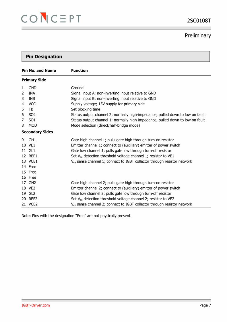
Pin Designation
Pin No. and Name Function
Primary Side
1 GND Ground 2 INA Signal input A; non-inverting input relative to GND 3 INB Signal input B; non-inverting input relative to GND 4 VCC Supply voltage; 15V supply for primary side 5 TB Set blocking time 6 SO2 Status output channel 2; normally high-impedance, pulled down to low on fault 7 SO1 Status output channel 1; normally high-impedance, pulled down to low on fault 8 MOD Mode selection (direct/half-bridge mode)
Secondary Sides
9 GH1 Gate high channel 1; pulls gate high through turn-on resistor 10 VE1 Emitter channel 1; connect to (auxiliary) emitter of power switch 11 GL1 Gate low channel 1; pulls gate low through turn-off resistor 12 REF1 Set Vce detection threshold voltage channel 1; resistor to VE1 13 14 15 16
VCE1 Free Free Free
Vce sense channel 1; connect to IGBT collector through resistor network
17 GH2 Gate high channel 2; pulls gate high through turn-on resistor 18 VE2 Emitter channel 2; connect to (auxiliary) emitter of power switch 19 GL2 Gate low channel 2; pulls gate low through turn-off resistor 20 REF2 Set Vce detection threshold voltage channel 2; resistor to VE2 21 VCE2 Vce sense channel 2; connect to IGBT collector through resistor network
Note: Pins with the designation “Free” are not physically present.

2SC0108T Description & Application Manual
Page 8 INTELLIGENT POWER ELECTRONICS
Recommended Interface Circuitry for the Primary Side Connector
2
8
4
3
1
5
6
7
Driver 2SC0108T
GND
INA
SO1
+3.3V...+15V
PWM 2
Fault 2
R1
INB
SO2
PWM 1
Fault 1
R2 TB
Rb
VCC+15V
GND
MOD
Rm
D1 D2
Cm
Fig. 5 Recommended user interface of 2SC0108T (primary side)
Description of Primary Side Interface
General
The primary side interface of the driver 2SC0108T is very simple and easy to use.
The driver primary side is equipped with an 8-pin interface connector with the following terminals:
• 1 x power-supply terminal • 2 x drive signal inputs • 2 x status outputs (fault returns) • 1 x mode selection input (half-bridge mode / direct mode) • 1 x input to set the blocking time
All inputs and outputs are ESD-protected. Moreover, all digital inputs have Schmitt-trigger characteristics.
VCC terminal
The driver has one VCC terminal on the interface connector. It supplies the primary side electronics as well as the DC-DC converter to supply the secondary sides with 15V.
The driver limits the inrush current at startup and no external current limitation of the voltage source for VCC is needed.

2SC0108T Preliminary
IGBT-Driver.com Page 9
MOD (mode selection)
The MOD input allows the operating mode to be selected with a resistor connected to GND.
Direct mode If the MOD input is connected to GND, direct mode is selected. In this mode, there is no interdependence between the two channels. Input INA directly influences channel 1 while INB influences channel 2. High level at an input (INA or INB) always results in turn-on of the corresponding IGBT. In a half-bridge topology, this mode should be selected only when the dead times are generated by the control circuitry so that each IGBT receives its own drive signal.
Caution: Synchronous or overlapping timing of both switches of a half-bridge basically shorts the DC link.
Half-bridge mode
If the MOD input is connected to GND with a resistor 71k<Rm<181k, half-bridge mode is selected. In this mode, the inputs INA and INB have the following functions: INA is the drive signal input while INB acts as the enable input (see Fig. 6). It is recommended to place a capacitor Cm=22nF in parallel to Rm in order to reduce the deviation between the dead times at the rising and falling edges of INA respectively.
When input INB is low level, both channels are blocked. If it goes high, both channels are enabled and follow the signal on the input INA. At the transition of INA from low to high, channel 2 turns off immediately and channel 1 turns on after a dead time Td.
0V
-8V
+15V
+3.3...15V
Gate G1
InA
-8V
+15VGate G2
0V+3.3...15V
Both channels OFF
Dead time (both channels OFF)
InB
Fig. 6 Signals in half-bridge mode
The value of the dead time Td is determined by the value of the resistor Rm according to the following formula (typical value):
4.56][33][ +⋅=Ω sTkR dm μ where 0.5μs<Td<3.8μs and 73kΩ<Rm<182kΩ

2SC0108T Description & Application Manual
Page 10 INTELLIGENT POWER ELECTRONICS
INA, INB (channel drive inputs, e.g. PWM)
INA and INB are basically drive inputs, but their function depends on the MOD input (see above). They safely recognize signals in the whole logic-level range between 3.3V and 15V. Both input terminals feature Schmitt-trigger characteristics (refer to the driver data sheet /3/). An input transition is triggered at any edge of an incoming signal at INA or INB.
SO1, SO2 (status outputs)
The outputs SOx have open-drain transistors. When no fault condition is detected, the outputs have high impedance. An internal current source of 500μA pulls the SOx outputs to a voltage of about 4V when leaved open. When a fault condition (primary side supply undervoltage, secondary side supply undervoltage, IGBT short-circuit or overcurrent) is detected, the corresponding status output SOx goes to low (connected to GND).
The diodes D1 and D2 must be Schottky diodes and must only be used when using 3.3V logic. For 5V…15V logic, they can be omitted.
The maximum SOx current in a fault condition must not exceed the value specified in the driver data sheet /3/.
Both SOx outputs can be connected together to provide a common fault signal (e.g. for one phase). However, it is recommended to evaluate the status signals individually to allow fast and precise fault diagnosis.
How the status information is processed
a) A fault on the secondary side (detection of short-circuit of IGBT module or supply undervoltage) is transmitted to the corresponding SOx output immediately. The SOx output is automatically reset (returning to a high impedance state) after a blocking time Tb has elapsed (refer to “TB (input for adjusting the blocking time Tb)” for timing information).
b) A supply undervoltage on the primary side is indicated to both SOx outputs at the same time. Both SOx outputs are automatically reset (returning to a high impedance state) when the undervoltage on the primary side disappears.
TB (input for adjusting the blocking time Tb)
The terminal TB allows the blocking time Tb to be set by connecting a resistor Rb to GND (see Fig. 5). The following equation calculates the value of Rb connected between pins TB and GND in order to program the desired blocking time Tb (typical value):
51][0.1][ +⋅=Ω msTkR bb where 20ms<Tb<130ms and 71kΩ<Rb<181kΩ
The blocking time can also be set to a minimum of 9µs (typical) by selecting Rb=0Ω. The terminal TB must not be left floating.
Note: It is also possible to apply a stabilized voltage at TB. The following equation is used to calculate the voltage Vb between TB and GND in order to program the desired blocking time Tb (typical value):
02.1][02.0][ +⋅= msTVV bb where 20ms<Tb<130ms and 1.42<Vb<3.62V

2SC0108T Preliminary
IGBT-Driver.com Page 11
Recommended Interface Circuitry for the Secondary Side Connectors
19
Driver
Rth2
REF2
VCE2
VE2
GH2
GL2
Rg,off2
Rg,on2
D12
Ra2
Gate 2
Collector 2
22k Ca2Emitter 2
2SC0108T
9
10
11
12
13
20
18
17
21
Rth1
REF1
VCE1
VE1
GH1
GL1
Rg,off1
Rg,on1
D11
Ra1
Gate 1
Collector 1
22k Ca1Emitter 1
Rvce1
Rvce2
D32
D52
D51
D31
D22
D21D41
D42
Fig. 7 Recommended user interface of 2SC0108T (secondary sides)
Description of Secondary Side Interfaces
General
Each driver’s secondary side (driver channel) is equipped with a 5-pin interface connector with the following terminals (x stands for the number of the drive channel 1 or 2):
• 1 x emitter terminal VEx • 1 x reference terminal REFx for overcurrent or short-circuit protection • 1 x collector sense terminal VCEx • 1 x turn-on gate terminal GHx • 1 x turn-off gate terminal GLx
All inputs and outputs are ESD-protected.
Emitter terminal (VEx)
The emitter terminal must be connected to the IGBT auxiliary emitter with the circuit shown in Fig. 7.

2SC0108T Description & Application Manual
Page 12 INTELLIGENT POWER ELECTRONICS
Reference terminals (REFx)
The reference terminal REFx allows the threshold to be set for short-circuit and/or overcurrent protection with a resistor placed between REFx and VEx. A constant current of 150µA is provided at pin REFx.
Collector sense (VCEx) with resistors
The collector sense of each channel of the 2SC0108T must be connected to the IGBT collector or MOSFET drain with the circuit shown in Figs. 7 or 8 in order to detect an IGBT or MOSFET overcurrent or short-circuit.
In an IGBT off-state, the driver’s internal MOSFET connects pin VCEx to pin COMx. The capacitor Cax is then precharged/discharged to the negative supply voltage, which is about -8V referred to VEx (red circle in Fig. 8 left). During this time, a current flows from the collector (blue circle in Fig. 8) via the resistor network and the diode BAS416 to GHx. The current is limited by the resistor chain.
It is recommended to dimension the resistor value of Rvcex in order to obtain a current of about IRvcex=0.6-1mA flowing through Rvcex (e.g. 1.2-1.8MΩ for VDC-LINK=1200V). The current through Rvcex must not exceed 1mA. A high-voltage resistor as well as series-connected resistors may be used. In any case, the minimum creepage distance required for the application must be considered.
The reference voltage is set by the resistor Rthx. It is calculated from the reference current (typically 150uA) and the reference resistance Rthx (green circle in Fig. 8)
thxrefx RAV ⋅= μ150
CONCEPT recommends the use of Rthx=68kΩ. In this case the driver will safely protect the IGBT against short-circuit, but not necessarily against overcurrent. Overcurrent protection has a lower timing priority and is recommended to be realized within the host controller. Lower resistance values make the system more sensitive and do not provide any advantages in the case of desaturated IGBTs (short-circuit).
GLx
VEx
2SC0108T (Part of One Channel Shown)
Rg(on)
Rg(off)GHx
Vce Monitoring
VCEx
VISOx
REFx
+
-
Rthx
Rax
Cax
RvcexBAS416
0.6...1mA
150uA
Vrefx
Vce sat
COMx
VCEx
t (us)
Gate-Emitter
Fault
22k
COMx
Voltage
Fig. 8 Vce desaturation protection with resistors
At IGBT turn-on and in the on-state, the driver’s internal MOSFET turns off. While Vce decreases (blue curve in Fig. 8), Cax is charged from the COMx potential to the IGBT saturation voltage (red curve in Fig. 8). The time required to charge Cax depends on the DC bus voltage, the value of the resistor Rax and the value of the capacitor Cax. For 1200V and 1700V IGBTs it is recommended to set Rax=120kΩ. For 600V IGBTs the recommended value is Rax=62kΩ.
During the response time, the Vce monitoring circuit is inactive. The response time is the time that elapses after turn-on of the power semiconductor until the collector voltage is measured. It corresponds to the short-circuit duration.

2SC0108T Preliminary
IGBT-Driver.com Page 13
The value of the response time capacitors Cax can be determined from the following table in order to set the desired response time (Rvcex=1.8MΩ, Rax=120kΩ, DC-link voltage VDC-LINK>550V):
Cax [pF] Rthx [kΩ]/Vthx [V] Response time [μs]
0 43 / 6.45 1.2
15 43 / 6.45 3.2
22 43 / 6.45 4.2
33 43 / 6.45 5.8
47 43 / 6.45 7.8
0 68 / 10.2 1.5
15 68 / 10.2 4.9
22 68 / 10.2 6.5
33 68 / 10.2 8.9
47 68 / 10.2 12.2
Table 1 Typical response time as a function of the capacitance Cax and the resistance Rthx
As the parasitic capacitances on the host PCB may influence the response time, it is recommended to measure it in the final design. It is important to define a response time which is shorter than the maximum permitted short-circuit duration of the power semiconductor used.
Note that the response time increases at DC-link voltage values lower than 550V (Rax=120kΩ) and/or higher threshold voltage values Vthx. The response time will decrease at lower threshold voltage values.
The diode D1x in Fig. 7 must have a very low leakage current and a blocking voltage >40V (e.g. BAS416). Schottky diodes must be explicitly avoided.
The components Cax, Rax, Rthx and D1x must be placed as close as possible to the driver. A large collector-emitter loop must also be avoided. See the proposed layout of 2BB0108T on www.igbt-driver.com/go/2BB0108T
When a short-circuit/overcurrent fault is detected, the driver switches off the corresponding power semiconductor. The fault status is immediately transferred to the corresponding SOx output of the affected channel. The power semiconductor is kept in the off state (non-conducting) and the fault is shown at pin SOx as long as the blocking time Tb is active.
The blocking time Tb is applied independently to each channel. Tb starts as soon as a fault has been detected.
Desaturation protection with sense diodes
2SC0108T also provides desaturation protection with high-voltage diodes as shown in Fig. 9. However, the use of high-voltage diodes has some disadvantages compared to the use of resistors:
• Common-mode current relating to the rate of change dvce/dt of the collector-emitter voltage: High-voltage diodes have large junction capacitances Cj. These capacitances in combination with the dvce/dt generate a common-mode current Icom flowing in and out of the measurement circuit.
dtdvCI ce
jcom ⋅=
• Price: High-voltage diodes are more expensive than standard 0805/150V or 1206/200V SMD resistors.
• Availability: Standard thick-film resistors are comparatively easier to source on the market.

2SC0108T Description & Application Manual
Page 14 INTELLIGENT POWER ELECTRONICS
• Limited ruggedness: The reaction time does not increase at lower Vce levels. Consequently, false triggering may occur at higher IGBT temperatures, higher collector currents, resonant switching or phase-shift PWM, particularly when the reference voltage Vthx is set below about 10V. The upper limit of the reference voltage is restricted to about 10V, which may lead to limited IGBT utilization: the collector current may be limited to values smaller than twice the nominal current, or the short-circuit withstand capability may be reduced.
During the IGBT off-state, D4x (and Rax) sets the VCEx pin to COMx potential, thereby precharging/discharging the capacitor Cax to the negative supply voltage, which is about -8V referred to VEx. At IGBT turn-on, the capacitor Cax is charged via Rax. When the IGBT collector-emitter voltage drops below that limit, the voltage of Cax is limited via the high-voltage diodes D1x and D2x. The voltage across Cax can be calculated by:
))330(
)15(330( )2()1(
)2()1( Ω+−−−
⋅Ω+++=ax
xDFxDFCEsatxDFxDFCEsatCax R
VVVVVVVV
The reference voltage Vrefx must be higher than Vcax. The reference voltage is set up by the resistor Rthx. The reference voltage is calculated via the reference current (typically 150uA) and the reference resistance Rthx:
thxrefx RAV ⋅= μ150
Collector
2SC0108T
330
Rax
Cax15k
D1xVCEx
Gate or GHx
VEx
D2x
VEx
D4x
D3x
Fig. 9 Recommended circuit for desaturation protection with sense diodes (one channel shown)
The value of the resistance Rax can be calculated with the following equation in order to program the desired response time Tax at turn-on:
)1515
ln(][
][1000≈][
refx
GLxax
axax
VVVV
pFC
sTkR
−+
⋅
⋅Ω
μ Eq. 6
VGLx is the absolute value of the turn-off voltage at the driver output. It depends on the driver load and can be found in the driver data sheet /3/.
Recommended components D1x/D2x/D3x/D4x and values for Rax and Cax are:
• High-voltage diodes D1x/D2x: 2x 1N4007 for 1200V IGBT 3x 1N4007 for 1700V IGBT
• D3x: Transient voltage suppressor of the voltage class 12V…15V with small junction capacitance as CDDFN2-12C from Bourns.
• D4x: High-speed diode as BAS316. Schottky diodes must be avoided.
• Rax=24kΩ…62kΩ
• Cax=100pF…560pF
Note that Cax must include the parasitic capacitance of the transient voltage suppressor D3x and the PCB.

2SC0108T Preliminary
IGBT-Driver.com Page 15
Note also that the instantaneous Vce threshold voltage is determined by the voltage at pin REFx (150μA through Rthx) minus the voltage across the 330Ω resistor as well as the forward voltages across D1x and D2x.
The minimum off-state duration should not be shorter than about 1µs in order not to significantly reduce the response time for the next turn-on pulse.
Example: A resistor of Rax≈46kΩ must be used to define a response time of 6μs with Cax=150pF, Rthx=33kΩ and VGLx=9V.
Disabling the Vce,sat detection
To disable the Vce,sat measurement of 2SC0108T, a resistor with a minimum value of 33kΩ must be placed between VCEx and VEx according to Fig. 10.
The reference resistor Rthx may be chosen between 33kΩ and infinity, i.e. the REFx pin may be left open.
19
Driver
Rth2
REF2
VCE2
VE2
GH2
GL2
Rg,off2
Rg,on2
Gate 2
22kEmitter 2
2SC0108T
9
10
11
12
13
20
18
17
21
Rth1
REF1
VCE1
VE1
GH1
GL1
Rg,off1
Rg,on1
Gate 1
22kEmitter 1
33k
33k
Fig. 10 Disabling the Vce,sat detection
Gate turn-on (GHx) and turn-off (GLx) terminals
These terminals allow the turn-on (GHx) and turn-off (GLx) gate resistors to be connected to the gate of the power semiconductor. The GHx and GLx pins are available as separated terminals in order to set the turn-on and turn-off resistors independently without the use of an additional diode. Please refer to the driver data sheet /3/ for the limit values of the gate resistors used.
A resistor between GLx and VEx of 22k (higher values are also possible) may be used in order to provide a low-impedance path from the IGBT gate to the emitter even if the driver is not supplied with power. Lower resistance values are not allowed.
A transient voltage suppressor device (D5x) may be used between gate and emitter (e.g. SMBJ13CA) if the gate-emitter voltage becomes too high in the IGBT short-circuit condition, thus leading to excessive short-circuit currents.
Note however that it is not advisable to operate the power semiconductors within a half-bridge with a driver in the event of a low supply voltage. Otherwise, a high rate of increase of Vce may cause partial turn-on of these IGBTs.

2SC0108T Description & Application Manual
Page 16 INTELLIGENT POWER ELECTRONICS
Active clamping
Active clamping is a technique designed to partially turn on the power semiconductor as soon as the collector-emitter (drain-source) voltage exceeds a predefined threshold. The power semiconductor is then kept in linear operation.
Basic active clamping topologies implement a single feedback path from the IGBT’s collector through transient voltage suppressor devices (TVS) to the IGBT gate. The 2SC0108T supports basic active clamping.
It is recommended to use the circuit shown in Fig. 7. The following parameters must be adapted to the application:
• TVS D2x, D3x and D4x. It is recommended to use:
- Six 80V TVS with 600V IGBTs with DC link voltages up to 430V. Good clamping results can be obtained with five unidirectional TVS P6SMBJ70A and one bidirectional TVS P6SMBJ70CA from Semikron or with five unidirectional TVS SMBJ70A-E3 and one bidirectional TVS SMBJ70CA-E3 from Vishay.
- Six 150V TVS with 1200V IGBTs with DC link voltages up to 800V. Good clamping results can be obtained with five unidirectional TVS SMBJ130A-E3 and one bidirectional TVS SMBJ130CA-E3 from Vishay or five unidirectional TVS SMBJ130A-TR from ST and one bidirectional TVS P6SMBJ130CA from Diotec.
- Six 220V TVS with 1700V IGBTs with DC link voltages up to 1200V. Good clamping results can be obtained with five unidirectional TVS P6SMB220A and one bidirectional TVS P6SMB220CA from Diotec or five unidirectional TVS SMBJ188A-E3 and one bidirectional TVS SMBJ188CA-E3 from Vishay.
At least one bidirectional TVS (D2x) per channel must be used in order to avoid negative current flowing through the TVS chain during turn-on of the antiparallel diode of the IGBT module due to its forward recovery behavior. Such a current could, depending on the application, lead to undervoltage of the driver secondary voltage VISOx to VEx (15V).
Note that it is possible to modify the number of TVS in a chain. The active clamping efficiency can be improved by increasing the number of TVS used in a chain if the total threshold voltage remains at the same value. Note also that the active clamping efficiency is highly dependent on the type of TVS used (e.g. manufacturer).
Note that the active clamping performance can be improved by increasing the value of the turn-off gate resistors Rg,offx.
If active clamping is not used, the TVS D2x, D3x and D4x can be omitted.
How Do 2SC0108T SCALE-2 Drivers Work in Detail?
Power supply and electrical isolation
The driver is equipped with a DC/DC converter to provide an electrically insulated power supply to the gate driver circuitry. All transformers (DC/DC and signal transformers) feature safe isolation to EN 50178, protection class II between primary side and either secondary side.
Note that the driver requires a stabilized supply voltage.

2SC0108T Preliminary
IGBT-Driver.com Page 17
Power-supply monitoring
The driver’s primary side as well as both secondary-side driver channels are equipped with a local undervoltage monitoring circuit.
In the event of a primary-side supply undervoltage, the power semiconductors are driven with a negative gate voltage to keep them in the off-state (the driver is blocked) and the fault is transmitted to both outputs SO1 and SO2 until the fault disappears.
In case of a secondary-side supply undervoltage, the corresponding power semiconductor is driven with a negative gate voltage to keep it in the off-state (the channel is blocked) and a fault condition is transmitted to the corresponding SOx output. The SOx output is automatically reset (returning to a high impedance state) after the blocking time.
Within a half-bridge, it is advised not to operate the IGBTs with an IGBT driver in the event of a low supply voltage. Otherwise, a high rate of increase of Vce may cause partial turn-on of these IGBTs.
Parallel connection of 2SC0108T
If parallel connection of 2SC0108T drivers is required, please refer to the application note AN-0904 /5/ on www.IGBT-Driver.com/go/app-note.
3-level or multilevel topologies
If 2SC0108T drivers are to be used in 3-level or multilevel topologies, please refer to the application note AN-0901 /6/ on www.IGBT-Driver.com/go/app-note.
Additional application support for 2SC0108T
For additional application support using 2SC0108T drivers, please refer to the application note AN-1101 /4/ on www.IGBT-Driver.com/go/app-note.
Bibliography
/1/ “Smart Power Chip Tuning”, Bodo’s Power Systems, May 2007
/2/ “Description and Application Manual for SCALE Drivers”, CONCEPT
/3/ Data sheet SCALE-2 driver core 2SC0108T, CONCEPT
/4/ Application note AN-1101: Application with SCALE-2 Gate Driver Cores, CONCEPT
/5/ Application note AN-0904: Direct Paralleling of SCALE-2 Gate Driver Cores, CONCEPT
/6/ Application note AN-0901: Methodology for Controlling Multi-Level Converter Topologies with SCALE-2 IGBT Drivers, CONCEPT
Note: These papers are available on the Internet at www.IGBT-Driver.com/go/papers
2SC0108T Description & Application Manual
Page 18 INTELLIGENT POWER ELECTRONICS
The Information Source: SCALE-2 Driver Data Sheets
CONCEPT offers the widest selection of gate drivers for power MOSFETs and IGBTs for almost any application requirements. The largest website on gate-drive circuitry anywhere contains all data sheets, application notes and manuals, technical information and support sections: www.IGBT-Driver.com
Quite Special: Customized SCALE-2 Drivers
If you need an IGBT driver that is not included in the delivery range, please don’t hesitate to contact CONCEPT or your CONCEPT sales partner.
CONCEPT has more than 20 years experience in the development and manufacture of intelligent gate drivers for power MOSFETs and IGBTs and has already implemented a large number of customized solutions.
Technical Support
CONCEPT provides expert help with your questions and problems:
www.IGBT-Driver.com/go/support
Quality
The obligation to high quality is one of the central features laid down in the mission statement of CT-Concept Technologie AG. The quality management system covers all stages of product development and production up to delivery. The drivers of the SCALE-2 series are manufactured to the ISO9001:2000 quality standard.
Legal Disclaimer
This data sheet specifies devices but cannot promise to deliver any specific characteristics. No warranty or guarantee is given – either expressly or implicitly – regarding delivery, performance or suitability.
CT-Concept Technologie AG reserves the right to make modifications to its technical data and product specifications at any time without prior notice. The general terms and conditions of delivery of CT-Concept Technologie AG apply.

2SC0108T Preliminary
IGBT-Driver.com Page 19
Ordering Information
The general terms and conditions of delivery of CT-Concept Technologie AG apply.
Type Designation Description
2SC0108T2A0-17 Dual-channel SCALE-2 driver core (standard version, -20°C…85°C) 2SC0108T2B0-17 Dual-channel SCALE-2 driver core (-40°C…85°C) 2SC0108T2C0-17 Dual-channel SCALE-2 driver core (-40°C…85°C, connector pin length:
5.84mm) Product home page: www.IGBT-Driver.com/go/2SC0108T Refer to www.IGBT-Driver.com/go/nomenclature for information on driver nomenclature
Information about Other Products
For other driver cores:
Direct link: www.IGBT-Driver.com/go/cores
For other drivers, product documentation, evaluation systems and application support
Please click onto: www.IGBT-Driver.com
Manufacturer
CT-Concept Technologie AG Intelligent Power Electronics Renferstrasse 15 CH-2504 Biel-Bienne Switzerland Tel. +41 - 32 - 344 47 47 Fax +41 - 32 - 344 47 40 E-mail [email protected] Internet www.IGBT-Driver.com © 2009…2011 CT-Concept Technologie AG - Switzerland. All rights reserved. We reserve the right to make any technical modifications without prior notice. Version of 2011-09-09