2d materials: properties, applications and synthesis methods · $17.8m national user facility to...
TRANSCRIPT

2D Materials: Properties, Applications and Synthesis Methods
Joan Redwing 4/14/2016

Where is Penn State?
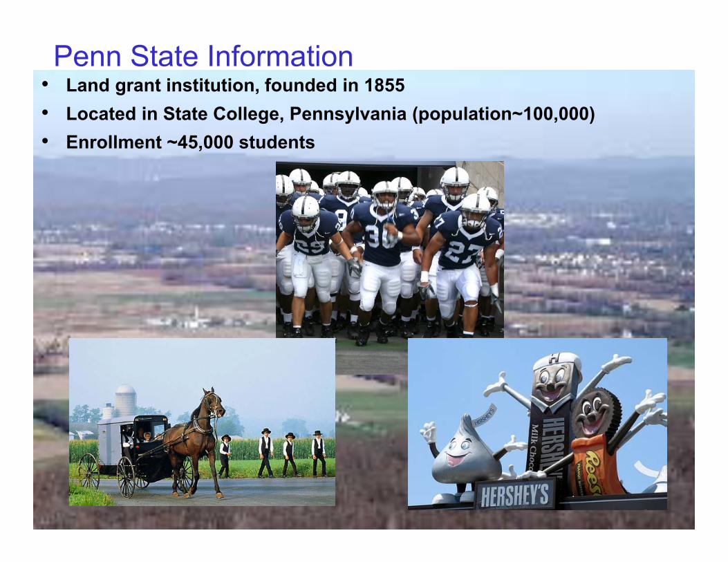
Penn State Information• Land grant institution, founded in 1855• Located in State College, Pennsylvania (population~100,000)• Enrollment ~45,000 students

Materials Research at Penn State
• 200+ faculty, 800+ grad students, 15 academic departments
• Materials Research Institute• Millennium Science Complex
• Huck Institute for Life Sciences and Materials Research Institute
• Nanofabrication Facility (part of National Nanofabrication Infrastructure Network)
• Materials Characterization Facility
Millennium Science Complex

Electronic Materials SynthesisOur research is focused on the development of new processes, materials and device structures using chemical vapor deposition-based techniques.
Thin Films
Substrate
Silicon nanowires
GaNAlNSiC
Nanoscale Materials
Substrate Substrate
2D Layered Materials
Process Chemistry ↔ Material Structure ↔ Properties ↔ Device Applications

$17.8M national user facility to advance synthesis of 2D materials for next generation electronics
2D chalcogenide monolayers, surfaces and interfaces are emerging as a compelling class of systems with transformative new science that can be harnessed for novel device technologies in next-generation electronics.
An NSF user facility with broad access:
Hybrid MBEChalcogenide MOCVD
CVT, Bridgman
STM/AFMARPES4-probe
Raman, PL
DFTReactive FFMonte CarloPhase field
insights into growthin situ measurement
characterization & interpretation
• Open calls for user proposals,• No user fees for academic use• Access to a team of local experts • Community knowledge-base of synthetic
protocols
• Webinars, Workshops, Website resources• Partnership opportunities with PUI, MSI
mip.psu.edu
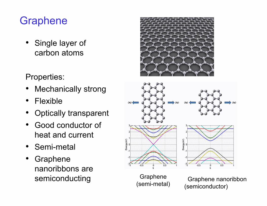
Graphene
• Single layer of carbon atoms
Properties:• Mechanically strong• Flexible• Optically transparent• Good conductor of
heat and current• Semi-metal• Graphene
nanoribbons are semiconducting Graphene
(semi-metal)Graphene nanoribbon
(semiconductor)
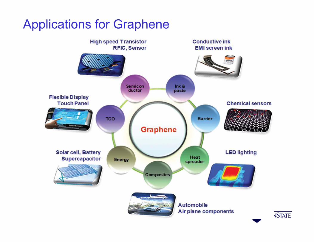
Applications for Graphene
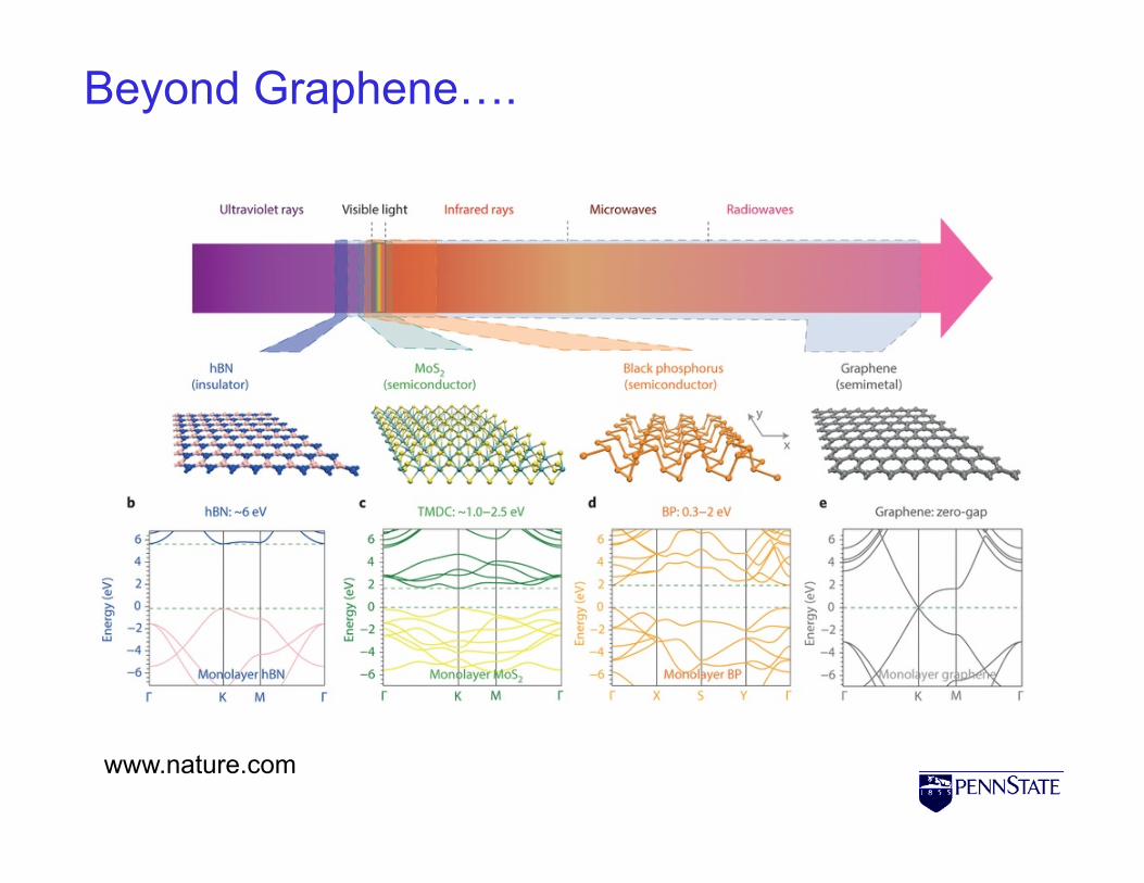
Beyond Graphene….
www.nature.com

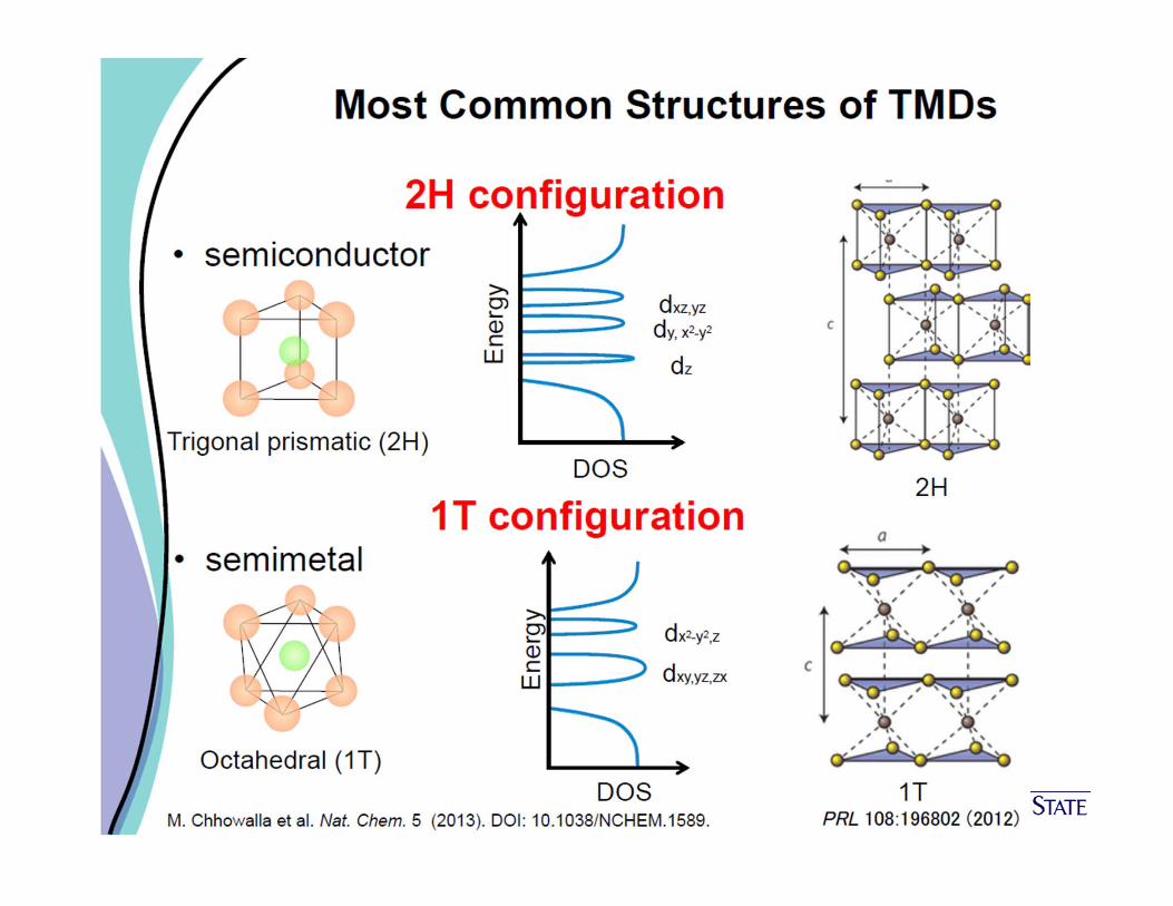
2D Chalcogenides
Q.H. Huang, et al. Nature Nanotech. 7 (2012) p. 699
A.K. Geim and I.V. GrigorievaNature 499 (2013) p. 419
• Graphene-like layered materials• Exhibit wide variety of electronic
properties – insulators, semiconductors, metals, superconductors
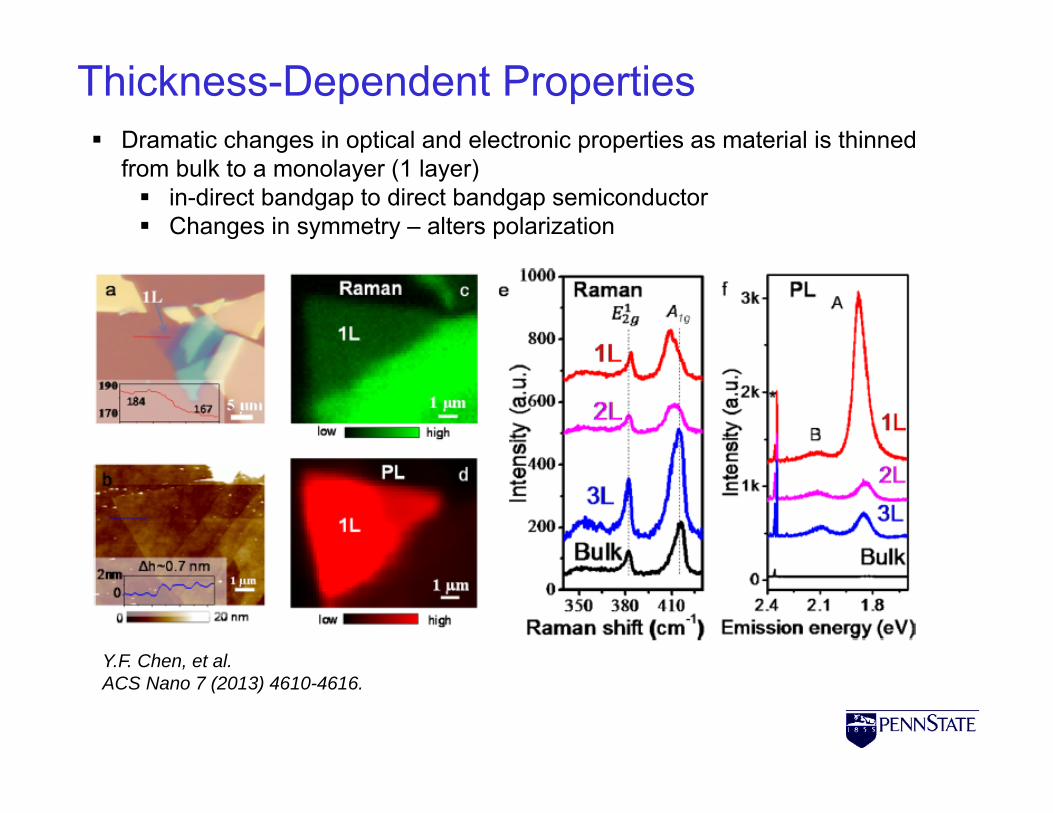
Thickness-Dependent Properties Dramatic changes in optical and electronic properties as material is thinned
from bulk to a monolayer (1 layer) in-direct bandgap to direct bandgap semiconductor Changes in symmetry – alters polarization
K.F. Mak, et al.Phys. Rev. Lett 105 (2010) 136805.
Y.F. Chen, et al.ACS Nano 7 (2013) 4610-4616.

2D Heterostructures
A.K. Geim and I.V. GrigorievaNature 499 (2013) p. 419
Van der Waals bonding enables stacking of different materials without need to form chemical bonds

2D Electronics
Q.H. Huang, et al. Nature Nanotech. 7 (2012) p. 699 Transistors made of atomically thin
layers (good for electrostatics)
Transfer of 2D layers onto plastic substrates for flexible electronics

Paper Discussion #1
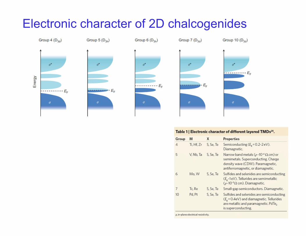
Electronic character of 2D chalcogenides

Band alignment of layered chalcogenides
APPLIED PHYSICS LETTERS 103, 053513 (2013)


Bulk 2D chalcogenides (MoS2 example)• Naturally occurring in molybdenite ore
• Powder used in lubricants
• Bulk synthesis methods (for higher purity material):• Sulfurization of MoO3 powder (Heat in H2S, etc.)• Chemical vapor transport
Manchester Nanocrystals
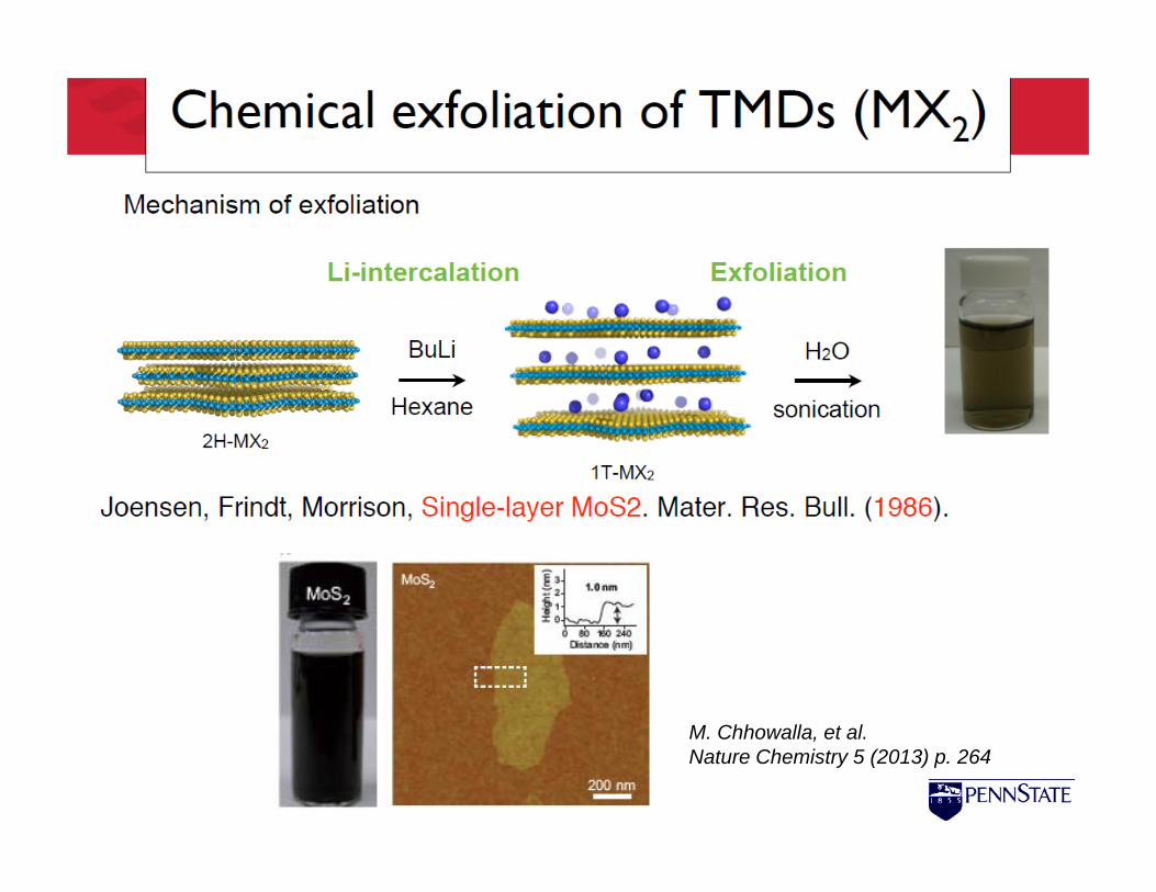
M. Chhowalla, et al. Nature Chemistry 5 (2013) p. 264

Metal transformation

Powder vapor transport(also referred to as chemical vapor deposition)
M. Chhowalla, et al. Nature Chemistry 5 (2013) p. 264
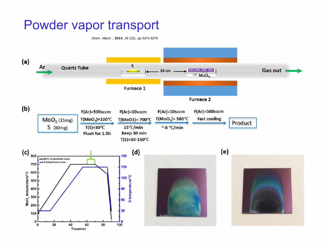
Powder vapor transportChem. Mater., 2014, 26 (22), pp 6371–6379
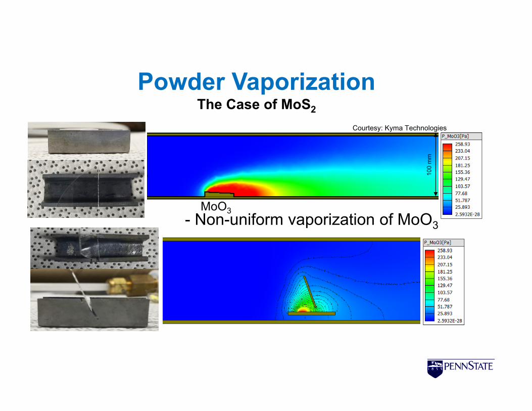
MoO3
Courtesy: Kyma Technologies
100
mm
- Non-uniform vaporization of MoO3
Powder VaporizationThe Case of MoS2

Powder Vapor Transport
Nature Materials, doi:10.1038/nmat4064 (2014)
Nature Materials 13, 1135–1142 (2014)
WS2-WSe2 lateral heterostructures
MoS2-MoSe2 lateral heterostructures
Nature Nanotechnology 9, 1024–1030 (2014)
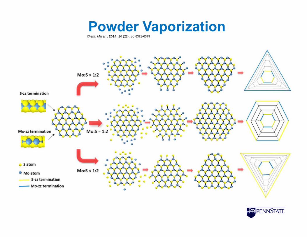
Powder VaporizationChem. Mater., 2014, 26 (22), pp 6371–6379

Point defects
NATURE COMMUNICATIONS | DOI: 10.1038/ncomms7293

Chemical Vapor Deposition
Advantages: Scalable to large substrate diameters Offers good control over deposition
rate Can easily change precursors for
growth of heterostructures
Deposition occurs via chemical reaction of precursor molecules
Variety of precursors: Mo(CO)6, MoCl5 W(CO)6, WF6 H2Se, (CH3)2Se, SeCl4 H2S, (C2H5)2S
Challenges: Mo, W, etc. high melting points
(>2000oC)/low vapor pressure S, Se, etc. low melting points
(<250oC)/high vapor pressure
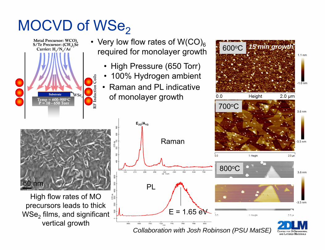
MOCVD of WSe2
50 nm
High flow rates of MO precursors leads to thick
WSe2 films, and significant vertical growth
• Very low flow rates of W(CO)6required for monolayer growth
700oC
800oC
E2G/A1G
Raman
PL
E = 1.65 eV
• Raman and PL indicative of monolayer growth
600oC
• High Pressure (650 Torr)• 100% Hydrogen ambient
15 min growth
Collaboration with Josh Robinson (PSU MatSE)

MOCVD of WSe2
Mapping region
Normalized Raman Normalized PL
E12g
Raman Mapping PL Mapping 1.60 eV
Growth Conditions: W(CO)6, (CH3)2Se, H2 carrier gas 800oC, 700 Torr W(CO)6=3.3x10⁻⁴ sccm, Se/W=2.4x105
c-plane (0001) sapphire
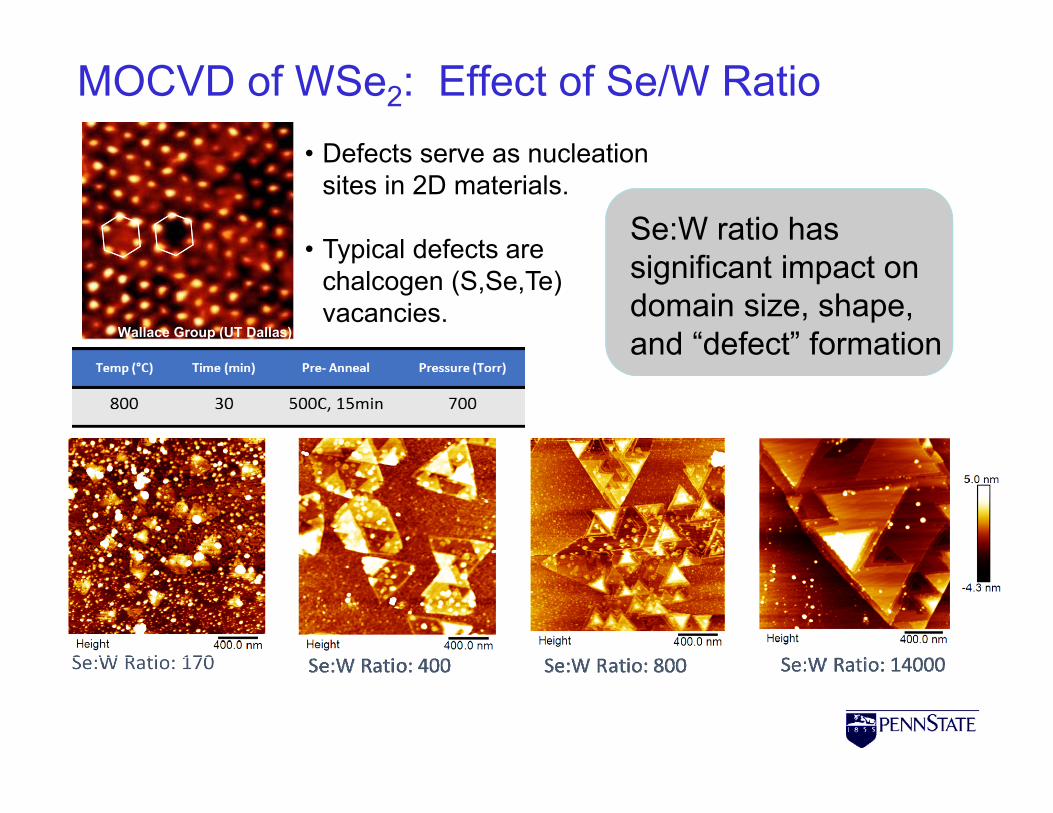
MOCVD of WSe2: Effect of Se/W Ratio• Defects serve as nucleation
sites in 2D materials.
• Typical defects are chalcogen (S,Se,Te) vacancies.
Wallace Group (UT Dallas)
Se:W ratio has significant impact on domain size, shape, and “defect” formation

WSe2 on Free Standing Graphene Templates
After MOCVD Growth
As Prepared
A. Azizi, et al. ACS Nano (in press)
Nasim Alem, Josh Robinson
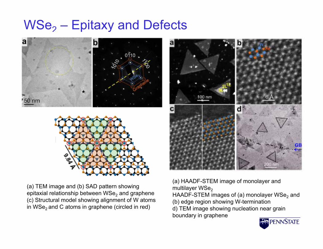
WSe2 – Epitaxy and Defects
(a) HAADF-STEM image of monolayer and multilayer WSe2HAADF-STEM images of (a) monolayer WSe2 and (b) edge region showing W-terminationd) TEM image showing nucleation near grain boundary in graphene
(a) TEM image and (b) SAD pattern showing epitaxial relationship between WSe2 and graphene(c) Structural model showing alignment of W atoms in WSe2 and C atoms in graphene (circled in red)

to=26 hours

Paper Discussion #2
https://search.yahoo.com/yhs/search?p=nokia+morph+video&ei=UTF-8&hspart=moz
Watch Nokia Morph video:

What properties are important for flexible electronics?

Why 2D materials?

Properties of selected 2D materials
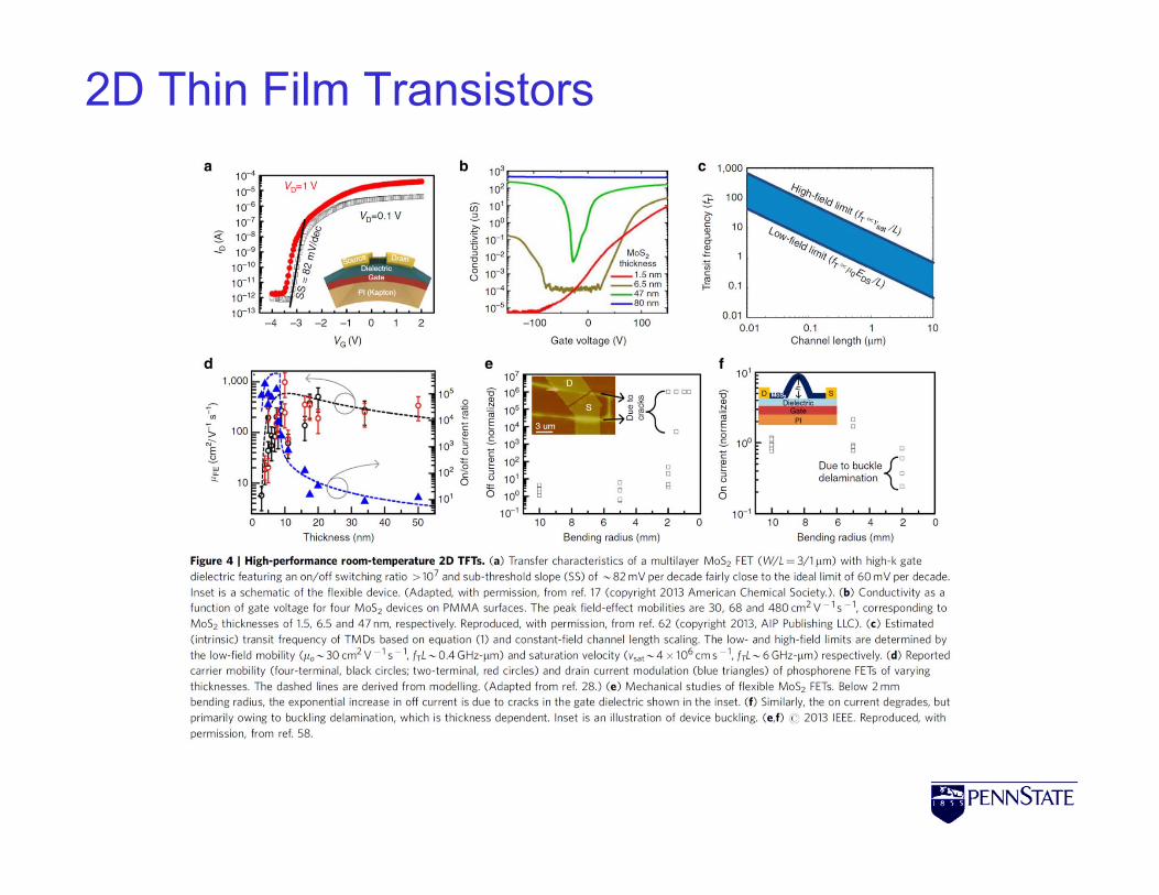
2D Thin Film Transistors

Heterostructure devices

Roll-to-roll manufacturing