26.5w ac/dc isolated flyback converter design - allgpc.com · aa24070l (mps3) 5.6va clamp forward...
TRANSCRIPT

26.5W AC/DC Isolated Flyback Converter Design
by 斜阳古道:http://bbs.21dianyuan.com/thread-1764-1-1.htmlEric Wen 注:[email protected] 2016-12-01 V1

AA24070L (MPS3) 5.6VA Clamp Forward Power Rail
TASK : 26.5W 9-Outputs AC/DC Isolated Flyback Converter Design
SPECIFICATION : Technical Specification on Sept 10, 2008
DATE : 15 Sept. 2008
AA24070L (MPS3) 5.6VA Clamp Forward Power Rail
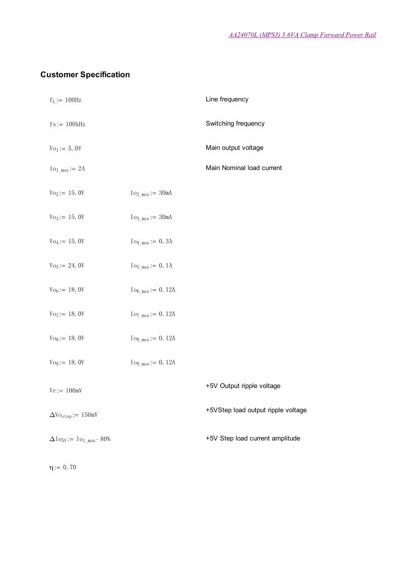
Customer Specification
fL 100Hz:= Line frequency
fs 100kHz:= Switching frequency
Vo1 5.0V:= Main output voltage
Io1_max 2A:= Main Nominal load current
Vo2 15.0V:= Io2_max 30mA:=
Vo3 15.0V:= Io3_max 30mA:=
Vo4 15.0V:= Io4_max 0.3A:=
Vo5 24.0V:= Io5_max 0.1A:=
Vo6 18.0V:= Io6_max 0.12A:=
Vo7 18.0V:= Io7_max 0.12A:=
Vo8 18.0V:= Io8_max 0.12A:=
Vo9 18.0V:= Io9_max 0.12A:=
+5V Output ripple voltageVr 100mV:=
+5VStep load output ripple voltageΔVostep 150mV:=
ΔIo5V Io1_max 80 %:= +5V Step load current amplitude
η 0.70:=

AA24070L (MPS3) 5.6VA Clamp Forward Power Rail
Definition Of Symbols
u t( ) Φ t( ):= Unit step function
mΩ 103- Ω:= Milliohm
ms 103-s:= Millisecond
μs 106-s:= Microsecond
ns 109-s:= Nanosecond
mW 103-W:= Milliwatts
mJ 103-J:= Millijoule
μJ 106-J:= Microjoule
nC 109-C:= Nanocoulomb
μm 106-m:= Micrometer
μo 4 π 107-
H m1-
:= Permeability of free space
ρ θ( ) 1.724 1 0.0042 θ 20-( )+[ ] 106- Ω cm:= Resistivity of copper at q degC
AA24070L (MPS3) 5.6VA Clamp Forward Power Rail
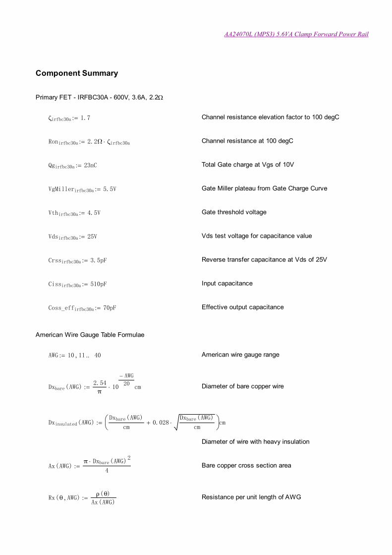
Component Summary
Primary FET - IRFBC30A - 600V, 3.6A, 2.2W
ζirfbc30a 1.7:= Channel resistance elevation factor to 100 degC
Ronirfbc30a 2.2Ω ζirfbc30a:= Channel resistance at 100 degC
Qgirfbc30a 23nC:= Total Gate charge at Vgs of 10V
VgMillerirfbc30a 5.5V:= Gate Miller plateau from Gate Charge Curve
Vthirfbc30a 4.5V:= Gate threshold voltage
Vdsirfbc30a 25V:= Vds test voltage for capacitance value
Crssirfbc30a 3.5pF:= Reverse transfer capacitance at Vds of 25V
Cissirfbc30a 510pF:= Input capacitance
Coss_effirfbc30a 70pF:= Effective output capacitance
American Wire Gauge Table Formulae
AWG 10 11, 40..:= American wire gauge range
Dxbare AWG( )2.54
π10
AWG-
20 cm:= Diameter of bare copper wire
Dxinsulated AWG( )Dxbare AWG( )
cm0.028
Dxbare AWG( )
cm+
cm:=
Diameter of wire with heavy insulation
Ax AWG( )π Dxbare AWG( )
2
4:= Bare copper cross section area
Rx θ AWG, ( )ρ θ( )
Ax AWG( ):= Resistance per unit length of AWG

AA24070L (MPS3) 5.6VA Clamp Forward Power Rail
Converter Parameters
Ts1
fs:= Converter period
Vgnom 220V:= Nominal input voltage
Vgmin Vgnom 1 20%-( ):= Minimum input voltage
Vgmin 176V=
Vgmax Vgnom 1 20%+( ):= Maximum input voltage
Vgmax 264V=
Pout1 Vo1 Io1_max Vo2 Io2_max+ Vo3 Io3_max+:=
Pout2 Vo4 Io4_max Vo5 Io5_max+:=
Pout3 Vo6 Io6_max Vo7 Io7_max+ Vo8 Io8_max+ Vo9 Io9_max+:=
Pout Pout1 Pout2+ Pout3+:=
Pout 26.44W=
AA24070L (MPS3) 5.6VA Clamp Forward Power Rail
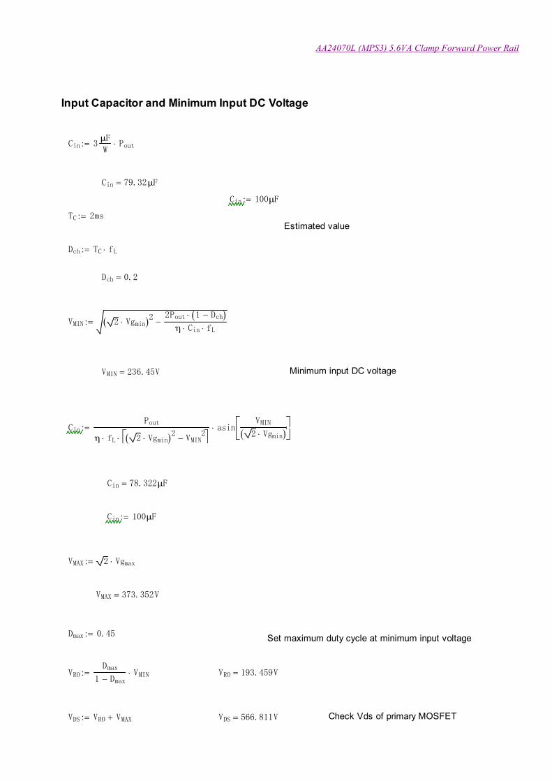
Input Capacitor and Minimum Input DC Voltage
Cin 3μFW
Pout:=
Cin 79.32μF=
Cin 100μF:=
TC 2ms:=Estimated value
Dch TC fL:=
Dch 0.2=
VMIN 2 Vgmin( )22Pout 1 Dch-( )
η Cin fL-:=
VMIN 236.45V= Minimum input DC voltage
CinPout
η fL 2 Vgmin( )2 VMIN2
- asin
VMIN
2 Vgmin( )
:=
Cin 78.322μF=
Cin 100μF:=
VMAX 2 Vgmax:=
VMAX 373.352V=
Dmax 0.45:=Set maximum duty cycle at minimum input voltage
VRODmax
1 Dmax-VMIN:= VRO 193.459V=
VDS VRO VMAX+:= VDS 566.811V= Check Vds of primary MOSFET
AA24070L (MPS3) 5.6VA Clamp Forward Power Rail
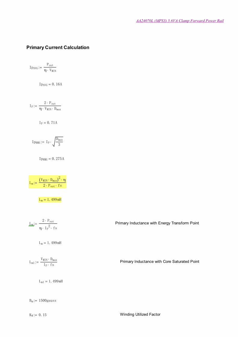
Primary Current Calculation
IpAVGPout
η VMIN:=
IpAVG 0.16A=
IP2 Pout
η VMIN Dmax:=
IP 0.71A=
IpRMS IPDmax
3:=
IpRMS 0.275A=
LmVMIN Dmax( )2 η
2 Pout fs:=
Lm 1.499mH=
Lm2 Pout
η IP2
fs:= Primary Inductance with Energy Transform Point
Lm 1.499mH=
Lm1VMIN Dmax
IP fs:= Primary Inductance with Core Saturated Point
Lm1 1.499mH=
Bm 1500gauss:=
KW 0.15:= Winding Utilized Factor

AA24070L (MPS3) 5.6VA Clamp Forward Power Rail
KJ 5 A mm2-
:=
APLm1 IP
2
Bm KW KJ cm4
1.14
cm4
:= AP22 Pout
η Bm3
Dmax fs
KW
2 KJ
:=
AP 0.635cm4
= AP2 0.52cm4
=
AP31.6 Pout
η Bm fs KW KJ cm4
1.14
cm4
:=AP4
Lm IP IpRMS
Bm KW KJ:=
AP3 0.492cm4
= AP4 0.26cm4
=
Power Transformer - EER28L/PC40 from TDK
AeEER35 107mm2
:= Effective cross section area
AwEER35 152.7mm2
:= Winding area base on BEER35-1112CPFR standardbobbin
APEER35 AeEER35 AwEER35:=
APEER35 1.634cm4
=
WtEER35 52g:=
AeEE35 89.3mm2
:= Effective cross section area
AwEE35 88.7mm2
:= Winding area base on BEE35-1112CPLFR standard bobbin
APEE35 AeEE35 AwEE35:=
APEE35 0.792cm4
=
:=

AA24070L (MPS3) 5.6VA Clamp Forward Power Rail
WtEE35 57g:=
AeEE32 83.2mm2
:= Effective cross section area
AwEE32 88.8mm2
:= Winding area base on BEE33-1112CPLFR standard bobbin
APEE32 AeEE32 AwEE32:=
APEE32 0.739cm4
=
WtEE32 32g:=
AeEE30 109mm2
:= Effective cross section area
AwEE30 44.5mm2
:= Winding area base on BE30-1110CPFR standard bobbin
APEE30 AeEE30 AwEE30:=
APEE30 0.485cm4
=
WtEE30 32g:=
AeEER28L 81.4mm2
:= Effective cross section area
AwEER28L 96.3mm2
:= Winding area base on BEER28L-1110CPFR standardbobbin
APEER28L AeEER28L AwEER28L:=
APEER28L 0.784cm4
=
WtEER28L 32g:=
μiPC40 2300:= Initial permeability of PC40 core material
VeEER28L 6150mm3
:= Core volume

AA24070L (MPS3) 5.6VA Clamp Forward Power Rail
leEER28L 75.5mm:= Effective path length
ALEER28L_PC40 2520 109-H:= Nominal inductance of ungapped core set
Tape 0.06mm:= Wrapping tape thickness
MLTEER28L 2 3.14 7.0 mm:= Average length of turn
HwEER28L21.2 9.9-
2mm:= Available winding height
BwEER28L 2 12.53 mm:= Available winding breadth
Kg2020AeEER28L
2AwEER28L
MLTEER28L:= Geometrical constant of core
AA24070L (MPS3) 5.6VA Clamp Forward Power Rail
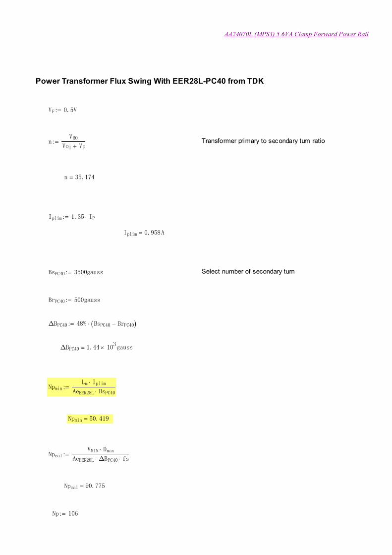
Power Transformer Flux Swing With EER28L-PC40 from TDK
VF 0.5V:=
nVRO
Vo1 VF+:= Transformer primary to secondary turn ratio
n 35.174=
Iplim 1.35 IP:=
Iplim 0.958A=
BsPC40 3500gauss:= Select number of secondary turn
BrPC40 500gauss:=
ΔBPC40 48% BsPC40 BrPC40-( ):=
ΔBPC40 1.44 103
gauss=
NpminLm Iplim
AeEER28L BsPC40:=
Npmin 50.419=
NpcalVMIN Dmax
AeEER28L ΔBPC40 fs:=
Npcal 90.775=
Np 106:=
AA24070L (MPS3) 5.6VA Clamp Forward Power Rail
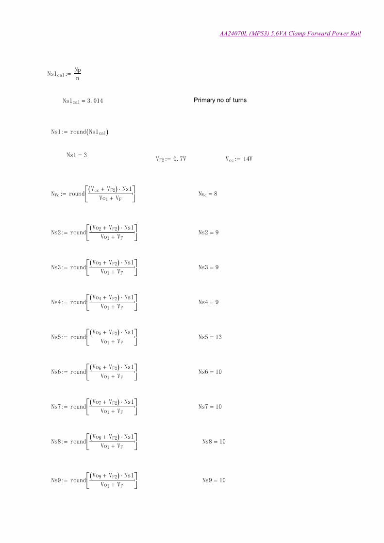
Ns1calNp
n:=
Ns1cal 3.014= Primary no of turns
Ns1 round Ns1cal( ):=
Ns1 3=VF2 0.7V:= Vcc 14V:=
NVc roundVcc VF2+( ) Ns1
Vo1 VF+
:= NVc 8=
Ns2 roundVo2 VF2+( ) Ns1
Vo1 VF+
:= Ns2 9=
Ns3 roundVo3 VF2+( ) Ns1
Vo1 VF+
:= Ns3 9=
Ns4 roundVo4 VF2+( ) Ns1
Vo1 VF+
:= Ns4 9=
Ns5 roundVo5 VF2+( ) Ns1
Vo1 VF+
:= Ns5 13=
Ns6 roundVo6 VF2+( ) Ns1
Vo1 VF+
:= Ns6 10=
Ns7 roundVo7 VF2+( ) Ns1
Vo1 VF+
:= Ns7 10=
Ns8 roundVo8 VF2+( ) Ns1
Vo1 VF+
:= Ns8 10=
Ns9 roundVo9 VF2+( ) Ns1
Vo1 VF+
:= Ns9 10=

AA24070L (MPS3) 5.6VA Clamp Forward Power Rail
Verification of Design Parameters
nactNp
Ns1:=
VROact nact Vo1 VF+( ):=
VROact 194.333V=
Vdson 0.5V:=
D Vg( )nact Vo1 VF+( )
nact Vo1 VF+( ) Vg+ Vdson-:=
DmaxactVROact
VROact VMIN+ Vdson-:=
Dmaxact 0.452=
DminactVROact
VROact VMAX+ Vdson-:=
Dminact 0.343=
Vdsact VMAX VROact+:=
Vdsact 567.686V=
lg μo AeEER28LNp
2
Lm
1
ALEER28L_PC40-
:=
lg 0.726mm=

AA24070L (MPS3) 5.6VA Clamp Forward Power Rail
Lmact Np2 μo μiPC40 AeEER28L
leEER28L μiPC40 lg+:= Nom inductance with ungapped core set
Lmact 1.514mH=
IpactVMIN Dmaxact
Lmact fs:= Ipact 0.705A=
BmLmact Ipact
Np AeEER28L:=
Bm 0.124T=
IpactVMAX Dminact
Lmact fs:= Ipact 0.845A=
BmLmact Ipact
Np AeEER28L:=
Bm 0.148T=
Bpp Vg( )Vg D Vg( )
Np AeEER28L fs:=
Bppmax maxBpp VMAX( )Bpp VMIN( )
:=
Bppmax 0.148T= Check flux density of transformer
Power Transformer Winding Current
ip Vg( )Vg D Vg( )
Lmact fs:= ip VMIN( ) 0.705A=
Vout LsIsp fs
Doff=
IoutIsp Doff
2=
solve Doff, 2 Iout
Isp
AA24070L (MPS3) 5.6VA Clamp Forward Power Rail
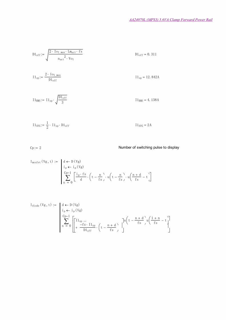
D1off2 Io1_max Lmact fs
nact2
Vo1:= D1off 0.311=
I1sp2 Io1_max
D1off:= I1sp 12.842A=
I1RMS I1spD1off
3:= I1RMS 4.138A=
I1AVG1
2I1sp D1off:= I1AVG 2A=
Cp 2:= Number of switching pulse to display
Imosfet Vg t, ( ) d D Vg( )
ip ip Vg( )
0
Cp 1-
n
ip fs
dt
n
fs-
u tn
fs-
un d+
fst-
=
:=
Idiode Vg t, ( ) d D Vg( )
ip ip Vg( )
0
Cp 1-
n
I1spfs- I1sp
D1offt
n d+
fs-
+
...
u tn d+
fs-
u
1 n+
fst-
=
:=
AA24070L (MPS3) 5.6VA Clamp Forward Power Rail
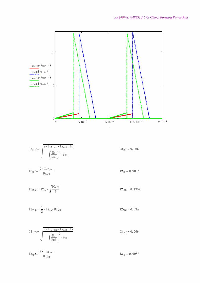
0 5 10 6- 1 10 5- 1.5 10 5- 2 10 5-0
5
10
Imosfet VMIN t, ( )
Idiode VMIN t, ( )
Imosfet VMAX t, ( )
Idiode VMAX t, ( )
t
D2off2 Io2_max Lmact fs
Np
Ns2
2
Vo2
:= D2off 0.066=
I2sp2 Io2_max
D2off:= I2sp 0.908A=
I2RMS I2spD2off
3:= I2RMS 0.135A=
I2AVG1
2I2sp D2off:= I2AVG 0.03A=
D3off2 Io3_max Lmact fs
Np
Ns3
2
Vo3
:= D3off 0.066=
I3sp2 Io3_max
D3off:= I3sp 0.908A=

AA24070L (MPS3) 5.6VA Clamp Forward Power Rail
I3RMS I3spD3off
3:= I3RMS 0.135A=
D4off2 Io4_max Lmact fs
Np
Ns4
2
Vo4
:= D4off 0.209=
I4sp2 Io4_max
D4off:= I4sp 2.872A=
I4RMS I4spD4off
3:= I4RMS 0.758A=
D5off2 Io5_max Lmact fs
Np
Ns5
2
Vo5
:= D5off 0.138=
I5sp2 Io5_max
D5off:= I5sp 1.452A=
I5RMS I5spD5off
3:= I5RMS 0.311A=
D6off2 Io6_max Lmact fs
Np
Ns6
2
Vo6
:= D6off 0.134=
I6sp2 Io6_max
D6off:= I6sp 1.791A=
I6RMS I6spD6off
3:= I6RMS 0.378A=

AA24070L (MPS3) 5.6VA Clamp Forward Power Rail
Evaluate Possible Wire Gauge
Window area should be allocated according to the apparent current of individual winding
IpRMS Vg( )Vg D Vg( )
Lmact fs
D Vg( )
3:=
IpRMS VMIN( ) 0.274A=
Kcutrf 0.2:= Window fill factor
Sm 2.5mm:= Safety creepage distance
Aw BwEER28L 2 Sm-:= Available bobbin breadth
Aw 20.06mm=
Primary winding Np 6 Secondary winding Ns1
AxpriKcutrf AwEER28L
Np:= Axs1
Kcutrf AwEER28L
Ns1 9:=
Axpri 0.182mm2
= Axs1 0.713mm2
=
KJPIpRMS VMIN( )Ax 28( )
:= KJP 3.363A
mm2
= KJs1I1RMS
Ax 28( ) 12:= KJs1 4.238
A
mm2
=
DxpAx 28( ) 4
π:= Dxs1
Ax 28( ) 4
π:=
Dxp 0.322mm= Dxs1 0.322mm=
turn_per_layerpri floorAw
Dxp
:= turn_per_layers1 floorAw
Dxs1 12
:=
turn_per_layerpri 62= turn_per_layers1 5=

AA24070L (MPS3) 5.6VA Clamp Forward Power Rail
Primary winding Np Secondary winding Ns1
layerpri roundNp
turn_per_layerpri
:= layers1 roundNs1
turn_per_layers1
:=
layerpri 2= layers1 1=
StackUppri layerpri Dxp Tape+( ):= StackUpsec 9 layers1 Dxs1 Tape+( ):=
StackUppri 0.764mm= StackUpsec 3.437mm=
TotalStackUpva StackUppri StackUpsec+ 5 Tape+:=
TotalStackUpva 4.501mm=
Resistance per unit length at 100 degC
Rwpri Rx 100 28, ( ):= Rws1 Rx 100 28, ( ):=
Rwpri 2.831 103-
Ω cm1-
= Rws1 2.831 103-
Ω cm1-
=
The dc resistance is then
Rdcpri MLTEER28L Rwpri Np:= Rdcs1 MLTEER28L Rws1Ns1
12:=
Rdcpri 1.319Ω= Rdcs1 3.111mΩ=
The ac resistance is
δskinρ 25( )
π μo fs:=
δskin 0.211mm=
RacpriDxbare 28( )
δskinRdcpri:= Racs1
Dxbare 28( )
δskinRdcs1:=
Racpri 2.011Ω= Racs1 4.742mΩ=

AA24070L (MPS3) 5.6VA Clamp Forward Power Rail
Transformer Copper Loss
Pcutx Vg( ) IpRMS IpRMS Vg( )
IpRMS2
Rdcpri IpRMS2
Racpri+ I1RMS2
Rdcs1 4+
I1RMS2
Racs1 4+
...
:=
Pcutx VMAX( ) 0.809W=
Pcutx VMIN( ) 0.787W=
Transformer Core Loss Estimation
Core loss estimation based on empirical curve fit formula and fit parameters from TDK for PC40 material data within afrequency range of 100 to 200kHz, assumming transformer temperature of 100 degC.
Cm 0.928:=
x 1.61:=
y 2.68:=
Pcoretx Vg( ) Cmfs
Hz
x
Bpp Vg( )
2 T
y
W
m3
VeEER28L:=
Pcoretx VMAX( ) 0.6W= Transformer core loss
Pcoretx VMIN( ) 0.37W=
Total Transformer Losses
Ptx Vg( ) Pcutx Vg( ) Pcoretx Vg( )+:=
Ptx VMAX( ) 1.409W= Power transformer loss at high line, FL
Ptx VMIN( ) 1.157W= Loss at low line, FL

AA24070L (MPS3) 5.6VA Clamp Forward Power Rail
250 300 3501.1
1.2
1.3
1.4
Ptx Vg( )
Vg

AA24070L (MPS3) 5.6VA Clamp Forward Power Rail
Secondary Rectifier Stress
Vs1diode Vo1 VMAXNs1
Np+:= Vs1diode 15.567V=
Vs2diode Vo2 VMAXNs2
Np+:= Vs2diode 46.7V=
Vs3diode Vo3 VMAXNs3
Np+:= Vs3diode 46.7V=
Vs4diode Vo4 VMAXNs4
Np+:= Vs4diode 46.7V=
Vs5diode Vo5 VMAXNs5
Np+:= Vs5diode 69.788V=
Vs6diode Vo6 VMAXNs6
Np+:= Vs6diode 53.222V=
Vs7diode Vo7 VMAXNs7
Np+:= Vs7diode 53.222V=
Vcdiode Vcc VMAXNVc
Np+:= Vcdiode 42.178V=
Pdrectifier VF Io1_max VF2 Io2_max+ VF2 Io3_max+ VF2 Io4_max+ VF2 Io5_max+ 4 VF2 Io6_max+:=
Pdrectifier 1.658W=
AA24070L (MPS3) 5.6VA Clamp Forward Power Rail
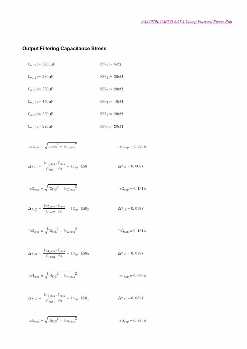
Output Filtering Capacitance Stress
Cout1 2200μF:= ESR1 5mΩ:=
Cout2 220μF:= ESR2 20mΩ:=
Cout3 220μF:= ESR3 20mΩ:=
Cout4 440μF:= ESR4 10mΩ:=
Cout5 220μF:= ESR5 20mΩ:=
Cout6 220μF:= ESR6 20mΩ:=
Is1cap I1RMS2
Io1_max2
-:= Is1cap 3.623A=
ΔVs1Io1_max Dmax
Cout1 fsI1sp ESR1+:= ΔVs1 0.068V=
Is2cap I2RMS2
Io2_max2
-:= Is2cap 0.131A=
ΔVs2Io2_max Dmax
Cout2 fsI2sp ESR2+:= ΔVs2 0.019V=
Is3cap I3RMS2
Io3_max2
-:= Is3cap 0.131A=
ΔVs3Io3_max Dmax
Cout3 fsI3sp ESR3+:= ΔVs3 0.019V=
Is4cap I4RMS2
Io4_max2
-:= Is4cap 0.696A=
ΔVs4Io4_max Dmax
Cout4 fsI4sp ESR4+:= ΔVs4 0.032V=
Is5cap I5RMS2
Io5_max2
-:= Is5cap 0.295A=

AA24070L (MPS3) 5.6VA Clamp Forward Power Rail
ΔVs5Io5_max Dmax
Cout5 fsI5sp ESR5+:= ΔVs5 0.031V=
Is6cap I6RMS2
Io6_max2
-:= Is6cap 0.359A=
ΔVs6Io6_max Dmax
Cout6 fsI6sp ESR6+:= ΔVs6 0.038V=
Capacitance requirement - Transient response dependence
τ 15 Ts:= Assume delay time before converter response to a changein load current
ΔVocapΔIo
Coτ= Capacitive voltage change due to load step
ΔVoesr ΔIo Resr= Voltage change across esr due to a load step
ΔVo ΔVocap ΔVoesr+= Output voltage change due to a load step ignoring effect ofESL
ΔVoΔIo
Coτ ΔIo Resr+=
Coτ
ΔVo
ΔIoResr-
> Capacitance required for a voltage deviation of DVo withsay Resr
no_of_cap 1:= Select number of capacitor required
ResrESR1
no_of_cap:=
Resr 5mΩ= Effective ESR with capacitor chosen
Capacitor ripple current and effective current handling capacity
ΔIcap I1RMS2
Io1_max2
-:= AC rms current seen by cap
ΔIcap 3.623A=

AA24070L (MPS3) 5.6VA Clamp Forward Power Rail
Output ripple voltage with selected capacitors
ΔVr I1sp ESR1:= Output ripple voltage due to esr
ΔVr 64.21mV= Maximum output voltage ripple at room temperature
At low temperature, esr of capacitor changes significantly
Resrlotemp Resr 2:=
Resrlotemp 0.01Ω=
ΔVrlotemp ΔIcap Resrlotemp:=
ΔVrlotemp 0.036V= Maximum output ripple at low temperature
κripple 1ΔVrlotemp
Vr-:=
κripple 63.775%= Ripple voltage design margin at low temperature
Step load ripple voltage
Comin no_of_cap Cout1 1 10%-( ):=
ΔVo ΔIo5V Resrlotempτ
Comin+
:= Voltage change due to step load
ΔVo 0.137V=
κstep 1ΔVo
ΔVostep-:=
κstep 8.525%= Step response ripple deviation design margin at lowtemperature
Estimate Power Loss In Capacitor ESR
Pesr Vg( )ΔIcap
2
1
3
2
Resr:=
Pesr VMAX( ) 5.468mW=
AA24070L (MPS3) 5.6VA Clamp Forward Power Rail
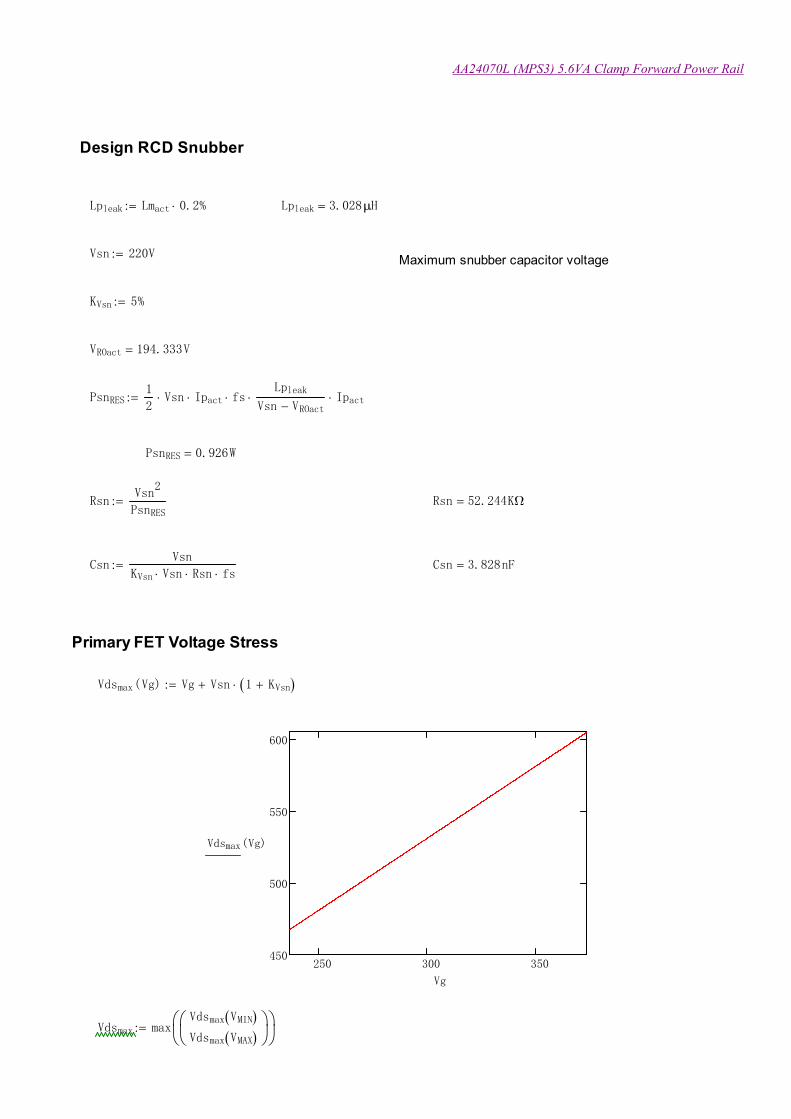
Design RCD Snubber
Lpleak Lmact 0.2 %:= Lpleak 3.028μH=
Vsn 220V:=Maximum snubber capacitor voltage
KVsn 5%:=
VROact 194.333V=
PsnRES1
2Vsn Ipact fs
Lpleak
Vsn VROact- Ipact:=
PsnRES 0.926W=
RsnVsn
2
PsnRES:= Rsn 52.244KΩ=
CsnVsn
KVsn Vsn Rsn fs:= Csn 3.828nF=
Primary FET Voltage Stress
Vdsmax Vg( ) Vg Vsn 1 KVsn+( )+:=
250 300 350450
500
550
600
Vdsmax Vg( )
Vg
Vdsmax maxVdsmax VMIN( )Vdsmax VMAX( )
:=

AA24070L (MPS3) 5.6VA Clamp Forward Power Rail
Vdsmax 604.352V= Peak switch voltage stress at high line

AA24070L (MPS3) 5.6VA Clamp Forward Power Rail
Primary Switch Current
Main FET conducts the transformer primary current
IQ Vg t, ( ) Imosfet Vg t, ( ):= Main switch current
IQRMS Vg( )Vg D Vg( )
Lmact fs
D Vg( )
3:= Main switch rms current
IQpk Vg( )Vg D Vg( )
Lmact fs:= Main switch peak current
Primary FET Loss Estimation - IRFBC30A
Gate drive loss
Vgate 10V:= Gate drive voltage
Pgate Vgate Qgirfbc30a fs:=
Pgate 0.023W= Gate drive loss
Saturation loss
PQon Vg( ) IQRMS Vg( )2
Ronirfbc30a:=
PQon VMAX( ) 0.305W= Saturation loss at high line, FL
PQon VMIN( ) 0.28W=
Output capacitance loss
PQcap Vg( )1
2Coss_effirfbc30a Vg
2 fs:=
PQcap Vgmax( ) 0.244W= Output capacitance loss at high line
AA24070L (MPS3) 5.6VA Clamp Forward Power Rail
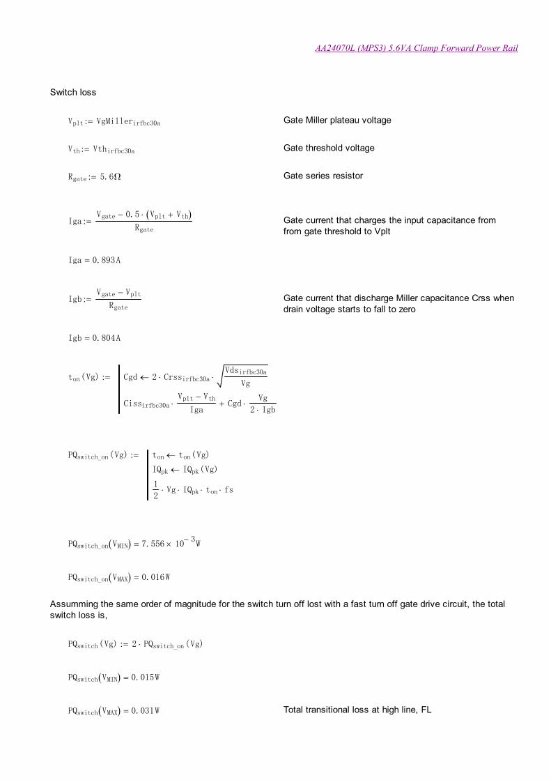
Switch loss
Vplt VgMillerirfbc30a:= Gate Miller plateau voltage
Vth Vthirfbc30a:= Gate threshold voltage
Rgate 5.6Ω:= Gate series resistor
IgaVgate 0.5 Vplt Vth+( )-
Rgate:= Gate current that charges the input capacitance from
from gate threshold to Vplt
Iga 0.893A=
IgbVgate Vplt-
Rgate:= Gate current that discharge Miller capacitance Crss when
drain voltage starts to fall to zero
Igb 0.804A=
ton Vg( ) Cgd 2 Crssirfbc30aVdsirfbc30a
Vg
Cissirfbc30aVplt Vth-
Iga Cgd
Vg
2 Igb+
:=
PQswitch_on Vg( ) ton ton Vg( )
IQpk IQpk Vg( )
1
2Vg IQpk ton fs
:=
PQswitch_on VMIN( ) 7.556 103-
W=
PQswitch_on VMAX( ) 0.016W=
Assumming the same order of magnitude for the switch turn off lost with a fast turn off gate drive circuit, the totalswitch loss is,
PQswitch Vg( ) 2 PQswitch_on Vg( ):=
PQswitch VMIN( ) 0.015W=
PQswitch VMAX( ) 0.031W= Total transitional loss at high line, FL
AA24070L (MPS3) 5.6VA Clamp Forward Power Rail
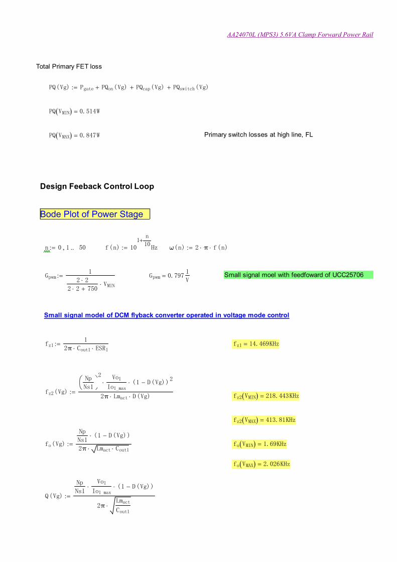
Total Primary FET loss
PQ Vg( ) Pgate PQon Vg( )+ PQcap Vg( )+ PQswitch Vg( )+:=
PQ VMIN( ) 0.514W=
PQ VMAX( ) 0.847W= Primary switch losses at high line, FL
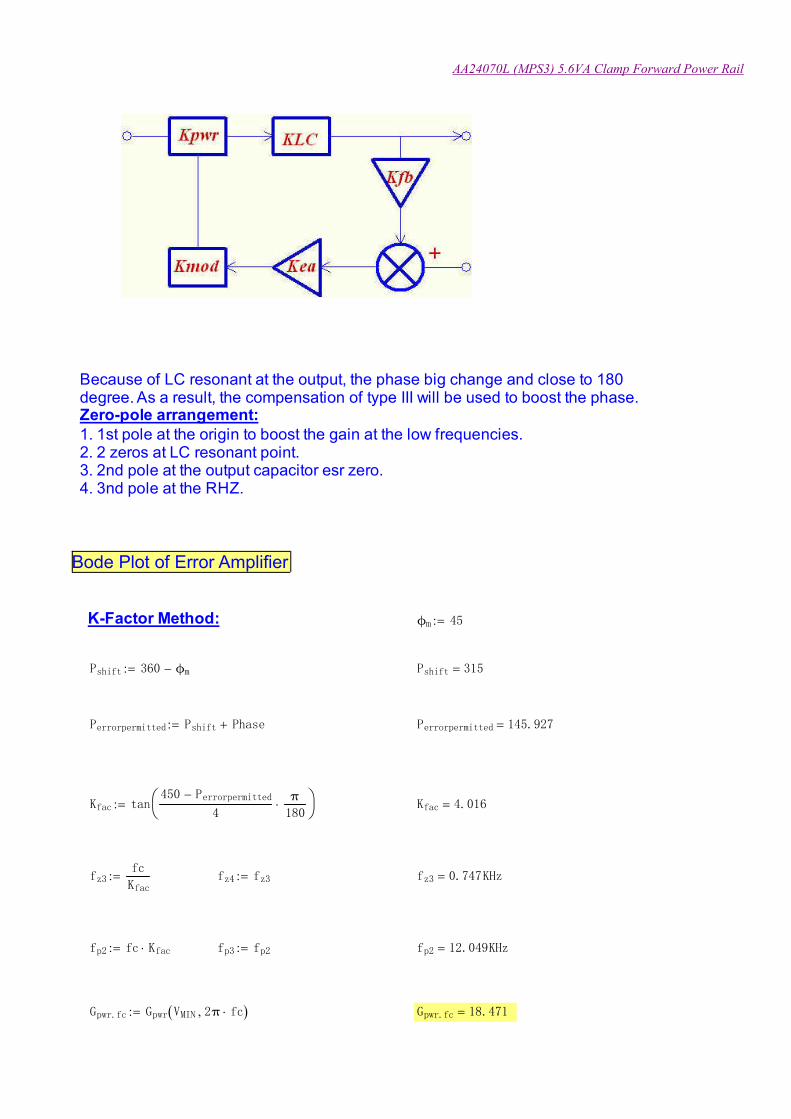
Design Feeback Control Loop
Bode Plot of Power Stage
n 0 1, 50..:= f n( ) 101
n
10+
Hz:= ω n( ) 2 π f n( ):=
Gpwm1
2 2
2 2 750+VMIN
:= Gpwm 0.7971
V= Small signal moel with feedfoward of UCC25706
Small signal model of DCM flyback converter operated in voltage mode control
fz11
2π Cout1 ESR1:= fz1 14.469KHz=
fz2 Vg( )
Np
Ns1
2 Vo1
Io1_max 1 D Vg( )-( )
2
2π Lmact D Vg( ):=
fz2 VMIN( ) 218.443KHz=
fz2 VMAX( ) 413.81KHz=
fo Vg( )
Np
Ns11 D Vg( )-( )
2π Lmact Cout1:= fo VMIN( ) 1.69KHz=
fo VMAX( ) 2.026KHz=
Q Vg( )
Np
Ns1
Vo1
Io1_max 1 D Vg( )-( )
2πLmact
Cout1
:=

AA24070L (MPS3) 5.6VA Clamp Forward Power Rail
Gdo Vg( )Vg
Np
Ns11 D Vg( )-( )
2
:=
Tpwr Vg ω, ( )
Gpwm Gdo Vg( ) 1i ω
2π fz1+
1i ω
2π fz2 Vg( )-
1i ω
2π fo Vg( ) Q Vg( )+
ω2
2π fo Vg( )( )2-
:=
Gpwr Vg ω, ( ) 20 log Tpwr Vg ω, ( )( ):=Ppwr Vg ω, ( )
180
π
arg Tpwr Vg ω, ( )( ):=
Gpwrmin ω( ) Gpwr VMIN ω, ( ):= Ppwrmin ω( ) Ppwr VMIN ω, ( ):=
Gpwrmax ω( ) Gpwr VMAX ω, ( ):= Ppwrmax ω( ) Ppwr VMAX ω, ( ):=
10 100 1 103 1 104 1 105 1 10640-
28.75-
17.5-
6.25-
5
16.25
27.5
38.75
50Power Gain
Frequency
Gain
- dB
AA24070L (MPS3) 5.6VA Clamp Forward Power Rail
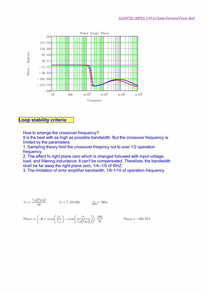
10 100 1 103 1 104 1 105 1 106200-
152.778-
105.556-
58.333-
11.111-
36.111
83.333
130.556
177.778
225Power Stage Phase
Frequency
Phase
-
Degree
s
Loop stability criteria
How to arrange the crossover frequency?It is the best with as high as possible bandwidth. But the crossover frequency islimited by the parameters:1. Sampling theory limit the crossover freqency not to over 1/2 operationfrequency.2. The effect fo right plane zero which is changed followed with input voltage,load, and filtering inductance. It can't be compensated. Therefore, the bandwidthshall be far away the right plane zero, 1/4--1/5 of RHZ.3. The limitation of error amplifier bandwidth. 1/6-1/10 of operation frequency.
fcfz2 VMIN( )
30:= fc 7.281KHz= fc 3KHz:=
Phase π- atanfc
fz1
+ atanfc
fz2 VMIN( )
-
180
π:= Phase 169.073-=
AA24070L (MPS3) 5.6VA Clamp Forward Power Rail
Because of LC resonant at the output, the phase big change and close to 180degree. As a result, the compensation of type III will be used to boost the phase. Zero-pole arrangement:1. 1st pole at the origin to boost the gain at the low frequencies.2. 2 zeros at LC resonant point.3. 2nd pole at the output capacitor esr zero.4. 3nd pole at the RHZ.
Bode Plot of Error Amplifier
K-Factor Method: ϕm 45:=
Pshift 360 ϕm-:= Pshift 315=
Perrorpermitted Pshift Phase+:= Perrorpermitted 145.927=
Kfac tan450 Perrorpermitted-
4
π180
:= Kfac 4.016=
fz3fc
Kfac:= fz4 fz3:= fz3 0.747KHz=
fp2 fc Kfac:= fp3 fp2:= fp2 12.049KHz=
Gpwr.fc Gpwr VMIN 2π fc, ( ):= Gpwr.fc 18.471=
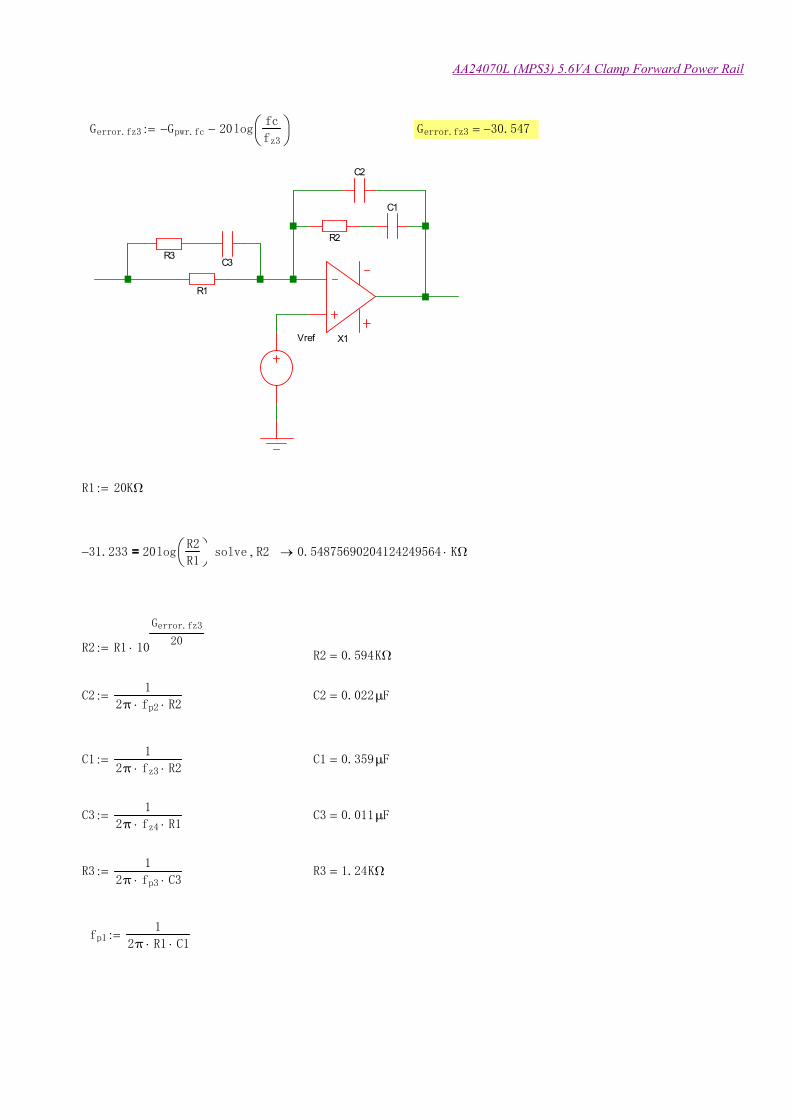
AA24070L (MPS3) 5.6VA Clamp Forward Power Rail
Gerror.fz3 Gpwr.fc- 20logfc
fz3
-:= Gerror.fz3 30.547-=
X1
C2
R3
C1
R1
R2
C3
Vref
R1 20KΩ:=
31.233- 20logR2
R1
= solve R2, 0.54875690204124249564 KΩ
R2 R1 10
Gerror.fz3
20:=
R2 0.594KΩ=
C21
2π fp2 R2:= C2 0.022μF=
C11
2π fz3 R2:= C1 0.359μF=
C31
2π fz4 R1:= C3 0.011μF=
R31
2π fp3 C3:= R3 1.24KΩ=
fp11
2π R1 C1:=
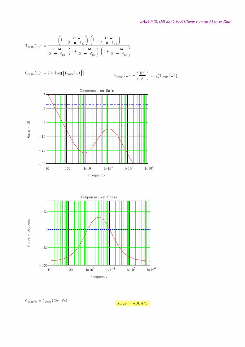
AA24070L (MPS3) 5.6VA Clamp Forward Power Rail
Tcomp ω( )
1i ω
2 π fz3+
1i ω
2 π fz4+
i ω
2 π fp11
i ω
2 π fp2+
1i ω
2 π fp3+
:=
Gcomp ω( ) 20 log Tcomp ω( )( ):=Pcomp ω( )
180
π
arg Tcomp ω( )( ):=
10 100 1 103 1 104 1 105 1 10630-
23-
16-
9-
2-
5Compensation Gain
Frequency
Gain -
dB
10 100 1 103 1 104 1 105 1 106100-
50-
0
50
Compensation Phase
Frequency
Pha
se -
Deg
rees
Gcompfc Gcomp 2π fc( ):=Gcompfc 18.471-=

AA24070L (MPS3) 5.6VA Clamp Forward Power Rail
Bode Plot of Closed-Loop
Tloop Vin ω, ( ) Tcomp ω( ) Tpwr Vin ω, ( ):=
Gloop Vin ω, ( ) 20 log Tloop Vin ω, ( )( ):= Ploop Vin ω, ( )180
π
arg Tloop Vin ω, ( )( ):=
Gmaxmax ω( ) Gloop VMAX ω, ( ):= Gminmax ω( ) Gloop VMIN ω, ( ):=
Pminmax ω( ) Ploop VMIN ω, ( ):= Pmaxmax ω( ) Ploop VMAX ω, ( ):=
10 100 1 103 1 104 1 105 1 10650-
39.375-
28.75-
18.125-
7.5-
3.125
13.75
24.375
35
Min VinMax Vin0 dB
Loop Gain
Frequency
Gain -
dB
AA24070L (MPS3) 5.6VA Clamp Forward Power Rail
10 100 1 103 1 104 1 105 1 106180-
135-
90-
45-
0
45
90
135
180Loop Phase
Frequency
Phase
-
Degree
s
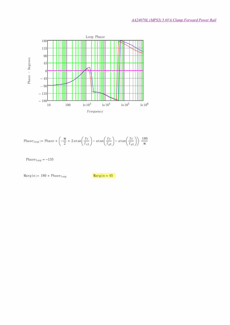
Phaseloop Phaseπ2
- 2atanfc
fz3
+ atanfc
fp2
- atanfc
fp3
-
180
π+:=
Phaseloop 135-=
Margin 180 Phaseloop+:= Margin 45=

AA24070L (MPS3) 5.6VA Clamp Forward Power Rail

AA24070L (MPS3) 5.6VA Clamp Forward Power Rail
Winding area base on BEE35-1112CPLFR standard bobbin

AA24070L (MPS3) 5.6VA Clamp Forward Power Rail
Winding area base on BEE33-1112CPLFR standard bobbin
Winding area base on BE30-1110CPFR standard bobbin

AA24070L (MPS3) 5.6VA Clamp Forward Power Rail
Secondary winding Ns4
Axs4Kcutrf AwEER28L
Ns4 9:=
Axs4 0.238mm2
=
KJs4I4RMS
Ax 28( ) 3:= KJs4 3.105
A
mm2
=
Dxs4Ax 28( ) 4
π:=
Dxs4 0.322mm=
turn_per_layers4 floorAw
Dxs4 3
:=
turn_per_layers4 20=

AA24070L (MPS3) 5.6VA Clamp Forward Power Rail
Secondary winding Ns4
layers4 roundNs4
turn_per_layers40.05+
:=
layers4 1=
Rws4 Rx 100 28, ( ):=
Rws4 2.831 103-
Ω cm1-
=
Rdcs4 MLTEER28L Rws4Ns4
3:=
Rdcs4 37.331mΩ=
Racs4Dxbare 28( )
δskinRdcs4:=
Racs4 56.905mΩ=

AA24070L (MPS3) 5.6VA Clamp Forward Power Rail
Core loss estimation based on empirical curve fit formula and fit parameters from TDK for PC40 material data within a

AA24070L (MPS3) 5.6VA Clamp Forward Power Rail
Assume delay time before converter response to a change
Output voltage change due to a load step ignoring effect of

AA24070L (MPS3) 5.6VA Clamp Forward Power Rail

AA24070L (MPS3) 5.6VA Clamp Forward Power Rail

AA24070L (MPS3) 5.6VA Clamp Forward Power Rail