2.5v to 6.0v micropower cmos op amps...
TRANSCRIPT

MCP606/7/8/92.5V to 6.0V Micropower CMOS Op Amp
Features• Low Input Offset Voltage: 250 µV (maximum)• Rail-to-Rail Output• Low Input Bias Current: 80 pA (maximum at
+85°C)• Low Quiescent Current: 25 µA (maximum)• Power Supply Voltage: 2.5V to 6.0V• Unity-Gain Stable• Chip Select (CS) Capability: MCP608• Industrial Temperature Range: -40°C to +85°C• No Phase Reversal• Available in Single, Dual and Quad Packages
Typical Applications• Battery Power Instruments• High-Impedance Applications• Strain Gauges• Medical Instruments• Test Equipment
Design Aids• SPICE Macro Models• FilterLab® Software• Mindi™ Circuit Designer & Simulator• Analog Demonstration and Evaluation Boards• Application Notes
Typical Application
DescriptionThe MCP606/7/8/9 family of operational amplifiers (opamps) from Microchip Technology Inc. are unity-gainstable with low offset voltage (250 µV, maximum).Performance characteristics include rail-to-rail outputswing capability and low input bias current (80 pA at+85°C, maximum). These features make this family ofop amps well suited for single-supply, precision,high-impedance, battery-powered applications.
The single is available in standard 8-lead PDIP, SOICand TSSOP packages, as well as in a SOT-23-5package. The single MCP608 with Chip Select (CS) isoffered in the standard 8-lead PDIP, SOIC and TSSOPpackages. The dual MCP607 is offered in the standard8-lead PDIP, SOIC and TSSOP packages. Finally, thequad MCP609 is offered in the standard 14-lead PDIP,SOIC and TSSOP packages. All devices are fullyspecified from -40°C to +85°C, with power suppliesfrom 2.5V to 6.0V.
Package Types
Low-Side Battery Current Sensor
RF
To Load
2.5V
RG5 kΩ 50 kΩ
To Load
VOUT
RSEN10Ω (VLM)
(VLP)
IL
to6.0V
VOUT VLM I+ LRSEN RF RG⁄( )=
MCP606
VIN+VIN–
VSS
VDDVOUT
1234
8765 NC
NCNC
PDIP, SOIC,TSSOP
PDIP, SOIC,TSSOP PDIP, SOIC,TSSOP
PDIP, SOIC,TSSOP
SOT-23-5
VIN+VSS
VIN–
123
5
4
VDDVOUT
VINA+VINA–
VSS
VOUTBVINB–
1234
8765 VINB+
VDDVOUTA
VIN+VIN–
VSS
VDDVOUT
1234
8765 NC
CSNC
VINA+VINA–
VDD
VIND–VIND+
1234
14131211 VSS
VOUTDVOUTA
VINB–VINB+
VOUTB
VINC+VINC–
567
1098 VOUTC
MCP606 MCP606
MCP607 MCP608
MCP609
© 2009 Microchip Technology Inc. DS11177F-page 1

MCP606/7/8/9
NOTES:DS11177F-page 2 © 2009 Microchip Technology Inc.

MCP606/7/8/9
1.0 ELECTRICAL CHARACTERISTICS
Absolute Maximum Ratings †VDD – VSS ........................................................................7.0VCurrent at Input Pins ....................................................±2 mAAnalog Inputs (VIN+, VIN–) †† ........ VSS – 1.0V to VDD + 1.0VAll Other Inputs and Outputs ......... VSS – 0.3V to VDD + 0.3VDifference Input Voltage ...................................... |VDD – VSS|Output Short Circuit Current ................................ContinuousCurrent at Output and Supply Pins ............................±30 mAStorage Temperature .................................–65° C to +150° CMaximum Junction Temperature (TJ)........................ .+150° CESD Protection On All Pins (HBM; MM) .............. ≥ 3 kV; 200V
† Notice: Stresses above those listed under “AbsoluteMaximum Ratings” may cause permanent damage to thedevice. This is a stress rating only and functional operation ofthe device at those or any other conditions above thoseindicated in the operational listings of this specification is notimplied. Exposure to maximum rating conditions for extendedperiods may affect device reliability.†† See Section 4.1.2 “Input Voltage and Current Limits”.
DC CHARACTERISTICSElectrical Characteristics: Unless otherwise indicated, VDD = +2.5V to +5.5V, VSS = GND, TA = +25°C, VCM = VDD/2,VOUT ≈ VDD/2, VL = VDD/2, RL = 100 kΩ to VL, and CS is tied low (refer to Figure 1-2 and Figure 1-3).
Parameters Sym Min Typ Max Units Conditions
Input OffsetInput Offset Voltage VOS -250 — +250 µVInput Offset Drift with Temperature ΔVOS/ΔTA — ±1.8 — µV/°C TA = -40°C to +85°CPower Supply Rejection Ratio PSRR 80 93 — dBInput Bias Current and ImpedanceInput Bias Current IB — 1 — pA
At Temperature IB — — 80 pA TA = +85°CInput Offset Bias Current IOS — 1 — pACommon Mode Input Impedance ZCM — 1013||6 — Ω||pFDifferential Input Impedance ZDIFF — 1013||6 — Ω||pFCommon ModeCommon Mode Input Range VCMR VSS – 0.3 VDD – 1.1 V CMRR ≥ 75 dBCommon Mode Rejection Ratio CMRR 75 91 — dB VDD = 5V, VCM = -0.3V to 3.9VOpen-Loop GainDC Open-Loop Gain(Large-signal)
AOL 105 121 — dB RL = 25 kΩ to VL, VOUT = 50 mV to VDD – 50 mV
DC Open-Loop Gain(Large-signal)
AOL 100 118 — dB RL = 5 kΩ to VL, VOUT = 0.1V to VDD – 0.1V
OutputMaximum Output Voltage Swing VOL, VOH VSS + 15 — VDD – 20 mV RL = 25 kΩ to VL,
0.5V input overdriveVOL, VOH VSS + 45 — VDD – 60 mV RL = 5 kΩ to VL,
0.5V input overdriveLinear Output Voltage Range VOUT VSS + 50 — VDD – 50 mV RL = 25 kΩ to VL,
AOL ≥ 105 dBVOUT VSS + 100 — VDD – 100 mV RL = 5 kΩ to VL,
AOL ≥ 100 dBOutput Short Circuit Current ISC — 7 — mA VDD = 2.5V
ISC — 17 — mA VDD = 5.5VPower SupplySupply Voltage VDD 2.5 — 6.0 VQuiescent Current per Amplifier IQ — 18.7 25 µA IO = 0Note 1: All parts with date codes November 2007 and later have been screened to ensure operation at VDD = 6.0V. However,
the other minimum and maximum specifications are measured at 2.5V and 5.5V.
© 2009 Microchip Technology Inc. DS11177F-page 3
MCP606/7/8/9
AC CHARACTERISTICS
MCP608 CHIP SELECT CHARACTERISTICS
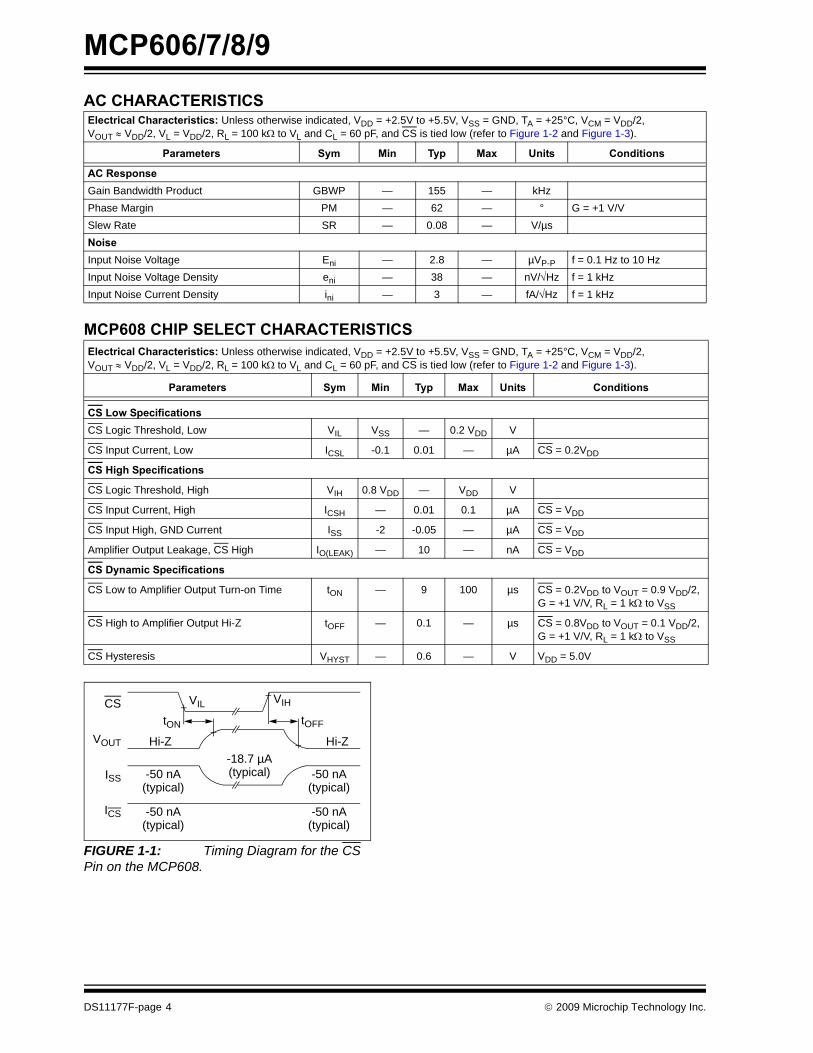
FIGURE 1-1: Timing Diagram for the CS Pin on the MCP608.
Electrical Characteristics: Unless otherwise indicated, VDD = +2.5V to +5.5V, VSS = GND, TA = +25°C, VCM = VDD/2,VOUT ≈ VDD/2, VL = VDD/2, RL = 100 kΩ to VL and CL = 60 pF, and CS is tied low (refer to Figure 1-2 and Figure 1-3).
Parameters Sym Min Typ Max Units Conditions
AC ResponseGain Bandwidth Product GBWP — 155 — kHzPhase Margin PM — 62 — ° G = +1 V/VSlew Rate SR — 0.08 — V/µsNoiseInput Noise Voltage Eni — 2.8 — µVP-P f = 0.1 Hz to 10 HzInput Noise Voltage Density eni — 38 — nV/√Hz f = 1 kHzInput Noise Current Density ini — 3 — fA/√Hz f = 1 kHz
Electrical Characteristics: Unless otherwise indicated, VDD = +2.5V to +5.5V, VSS = GND, TA = +25°C, VCM = VDD/2,VOUT ≈ VDD/2, VL = VDD/2, RL = 100 kΩ to VL and CL = 60 pF, and CS is tied low (refer to Figure 1-2 and Figure 1-3).
Parameters Sym Min Typ Max Units Conditions
CS Low SpecificationsCS Logic Threshold, Low VIL VSS — 0.2 VDD V
CS Input Current, Low ICSL -0.1 0.01 — µA CS = 0.2VDD
CS High Specifications
CS Logic Threshold, High VIH 0.8 VDD — VDD V
CS Input Current, High ICSH — 0.01 0.1 µA CS = VDD
CS Input High, GND Current ISS -2 -0.05 — µA CS = VDD
Amplifier Output Leakage, CS High IO(LEAK) — 10 — nA CS = VDD
CS Dynamic Specifications
CS Low to Amplifier Output Turn-on Time tON — 9 100 µs CS = 0.2VDD to VOUT = 0.9 VDD/2,G = +1 V/V, RL = 1 kΩ to VSS
CS High to Amplifier Output Hi-Z tOFF — 0.1 — µs CS = 0.8VDD to VOUT = 0.1 VDD/2,G = +1 V/V, RL = 1 kΩ to VSS
CS Hysteresis VHYST — 0.6 — V VDD = 5.0V
CS
VOUT
ISS
ICS
VIL VIH
tON tOFF
-50 nA -50 nA-18.7 µA
-50 nA -50 nA
Hi-Z Hi-Z
(typical)(typical)
(typical)
(typical) (typical)
DS11177F-page 4 © 2009 Microchip Technology Inc.

MCP606/7/8/9
TEMPERATURE CHARACTERISTICS
1.1 Test CircuitsThe test circuits used for the DC and AC tests areshown in Figure 1-2 and Figure 1-3. The bypasscapacitors are laid out according to the rules discussedin Section 4.5 “Supply Bypass”.
FIGURE 1-2: AC and DC Test Circuit for Most Non-Inverting Gain Conditions.
FIGURE 1-3: AC and DC Test Circuit for Most Inverting Gain Conditions.
Electrical Characteristics: Unless otherwise indicated, VDD = +2.5V to +5.5V and VSS = GND.
Parameters Sym Min Typ Max Units Conditions
Temperature RangesSpecified Temperature Range TA -40 — +85 °COperating Temperature Range TA -40 — +125 °C Note 1Storage Temperature Range TA -65 — +150 °CThermal Package ResistancesThermal Resistance, 5L-SOT23 θJA — 220.7 — °C/WThermal Resistance, 8L-PDIP θJA — 89.3 — °C/WThermal Resistance, 8L-SOIC θJA — 149.5 — °C/WThermal Resistance, 8L-TSSOP θJA — 139 — °C/WThermal Resistance, 14L-PDIP θJA — 70 — °C/WThermal Resistance, 14L-SOIC θJA — 95.3 — °C/WThermal Resistance, 14L-TSSOP θJA — 100 — °C/WNote 1: The MCP606/7/8/9 operate over this extended temperature range, but with reduced performance. In any case, the
Junction Temperature (TJ) must not exceed the Absolute Maximum specification of +150°C.
VDD
RG RF
RNVOUT
VIN
VDD/2
1 µF
CL RL
VL
0.1 µF
MCP60X
VDD
RG RF
RNVOUT
VDD/2
VIN
1 µF
CL RL
VL
0.1 µF
MCP60X
© 2009 Microchip Technology Inc. DS11177F-page 5

MCP606/7/8/9
NOTES:DS11177F-page 6 © 2009 Microchip Technology Inc.

MCP606/7/8/9
2.0 TYPICAL PERFORMANCE CURVES
Note: Unless otherwise indicated, VDD = +2.5V to +5.5V, VSS = GND, TA = +25°C, VCM = VDD/2, VOUT ≈ VDD/2,VL = VDD/2, RL = 100 kΩ to VL, CL = 60 pF, and CS is tied low.
FIGURE 2-1: Input Offset Voltage at VDD = 5.5V.
FIGURE 2-2: Input Offset Voltage at VDD = 2.5V.
FIGURE 2-3: Quiescent Current vs. Power Supply Voltage.
FIGURE 2-4: Input Offset Voltage Drift Magnitude at VDD = 5.5V.
FIGURE 2-5: Input Offset Voltage Drift Magnitude at VDD = 2.5V.
FIGURE 2-6: Quiescent Current vs. Ambient Temperature.
Note: The graphs and tables provided following this note are a statistical summary based on a limited number ofsamples and are provided for informational purposes only. The performance characteristics listed hereinare not tested or guaranteed. In some graphs or tables, the data presented may be outside the specifiedoperating range (e.g., outside specified power supply range) and therefore outside the warranted range.
0%2%4%6%8%
10%12%14%16%
-250
-200
-150
-100 -50 0 50 100
150
200
250
Input Offset Voltage (µV)
Perc
enta
ge o
f Occ
uran
ces
( )
1200 SamplesVDD = 5.5V
0%2%4%6%8%
10%12%14%16%
-250
-200
-150
-100 -5
0 0 50 100
150
200
250
Input Offset Voltage (µV)
Perc
enta
ge o
f Occ
uran
ces
( )
1200 SamplesVDD = 2.5V
02468
10121416182022
0.0 0.5 1.0 1.5 2.0 2.5 3.0 3.5 4.0 4.5 5.0 5.5Power Supply Voltage (V)
Qui
esce
nt C
urre
nt
per A
mpl
ifier
(µA
)
TA = +85°CTA = +25°CTA = -40°C
0%
2%
4%
6%
8%
10%
12%
14%
16%
-8 -6 -4 -2 0 2 4 6 8Input Offset Voltage Drift (µV/°C)
Perc
enta
ge o
f Occ
uran
ces 206 Samples
VDD = 5.5V
0%2%4%6%8%
10%12%14%16%18%
-8 -6 -4 -2 0 2 4 6 8Input Offset Voltage Drift (µV/°C)
Perc
enta
ge o
f Occ
uran
ces 206 Samples
VDD = 2.5V
12
14
16
18
20
22
24
-50 -25 0 25 50 75 100Ambient Temperature (°C)
Qui
esce
nt C
urre
ntpe
r Am
plifi
er (µ
A)
VDD = 5.5V
VDD = 2.5V
© 2009 Microchip Technology Inc. DS11177F-page 7

MCP606/7/8/9
Note: Unless otherwise indicated, VDD = +2.5V to +5.5V, VSS = GND, TA = +25°C, VCM = VDD/2, VOUT ≈ VDD/2,VL = VDD/2, RL = 100 kΩ to VL, CL = 60 pF, and CS is tied low.FIGURE 2-7: Input Offset Voltage vs. Ambient Temperature.
FIGURE 2-8: Open-Loop Gain and Phase vs. Frequency.
FIGURE 2-9: Channel-to-Channel Separation (MCP607 and MCP609 only).
FIGURE 2-10: Input Offset Voltage vs. Common Mode Input Voltage.
FIGURE 2-11: Gain Bandwidth Product, Phase Margin vs. Ambient Temperature.
FIGURE 2-12: Input Noise Voltage Density vs. Frequency.
0
100
200
300
400
500
-50 -25 0 25 50 75 100Ambient Temperature (°C)
Inpu
t Offs
et V
olta
ge (µ
V) VDD =2.5VVDD = 5.5V
Representative Part
-20
0
20
40
60
80
100
120
Frequency (Hz)
Ope
n-Lo
op G
ain
(dB
)
-225
-180
-135
-90
-45
0
45
90
Ope
n-Lo
op P
hase
(°)
Gain
Phase
RL = 25 kΩ
0.01 10.1 10 1k100 10k 1M100k
80
90
100
110
120
130
140
1.E+02 1.E+03 1.E+04 1.E+05Frequency (Hz)
Cha
nnel
to C
hann
el
Sepa
ratio
n (d
B)
Referred to Input
100 100k10k1k
-20
0
20
40
60
80
100
120
-0.5 0.0
0.5
1.0
1.5
2.0
2.5
3.0
3.5
4.0
4.5
5.0
Common Mode Input Voltage (V)
Inpu
t Offs
et V
olta
ge (µ
V)
TA = +85°CTA = +25°CTA = -40°C
VDD = 5.5V
020406080
100120140160
-50 -25 0 25 50 75 100Ambient Temperature (°C)
Gai
n B
andw
idth
Pro
duct
(kH
z)
01020304050607080
Phas
e M
argi
n (°
)
Phase Margin
GBWP
VDD = 5.0V
10
100
1000
1.E-01 1.E+00 1.E+01 1.E+02 1.E+03 1.E+04 1.E+05Frequency (Hz)
Inpu
t Noi
se V
olta
ge D
ensi
ty(n
V/√H
z)
0.1 1 10 100 1k 10k 100k
DS11177F-page 8 © 2009 Microchip Technology Inc.

MCP606/7/8/9
Note: Unless otherwise indicated, VDD = +2.5V to +5.5V, VSS = GND, TA = +25°C, VCM = VDD/2, VOUT ≈ VDD/2,VL = VDD/2, RL = 100 kΩ to VL, CL = 60 pF, and CS is tied low.FIGURE 2-13: Input Bias Current, Input Offset Current vs. Ambient Temperature.
FIGURE 2-14: DC Open-Loop Gain vs. Load Resistance.
FIGURE 2-15: CMRR, PSRR vs. Frequency.
FIGURE 2-16: Input Bias Current, Input Offset Current vs. Common Mode Input Voltage.
FIGURE 2-17: DC Open-Loop Gain vs. Power Supply Voltage.
FIGURE 2-18: CMRR, PSRR vs. Ambient Temperature.
0.1
1
10
100
25 30 35 40 45 50 55 60 65 70 75 80 85Ambient Temperature (°C)
Inpu
t Bia
s an
d O
ffset
C
urre
nts
(pA
) IB
| IOS |
VDD = 5.5VVCM = VDD
100
105
110
115
120
125
130
135
1.E+02 1.E+03 1.E+04 1.E+05Load Resistance (Ω)
DC
Ope
n-Lo
op G
ain
(dB
)
VDD = 2.5V
VDD = 5.5V
100 100k10k1k
0
20
40
60
80
100
120
1.E-01 1.E+00 1.E+01 1.E+02 1.E+03 1.E+04Frequency (Hz)
CM
RR
and
PSR
R (d
B)
PSRR-PSRR+
CMRR
0.1 1 10 100 1k 10k
-10
0
10
20
30
40
50
60
0.0 0.5 1.0 1.5 2.0 2.5 3.0 3.5 4.0 4.5 5.0 5.5Common Mode Input Voltage (V)
Inpu
t Bia
s an
d O
ffset
C
urre
nts
(pA
) IB
IOS
TA = 85°CVDD = 5.5V
90
100
110
120
130
140
150
0.0 0.5 1.0 1.5 2.0 2.5 3.0 3.5 4.0 4.5 5.0 5.5Power Supply Voltage (V)
DC
Ope
n-Lo
op G
ain
(dB
) RL = 25 kΩ
75
80
85
90
95
100
-50 -25 0 25 50 75 100Ambient Temperature (°C)
CM
RR
and
PSR
R (d
B)
CMRR
PSRR
© 2009 Microchip Technology Inc. DS11177F-page 9

MCP606/7/8/9
Note: Unless otherwise indicated, VDD = +2.5V to +5.5V, VSS = GND, TA = +25°C, VCM = VDD/2, VOUT ≈ VDD/2,VL = VDD/2, RL = 100 kΩ to VL, CL = 60 pF, and CS is tied low.FIGURE 2-19: Output Voltage Headroom vs. Output Current Magnitude.
FIGURE 2-20: Maximum Output Voltage Swing vs. Frequency.
FIGURE 2-21: Slew Rate vs. Ambient Temperature.
FIGURE 2-22: Output Voltage Headroom vs. Ambient Temperature at RL = 5 kΩ.
FIGURE 2-23: The MCP606/7/8/9 Show No Phase Reversal.
FIGURE 2-24: Output Short Circuit Current Magnitude vs. Ambient Temperature.
1
10
100
1000
0.1 1 10 100Output Current (mA)
Out
put V
olta
ge H
eadr
oom
(mV)
VDD = 2.5V
VDD = 5.5VVDD - VOH
VOL - VSS
0.1
1
10
1.E+02 1.E+03 1.E+04 1.E+05Frequency (Hz)
Max
imum
Out
put V
olta
ge
Swin
g (V
) VDD = 2.5V
100 100k10k1k
VDD = 5.5V
0.00
0.02
0.04
0.06
0.08
0.10
0.12
-50 -25 0 25 50 75 100Ambient Temperature (°C)
Slew
Rat
e (V
/µs)
Low to High
High to Low
0
5
10
15
20
25
30
35
40
-50 -25 0 25 50 75 100Ambient Temperature (°C)
Out
put V
olta
ge H
eadr
oom
(mV)
RL = 5 kΩ
VDD = 5.5V
VDD = 2.5V
VDD - VOH
VOL - VSS
-1
0
1
2
3
4
5
6
Time (100 µs/div)
Inpu
t and
Out
put V
olta
ges
(V)
VOUT
VIN
G = +2 V/VVDD = 5.0V
0
5
10
15
20
25
-50 -25 0 25 50 75 100Ambient Temperature (°C)
Out
put S
hort
Circ
uit C
urre
nt
Mag
nitu
de (m
A)
+ISC , VDD = 2.5V| -ISC |, VDD = 2.5V
+ISC , VDD = 5.5V| -ISC |, VDD = 5.5V
DS11177F-page 10 © 2009 Microchip Technology Inc.

MCP606/7/8/9
Note: Unless otherwise indicated, VDD = +2.5V to +5.5V, VSS = GND, TA = +25°C, VCM = VDD/2, VOUT ≈ VDD/2,VL = VDD/2, RL = 100 kΩ to VL, CL = 60 pF, and CS is tied low.FIGURE 2-25: Large-signal, Non-inverting Pulse Response.
FIGURE 2-26: Small-signal, Non-inverting Pulse Response.
FIGURE 2-27: Chip Select (CS) Hysteresis (MCP608 only).
FIGURE 2-28: Large-signal, Inverting Pulse Response.
FIGURE 2-29: Small-signal, Inverting Pulse Response.
FIGURE 2-30: Amplifier Output Response Times vs. Chip Select (CS) Pulse (MCP608 only).
0.00.51.01.52.02.53.03.54.04.55.0
Time (50 µs/div)
Out
put V
oltg
e (V
)
VDD = 5.0V
Time (50 µs/div)
Out
put V
olta
ge (2
0 m
V/di
v)
VDD = 5.0V
-0.50.00.51.01.52.02.53.03.5
0.0 0.5 1.0 1.5 2.0 2.5 3.0 3.5 4.0 4.5 5.0CS Input Voltage (V)
Inte
rnal
CS
Switc
h O
utpu
t (V)
Amplifier Output Active
Amplifier Output Hi-Z
VDD = 5.0V
Hysteresis
CS InputHigh to Low
CS InputLow to High
0.00.51.01.52.02.53.03.54.04.55.0
Time (50 µs/div)
Out
put V
olta
ge (V
)
VDD = 5.0V
Time (50 µs/div)
Out
put V
olta
ge (2
0 m
V/di
v)
RL = 25 kΩ
0.00.51.01.52.02.53.03.54.04.55.0
Time (5 µs/div)
Out
put V
olta
ge (V
)
-35-30-25-20-15-10-5051015
Chi
p Se
lect
Vol
tage
(V)
CS
VOUT
OutputHi-Z
OutputHi-Z
Output Enabled
G = +1 V/VRL = 1 kΩ to VSS
© 2009 Microchip Technology Inc. DS11177F-page 11

MCP606/7/8/9
Note: Unless otherwise indicated, VDD = +2.5V to +5.5V, VSS = GND, TA = +25°C, VCM = VDD/2, VOUT ≈ VDD/2,VL = VDD/2, RL = 100 kΩ to VL, CL = 60 pF, and CS is tied low.FIGURE 2-31: Measured Input Current vs. Input Voltage (below VSS).
1.E-121.E-111.E-101.E-091.E-081.E-071.E-061.E-051.E-041.E-031.E-02
-1.0 -0.9 -0.8 -0.7 -0.6 -0.5 -0.4 -0.3 -0.2 -0.1 0.0Input Voltage (V)
Inpu
t Cur
rent
Mag
nitu
de (A
)
+125°C+85°C+25°C-40°C
10m1m
100µ10µ1µ
100n10n1n
100p10p1p
DS11177F-page 12 © 2009 Microchip Technology Inc.

MCP606/7/8/9
3.0 PIN DESCRIPTIONSDescriptions of the pins are listed in Table 3-1.
TABLE 3-1: PIN FUNCTION TABLE
3.1 Analog OutputsThe output pins are low-impedance voltage sources.
3.2 Analog InputsThe non-inverting and inverting inputs are high-impedance CMOS inputs with low bias currents.
3.3 Chip Select Digital InputThe Chip Select (CS) pin is a Schmitt-triggered, CMOSlogic input. It is used to place the MCP608 op amp in aLow-power mode, with the output(s) in a Hi-Z state.
3.4 Power Supply PinsThe positive power supply pin (VDD) is 2.5V to 5.5Vhigher than the negative power supply pin (VSS). Fornormal operation, the output pins are at voltagesbetween VSS and VDD; while the input pins are atvoltages between VSS – 0.3V and VDD + 0.3V.
Typically, these parts are used in a single-supply(positive) configuration. In this case, VSS is connectedto ground and VDD is connected to the supply. VDD willneed bypass capacitors .
MCP606MCP607 MCP608 MCP609 Symbol DescriptionPDIP, SOIC,
TSSOP SOT-23-5
6 1 1 6 1 VOUT, VOUTA Output (op amp A)
2 4 2 2 2 VIN–, VINA– Inverting Input (op amp A)
3 3 3 3 3 VIN+, VINA+ Non-inverting Input (op amp A)
7 5 8 7 4 VDD Positive Power Supply
— — 5 — 5 VINB+ Non-inverting Input (op amp B)
— — 6 — 6 VINB– Inverting Input (op amp B)
— — 7 — 7 VOUTB Output (op amp B)
— — — — 8 VOUTC Output (op amp B)
— — — — 9 VINC– Inverting Input (op amp C)
— — — — 10 VINC+ Non-inverting Input (op amp C)
4 2 4 4 11 VSS Negative Power Supply
— — — — 12 VIND+ Non-inverting Input (op amp D)
— — — — 13 VIND– Inverting Input (op amp D)
— — — — 14 VOUTD Output (op amp D)
— — — 8 — CS Chip Select
1, 5, 8 — — 1, 5 — NC No Internal Connection
© 2009 Microchip Technology Inc. DS11177F-page 13

MCP606/7/8/9
NOTES:DS11177F-page 14 © 2009 Microchip Technology Inc.
MCP606/7/8/9
4.0 APPLICATIONS INFORMATIONThe MCP606/7/8/9 family of op amps is manufacturedusing Microchip’s state-of-the-art CMOS processThese op amps are unity-gain stable and suitable for awide range of general purpose applications.
4.1 Rail-to-Rail Inputs
4.1.1 PHASE REVERSALThe MCP606/7/8/9 op amp is designed to preventphase reversal when the input pins exceed the supplyvoltages. Figure 2-23 shows the input voltageexceeding the supply voltage without any phasereversal.
4.1.2 INPUT VOLTAGE AND CURRENT LIMITS
The ESD protection on the inputs can be depicted asshown in Figure 4-1. This structure was chosen toprotect the input transistors, and to minimize input biascurrent (IB). The input ESD diodes clamp the inputswhen they try to go more than one diode drop belowVSS. They also clamp any voltages that go too farabove VDD; their breakdown voltage is high enough toallow normal operation, and low enough to bypassquick ESD events within the specified limits.
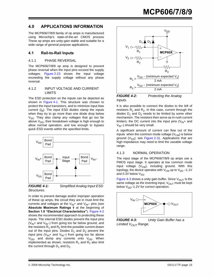
FIGURE 4-1: Simplified Analog Input ESD Structures.In order to prevent damage and/or improper operationof these op amps, the circuit they are in must limit thecurrents and voltages at the VIN+ and VIN– pins (seeAbsolute Maximum Ratings † at the beginning ofSection 1.0 “Electrical Characteristics”). Figure 4-2shows the recommended approach to protecting theseinputs. The internal ESD diodes prevent the input pins(VIN+ and VIN–) from going too far below ground, andthe resistors R1 and R2 limit the possible current drawnout of the input pins. Diodes D1 and D2 prevent theinput pins (VIN+ and VIN–) from going too far aboveVDD, and dump any currents onto VDD. Whenimplemented as shown, resistors R1 and R2 also limitthe current through D1 and D2.
FIGURE 4-2: Protecting the Analog Inputs.It is also possible to connect the diodes to the left ofresistors R1 and R2. In this case, current through thediodes D1 and D2 needs to be limited by some othermechanism. The resistors then serve as in-rush currentlimiters; the DC current into the input pins (VIN+ andVIN–) should be very small.
A significant amount of current can flow out of theinputs when the common mode voltage (VCM) is belowground (VSS); see Figure 2-31. Applications that arehigh impedance may need to limit the useable voltagerange.
4.1.3 NORMAL OPERATIONThe input stage of the MCP606/7/8/9 op amps use aPMOS input stage. It operates at low common modeinput voltage (VCM), including ground. WIth thistopology, the device operates with VCM up to VDD –1.1Vand 0.3V below VSS.
Figure 4-3 shows a unity gain buffer. Since VOUT is thesame voltage as the inverting input, VOUT must be keptbelow VDD–1.2V for correct operation.
FIGURE 4-3: Unity Gain Buffer has a Limited VOUT Range.
BondPad
BondPad
BondPad
VDD
VIN+
VSS
InputStage
BondPad
VIN–
V1R1
VDD
D1
R1 >VSS – (minimum expected V1)
2 mA
R2 >VSS – (minimum expected V2)
2 mA
V2R2
D2
R3
MCP60X
VOUT
+
–
VINMCP60X
© 2009 Microchip Technology Inc. DS11177F-page 15

MCP606/7/8/9
4.2 Rail-to-Rail OutputThere are two specifications that describe theoutput-swing capability of the MCP606/7/8/9 family ofop amps. The first specification (Maximum OutputVoltage Swing) defines the absolute maximum swingthat can be achieved under the specified loadconditions. For instance, the output voltage swings towithin 15 mV of the negative rail with a 25 kΩ load toVDD/2. Figure 2-23 shows how the output voltage islimited when the input goes beyond the linear region ofoperation.The second specification that describes the output-swing capability of these amplifiers (Linear OutputVoltage Range) defines the maximum output swing thatcan be achieved while the amplifier still operates in itslinear region. To verify linear operation in this range, thelarge-signal DC Open-Loop Gain (AOL) is measured atpoints inside the supply rails. The measurement mustmeet the specified AOL conditions in the specificationtable.
4.3 Capacitive LoadsDriving large capacitive loads can cause stabilityproblems for voltage-feedback op amps. As the loadcapacitance increases, the feedback loop’s phasemargin decreases and the closed-loop bandwidth isreduced. This produces gain-peaking in the frequencyresponse, with overshoot and ringing in the stepresponse. A unity-gain buffer (G = +1) is the mostsensitive to capacitive loads, though all gains show thesame general behavior.
When driving large capacitive loads with these opamps (e.g., > 60 pF when G = +1), a small seriesresistor at the output (RISO in Figure 4-4) improves thefeedback loop’s phase margin (stability) by making theoutput load resistive at higher frequencies. Thebandwidth will be generally lower than the bandwidthwith no capacitive load.
FIGURE 4-4: Output Resistor, RISO stabilizes large capacitive loads.Figure 4-5 gives recommended RISO values fordifferent capacitive loads and gains. The x-axis is thenormalized load capacitance (CL/GN), where GN is thecircuit’s noise gain. For non-inverting gains, GN and theSignal Gain are equal. For inverting gains, GN is1+|Signal Gain| (e.g., -1 V/V gives GN = +2 V/V).
FIGURE 4-5: Recommended RISO Values for Capacitive Loads.After selecting RISO for your circuit, double-check theresulting frequency response peaking and stepresponse overshoot. Modify RISO’s value until theresponse is reasonable. Bench evaluation and simula-tions with the MCP606/7/8/9 SPICE macro model arehelpful.
4.4 MCP608 Chip Select The MCP608 is a single op amp with Chip Select (CS).When CS is pulled high, the supply current drops to50 nA (typical) and flows through the CS pin to VSS.When this happens, the amplifier output is put into ahigh-impedance state. By pulling CS low, the amplifieris enabled. The CS pin has an internal 5 MΩ (typical)pull-down resistor connected to VSS, so it will go low ifthe CS pins is left floating. Figure 1-1 shows the outputvoltage and supply current response to a CS pulse.
4.5 Supply BypassWith this family of operational amplifiers, the powersupply pin (VDD for single-supply) should have a localbypass capacitor (i.e., 0.01 µF to 0.1 µF) within 2 mmfor good high-frequency performance. It also needs abulk capacitor (i.e., 1 µF or larger) within 100 mm toprovide large, slow currents. This bulk capacitor can beshared with other nearby analog parts.
VIN
RISOVOUT
CL
MCP60X
100
1000
10000
10 100 1000 10000
Normalized Load Capacitance; CL/GN (F)
Rec
omm
ende
d R
ISO (Ω
)
10p 10n1n100p100
10k
1k
GN = +1GN = +2GN ≥ +4
DS11177F-page 16 © 2009 Microchip Technology Inc.

MCP606/7/8/9
4.6 Unused Op AmpsAn unused op amp in a quad package (MCP609)should be configured as shown in Figure 4-6. Thesecircuits prevent the output from toggling and causingcrosstalk. Circuits A sets the op amp at its minimumnoise gain. The resistor divider produces any desiredreference voltage within the output voltage range of theop amp; the op amp buffers that reference voltage.Circuit B uses the minimum number of componentsand operates as a comparator, but it may draw morecurrent.FIGURE 4-6: Unused Op Amps.
4.7 PCB Surface LeakageIn applications where low input bias current is critical,Printed Circuit Board (PCB) surface-leakage effectsneed to be considered. Surface leakage is caused byhumidity, dust or other contamination on the board.Under low humidity conditions, a typical resistancebetween nearby traces is 1012Ω. A 5V difference wouldcause 5 pA of current to flow, which is greater than theMCP606/7/8/9 family’s bias current at +25°C (1 pA,typical).
The easiest way to reduce surface leakage is to use aguard ring around sensitive pins (or traces). The guardring is biased at the same voltage as the sensitive pin.An example of this type of layout is shown in Figure 4-7.
FIGURE 4-7: Example Guard Ring Layout for Inverting Gain.
1. Non-inverting Gain and Unity-gain Buffer:a) Connect the non-inverting pin (VIN+) to the
input with a wire that does not touch thePCB surface.
b) Connect the guard ring to the inverting inputpin (VIN–). This biases the guard ring to thecommon mode input voltage.
2. Inverting Gain and Transimpedance Gain(convert current to voltage, such as photodetectors) amplifiers:a) Connect the guard ring to the non-inverting
input pin (VIN+). This biases the guard ringto the same reference voltage as the opamp (e.g., VDD/2 or ground).
b) Connect the inverting pin (VIN–) to the inputwith a wire that does not touch the PCBsurface.
4.8 Application Circuits
4.8.1 LOW-SIDE BATTERY CURRENT SENSOR
The MCP606/7/8/9 op amps can be used to sense theload current on the low-side of a battery using thecircuit in Figure 4-8. In this circuit, the current from thepower supply (minus the current required to power theMCP606) flows through a sense resistor (RSEN), whichconverts it to voltage. This is gained by the the amplifierand resistors, RG and RF. Since the non-inverting inputof the amplifier is at the load’s negative supply (VLM),the gain from RSEN to VOUT is RF/RG.
FIGURE 4-8: Low Side Battery Current Sensor.Since the input bias current and input offset voltage ofthe MCP606 are low, and the input is capable ofswinging below ground, there is very little errorgenerated by the amplifier. The quiescent current isvery low, which helps conserve battery power. Therail-to-rail output makes it possible to read very lowcurrents.
VDD
VDD
R1
R2
VDD
VREF
VREF VDDR2
R1 R2+-------------------⋅=
¼ MCP609 (A) ¼ MCP609 (B)
Guard Ring
VSSVIN- VIN+
VOUT VLM I+ LRSEN RF RG⁄( )=
RF
To Load
2.5V
RG5 kΩ 50 kΩ
To Load
VOUT
RSEN10Ω (VLM)
(VLP)
IL
to6.0V
MCP606
© 2009 Microchip Technology Inc. DS11177F-page 17

MCP606/7/8/9
4.8.2 PHOTODIODE AMPLIFIERSSensors that produce an output current and have highoutput impedance can be connected to atransimpedance amplifier. The transimpedanceamplifier converts the current into voltage. Photodiodesare one sensor that produce an output current.The key op amp characteristics that are needed forthese circuits are: low input offset voltage, low inputbias current, high input impedance and an inputcommon mode range that includes ground. The lowinput offset voltage and low input bias current supporta very low voltage drop across the photodiode; thisgives the best photodiode linearity. Since thephotodiode is biased at ground, the op amp’s inputneeds to function well both above and below ground.
4.8.2.1 Photo-Voltaic ModeFigure 4-9 shows a transimpedance amplifier with aphotodiode (D1) biased in the Photo-voltaic mode (0Vacross D1), which is used for precision photodiodesensing.
As light impinges on D1, charge is generated, causinga current to flow in the reverse bias direction of D1. Theop amp’s negative feedback forces the voltage acrossthe D1 to be nearly 0V. Resistor R2 converts the currentinto voltage. Capacitor C2 limits the bandwidth andhelps stabilize the circuit when D1’s junctioncapacitance is large.
FIGURE 4-9: Photodiode (in Photo-voltaic mode) and Transimpedance Amplifier.
4.8.2.2 Photo-Conductive ModeFigure 4-9 shows a transimpedance amplifier with aphotodiode (D1) biased in the Photo-conductive mode(D1 is reverse biased), which is used for high-speedapplications.
As light impinges on D1, charge is generated, causinga current to flow in the reverse bias direction of D1.Placing a negative bias on D1 significantly reduces itsjunction capacitance, which allows the circuit to
operate at a much higher speed. This reverse bias alsoincreases the dark current and current noise, however.Resistor R2 converts the current into voltage. CapacitorC2 limits the bandwidth and helps stabilize the circuitwhen D1’s junction capacitance is large.
FIGURE 4-10: Photodiode (in Photo-conductive mode) and Transimpedance Amplifier.
4.8.3 TWO OP AMP INSTRUMENTATION AMPLIFIER
The two op amp instrumentation amplifier shown inFigure 4-11 serves the function of taking the differenceof two input voltages, level-shifting it and gaining it tothe output. This configuration is best suited for highergains (i.e., gain > 3 V/V). The reference voltage (VREF)is typically at mid-supply (VDD/2) in a single-supplyenvironment.
FIGURE 4-11: Two Op Amp Instrumentation Amplifier.The key specifications that make the MCP606/7/8/9family appropriate for this application circuit are lowinput bias current, low offset voltage and highcommon-mode rejection.
VOUT ID1R2=
R2
D1
VOUT
Light
C2
VDDID1
MCP606
VOUT ID1R2=
R2
D1
VOUT
Light
C2
VDDID1
VB
VB 0<
MCP606
VOUT V1 V2–( ) 1R1R2------
2R1RG----------+ +
⎝ ⎠⎜ ⎟⎛ ⎞
VREF+=
R2R1VOUT
V2
VREF
R1R2
V1
RG
½ MCP607
½ MCP607
DS11177F-page 18 © 2009 Microchip Technology Inc.

MCP606/7/8/9
4.8.4 THREE OP AMPINSTRUMENTATION AMPLIFIERA classic, three op amp instrumentation amplifier isillustrated in Figure 4-12. The two input op ampsprovide differential signal gain and a common modegain of +1. The output op amp is a difference amplifier,which converts its input signal from differential to a sin-gle ended output; it rejects common mode signals at itsinput. The gain of this circuit is simply adjusted with oneresistor (RG). The reference voltage (VREF) is typicallyreferenced to mid-supply (VDD/2) in single-supplyapplications.
FIGURE 4-12: Three Op Amp Instrumentation Amplifier.
4.8.5 PRECISION GAIN WITH GOOD LOAD ISOLATION
In Figure 4-13, the MCP606 op amps, R1 and R2provide a high gain to the input signal (VIN). TheMCP606’s low offset voltage makes this an accuratecircuit.
The MCP601 is configured as a unity-gain buffer. Itisolates the MCP606’s output from the load, increasingthe high-gain stage’s precision. Since the MCP601 hasa higher output current, with the two amplifiers beinghoused in separate packages, there is minimal changein the MCP606’s offset voltage due to loading effect.
FIGURE 4-13: Precision Gain with Good Load Isolation.
VOUT V1 V2–( ) 12R2RG---------+
⎝ ⎠⎜ ⎟⎛ ⎞ R4
R3------
⎝ ⎠⎜ ⎟⎛ ⎞
VREF+=
R2VREF
V1
R4R3
R2
RG
VOUT
V2
R4R3
½ MCP607
½ MCP607
MCP606
VOUT VIN 1 R2 R1⁄+( )=
R2R1
VOUT
VIN MCP601MCP606
© 2009 Microchip Technology Inc. DS11177F-page 19

MCP606/7/8/9
NOTES:DS11177F-page 20 © 2009 Microchip Technology Inc.

MCP606/7/8/9
5.0 DESIGN AIDSMicrochip provides the basic design tools needed forthe MCP606/7/8/9 family of op amps.
5.1 SPICE Macro ModelThe latest SPICE macro model for the MCP606/7/8/9op amps is available on the Microchip web site atwww.microchip.com. This model is intended to be aninitial design tool that works well in the op amp’s linearregion of operation over the temperature range. Seethe model file for information on its capabilities.
Bench testing is a very important part of any design andcannot be replaced with simulations. Also, simulationresults using this macro model need to be validated bycomparing them to the data sheet specifications andcharacteristic curves.
5.2 FilterLab® SoftwareMicrochip’s FilterLab® software is an innovativesoftware tool that simplifies analog active filter (usingop amps) design. Available at no cost from theMicrochip web site at www.microchip.com/filterlab, theFilterLab design tool provides full schematic diagramsof the filter circuit with component values. It alsooutputs the filter circuit in SPICE format, which can beused with the macro model to simulate actual filterperformance.
5.3 Mindi™ Circuit Designer & Simulator
Microchip’s Mindi™ Circuit Designer & Simulator aidsin the design of various circuits useful for active filter,amplifier and power-management applications. It is afree online circuit designer & simulator available fromthe Microchip web site at www.microchip.com/mindi.This interactive circuit designer & simulator enablesdesigners to quickly generate circuit diagrams,simulate circuits. Circuits developed using the MindiCircuit Designer & Simulator can be downloaded to apersonal computer or workstation.
5.4 Microchip Advanced Part Selector (MAPS)
MAPS is a software tool that helps semiconductorprofessionals efficiently identify Microchip devices thatfit a particular design requirement. Available at no costfrom the Microchip website at www.microchip.com/maps, the MAPS is an overall selection tool forMicrochip’s product portfolio that includes Analog,Memory, MCUs and DSCs. Using this tool you candefine a filter to sort features for a parametric search ofdevices and export side-by-side technical comparasionreports. Helpful links are also provided for Datasheets,Purchase, and Sampling of Microchip parts.
5.5 Analog Demonstration and Evaluation Boards
Microchip offers a broad spectrum of AnalogDemonstration and Evaluation Boards that aredesigned to help you achieve faster time to market. Fora complete listing of these boards and theircorresponding user’s guides and technical information,visit the Microchip web site at www.microchip.com/analogtools.
Two of our boards that are especially useful are:
• 8-Pin SOIC/MSOP/TSSOP/DIP Evaluation Board, P/N SOIC8EV
• 14-Pin SOIC/TSSOP/DIP Evaluation Board, P/N SOIC14EV
5.6 Application NotesThe following Microchip Application Notes are avail-able on the Microchip web site at www.microchip. com/appnotes and are recommended as supplementalreference resources.
• ADN003: “Select the Right Operational Amplifier for your Filtering Circuits”, DS21821
• AN722: “Operational Amplifier Topologies and DC Specifications”, DS00722
• AN723: “Operational Amplifier AC Specifications and Applications”, DS00723
• AN884: “Driving Capacitive Loads With Op Amps”, DS00884
• AN990: “Analog Sensor Conditioning Circuits –An Overview”, DS00990
These application notes and others are listed in thedesign guide:
“Signal Chain Design Guide”, DS21825
© 2009 Microchip Technology Inc. DS11177F-page 21

MCP606/7/8/9
NOTES:DS11177F-page 22 © 2009 Microchip Technology Inc.

MCP606/7/8/9
6.0 PACKAGING INFORMATION
6.1 Package Marking Information
Legend: XX...X Customer-specific informationY Year code (last digit of calendar year)YY Year code (last 2 digits of calendar year)WW Week code (week of January 1 is week ‘01’)NNN Alphanumeric traceability code Pb-free JEDEC designator for Matte Tin (Sn)* This package is Pb-free. The Pb-free JEDEC designator ( )
can be found on the outer packaging for this package.
Note: In the event the full Microchip part number cannot be marked on one line, it willbe carried over to the next line, thus limiting the number of availablecharacters for customer-specific information.
3e
3e
5-Lead SOT-23 (MCP606) Example:
XXNN SB25
XXXXXXXXXXXXXNNN
YYWW
8-Lead PDIP (300 mil) Example:
8-Lead SOIC (150 mil) Example:
XXXXXXXXXXXXYYWW
NNN
MCP606I/P256
0722
MCP606I/SN0722
256
MCP606I/P 256
0936
MCP606ISN 0936
256
3eOR
OR 3e
8-Lead TSSOP Example:
XXXX
YYWW
NNN
606
I936
256
© 2009 Microchip Technology Inc. DS11177F-page 23

MCP606/7/8/9
Package Marking Information (Continued)14-Lead TSSOP (MCP609) Example:
XXXXXXXXYYWW
NNN
609IST0936
256
14-Lead PDIP (300 mil) (MCP609) Example:
XXXXXXXXXXXXXXXXXXXXXXXXXXXX
YYWWNNN
MCP609-I/P
0722256
MCP609
0936256I/P 3eOR
14-Lead SOIC (150 mil) (MCP609) Example:
XXXXXXXXXX
YYWWNNNXXXXXXXXXX
MCP609ISL
0722256
MCP609
0936256I/SL^^OR 3e
DS11177F-page 24 © 2009 Microchip Technology Inc.

MCP606/7/8/9
!"!#$! !% #$ !% #$ # & ! ! !# "'(
)*+ ) # &#,$ --#$##
.# #$ #/ !- 0 # 1/ %## !###+22---2/
3# 44"" 4# 5 56 7
5$8 %1 5 (4 !1# ()*6$# ! 4 !1# )*6, 9 # : (! !1/ / ; : #!%% : (6, <!# " : ! !1/ <!# " : ;6, 4 # : .#4 # 4 : =.## 4 ( : ;.# > : >4 !/ ; : =4 !<!# 8 : (
φ
Nb
E
E1
D
1 2 3
e
e1
A
A1
A2 c
L
L1
- *)
© 2009 Microchip Technology Inc. DS11177F-page 25

MCP606/7/8/9
! "## $% !
1, $! &% #$ ,08$#$ #8 # !-## # ! ?%#*# # !"!#$! !% #$ !% #$ # & !@ ! !# "'(
)*+) # &#,$ --#$##
.# #$ #/ !- 0 # 1/ %## !###+22---2/
3# 5*9" 4# 5 56 7
5$8 %1 5 ;1# )*# #1 : : ! !1/ / ( () # #1 ( : :$! #$! <!# " (! !1/ <!# " ( ;6, 4 # ; =( # #1 4 ( (4 !/ ; (3 4 !<!# 8 = 4- 4 !<!# 8 ; 6, -? ) : :
N
E1
NOTE 1
D
1 2 3
A
A1
A2
L
b1b
e
E
eB
c
- *;)
DS11177F-page 26 © 2009 Microchip Technology Inc.

MCP606/7/8/9
"&'()#$%!*
1, $! &% #$ ,08$#$ #8 # !-## # ! ?%#*# # !"!#$! !% #$ !% #$ # & !( ! !# "'(
)*+ ) # &#,$ --#$## ".+ % 0$ $-#$## 0%%#$
.# #$ #/ !- 0 # 1/ %## !###+22---2/
3# 44"" 4# 5 56 7
5$8 %1 5 ;1# )*6, 9 # : : (! !1/ / ( : :#!%%? : (6, <!# " =)*! !1/ <!# " )*6, 4 # )**% A#B ( : (.#4 # 4 : .## 4 "..# > : ;>4 !/ : (4 !<!# 8 : (!%# (> : (>!%# )## (> : (>
D
Ne
E
E1
NOTE 1
1 2 3
b
A
A1
A2
L
L1
c
h
h
φ
β
α
- *()
© 2009 Microchip Technology Inc. DS11177F-page 27

MCP606/7/8/9
"&'()#$%!*
.# #$ #/ !- 0 # 1/ %## !###+22---2/
DS11177F-page 28 © 2009 Microchip Technology Inc.

MCP606/7/8/9
+ + , "-(-$%
1, $! &% #$ ,08$#$ #8 # !-## # ! !"!#$! !% #$ !% #$ # & !( ! !# "'(
)*+ ) # &#,$ --#$## ".+ % 0$ $-#$## 0%%#$
.# #$ #/ !- 0 # 1/ %## !###+22---2/
3# 44"" 4# 5 56 7
5$8 %1 5 ;1# =()*6, 9 # : : ! !1/ / ; (#!%% ( : (6, <!# " =)*! !1/ <!# " (! !1/ 4 # .#4 # 4 ( = (.## 4 "..# > : ;>4 !/ : 4 !<!# 8 :
D
N
E
E1
NOTE 1
1 2
be
cA
A1
A2
L1 L
φ
- *;=)
© 2009 Microchip Technology Inc. DS11177F-page 29

MCP606/7/8/9
Note: For the most current package drawings, please see the Microchip Packaging Specification located at http://www.microchip.com/packaging
DS11177F-page 30 © 2009 Microchip Technology Inc.

MCP606/7/8/9
.- ! "## $% !
1, $! &% #$ ,08$#$ #8 # !-## # ! ?%#*# # !"!#$! !% #$ !% #$ # & !@ ! !# "'(
)*+) # &#,$ --#$##
.# #$ #/ !- 0 # 1/ %## !###+22---2/
3# 5*9" 4# 5 56 7
5$8 %1 5 1# )*# #1 : : ! !1/ / ( () # #1 ( : :$! #$! <!# " (! !1/ <!# " ( ;6, 4 # ( ( (# #1 4 ( (4 !/ ; (3 4 !<!# 8 ( = 4- 4 !<!# 8 ; 6, -? ) : :
N
E1
D
NOTE 1
1 2 3
E
c
eB
A2
L
A
A1b1
b e
- *()
© 2009 Microchip Technology Inc. DS11177F-page 31

MCP606/7/8/9
.- "&'()#$%!*
1, $! &% #$ ,08$#$ #8 # !-## # ! ?%#*# # !"!#$! !% #$ !% #$ # & !( ! !# "'(
)*+ ) # &#,$ --#$## ".+ % 0$ $-#$## 0%%#$
.# #$ #/ !- 0 # 1/ %## !###+22---2/
3# 44"" 4# 5 56 7
5$8 %1 5 1# )*6, 9 # : : (! !1/ / ( : :#!%%? : (6, <!# " =)*! !1/ <!# " )*6, 4 # ;=()**% A#B ( : (.#4 # 4 : .## 4 "..# > : ;>4 !/ : (4 !<!# 8 : (!%# (> : (>!%# )## (> : (>
NOTE 1
N
D
E
E1
1 2 3
b
e
A
A1
A2
L
L1
c
h
h α
β
φ
- *=()
DS11177F-page 32 © 2009 Microchip Technology Inc.
MCP606/7/8/9
.# #$ #/ !- 0 # 1/ %## !###+22---2/
© 2009 Microchip Technology Inc. DS11177F-page 33

MCP606/7/8/9
.- + + , "-(-$%
1, $! &% #$ ,08$#$ #8 # !-## # ! !"!#$! !% #$ !% #$ # & !( ! !# "'(
)*+ ) # &#,$ --#$## ".+ % 0$ $-#$## 0%%#$
.# #$ #/ !- 0 # 1/ %## !###+22---2/
3# 44"" 4# 5 56 7
5$8 %1 5 1# =()*6, 9 # : : ! !1/ / ; (#!%% ( : (6, <!# " =)*! !1/ <!# " (! !1/ 4 # ( (.#4 # 4 ( = (.## 4 "..# > : ;>4 !/ : 4 !<!# 8 :
NOTE 1
D
N
E
E1
1 2
eb
cA
A1
A2
L1 L
φ
- *;)
DS11177F-page 34 © 2009 Microchip Technology Inc.

MCP606/7/8/9
Note: For the most current package drawings, please see the Microchip Packaging Specification located at http://www.microchip.com/packaging
© 2009 Microchip Technology Inc. DS11177F-page 35

MCP606/7/8/9
NOTES:DS11177F-page 36 © 2009 Microchip Technology Inc.

MCP606/7/8/9
APPENDIX A: REVISION HISTORY
Revision F (September 2009)The following is the list of modifications:
1. Corrected RL text in Figure 2-22 in Section 2.0“Typical Performance Curves”.
2. Corrected devices’ pins in Table 3-1(Section 3.0 “Pin Descriptions”).
3. Updated Section 6.0 “Packaging Informa-tion”. Updated package outline drawings.
Revision E (March 2008)The following is the list of modifications:
1. Increased maximum operating VDD.2. Added test circuits.3. Updated performance curves.4. Added Figure 2-31.5. Added Section 4.1.1 “Phase Reversal”,
Section 4.1.2 “Input Voltage and CurrentLimits”, ad Section 4.1.3 “Normal Opera-tion”.
6. Updated Section 5.0 “Design Aids”7. Updated Section 6.0 “Packaging Informa-
tion”. Updated package outline drawings.
Revision D (February 2005)The following is the list of modifications:
1. Added Section 3.0 “Pin Descriptions”.2. Updated Section 4.0 “Applications Information”.3. Added Section 4.3 “Capacitive Loads”4. Updated Section 5.0 “Design Aids” to include
FilterLab® and to point to the latest SPICEmacro model.
5. Corrected and updated Section 6.0 “PackagingInformation”.
6. Added Appendix A: “Revision History”.
Revision C (January 2001)• Undocumented changes
Revision B (May 2000)• Undocumented changes
Revision A (January 2000)• Original Release of this Document.
© 2009 Microchip Technology Inc. DS11177F-page 37

MCP606/7/8/9
NOTES:DS11177F-page 38 © 2009 Microchip Technology Inc.
MCP606/7/8/9
PRODUCT IDENTIFICATION SYSTEMTo order or obtain information, e.g., on pricing or delivery, refer to the factory or the listed sales office.
Device MCP606 = Single Op AmpMCP606T = Single Op Amp
Tape and Reel (SOIC, TSSOP)MCP607 = Dual Op AmpMCP607T = Dual Op Amp
Tape and Reel (SOIC, TSSOP)MCP608 = Single Op Amp with CSMCP608T = Single Op Amp with CS
Tape and Reel (SOIC, TSSOP)MCP609 = Quad Op AmpMCP609T = Quad Op Amp
Tape and Reel (SOIC, TSSOP)
Temperature Range I = -40°C to +85°C
Package OT = Plastic SOT-23, 5-leadP = Plastic DIP (300 mil Body), 8-lead, 14-leadSN = Plastic SOIC (3.90 mm body), 8-leadSL = Plastic SOIC (3.90 mm body), 14-leadST = Plastic TSSOP, 8-lead, 14-lead
Examples:a) MCP606-I/P: Industrial Temperature,
8LD PDIP package.b) MCP606-I/SN: Industrial Temperature,
8LD SOIC package.c) MCP606T-I/SN: Tape and Reel,
Industrial Temperature,8LD SOIC package.
d) MCP606-I/ST: Industrial Temperature,8LD TSSOP package.
e) MCP606T-I/OT: Tape and Reel,Industrial Temperature,5LD SOT-23 package.
a) MCP607-I/P: Industrial Temperature,8LD PDIP package.
b) MCP607T-I/SN: Tape and Reel,Industrial Temperature,8LD SOIC package.
a) MCP608-I/SN: Industrial Temperature,8LD SOIC package.
b) MCP608T-I/SN: Tape and Reel,Industrial Temperature,8LD SOIC package.
a) MCP609-I/P: Industrial Temperature,14LD PDIP package.
b) MCP609T-I/SL: Tape and Reel, Industrial Temperature,14LD SOIC package.
PART NO. X /XX
PackageTemperatureRange
Device
© 2009 Microchip Technology Inc. DS11177F-page 39

MCP606/7/8/9
NOTES:DS11177F-page 40 © 2009 Microchip Technology Inc.
Note the following details of the code protection feature on Microchip devices:• Microchip products meet the specification contained in their particular Microchip Data Sheet.
• Microchip believes that its family of products is one of the most secure families of its kind on the market today, when used in the intended manner and under normal conditions.
• There are dishonest and possibly illegal methods used to breach the code protection feature. All of these methods, to our knowledge, require using the Microchip products in a manner outside the operating specifications contained in Microchip’s Data Sheets. Most likely, the person doing so is engaged in theft of intellectual property.
• Microchip is willing to work with the customer who is concerned about the integrity of their code.
• Neither Microchip nor any other semiconductor manufacturer can guarantee the security of their code. Code protection does not mean that we are guaranteeing the product as “unbreakable.”
Code protection is constantly evolving. We at Microchip are committed to continuously improving the code protection features of ourproducts. Attempts to break Microchip’s code protection feature may be a violation of the Digital Millennium Copyright Act. If such actsallow unauthorized access to your software or other copyrighted work, you may have a right to sue for relief under that Act.
Information contained in this publication regarding deviceapplications and the like is provided only for your convenienceand may be superseded by updates. It is your responsibility toensure that your application meets with your specifications.MICROCHIP MAKES NO REPRESENTATIONS ORWARRANTIES OF ANY KIND WHETHER EXPRESS ORIMPLIED, WRITTEN OR ORAL, STATUTORY OROTHERWISE, RELATED TO THE INFORMATION,INCLUDING BUT NOT LIMITED TO ITS CONDITION,QUALITY, PERFORMANCE, MERCHANTABILITY ORFITNESS FOR PURPOSE. Microchip disclaims all liabilityarising from this information and its use. Use of Microchipdevices in life support and/or safety applications is entirely atthe buyer’s risk, and the buyer agrees to defend, indemnify andhold harmless Microchip from any and all damages, claims,suits, or expenses resulting from such use. No licenses areconveyed, implicitly or otherwise, under any Microchipintellectual property rights.
© 2009 Microchip Technology Inc.
Trademarks
The Microchip name and logo, the Microchip logo, dsPIC, KEELOQ, KEELOQ logo, MPLAB, PIC, PICmicro, PICSTART, rfPIC and UNI/O are registered trademarks of Microchip Technology Incorporated in the U.S.A. and other countries.
FilterLab, Hampshire, HI-TECH C, Linear Active Thermistor, MXDEV, MXLAB, SEEVAL and The Embedded Control Solutions Company are registered trademarks of Microchip Technology Incorporated in the U.S.A.
Analog-for-the-Digital Age, Application Maestro, CodeGuard, dsPICDEM, dsPICDEM.net, dsPICworks, dsSPEAK, ECAN, ECONOMONITOR, FanSense, HI-TIDE, In-Circuit Serial Programming, ICSP, Mindi, MiWi, MPASM, MPLAB Certified logo, MPLIB, MPLINK, mTouch, Octopus, Omniscient Code Generation, PICC, PICC-18, PICDEM, PICDEM.net, PICkit, PICtail, PIC32 logo, REAL ICE, rfLAB, Select Mode, Total Endurance, TSHARC, UniWinDriver, WiperLock and ZENA are trademarks of Microchip Technology Incorporated in the U.S.A. and other countries.
SQTP is a service mark of Microchip Technology Incorporated in the U.S.A.
All other trademarks mentioned herein are property of their respective companies.
© 2009, Microchip Technology Incorporated, Printed in the U.S.A., All Rights Reserved.
Printed on recycled paper.
DS11177F-page 41
Microchip received ISO/TS-16949:2002 certification for its worldwide headquarters, design and wafer fabrication facilities in Chandler and Tempe, Arizona; Gresham, Oregon and design centers in California and India. The Company’s quality system processes and procedures are for its PIC® MCUs and dsPIC® DSCs, KEELOQ® code hopping devices, Serial EEPROMs, microperipherals, nonvolatile memory and analog products. In addition, Microchip’s quality system for the design and manufacture of development systems is ISO 9001:2000 certified.

DS11177F-page 42 © 2009 Microchip Technology Inc.
AMERICASCorporate Office2355 West Chandler Blvd.Chandler, AZ 85224-6199Tel: 480-792-7200 Fax: 480-792-7277Technical Support: http://support.microchip.comWeb Address: www.microchip.comAtlantaDuluth, GA Tel: 678-957-9614 Fax: 678-957-1455BostonWestborough, MA Tel: 774-760-0087 Fax: 774-760-0088ChicagoItasca, IL Tel: 630-285-0071 Fax: 630-285-0075ClevelandIndependence, OH Tel: 216-447-0464 Fax: 216-447-0643DallasAddison, TX Tel: 972-818-7423 Fax: 972-818-2924DetroitFarmington Hills, MI Tel: 248-538-2250Fax: 248-538-2260KokomoKokomo, IN Tel: 765-864-8360Fax: 765-864-8387Los AngelesMission Viejo, CA Tel: 949-462-9523 Fax: 949-462-9608Santa ClaraSanta Clara, CA Tel: 408-961-6444Fax: 408-961-6445TorontoMississauga, Ontario, CanadaTel: 905-673-0699 Fax: 905-673-6509
ASIA/PACIFICAsia Pacific OfficeSuites 3707-14, 37th FloorTower 6, The GatewayHarbour City, KowloonHong KongTel: 852-2401-1200Fax: 852-2401-3431Australia - SydneyTel: 61-2-9868-6733Fax: 61-2-9868-6755China - BeijingTel: 86-10-8528-2100 Fax: 86-10-8528-2104China - ChengduTel: 86-28-8665-5511Fax: 86-28-8665-7889China - Hong Kong SARTel: 852-2401-1200 Fax: 852-2401-3431China - NanjingTel: 86-25-8473-2460Fax: 86-25-8473-2470China - QingdaoTel: 86-532-8502-7355Fax: 86-532-8502-7205China - ShanghaiTel: 86-21-5407-5533 Fax: 86-21-5407-5066China - ShenyangTel: 86-24-2334-2829Fax: 86-24-2334-2393China - ShenzhenTel: 86-755-8203-2660 Fax: 86-755-8203-1760China - WuhanTel: 86-27-5980-5300Fax: 86-27-5980-5118China - XiamenTel: 86-592-2388138 Fax: 86-592-2388130China - XianTel: 86-29-8833-7252Fax: 86-29-8833-7256China - ZhuhaiTel: 86-756-3210040 Fax: 86-756-3210049
ASIA/PACIFICIndia - BangaloreTel: 91-80-3090-4444 Fax: 91-80-3090-4080India - New DelhiTel: 91-11-4160-8631Fax: 91-11-4160-8632India - PuneTel: 91-20-2566-1512Fax: 91-20-2566-1513Japan - YokohamaTel: 81-45-471- 6166 Fax: 81-45-471-6122Korea - DaeguTel: 82-53-744-4301Fax: 82-53-744-4302Korea - SeoulTel: 82-2-554-7200Fax: 82-2-558-5932 or 82-2-558-5934Malaysia - Kuala LumpurTel: 60-3-6201-9857Fax: 60-3-6201-9859Malaysia - PenangTel: 60-4-227-8870Fax: 60-4-227-4068Philippines - ManilaTel: 63-2-634-9065Fax: 63-2-634-9069SingaporeTel: 65-6334-8870Fax: 65-6334-8850Taiwan - Hsin ChuTel: 886-3-6578-300Fax: 886-3-6578-370Taiwan - KaohsiungTel: 886-7-536-4818Fax: 886-7-536-4803Taiwan - TaipeiTel: 886-2-2500-6610 Fax: 886-2-2508-0102Thailand - BangkokTel: 66-2-694-1351Fax: 66-2-694-1350
EUROPEAustria - WelsTel: 43-7242-2244-39Fax: 43-7242-2244-393Denmark - CopenhagenTel: 45-4450-2828 Fax: 45-4485-2829France - ParisTel: 33-1-69-53-63-20 Fax: 33-1-69-30-90-79Germany - MunichTel: 49-89-627-144-0 Fax: 49-89-627-144-44Italy - Milan Tel: 39-0331-742611 Fax: 39-0331-466781Netherlands - DrunenTel: 31-416-690399 Fax: 31-416-690340Spain - MadridTel: 34-91-708-08-90Fax: 34-91-708-08-91UK - WokinghamTel: 44-118-921-5869Fax: 44-118-921-5820
WORLDWIDE SALES AND SERVICE
03/26/09