23.solved paper gate (ec) by kanodia
TRANSCRIPT

GATEELECTRONICS & COMMUNICATION
Solved Paper ( 2013-1996 )
RK Kanodia Ashish Murolia
For GATE 2014 All session paper visit
www.nodia.co.in
NODIA & COMPANY

For Best Test Series Visit
www.gatehelp.comReal IIT Exam Environment
GATE Electronics & CommunicationSolved Paper (2013 - 1996 )RK Kanodia & Ashish Murolia
Copyright © By NODIA & COMPANY
Information contained in this book has been obtained by author, from sources believes to be reliable. However, neither NODIA & COMPANY nor its author guarantee the accuracy or completeness of any information herein, and NODIA & COMPANY nor its author shall be responsible for any error, omissions, or damages arising out of use of this information. This book is published with the understanding that NODIA & COMPANY and its author
are supplying information but are not attempting to render engineering or other professional services.
NODIA & COMPANYB 8, Dhanshree Ist, Central Spine, Vidyadhar Nagar, Jaipur 302039Ph : +91 141 2101150, www.nodia.co.inemail : [email protected]
Printed by Nodia and Company, Jaipur

SYLLABUS
GENERAL ABILITY
Verbal Ability : English grammar, sentence completion, verbal analogies, word groups, instructions, critical reasoning and verbal deduction.
Numerical Ability : Numerical computation, numerical estimation, numerical reasoning and data interpretation.
ENGINEERING MATHEMATICS
Linear Algebra: Matrix Algebra, Systems of linear equations, Eigen values and eigen vectors.
Calculus : Mean value theorems, Theorems of integral calculus, Evaluation of definite and improper integrals, Partial Derivatives, Maxima and minima, Multiple integrals, Fourier series. Vector identities, Directional derivatives, Line, Surface and Volume integrals, Stokes, Gauss and Green’s theorems.
Differential equations : First order equation (linear and nonlinear), Higher order linear differential equations with constant coefficients, Method of variation of parameters, Cauchy’s and Euler’s equations, Initial and boundary value problems, Partial Differential Equations and variable separable method.
Complex variables : Analytic functions, Cauchy’s integral theorem and integral formula, Taylor’s and Laurent’ series, Residue theorem, solution integrals.
Probability and Statistics : Sampling theorems, Conditional probability, Mean, median, mode and standard deviation, Random variables, Discrete and continuous distributions, Poisson, Normal and Binomial distribution, Correlation and regression analysis.
Numerical Methods : Solutions of non-linear algebraic equations, single and multi-step methods for differential equations.
Transform Theory : Fourier transform, Laplace transform, Z-transform.
Electronics and Communication Engineering
Networks : Network graphs: matrices associated with graphs; incidence, fundamental cut set and fundamental circuit matrices. Solution methods: nodal and mesh analysis. Network theorems: superposition, Thevenin and Norton’s maximum power transfer, Wye-Delta transformation. Steady state sinusoidal analysis using phasors. Linear constant coefficient differential equations; time domain analysis of simple RLC circuits, Solution of network equations using Laplace transform: frequency domain analysis of RLC circuits. 2-port network parameters: driving point and transfer functions. State equations for networks.
Electronic Devices : Energy bands in silicon, intrinsic and extrinsic silicon. Carrier transport in silicon: diffusion current, drift current, mobility, and resistivity. Generation and recombination of carriers. p-n junction diode, Zener diode, tunnel diode, BJT, JFET, MOS capacitor, MOSFET, LED, p-I-n and avalanche photo diode, Basics of LASERs. Device technology: integrated circuits fabrication process, oxidation, diffusion, ion implantation, photolithography,

n-tub, p-tub and twin-tub CMOS process.
Analog Circuits : Small Signal Equivalent circuits of diodes, BJTs, MOSFETs and analog CMOS. Simple diode circuits, clipping, clamping, rectifier. Biasing and bias stability of transistor and FET amplifiers. Amplifiers: single-and multi-stage, differential and operational, feedback, and power. Frequency response of amplifiers. Simple op-amp circuits. Filters. Sinusoidal oscillators; criterion for oscillation; single-transistor and op-amp configurations. Function generators and wave-shaping circuits, 555 Timers. Power supplies.
Digital circuits : Boolean algebra, minimization of Boolean functions; logic gates; digital IC families (DTL, TTL, ECL, MOS, CMOS). Combinatorial circuits: arithmetic circuits, code converters, multiplexers, decoders, PROMs and PLAs. Sequential circuits: latches and flip-flops, counters and shift-registers. Sample and hold circuits, ADCs, DACs. Semiconductor memories. Microprocessor(8085): architecture, programming, memory and I/O interfacing.
Signals and Systems : Definitions and properties of Laplace transform, continuous-time and discrete-time Fourier series, continuous-time and discrete-time Fourier Transform, DFT and FFT, z-transform. Sampling theorem. Linear Time-Invariant (LTI) Systems: definitions and properties; causality, stability, impulse response, convolution, poles and zeros, parallel and cascade structure, frequency response, group delay, phase delay. Signal transmission through LTI systems.
Control Systems : Basic control system components; block diagrammatic description, reduction of block diagrams. Open loop and closed loop (feedback) systems and stability analysis of these systems. Signal flow graphs and their use in determining transfer functions of systems; transient and steady state analysis of LTI control systems and frequency response. Tools and techniques for LTI control system analysis: root loci, Routh-Hurwitz criterion, Bode and Nyquist plots. Control system compensators: elements of lead and lag compensation, elements of Proportional-Integral-Derivative (PID) control. State variable representation and solution of state equation of LTI control systems.
Communications : Random signals and noise: probability, random variables, probability density function, autocorrelation, power spectral density. Analog communication systems: amplitude and angle modulation and demodulation systems, spectral analysis of these operations, superheterodyne receivers; elements of hardware, realizations of analog communication systems; signal-to-noise ratio (SNR) calculations for amplitude modulation (AM) and frequency modulation (FM) for low noise conditions. Fundamentals of information theory and channel capacity theorem. Digital communication systems: pulse code modulation (PCM), differential pulse code modulation (DPCM), digital modulation schemes: amplitude, phase and frequency shift keying schemes (ASK, PSK, FSK), matched filter receivers, bandwidth consideration and probability of error calculations for these schemes. Basics of TDMA, FDMA and CDMA and GSM.
Electromagnetics : Elements of vector calculus: divergence and curl; Gauss’ and Stokes’ theorems, Maxwell’s equations: differential and integral forms. Wave equation, Poynting vector. Plane waves: propagation through various media; reflection and refraction; phase and group velocity; skin depth. Transmission lines: characteristic impedance; impedance transformation; Smith chart; impedance matching; S parameters, pulse excitation. Waveguides: modes in rectangular waveguides; boundary conditions; cut-off frequencies; dispersion relations. Basics of propagation in dielectric waveguide and optical fibers. Basics of Antennas: Dipole antennas; radiation pattern; antenna gain.
***********

PREFACEThis book doesn’t make promise but provides complete satisfaction to the readers. The market scenario is confusing and readers don’t find the optimum quality books. This book provides complete set of problems appeared in competition exams as well as fresh set of problems.
The book is categorized into units which are then sub-divided into chapters and the concepts of the problems are addressed in the relevant chapters. The aim of the book is to avoid the unnecessary elaboration and highlights only those concepts and techniques which are absolutely necessary. Again time is a critical factor both from the point of view of preparation duration and time taken for solving each problem in the examination. So the problems solving methods is the books are those which take the least distance to the solution.
But however to make a comment that this book is absolute for GATE preparation will be an inappropriate one. The theory for the preparation of the examination should be followed from the standard books. But for a wide collection of problems, for a variety of problems and the efficient way of solving them, what one needs to go needs to go through is there in there in the book. Each unit (e.g. Networks) is subdivided into average seven number of chapters on an average each of which contains 40 problems which are selected so as to avoid unnecessary redundancy and highly needed completeness.
I shall appreciate and greatly acknowledge the comments and suggestion from the users of this book.
R. K. KanodiaAshish Murolia

CONTENTS
CHAP 1 Engineering Mathematics 1 - 31
CHAP 2 Networks 32 - 100
CHAP 3 Electronics Devices 100 - 136
CHAP 4 Analog Circuits 137 - 213
CHAP 5 Digital Circuits 214 - 281
CHAP 6 Signals and Systems 282 - 328
CHAP 7 Control Systems 329 - 385
CHAP 8 Electromagnetic 386 - 435
CHAP 8 Communication Systems 436 - 502
***********

CHAPTER 1ENGINEERING MATHEMATICS
nodia
2013 ONE MARK
MCQ 1.1 The maximum value of q until which the approximation sin .q q holds to within 10% error is(A) 10c (B) 18c
(C) 50c (D) 90c
MCQ 1.2 The minimum eigen value of the following matrix is352
5127
275
R
T
SSSS
V
X
WWWW
(A) 0 (B) 1
(C) 2 (D) 3
MCQ 1.3 A polynomial ( )f x a x a x a x a x a44
33
22
1 0= + + + - with all coefficients positive has(A) no real roots
(B) no negative real root
(C) odd number of real roots
(D) at least one positive and one negative real root
2013 TWO MARKS
MCQ 1.4 Let A be an m n# matrix and B an n m# matrix. It is given that determinant I ABm + =^ h determinant I BAn +^ h, where Ik is the k k# identity matrix. Using
the above property, the determinant of the matrix given below is2111
1211
1121
1112
R
T
SSSSSS
V
X
WWWWWW
(A) 2 (B) 5
(C) 8 (D) 16
2012 ONE MARK
MCQ 1.5 With initial condition ( ) .x 1 0 5= , the solution of the differential equation
t dtdx x t+ = , is
(A) x t 21= - (B) x t 2
12= -
(C) x t22
= (D) x t2=
MCQ 1.6 Given ( )f z z z11
32= + - + .

Page 2 Engineering Mathematics Chapter 1
nodia
Shop GATE Electronics & Communication in 10 Volumes by RK Kanodia at maximum discount at www.nodia.co.in
For online test series visit www.gatehelp.com
If C is a counter clockwise path in the z -plane such that z 1 1+ = , the value
of ( )j f z dz21
Cp # is
(A) 2- (B) 1-(C) 1 (D) 2
MCQ 1.7 If ,x 1= - then the value of xx is(A) e /2p- (B) e /2p
(C) x (D) 1
2012 TWO MARKS
MCQ 1.8 Consider the differential equation
( ) ( )
( )dt
d y tdt
dy ty t22
2
+ + ( )td= with ( ) 2 0andy t dtdy
tt
00
=- ==
=-
-
The numerical value of dtdy
t 0= +
is(A) 2- (B) 1-(C) 0 (D) 1
MCQ 1.9 The direction of vector A is radially outward from the origin, with krA n= . where r x y z2 2 2 2= + + and k is a constant. The value of n for which A 0:d = is(A) 2- (B) 2
(C) 1 (D) 0
MCQ 1.10 A fair coin is tossed till a head appears for the first time. The probability that the number of required tosses is odd, is(A) /1 3 (B) /1 2
(C) /2 3 (D) /3 4
MCQ 1.11 The maximum value of ( )f x x x x9 24 53 2= - + + in the interval [ , ]1 6 is(A) 21 (B) 25
(C) 41 (D) 46
MCQ 1.12 Given that
andA I52
30
10
01=
- -=> >H H, the value of A3 is
(A) 15 12A I+ (B) 19 30A I+(C) 17 15A I+ (D) 17 21A I+
2011 ONE MARK
MCQ 1.13 Consider a closed surface S surrounding volume V . If rv is the position vector of a point inside S , with nt the unit normal on S , the value of the integral r n dS5
S$v t##
is
(A) V3 (B) V5
(C) V10 (D) V15
MCQ 1.14 The solution of the differential equation , (0)dxdy ky y c= = is
(A) x ce ky= - (B) x kecy=

Chapter 1 Engineering Mathematics Page 3
nodia
Shop GATE Electronics & Communication in 10 Volumes by RK Kanodia at maximum discount at www.nodia.co.in
For online test series visit www.gatehelp.com
(C) y cekx= (D) y ce kx= -
MCQ 1.15 The value of the integral ( )z z
z dz4 5
3 4
c2 + +- +# where c is the circle z 1= is given
by(A) 0 (B) 1/10
(C) 4/5 (D) 1
2011 TWO MARKS
MCQ 1.16 A numerical solution of the equation ( )f x x 3 0+ - = can be obtained using Newton- Raphson method. If the starting value is x 2= for the iteration, the value of x that is to be used in the next step is(A) 0.306 (B) 0.739
(C) 1.694 (D) 2.306
MCQ 1.17 The system of equations
4 6 20
4
x y z
x y y
x y z
6
ml
+ + =+ + =+ + =
has NO solution for values of l and μ given by(A) 6, 20ml = = (B) 6, 20ml = =Y(C) 6, 20ml = =Y (D) 6, 20ml = =Y
MCQ 1.18 A fair dice is tossed two times. The probability that the second toss results in a value that is higher than the first toss is(A) 2/36 (B) 2/6
(C) 5/12 (D) 1/2
2010 ONE MARKS
MCQ 1.19 The eigen values of a skew-symmetric matrix are(A) always zero (B) always pure imaginary
(C) either zero or pure imaginary (D) always real
MCQ 1.20 The trigonometric Fourier series for the waveform ( )f t shown below contains
(A) only cosine terms and zero values for the dc components
(B) only cosine terms and a positive value for the dc components
(C) only cosine terms and a negative value for the dc components
(D) only sine terms and a negative value for the dc components

Page 4 Engineering Mathematics Chapter 1
nodia
Shop GATE Electronics & Communication in 10 Volumes by RK Kanodia at maximum discount at www.nodia.co.in
For online test series visit www.gatehelp.com
MCQ 1.21 A function ( )n x satisfied the differential equation ( ) ( )
dxd n x
Ln x
02
2
2- =
where L is a constant. The boundary conditions are : (0)n K= and ( )n 03 = . The solution to this equation is(A) ( ) ( / )expn x K x L= (B) ( ) ( / )expn x K x L= -(C) ( ) ( / )expn x K x L2= - (D) ( ) ( / )expn x K x L= -
2010 TWO MARKS
MCQ 1.22 If e x /y x1= , then y has a(A) maximum at x e= (B) minimum at x e=(C) maximum at x e 1= - (D) minimum at x e 1= -
MCQ 1.23 A fair coin is tossed independently four times. The probability of the event “the number of time heads shown up is more than the number of times tail shown up”(A) 1/16 (B) 1/3
(C) 1/4 (D) 5/16
MCQ 1.24 If A xya x ax y2= +v t t , then A dl
C
$v v# over the path shown in the figure is
(A) 0 (B) 3
2
(C) 1 (D) 2 3
MCQ 1.25 The residues of a complex function
( )( )( )
x zz z z
z1 2
1 2= - --
at its poles are
(A) ,21
21- and 1 (B) ,2
121- and 1-
(C) , 121 and 2
3- (D) ,21 1- and 2
3
MCQ 1.26 Consider differential equation ( )
( )dxdy x
y x x- = , with the initial
condition ( )y 0 0= . Using Euler’s first order method with a step size of 0.1, the value of ( . )y 0 3 is(A) 0.01 (B) 0.031
(C) 0.0631 (D) 0.1
MCQ 1.27 Given ( )( )
f t Ls s k s
s4 3
3 113 2=+ + -
+-; E. If ( ) 1lim f t
t=
"3, then the value
of k is

Chapter 1 Engineering Mathematics Page 5
nodia
Shop GATE Electronics & Communication in 10 Volumes by RK Kanodia at maximum discount at www.nodia.co.in
For online test series visit www.gatehelp.com
(A) 1 (B) 2
(C) 3 (D) 4
2009 ONE MARK
MCQ 1.28 The order of the differential equation dtd y
dtdy y e t
2
2 34+ + = -
c m is
(A) 1 (B) 2
(C) 3 (D) 4
MCQ 1.29 A fair coin is tossed 10 times. What is the probability that only the first two tosses will yield heads?
(A) 21 2
c m (B) C 2110
2
2
b l
(C) 21 10
c m (D) C 2110
2
10
b l
MCQ 1.30 If ( )f z c c z0 11= + - , then
( )zf z
dz1
unit circle
+# is given by
(A) c2 1p (B) ( )c2 1 0p +(C) jc2 1p (D) ( )c2 1 0p +
2009 TWO MARKS
MCQ 1.31 The Taylor series expansion of sinx
xp-
at x p= is given by
(A) !
( )...
x1
3
2p+ - + (B) !
( )...
x1
3
2p- - - +
(C) !
( )...
x1
3
2p- - + (D) !
( )...
x1
3
2p- + - +
MCQ 1.32 Match each differential equation in Group I to its family of solution curves from Group IIGroup I Group II
A. dxdy
xy= 1. Circles
B. dxdy
xy=- 2. Straight lines
C. dxdy
yx= 3. Hyperbolas
D. dxdy
yx=-
(A) A 2, B 3, C 3, D 1- - - -(B) A 1, B 3, C 2, D 1- - - -(C) A 2, B 1, C 3, D 3- - - -(D) A 3, B 2, C 1, D 2- - - -
MCQ 1.33 The Eigen values of following matrix are
130
310
563
-- -
R
T
SSSS
V
X
WWWW

Page 6 Engineering Mathematics Chapter 1
nodia
Shop GATE Electronics & Communication in 10 Volumes by RK Kanodia at maximum discount at www.nodia.co.in
For online test series visit www.gatehelp.com
(A) 3, 3 5 , 6j j+ - (B) 6 5 , 3 , 3j j j- + + -(C) 3 , 3 , 5j j j+ - + (D) 3, 1 3 , 1 3j j- + - -
2008 ONE MARKS
MCQ 1.34 All the four entries of the 2 2# matrix Ppp
pp
11
21
12
22= = G are nonzero,
and one of its eigenvalue is zero. Which of the following statements is true?(A) p p p p 111 12 12 21- = (B) p p p p 111 22 12 21- =-(C) p p p p 011 22 12 21- = (D) p p p p 011 22 12 21+ =
MCQ 1.35 The system of linear equations
x y4 2+ 7=
x y2 + 6= has
(A) a unique solution
(B) no solution
(C) an infinite number of solutions
(D) exactly two distinct solutions
MCQ 1.36 The equation ( )sin z 10= has(A) no real or complex solution(B) exactly two distinct complex solutions(C) a unique solution(D) an infinite number of complex solutions
MCQ 1.37 For real values of x , the minimum value of the function( ) ( ) ( )exp expf x x x= + - is
(A) 2 (B) 1
(C) 0.5 (D) 0
MCQ 1.38 Which of the following functions would have only odd powers of x in its Taylor series expansion about the point x 0= ?(A) ( )sin x3 (B) ( )sin x2
(C) ( )cos x3 (D) ( )cos x2
MCQ 1.39 Which of the following is a solution to the differential equation( )
( )dt
dx tx t3 0+ = ?
(A) ( )x t e3 t= - (B) ( )x t e2 t3= -
(C) ( )x t t23 2=- (D) ( )x t t3 2=
2008 TWO MARKS
MCQ 1.40 The recursion relation to solve x e x= - using Newton - Raphson method is(A) x en
x1
n=+- (B) x x en n
x1
n= -+-
(C) (1 )x xe
e1n n x
x
1 n
n
= +++ -
- (D)
( )x
x ex e x1 1
nn
xn
xn
1
2
n
n
=-
- - -+ -
-
MCQ 1.41 The residue of the function ( )f z ( ) ( )z z2 2
12 2=
+ - at z 2= is

Chapter 1 Engineering Mathematics Page 7
nodia
Shop GATE Electronics & Communication in 10 Volumes by RK Kanodia at maximum discount at www.nodia.co.in
For online test series visit www.gatehelp.com
(A) 321- (B)
161-
(C) 161 (D)
321
MCQ 1.42 Consider the matrix P02
13= - -= G. The value of ep is
(A) e ee e
e ee e
2 32 2 5
2 1
2 1
1 2
2 1
--
--
- -
- -
- -
- -> H (B) e ee e
e ee e2 423 2
1 1
1 2
2 1
1 2
+-
-+
- -
-
- -
- -> H
(C) e ee e
e ee
52 6
34 6
2 1
2 1
1 2
2 1
--
-+
- -
- -
- -
- -> H (D) e ee e
e ee e
22 2 2
1 2
1 2
1 2
1 2
-- +
-- +
- -
- -
- -
- -> H
MCQ 1.43 In the Taylor series expansion of ( ) ( )exp sinx x+ about the point x p= , the coefficient of ( )x 2p- is(A) ( )exp p (B) . ( )exp0 5 p(C) ( )exp 1p + (D) ( )exp 1p -
MCQ 1.44 The value of the integral of the function ( , )g x y x y4 103 4= + along the straight line segment from the point ( , )0 0 to the point ( , )1 2 in the x y- plane is(A) 33 (B) 35
(C) 40 (D) 56
MCQ 1.45 Consider points P and Q in the x y- plane, with ( , )P 1 0= and ( , )Q 0 1= . The
line integral 2 ( )xdx ydyP
Q+# along the semicircle with the line segment PQ as
its diameter(A) is 1-(B) is 0
(C) is 1
(D) depends on the direction (clockwise or anit-clockwise) of the semicircle
2007 ONE MARK
MCQ 1.46 The following plot shows a function which varies linearly with x . The value of the
integral I ydx1
2= # is
(A) 1.0 (B) 2.5
(C) 4.0 (D) 5.0
MCQ 1.47 For x 1<< , coth ( )x can be approximated as(A) x (B) x2
(C) x1 (D)
x12

Page 8 Engineering Mathematics Chapter 1
nodia
Shop GATE Electronics & Communication in 10 Volumes by RK Kanodia at maximum discount at www.nodia.co.in
For online test series visit www.gatehelp.com
MCQ 1.48 limsin 2
0 q
q
"q
b l is
(A) 0.5 (B) 1
(C) 2 (D) not defined
MCQ 1.49 Which one of following functions is strictly bounded?(A) /x1 2 (B) ex
(C) x2 (D) e x2-
MCQ 1.50 For the function e x- , the linear approximation around x 2= is(A) ( )x e3 2- - (B) x1 -
(C) ( )x e3 3 2 1 2 2+ - - -6 @ (D) e 2-
2007 TWO MARKS
MCQ 1.51 The solution of the differential equation kdxd y y y2
2
2
2= - under the boundary conditions(i) y y1= at x 0= and
(ii) y y2= at x 3= , where ,k y1 and y2 are constants, is
(A) ( )expy y ykx y1 2 2 2= - - +a k (B) ( )expy y y k
x y2 1 1= - - +a k
(C) sinhy y y kx y1 2 1= - +^ ah k (D) expy y y k
x y1 2 2= - - +^ ah k
MCQ 1.52 The equation x x x4 4 03 2- + - = is to be solved using the Newton - Raphson method. If x 2= is taken as the initial approximation of the solution, then next approximation using this method will be(A) 2/3 (B) 4/3
(C) 1 (D) 3/2
MCQ 1.53 Three functions ( ), ( )f t f t1 2 and ( )f t3 which are zero outside the interval [ , ]T0 are shown in the figure. Which of the following statements is correct?

Chapter 1 Engineering Mathematics Page 9
nodia
Shop GATE Electronics & Communication in 10 Volumes by RK Kanodia at maximum discount at www.nodia.co.in
For online test series visit www.gatehelp.com
(A) ( )f t1 and ( )f t2 are orthogonal (B) ( )f t1 and ( )f t3 are orthogonal
(C) ( )f t2 and ( )f t3 are orthogonal D) ( )f t1 and ( )f t2 are orthonormal
MCQ 1.54 If the semi-circular control D of radius 2 is as shown in the figure, then the value
of the integral ( )s
ds1
1
D2 -
# is
(A) jp (B) jp-(C) p- (D) p
MCQ 1.55 It is given that , ...X X XM1 2 at M non-zero, orthogonal vectors. The dimension of the vector space spanned by the M2 vectors , ,... , , ,...X X X X X XM M1 2 1 2- - - is(A) M2 (B) M 1+(C) M
(D) dependent on the choice of , ,...X X XM1 2
MCQ 1.56 Consider the function ( )f x x x 22= - - . The maximum value of ( )f x in the closed interval [ , ]4 4- is(A) 18 (B) 10
(C) 225- (D) indeterminate
MCQ 1.57 An examination consists of two papers, Paper 1 and Paper 2. The probability of failing in Paper 1 is 0.3 and that in Paper 2 is 0.2. Given that a student has failed in Paper 2, the probability of failing in Paper 1 is 0.6. The probability of a student failing in both the papers is(A) 0.5 (B) 0.18
(C) 0.12 (D) 0.06
2006 ONE MARK
MCQ 1.58 The rank of the matrix 111
111
101
-
R
T
SSSS
V
X
WWWW
is
(A) 0 (B) 1
(C) 2 (D) 3
MCQ 1.59 P4#4# , where P is a vector, is equal to(A) P P P2#4# 4- (B) ( )P P24 4 4#+
(C) P P24 4#+ (D) ( )P P24 4$ 4-
MCQ 1.60 ( )P ds4# $# # , where P is a vector, is equal to
(A) P dl$# (B) P dl4 4 $# ##(C) P dl4 $## (D) Pdv4$# # #

Page 10 Engineering Mathematics Chapter 1
nodia
Shop GATE Electronics & Communication in 10 Volumes by RK Kanodia at maximum discount at www.nodia.co.in
For online test series visit www.gatehelp.com
MCQ 1.61 A probability density function is of the form ( ) , ( , )p x Ke xx 3 3!= -a- . The value of K is(A) 0.5 (B) 1
(C) .0 5a (D) a
MCQ 1.62 A solution for the differential equation ( ) ( ) ( )x t x t t2 d+ =o with initial condition (0 ) 0x =- is
(A) ( )e u tt2- (B) ( )e u tt2
(C) ( )e u tt- (D) ( )e u tt
2006 TWO MARKS
MCQ 1.63 The eigenvalue and the corresponding eigenvector of 2 2# matrix are given byEigenvalue Eigenvector
81l = v1
11 = = G
42l = v1
12 =
-= G
The matrix is
(A) 62
26= G (B)
46
64= G
(C) 24
42= G (D)
48
84= G
MCQ 1.64 For the function of a complex variable lnW Z= (where, W u jv= + and Z x jy= +, the u = constant lines get mapped in Z -plane as(A) set of radial straight lines (B) set of concentric circles
(C) set of confocal hyperbolas (D) set of confocal ellipses
MCQ 1.65 The value of the constant integral z 4
1
z j
2
2+
- =
# dz is positive sense is
(A) j2p (B)
2p-
(C) j2p- (D)
2p
MCQ 1.66 The integral sin d3
0q q
p# is given by
(A) 21 (B)
32
(C) 34 (D)
38
MCQ 1.67 Three companies ,X Y and Z supply computers to a university. The percentage of computers supplied by them and the probability of those being defective are tabulated below
Company % of Computer Supplied Probability of being supplied defective
X %60 .0 01
Y %30 .0 02
Z %10 .0 03

Chapter 1 Engineering Mathematics Page 11
nodia
Shop GATE Electronics & Communication in 10 Volumes by RK Kanodia at maximum discount at www.nodia.co.in
For online test series visit www.gatehelp.com
Given that a computer is defective, the probability that was supplied by Y is (A) 0.1 (B) 0.2
(C) 0.3 (D) 0.4
MCQ 1.68 For the matrix 42
24= G the eigenvalue corresponding to the eigenvector
101101= G is
(A) 2 (B) 4
(C) 6 (D) 8
MCQ 1.69 For the differential equation dxd y k y 02
22+ = the boundary conditions are
(i) y 0= for x 0= and (ii) y 0= for x a=The form of non-zero solutions of y (where m varies over all integers) are
(A) siny Aa
m xm
m
p=/ (B) cosy Aa
m xm
m
p=/
(C) y A xm am
m
=p
/ (D) y A em am x
m
=p-/
MCQ 1.70 As x increased from 3- to 3, the function ( )f xe
e1 x
x=
+(A) monotonically increases
(B) monotonically decreases
(C) increases to a maximum value and then decreases
(D) decreases to a minimum value and then increases
2005 ONE MARK
MCQ 1.71 The following differential equation has
dtd y
dtdy y3 4 22
2 3 2+ + +c cm m x=
(A) degree 2= , order 1= (B) degree 1= , order 2=(C) degree 4= , order 3= (D) degree 2= , order 3=
MCQ 1.72 A fair dice is rolled twice. The probability that an odd number will follow an even number is(A) 1/2 (B) 1/6
(C) 1/3 (D) 1/4
MCQ 1.73 A solution of the following differential equation is given by dxd y
dxdy y5 6 02
2
- + =
(A) y e ex x2 3= + - (B) y e ex x2 3= +(C) 3y e x x2 3= +- (D) y e ex x2 3= +- -
2005 TWO MARKS
MCQ 1.74 In what range should ( )Re s remain so that the Laplace transform of the function e( )a t2 5+ + exits.(A) ( ) 2Re s a> + (B) ( )Re s a 7> +(C) ( )Re s 2< (D) ( )Re s a 5> +

Page 12 Engineering Mathematics Chapter 1
nodia
Shop GATE Electronics & Communication in 10 Volumes by RK Kanodia at maximum discount at www.nodia.co.in
For online test series visit www.gatehelp.com
MCQ 1.75 The derivative of the symmetric function drawn in given figure will look like
MCQ 1.76 Match the following and choose the correct combination:Group I Group 2E. Newton-Raphson method 1. Solving nonlinear equationsF. Runge-kutta method 2. Solving linear simultaneous equationsG. Simpson’s Rule 3. Solving ordinary differential equationsH. Gauss elimination 4. Numerical integration 5. Interpolation 6. Calculation of Eigenvalues(A) E 6, F 1, G 5, H 3- - - - (B) E 1, F 6, G 4, H 3- - - -(C) E 1, F 3, G 4, H 2- - - - (D) E 5, F 3, G 4, H 1- - - -
MCQ 1.77 Given the matrix 44
23
-= G, the eigenvector is
(A) 32= G (B)
43= G
(C) 21-= G (D)
12
-= G
MCQ 1.78 Let, .
A20
0 13=
-= G and A
ab0
1 21
=-= G. Then ( )a b+ =
(A) 7/20 (B) 3/20
(C) 19/60 (D) 11/20
MCQ 1.79 The value of the integral expI x dx21
8
2
0p= -
3
c m# is
(A) 1 (B) p(C) 2 (D) 2p
MCQ 1.80 Given an orthogonal matrix
A
1110
1110
1101
1101
= -- -
R
T
SSSSS
V
X
WWWWW
AAT 1-6 @ is

Chapter 1 Engineering Mathematics Page 13
nodia
Shop GATE Electronics & Communication in 10 Volumes by RK Kanodia at maximum discount at www.nodia.co.in
For online test series visit www.gatehelp.com
(A) 000
0
00
00
0
000
41
41
21
21
R
T
SSSSSS
V
X
WWWWWW
(B) 000
0
00
00
0
000
21
21
21
21
R
T
SSSSSS
V
X
WWWWWW
(C)
1000
0100
0010
0001
R
T
SSSSS
V
X
WWWWW
(D) 000
0
00
00
0
000
41
41
41
41
R
T
SSSSSS
V
X
WWWWWW
***********

Page 14 Engineering Mathematics Chapter 1
nodia
Shop GATE Electronics & Communication in 10 Volumes by RK Kanodia at maximum discount at www.nodia.co.in
For online test series visit www.gatehelp.com
SOLUTIONS
SOL 1.1 Option (B) is correct.Here, as we know sinLim
0q
"q 0.
but for %10 error, we can check option (B) first,
q 18 .18180
0 314#c cc
p= = =
sinq .sin18 0 309c= =
% error .. . % . %0 309
0 314 0 309 100 0 49#= - =
Now, we check it for 50cq =
q .50 50180
0 873#c cc
p= = =
sinq .sin50 0 77c= =
% error .0.77 0.873 . %0 873 12 25= - =-
so, the error is more than %10 . Hence, for error less than 10%, 18cq = can have the approximation sinq . q
SOL 1.2 Option (A) is correct.For, a given matrix A6 @ the eigen value is calculated as A Il- 0=where l gives the eigen values of matrix. Here, the minimum eigen value among the given options is l 0=We check the characteristic equation of matrix for this eigen value A Il- A= (for 0l = )
352
5127
275
=
3 5 260 49 25 14 35 24= - - - + -^ ^ ^h h h 33 55 22= - + 0=Hence, it satisfied the characteristic equation and so, the minimum eigen value is l 0=
SOL 1.3 Option (D) is correct.Given, the polynomial
f x^ h a x a x a x a x a44
33
22
1 0= + + + -Since, all the coefficients are positive so, the roots of equation is given by f x^ h 0=It will have at least one pole in right hand plane as there will be least one sign change from a1^ h to a0^ h in the Routh matrix 1st column. Also, there will be a

Chapter 1 Engineering Mathematics Page 15
nodia
Shop GATE Electronics & Communication in 10 Volumes by RK Kanodia at maximum discount at www.nodia.co.in
For online test series visit www.gatehelp.com
corresponding pole in left hand planei.e.; at least one positive root (in R.H.P)and at least one negative root (in L.H.P)Rest of the roots will be either on imaginary axis or in L.H.P
SOL 1.4 Option (B) is correct.Consider the given matrix be
I ABm +
2111
1211
1121
1112
=
R
T
SSSSSS
V
X
WWWWWW
where m 4= so, we obtain
AB
2111
1211
1121
1112
1000
0100
0010
0001
= -
R
T
SSSSSS
R
T
SSSSSS
V
X
WWWWWW
V
X
WWWWWW
1111
1111
1111
1111
=
R
T
SSSSSS
V
X
WWWWWW
1111
=
R
T
SSSSSS
V
X
WWWWWW
1 1 1 16 @
Hence, we get
A
1111
=
R
T
SSSSSS
V
X
WWWWWW
, B 1 1 1 1= 8 B
Therefore, BA 1 1 1 1= 8 B 1111
R
T
SSSSSS
V
X
WWWWWW
4=From the given property Det I ABm +^ h Det I BAm= +^ h
& Det
2111
1211
1121
1112
R
T
SSSSSS
V
X
WWWWWW
Det
1000
0100
0010
0001
4= +
R
T
SSSSSS
V
X
WWWWWW
Z
[
\
]]
]]
_
`
a
bb
bb
1 4= + 5=Note : Determinant of identity matrix is always 1.
SOL 1.5 Option (D) is correct.
t dtdx x+ t=

Page 16 Engineering Mathematics Chapter 1
nodia
Shop GATE Electronics & Communication in 10 Volumes by RK Kanodia at maximum discount at www.nodia.co.in
For online test series visit www.gatehelp.com
dtdx
tx+ 1=
dtdx Px+ Q= (General form)
Integrating factor, IF e e e tlntPdt tdt1
= = = =# #
Solution has the form,
x IF# Q IF dt C#= +^ h#
x t# ( )( )t dt C1= +#
xt t C22
= +
Taking the initial condition,
( )x 1 .0 5=
0.5 C21= + & C 0=
So, xt t22
= x t2& =
SOL 1.6 Option (C) is correct.
( )f z z z11
32= + - +
( )j f z dz21
Cp # = sum of the residues of the poles which lie
inside the given closed region.
C z 1 1& + =Only pole z 1=- inside the circle, so residue at z 1=- is.
( )f z ( )( )z z
z1 3
1= + +- +
( )( )( )( )
limz z
z z1 3
1 122 1
z 1= + +
+ - + = ="-
So ( )j f z dz21
Cp # 1=
SOL 1.7 Option (A) is correct.
x i1= - = cos sini2 2p p= +
So, x ei 2=p
xx ei x2=p
^ h & ei i2p
^ h e 2=p-
SOL 1.8 Option (D) is correct.
( ) ( )
( )dt
d y tdt
dy ty t
22
2
+ + ( )td=
By taking Laplace transform with initial conditions
( ) ( ) [ ( ) ( )] ( )s Y s sy dtdy sy s y Y s0 2 0
t
2
0- - + - +
=; E 1=
& ( ) 2 ( ) ( )s Y s s sY s Y s2 0 22 + - + + +6 6@ @ 1= ( ) [ ]Y s s s2 12 + + s1 2 4= - -
( )Y s s s
s2 1
2 32=+ +- -
We know that, If, ( )y t ( )Y sL

Chapter 1 Engineering Mathematics Page 17
nodia
Shop GATE Electronics & Communication in 10 Volumes by RK Kanodia at maximum discount at www.nodia.co.in
For online test series visit www.gatehelp.com
then, ( )
dtdy t
( ) ( )sY s y 0L -
So, ( ) ( )sY s y 0- ( )( )s s
s s2 1
2 322=
+ +- - +
( )s s
s s s s2 1
2 3 2 4 22
2 2
=+ +
- - + + +
( ) ( )sY s y 0- ( ) ( ) ( )s
sss
s12
11
11
2 2 2=++ =
++ +
+
( )s s1
11
12= + +
+Taking inverse Laplace transform
( )
dtdy t
( ) ( )e u t te u tt t= +- -
At t 0= +, dtdy
t 0= +
e 0 10= + =
SOL 1.9 Option (A) is correct.Divergence of A in spherical coordinates is given as
A:d ( )r r
r A1r2
2
22= ( )
r rkr1 n
22
22= +
( )rk n r2 n2
1= + +
( )k n r2 0n 1= + =- (given)
n 2+ 0= & n 2=-
SOL 1.10 Option (C) is correct.Probability of appearing a head is /1 2. If the number of required tosses is odd, we have following sequence of events.
,H ,TTH , ...........TTTTH
Probability P .....21
21
213 5
= + + +b bl l
P 1 3
241
21
=-
=
SOL 1.11 Option (B) is correct.
( )f x x x x9 24 53 2= - + +
( )
dxdf x
x x3 18 24 02= - + =
& ( )
dxdf x
6 8 0x x2= - + = x 4= , x 2=
( )
dxd f x
2
2
x6 18= -
For ,x 2= ( )
dxd f x
12 18 6 0<2
2
= - =-
So at ,x 2= ( )f x will be maximum
( )f xmax
( ) ( ) ( )2 9 2 24 2 53 2= - + + 8 36 48 5= - + + 25=

Page 18 Engineering Mathematics Chapter 1
nodia
Shop GATE Electronics & Communication in 10 Volumes by RK Kanodia at maximum discount at www.nodia.co.in
For online test series visit www.gatehelp.com
SOL 1.12 Option (B) is correct.Characteristic equation.
A Il- 0=
52
3ll
- - -- 0=
5 62l l+ + 0= 5 62l l+ + 0=Since characteristic equation satisfies its own matrix, so
5 6A A2 + + 0= 5 6A A I2& =- -Multiplying with A 5 6A A A3 2+ + 0= 5( 5 6 ) 6A A I A3 + - - + 0= A3 19 30A I= +
SOL 1.13 Option (D) is correct.
From Divergence theorem, we have
Adv4$v v### A n dss
$= v t#The position vector
rv u x u y u zx y z= + +t t t^ hHere, 5A r=v v, thus
A4$ v ux
uy
uz
u x u y u zx y z x y z:22
22
22= + + + +t t t t t tc ^m h
5dxdx
dydy
dzdz= + +c m 3 5#= 15=
So, 5r n dss
$v t## 15dv V15= =###
SOL 1.14 Option (C) is correct.
We have dxdy ky=
Integrating ydy# k dx A= +#
or lny kx A= +Since ( )y 0 c= thus lnc A=So, we get, lny lnkx c= +or lny ln lne ckx= +or y cekx=
SOL 1.15 Option (A) is correct.
C R Integrals is z z
z dz4 5
3 4
C2 + +- +# where C is circle z 1=
( )f z dzC# 0= if poles are outside C.
Now z z4 52 + + 0= ( )z 2 12+ + 0=Thus z ,1 2 j z2 1>,1 2&!=-So poles are outside the unit circle.
SOL 1.16 Option (C) is correct.

Chapter 1 Engineering Mathematics Page 19
nodia
Shop GATE Electronics & Communication in 10 Volumes by RK Kanodia at maximum discount at www.nodia.co.in
For online test series visit www.gatehelp.com
We have ( )f x x x 3 0= + - =
( )f xl x
12
1= +
Substituting x0 2= we get
( )f x0l .1 35355= and ( ) .f x 2 2 3 0 4140 = + - =Newton Raphson Method
x1 ( )( )
xf xf x
00
0= -l
Substituting all values we have
x 1 ..2 1 3535
0 414= - .1 694=
SOL 1.17 Option (B) is correct.
Writing :A B we have
:::
111
144
16
620
l m
R
T
SSSS
V
X
WWWW
Apply R R R3 3 2" -
::: 20
110
140
16
6
620
l m- -
R
T
SSSS
V
X
WWWW
For equation to have solution, rank of A and :A B must be same. Thus for no solution; 6, 20!ml =
SOL 1.18 Option (C) is correct.Total outcome are 36 out of which favorable outcomes are :(1, 2), (1, 3), (1, 4), (1, 5), (1, 6), (2, 3), (2, 4), (2, 5), (2, 6);(3, 4), (3, 5), (3, 6), (4, 5), (4, 6), (5, 6) which are 15.
Thus ( )P E ..No of total outcomes
No of favourable outcomes3615
125= = =
SOL 1.19 Option (C) is correct.Eigen value of a Skew-symmetric matrix are either zero or pure imaginary in conjugate pairs.
SOL 1.20 Option (C) is correct.For a function ( )x t trigonometric fourier series is
( )x t [ ]cos sinA A n t B n to n nn 1
w w= + +3
=/
Where, Ao ( )T x t dt1
T00
= # T0 " fundamental period
An ( )cosT x t n t dt2
T00
w= #
Bn ( )sinT x t n t dt2
T00
w= #
For an even function ( ),x t B 0n =Since given function is even function so coefficient B 0n = , only cosine and constant terms are present in its fourier series representation.Constant term :

Page 20 Engineering Mathematics Chapter 1
nodia
Shop GATE Electronics & Communication in 10 Volumes by RK Kanodia at maximum discount at www.nodia.co.in
For online test series visit www.gatehelp.com
A0 ( )T x t dt1/
/
T
T
4
3 4=
-#
T Adt Adt1 2/
/
/
/
T
T
T
T
4
4
4
3 4= + -
-: D# #
TTA AT12 2 2= -: D
A2=-
Constant term is negative.
SOL 1.21 Option (D) is correct.
Given differential equation
( ) ( )
dxd n x
Ln x
2
2
2- 0=
Let ( )n x Ae x= l
So, A eL
Aexx
22l -ll
0=
L12
2l - L0 1& !l= =
Boundary condition, ( )n 03 = so take L1l =-
( )n x Ae Lx
= -
( )n 0 Ae K A K0 &= = =So, ( )n x Ke ( / )x L= -
SOL 1.22 Option (A) is correct.
Given that ey x x1
=
or lney lnx x1
=
or y lnx x1=
Now dxdy lnx x x x1 1
x1
2= + - -^ h lnx x1
2 2= -For maxima and minima :
dxdy (1 ) 0ln
xx1
2= - =
lnx 1= " x e 1=
Now dxd y
2
2
lnx
xx x x
2 2 1 13 3 2=- - - -b bl l
lnx x
xx
2 2 12 3 3=- + -
dyd x
at x e2
2
1=
e e e2 2 1 0<2 3 3= - + -
So, y has a maximum at x e1=
SOL 1.23 Option (D) is correct.According to given condition head should comes 3 times or 4 times
( )Heads comes times or timesP 3 4 C C21
21
214
4
44
3
3= +b b bl l l
1 161 4 8
121
165: : := + =
SOL 1.24 Option (C) is correct.

Chapter 1 Engineering Mathematics Page 21
nodia
Shop GATE Electronics & Communication in 10 Volumes by RK Kanodia at maximum discount at www.nodia.co.in
For online test series visit www.gatehelp.com
Av xya x ax y2= +t t
dlv dxa dyax y= +t t
A dlC
:v v# ( ) ( )xya x a dxa dyax yC
x y2 := + +t t t t#
( )xydx x dyC
2= +#
xdx xdx dy dy3 34
31
/
/
/
/
2 3
1 3
1
3
3
1
1 3
2 3= + + +# # ##
[ ] [ ]21
34
31
23
31
34
34 3 1 3
1 1 3= - + - + - + -: :D D
1=
SOL 1.25 Option (C) is correct.Given function
( )X z ( )( )z z z
z1 2
1 2= - --
Poles are located at 0, 1, 2andz z z= = =At Z 0= residues is
R0 ( )z X zZ 0
:==
( )( )0 1 0 2
1 2 0#= - -- 2
1=
at z 1= , R1 ( 1) ( )Z X ZZ 1
:= -=
( )1 1 2
1 2 1 1#= -- =
At z 2= , R2 ( ) ( )z X z2z 2
:= -=
( )2 2 1
1 2 223#= -
- =-
SOL 1.26 Option (B) is correct.
Taking step size h 0.1= , ( )y 0 0=
x ydxdy x y= + y y hdx
dyi i1 = ++
0 0 0 . ( )y 0 0 1 0 01 = + =
0.1 0 0.1 . ( . ) .y 0 0 1 0 1 0 012 = + =
0.2 0.01 0.21 . . . .y 0 01 0 21 0 1 0 0313 #= + =
0.3 0.031
From table, at . , ( . ) .x y x0 3 0 3 0 031= = =
SOL 1.27 Option (D) is correct.Given that
( )f t ( )s s K s
s4 3
3 1L
13 2=+ + -
+-; E
( )lim f tt"3
1=
By final value theorem
( )lim f tt"3
( )lim sF s 1s 0
= ="
or ( )
( )lim
s s K ss s4 3
3 1s 0 3 2
:
+ + -+
" 1=

Page 22 Engineering Mathematics Chapter 1
nodia
Shop GATE Electronics & Communication in 10 Volumes by RK Kanodia at maximum discount at www.nodia.co.in
For online test series visit www.gatehelp.com
or [ ( )]
( )lim
s s s Ks s4 33 1
s 0 2 + + -+
" 1=
K 31- 1=
or K 4=
SOL 1.28 Option (B) is correct.The highest derivative terms present in DE is of 2nd order.
SOL 1.29 Option (C) is correct.Number of elements in sample space is 210. Only one element
, , , , , , , , ,H H T T T T T T T T" , is event. Thus probability is 2110
SOL 1.30 Option (C) is correct.We have
( )f z c c z0 11= + -
( )f z1 ( )
zf z
zc c z1 1 0 1
1= + = + + -
( )
zz c c1
20 1= + +
Since ( )f z1 has double pole at z 0= , the residue at z 0= is
Res ( )f z z1 0= . ( )lim z f zz 0
21=
"
.( )
lim zz
z c c1z 0
220 1= + +
"c m c1=
Hence
( )f z dz1
unit circle
# [ ( )]
zf z
dz1
unit circle
= +# j2p= [Residue at z 0= ]
jc2 1p=
SOL 1.31 Option (D) is correct.
We have ( )f x sinx
xp
=-
Substituting x p- y= ,we get
( )f y p+ ( )sin sinyy
yyp= + =- ( )sin
yy1= -
! !
...y
y y y13 5
3 5
= - - + -c m
or ( )f y p+ ! !
...y y13 5
2 4
=- + - +
Substituting x yp- = we get
( )f x !
( )!
( )...
x x1
3 5
2 4p p=- + - - - +
SOL 1.32 Option (A) is correct.
(A) dxdy
xy=
or ydy#
xdx= #
or logy log logx c= +or y cx= Straight Line
Thus option (A) and (C) may be correct.
(B) dxdy
xy=-

Chapter 1 Engineering Mathematics Page 23
nodia
Shop GATE Electronics & Communication in 10 Volumes by RK Kanodia at maximum discount at www.nodia.co.in
For online test series visit www.gatehelp.com
or ydy#
xdx=- #
or logy log logx c=- +
or logy log logx
c1= +
or y xc= Hyperbola
SOL 1.33 Option (D) is correct.Sum of the principal diagonal element of matrix is equal to the sum of Eigen values. Sum of the diagonal element is 1 1 3 1- - + = .In only option (D), the sum of Eigen values is 1.
SOL 1.34 Option (C) is correct.The product of Eigen value is equal to the determinant of the matrix. Since one of the Eigen value is zero, the product of Eigen value is zero, thus determinant of the matrix is zero.
Thus p p p p11 22 12 21- 0=
SOL 1.35 Option (B) is correct.The given system is
xy
42
21= =G G
76= = G
We have A 42
21= = G
and A 42
21 0= = Rank of matrix ( )A 2<r
Now C 42
21
76= = G Rank of matrix ( )C 2r =
Since ( ) ( )A C!r r there is no solution.
SOL 1.36 Option (A) is correct.sin z can have value between 1- to 1+ . Thus no solution.
SOL 1.37 Option (A) is correct.
We have ( )f x e ex x= + -
For x 0> , e 1>x and 0 1e< <x-
For x 0< , e0 1< <x and 1e >x-
Thus ( )f x have minimum values at x 0= and that is 2e e0 0+ =- .
SOL 1.38 Option (A) is correct.
sinx ! !
...x x x3 5
3 5= + + +
cosx ! !
...x x12 4
2 4= + + +
Thus only ( )sin x3 will have odd power of x .
SOL 1.39 Option (B) is correct.
We have ( )
( )dt
dx tx t3+ 0=
or ( ) ( )D x t3+ 0=
Since m 3=- , ( )x t Ce t3= - Thus only (B) may be solution.

Page 24 Engineering Mathematics Chapter 1
nodia
Shop GATE Electronics & Communication in 10 Volumes by RK Kanodia at maximum discount at www.nodia.co.in
For online test series visit www.gatehelp.com
SOL 1.40 Option (C) is correct.
We have x e x= -
or ( )f x x e x= - -
'( )f x e1 x= + -
The Newton-Raphson iterative formula is
xn 1+ '( )( )
xf xf x
nn
n= -
Now ( )f xn x enxn= - -
'( )f xn e1 xn= + -
Thus xn 1+ xe
x e1
n xn
x
n
n
= -+-
-
-
( )e
x e1
1x
nx
n
n
=++
-
-
SOL 1.41 Option (A) is correct.
Res ( )f z z a= ( )!
( ) ( )n dz
d z a f z1
1n
nn
z a1
1=
---
-
=6 @
Here we have n 2= and a 2=
Thus Res ( )f z z 2= ( )!
( )( ) ( )dz
d zz z2 1
1 22 2
1
z a
22 2=
--
- + =; E
( )dz
dz 2
1
z a2=
+ =; E
( )z 22
z a3=
+-
=; E
642=- 32
1=-
SOL 1.42 Option (D) is correct.
eP ( )L sI A1 1= -- -6 @
Ls
s00 0
213
11
= - - --
-
e o= =G G
Ls
s213
11
=-+
--
e o= G
L ( )( )
( )( )
( )( )
( )( )
s ss
s s
s s
s ss
1 1 23
1 22
1 21
1 2= - + +
+
+ +-
+ +
+ +f p> H
e ee e
e ee e
22 2 2
1 2
1 2
1 2
1 2=-
- +-
- +
- -
- -
- -
- -= G
SOL 1.43 Option (B) is correct.Taylor series is given as
( )f x ( )!
'( )!
( )"( ) ...f a x a f a
x af a
1 2
2
= + - + - +
For x p= we have
Thus ( )f x ( )!
'( )!
( )"( )...f x f
xf x
1 2
2
p p p p= + - + -
Now ( )f x sine xx= + '( )f x cose xx= + "( )f x sine xx= - "( )f p sine ep= - =p p

Chapter 1 Engineering Mathematics Page 25
nodia
Shop GATE Electronics & Communication in 10 Volumes by RK Kanodia at maximum discount at www.nodia.co.in
For online test series visit www.gatehelp.com
Thus the coefficient of ( )x 2p- is !
"( )f2p
SOL 1.44 Option (A) is correct.The equation of straight line from ( , )0 0 to ( , )1 2 is y x2= .
Now ( , )g x y x y4 103 4= +or, ( , )g x x2 x x4 1603 4= +
Now ( , )g x x20
1# ( )x x dx4 1603 4
0
1= +#
[ ]x x32 334 501= + =
SOL 1.45 Option (B) is correct.
I ( )xdx ydy2P
Q= +#
xdx ydy2 2P
Q
P
Q= + ##
xdx ydy2 2 00
1
1
0= + =##
SOL 1.46 Option (B) is correct.The given plot is straight line whose equation is
x y1 1-+ 1=
or y x 1= +
Now I ydx1
2= # ( )x dx1
1
2= +#
( )x
21 2 2
= +; E .
29
24 2 5= - =
SOL 1.47 Option (C) is correct.
cothx sinhcosh
xx=
as 1, 1coshx x<< . and sinhx x.
Thus cothxx1
.
SOL 1.48 Option (A) is correct.
limsin
0
2
q"q
q^ h
limsin20 2
2="q q
q
^
^
h
h lim
sin21
0 2
2="q q
q
^
^
h
h .
21 0 5= =
SOL 1.49 Option (D) is correct.
We have, limx1
x 0 2"
3=
limxx
2
"3 3=
limex
x
"3
- 3=
limex
x2
"3
- 0=
limex
x
0
2
"
- 1= Thus e x2- is strictly bounded.
SOL 1.50 Option (A) is correct.
We have ( )f x e x= - e ( )x 2 2= - - - e e( )x 2 2= - - -
( )!
( )...x
xe1 2
22 2
2= - - + - -; E

Page 26 Engineering Mathematics Chapter 1
nodia
Shop GATE Electronics & Communication in 10 Volumes by RK Kanodia at maximum discount at www.nodia.co.in
For online test series visit www.gatehelp.com
( )x e1 2 2= - - -6 @ Neglecting higher powers
( )x e3 2= - -
SOL 1.51 Option (D) is correct.
We have kdxd y2
2
2
y y2= -
or dxd y
ky
2
2
2- ky
22=-
A.E. Dk122- 0=
or D k1!=
C.F. C e C e1 2k
x
k
x
= +-
P.I. D k
y y1
k2 1 2
22
22
=-
- =c m
Thus solution is
y C e C e y1 2 2k
x
k
x
= + +-
From ( )y y0 1= we get
C C1 2+ y y1 2= -From ( )y y23 = we get that C1 must be zero.
Thus C2 y y1 2= -
y ( )y y e y1 2 2k
x
= - +-
SOL 1.52 Option (B) is correct.We have
( )f x x x x4 43 2= - + - '( )f x x x3 2 42= - +Taking x 20 = in Newton-Raphosn method
x1 '( )( )
xf xf x
00
0= - ( ) ( )
( )2
3 2 2 2 42 2 4 2 4
2
3 2
= -- +
- + - 34=
SOL 1.53 Option (C) is correct.For two orthogonal signal ( )f x and ( )g x
( ) ( )f x g x dx3
3
-
+# 0=
i.e. common area between ( )f x and ( )g x is zero.
SOL 1.54 Option (A) is correct.We know that
s
ds1
1
D2 -
# j2p= [sum of residues]
Singular points are at s 1!= but only s 1=+ lies inside the given contour,
Thus Residue at s 1=+ is
( ) ( )lim s f s1s 1
-"
( )lim ss
11
121
s 1 2= --
="
s
ds1
1
D2 -
# j j221p p= =` j

Chapter 1 Engineering Mathematics Page 27
nodia
Shop GATE Electronics & Communication in 10 Volumes by RK Kanodia at maximum discount at www.nodia.co.in
For online test series visit www.gatehelp.com
SOL 1.55 Option (C) is correct.For two orthogonal vectors, we require two dimensions to define them and similarly for three orthogonal vector we require three dimensions to define them. M2 vectors are basically M orthogonal vector and we require M dimensions to
define them.
SOL 1.56 Option (A) is correct.We have
( )f x x x 22= - +
'( )f x x2 1 0= - = x21
" =
"( )f x 2=
Since "( )f x 2 0>= , thus x21= is minimum point. The maximum value in
closed interval ,4 4-6 @ will be at x 4=- or x 4=Now maximum value
[ ( 4), (4)]max f f= - ( , )max 18 10= 18=
SOL 1.57 Option (C) is correct.Probability of failing in paper 1 is ( ) .P A 0 3=Possibility of failing in Paper 2 is ( ) .P B 0 2=Probability of failing in paper 1, when student has failed in paper 2 is 0.6P B
A =^ hWe know that
P BA
b l ( )( )P BP B+=
or ( )P A B+ ( )P B P BA= b l . . .0 6 0 2 0 12#= =
SOL 1.58 Option (C) is correct.We have
A 111
111
101
110
110
100
+= - -
R
T
SSSS
R
T
SSSS
V
X
WWWW
V
X
WWWW
R R3 1-
Since one full row is zero, ( )A 3<r
Now 11
11- 2 0!=- , thus ( )A 2r =
SOL 1.59 Option (D) is correct.The vector Triple Product is
( )A B C# # ( ) ( )B A C C A B$ $= -
Thus P4#4# ( ) ( )P P4 4$ 4$4= - ( )P P24 4$ 4= -
SOL 1.60 Option (A) is correct.The Stokes theorem is
( )F ds4# $# # A dl$= #SOL 1.61 Option (C) is correct.

Page 28 Engineering Mathematics Chapter 1
nodia
Shop GATE Electronics & Communication in 10 Volumes by RK Kanodia at maximum discount at www.nodia.co.in
For online test series visit www.gatehelp.com
We know ( )p x dx3
3
-# 1=
Thus Ke dxx
3
3 a-
-# 1=
or Ke dx Ke dxx x
0
0+
3
3
a a-
-## 1=
or ( )
K e k ex x00a a+ -33a a
--
6 6@ @ 1=
or K Ka a+ 1=
or K 2a=
SOL 1.62 Option (A) is correct.
We have ( ) ( )x t x t2+o ( )s t=Taking Laplace transform both sides
( ) ( ) ( )sX s x X s0 2- + 1=
or ( ) ( )sX s X s2+ 1= Since ( )x 0 0=-
( )X s s 2
1=+
Now taking inverse Laplace transform we have
( )x t ( )e u tt2= -
SOL 1.63 Option (A) is correct.Sum of the Eigen values must be equal to the sum of element of principal diagonal of matrix.
Only matrix 62
26= G satisfy this condition.
SOL 1.64 Option (B) is correct.
We have W ln z= u jv+ ( )ln x jy= +or eu jv+ x jy= +or e eu jv x jy= + ( )cos sine v j vu + x jy= +Now cosx e vu= and siny e vu=Thus x y2 2+ e u2= Equation of circle
SOL 1.65 Option (D) is correct.We have
z
dz4
1
z j2
2+
- =
# ( )( )z i z i
dz2 2
1
z j 2
=+ -
- =
#
( , )P 0 2 lies inside the circle z j 2- = and ( , )P 0 2- does not lie.
Thus By cauchy’s integral formula
I ( )( )( )
limi z iz i z i
2 22 2
1z i2
p= -+ -"
i i
i2 2
22
C
p p=+
=#
SOL 1.66 Option (C) is correct.
I sin d3
0q q=
p#
sin sin d4
3 30
q q q= -p` j# sin sin sin3 3 4 3q q q= -

Chapter 1 Engineering Mathematics Page 29
nodia
Shop GATE Electronics & Communication in 10 Volumes by RK Kanodia at maximum discount at www.nodia.co.in
For online test series visit www.gatehelp.com
cos s43
123
0 0q w q= - =
p p
: :D D 43
43
121
121
34= + - + =8 8B B
SOL 1.67 Option (D) is correct.Let d " defective and y " supply by Y
p dya k ( )
( )P d
P y d+=
( )P y d+ . . .0 3 0 02 0 006#= = ( )P d . . . . . . .0 6 0 1 0 3 0 02 0 1 0 03 0 015# # #= + + =
P dya k .
. .0 0150 006 0 4= =
SOL 1.68 Option (C) is correct.
We have A 42
24= = G
Now [ ]A I Xl-6 @ 0=
or 4
22
4101101
ll
--= =G G
00= = G
or ( )( ) ( )101 4 2 101l- + 0=or l 6=
SOL 1.69 Option (A) is correct.
We have dxd y k y2
22+ 0=
or D y k y2 2+ 0=The AE is m k2 2+ 0=The solution of AE is m ik!=Thus sin cosy A kx B kx= +From x 0= , y 0= we get B 0= and ,x a y 0= = we get
sinA ka 0=or sinka 0=
k a
m xp=
Thus y sinAa
m xm
m
p= ` j/
SOL 1.70 Option (A) is correct.
We have ( )f x e
e1 x
x=
+For x " 3, the value of ( )f x monotonically increases.
SOL 1.71 Option (B) is correct.Order is the highest derivative term present in the equation and degree is the power of highest derivative term.Order 2= , degree 1=
SOL 1.72 Option (D) is correct.Probability of coming odd number is 2
1 and the probability of coming even number is 2
1 . Both the events are independent to each other, thus probability of coming odd number after an even number is 2
121
41# = .

Page 30 Engineering Mathematics Chapter 1
nodia
Shop GATE Electronics & Communication in 10 Volumes by RK Kanodia at maximum discount at www.nodia.co.in
For online test series visit www.gatehelp.com
SOL 1.73 Option (B) is correct.
We have dxd y
dxdy y5 62
2
- + 0=
The . .A E is m m5 62 - + 0= m ,3 2=The CF is yc C e C ex x
13
22= +
Since Q 0= , thus y C e C ex x1
32
2= +Thus only (B) may be correct.
SOL 1.74 Option (A) is correct.
We have ( )f t e( )a t2 5= + + .e e( )a t5 2= +
Taking Laplace transform we get
( )F s ( )
es a 2
15=- +; E Thus ( ) ( )Re s a 2> +
SOL 1.75 Option (C) is correct.For x 0> the slope of given curve is negative. Only (C) satisfy this condition.
SOL 1.76 Option (C) is correct.
Newton - Raphson " Method-Solving nonlinear eq.
Runge - kutta Method " Solving ordinary differential eq.
Simpson’s Rule " Numerical Integration
Gauss elimination " Solving linear simultaneous eq.
SOL 1.77 Option (C) is correct.
We have A 44
23=
-= G
Characteristic equation is
A Il- 0=
or 4
42
3l
l-
- 0=
or ( 4 )(3 ) 8l l- - - - 0=
or 12 82l l- + + - 0=or 202l l+ - 0=or l ,5 4=- Eigen values
Eigen vector for 5l =- ( )A I Xil- 0=
( ) x
x1 5
42
8 41
2
- --= =G G
00= = G
xx
10
20
1
2= =G G
00= = G R R42 1-
x x21 2+ 0=Let x x2 11 2&- = =- ,
Thus X 21= -= G Eigen vector
SOL 1.78 Option (A) is correct.

Chapter 1 Engineering Mathematics Page 31
nodia
Shop GATE Electronics & Communication in 10 Volumes by RK Kanodia at maximum discount at www.nodia.co.in
For online test series visit www.gatehelp.com
We have
A .2
00 13=
-= G and A
ab0
1 21
=-= G
Now AA 1- I=
or . a
b20
0 13 0
21-
= =G G 10
01= = G
or .a b
b10
2 0 13-
= G 10
01= = G
or .a2 0 1- 0= and b3 1=
Thus solving above we have b31= and a
601=
Therefore a b+ 31
601
207= + =
SOL 1.79 Option (A) is correct.Gaussian PDF is
( )f x e dx21 ( )x
2 2
2
p s=
3
3 -
-s
m-
# for x3 3# #-
and ( )f x dx3
3
-# 1=
Substituting 0m = and 2s = in above we get
e dx2 21 x
8
2
p 3
3 -
-# 1=
or 2 e dx2 21
0
x8
2
p3 -# 1=
or e dx21
0
x8
2
p3 -# 1=
SOL 1.80 Option (C) is correct.From orthogonal matrix
[ ]AAT I=Since the inverse of I is I , thus
[ ]AAT 1- I I1= =-
*********

CHAPTER 2NETWORKS
nodia
2013 ONE MARK
MCQ 2.1 Consider a delta connection of resistors and its equivalent star connection as shown below. If all elements of the delta connection are scaled by a factor k , k 0>, the elements of the corresponding star equivalent will be scaled by a factor of
(A) k2 (B) k
(C) /k1 (D) k
MCQ 2.2 The transfer function V sV s
1
2
^
^
h
h of the circuit shown below is
(A) .s
s1
0 5 1++ (B) s
s2
3 6++
(C) ss
12
++ (D) s
s21
++
MCQ 2.3 A source cosv t V t100s p=^ h has an internal impedance of j4 3 W+^ h . If a purely resistive load connected to this source has to extract the maximum power out of the source, its value in W should be(A) 3 (B) 4
(C) 5 (D) 7
2013 TWO MARKS
MCQ 2.4 In the circuit shown below, if the source voltage 100 53.13 VVS c+= then the Thevenin’s equivalent voltage in Volts as seen by the load resistance RL is
(A) 100 90c+ (B) 800 0c+

Chapter 2 Networks Page 33
nodia
Shop GATE Electronics & Communication in 10 Volumes by RK Kanodia at maximum discount at www.nodia.co.in
For online test series visit www.gatehelp.com
(C) 800 90c+ (D) 100 60c+
MCQ 2.5 The following arrangement consists of an ideal transformer and an attenuator which attenuates by a factor of 0.8. An ac voltage 100 VVWX1 = is applied across WX to get an open circuit voltage VYZ1 across YZ. Next, an ac voltage
100 VVYZ2 = is applied across YZ to get an open circuit voltage VWX2 across WX. Then, /V VYZ WX1 1, /V VWX YZ2 2 are respectively,
(A) 125/100 and 80/100 (B) 100/100 and 80/100
(C) 100/100 and 100/100 (D) 80/100 and 80/100
MCQ 2.6 Two magnetically uncoupled inductive coils have Q factors q1 and q2 at the chosen operating frequency. Their respective resistances are R1 and R2. When connected in series, their effective Q factor at the same operating frequency is(A) q q1 2+
(B) / /q q1 11 2+^ ^h h
(C) /q R q R R R1 1 2 2 1 2+ +^ ^h h
(D) /q R q R R R1 2 2 1 1 2+ +^ ^h h
MCQ 2.7 Three capacitors C1, C2 and C3 whose values are 10 Fm , 5 Fm , and 2 Fm respectively, have breakdown voltages of 10 V, 5 V and 2 V respectively. For the interconnection shown below, the maximum safe voltage in Volts that can be applied across the combination, and the corresponding total charge in Cm stored in the effective capacitance across the terminals are respectively,
(A) 2.8 and 36 (B) 7 and 119
(C) 2.8 and 32 (D) 7 and 80
Common Data For Q. 8 and 9:Consider the following figure

Page 34 Networks Chapter 2
nodia
Shop GATE Electronics & Communication in 10 Volumes by RK Kanodia at maximum discount at www.nodia.co.in
For online test series visit www.gatehelp.com
MCQ 2.8 The current IS in Amps in the voltage source, and voltage VS in Volts across the current source respectively, are(A) ,13 20- (B) ,8 10-(C) ,8 20- (D) ,13 20-
MCQ 2.9 The current in the 1W resistor in Amps is(A) 2 (B) 3.33
(C) 10 (D) 12
2012 ONE MARK
MCQ 2.10 In the following figure, C1 and C2 are ideal capacitors. C1 has been charged to 12 V before the ideal switch S is closed at .t 0= The current ( )i t for all t is
(A) zero (B) a step function
(C) an exponentially decaying function (D) an impulse function
MCQ 2.11 The average power delivered to an impedance (4 3)j W- by a current 5 (100 100)cos Atp + is(A) 44.2 W (B) 50 W
(C) 62.5 W (D) 125 W
MCQ 2.12 In the circuit shown below, the current through the inductor is
(A) Aj12+ (B) Aj1
1+-
(C) Aj11+ (D) 0 A
2012 TWO MARKS
MCQ 2.13 Assuming both the voltage sources are in phase, the value of R for which maximum power is transferred from circuit A to circuit B is

Chapter 2 Networks Page 35
nodia
Shop GATE Electronics & Communication in 10 Volumes by RK Kanodia at maximum discount at www.nodia.co.in
For online test series visit www.gatehelp.com
(A) 0.8W (B) 1.4 W(C) 2W (D) 2.8W
MCQ 2.14 If 6 VV VA B- = then V VC D- is
(A) 5 V- (B) V2
(C) V3 (D) V6
Common Data For Q. 15 and 16 :With 10 V dc connected at port A in the linear nonreciprocal two-port network shown below, the following were observed :(i) 1W connected at port B draws a current of 3 A
(ii) 2.5W connected at port B draws a current of 2 A
MCQ 2.15 With 10 V dc connected at port A, the current drawn by 7 W connected at port B is(A) 3/7 A (B) 5/7 A
(C) 1 A (D) 9/7 A
MCQ 2.16 For the same network, with 6 V dc connected at port A, 1W connected at port B draws 7/3 .A If 8 V dc is connected to port A, the open circuit voltage at port B is(A) 6 V (B) 7 V
(C) 8 V (D) 9 V
2011 ONE MARK
MCQ 2.17 In the circuit shown below, the Norton equivalent current in amperes with respect to the terminals P and Q is

Page 36 Networks Chapter 2
nodia
Shop GATE Electronics & Communication in 10 Volumes by RK Kanodia at maximum discount at www.nodia.co.in
For online test series visit www.gatehelp.com
(A) 6.4 .j 4 8- (B) 6.56 .j 7 87-(C) 10 0j+ (D) 16 0j+
MCQ 2.18 In the circuit shown below, the value of RL such that the power transferred to RL is maximum is
(A) 5W (B) 10W(C) 15W (D) 20W
MCQ 2.19 The circuit shown below is driven by a sinusoidal input ( / )cosv V t RCi p= . The steady state output vo is
(A) ( /3) ( / )cosV t RCp (B) ( /3) ( / )sinV t RCp
(C) ( /2) ( / )cosV t RCp (D) ( /2) ( / )sinV t RCp
2011 TWO MARKS
MCQ 2.20 In the circuit shown below, the current I is equal to
(A) 1.4 A0c+ (B) 2.0 A0c+
(C) 2.8 0 Ac+ (D) 3.2 0 Ac+
MCQ 2.21 In the circuit shown below, the network N is described by the following Y matrix:.
...
SS
SSY
0 10 01
0 010 1=
-> H. the voltage gain V
V1
2 is

Chapter 2 Networks Page 37
nodia
Shop GATE Electronics & Communication in 10 Volumes by RK Kanodia at maximum discount at www.nodia.co.in
For online test series visit www.gatehelp.com
(A) 1/90 (B) –1/90
(C) –1/99 (D) –1/11
MCQ 2.22 In the circuit shown below, the initial charge on the capacitor is 2.5 mC, with the voltage polarity as indicated. The switch is closed at time 0t = . The current ( )i t at a time t after the switch is closed is
(A) ( ) 15 ( 2 10 )exp Ai t t3#= -
(B) ( ) 5 ( 2 10 )exp Ai t t3#= -
(C) ( ) 10 ( 2 10 )exp Ai t t3#= -
(D) ( ) 5 ( 2 10 )exp Ai t t3#=- -
2010 ONE MARK
MCQ 2.23 For the two-port network shown below, the short-circuit admittance parameter matrix is
(A) S42
24-
-> H (B) .
.S
10 5
0 51-
-> H
(C) ..
S1
0 50 51> H (D) S
42
24> H
MCQ 2.24 For parallel RLC circuit, which one of the following statements is NOT correct ?(A) The bandwidth of the circuit decreases if R is increased
(B) The bandwidth of the circuit remains same if L is increased
(C) At resonance, input impedance is a real quantity
(D) At resonance, the magnitude of input impedance attains its minimum value.

Page 38 Networks Chapter 2
nodia
Shop GATE Electronics & Communication in 10 Volumes by RK Kanodia at maximum discount at www.nodia.co.in
For online test series visit www.gatehelp.com
2010 TWO MARKS
MCQ 2.25 In the circuit shown, the switch S is open for a long time and is closed at t 0= . The current ( )i t for t 0$ + is
(A) ( ) 0.5 0.125 Ai t e t1000= - - (B) ( ) 1.5 0.125 Ai t e t1000= - -
(C) ( ) 0.5 0.5 Ai t e t1000= - - (D) ( ) 0.375 Ai t e t1000= -
MCQ 2.26 The current I in the circuit shown is
(A) 1 Aj- (B) 1 Aj
(C) 0 A (D) 20 A
MCQ 2.27 In the circuit shown, the power supplied by the voltage source is
(A) 0 W (B) 5 W
(C) 10 W (D) 100 W
GATE 2009 ONE MARK
MCQ 2.28 In the interconnection of ideal sources shown in the figure, it is known that the 60 V source is absorbing power.
Which of the following can be the value of the current source I ?

Chapter 2 Networks Page 39
nodia
Shop GATE Electronics & Communication in 10 Volumes by RK Kanodia at maximum discount at www.nodia.co.in
For online test series visit www.gatehelp.com
(A) 10 A (B) 13 A
(C) 15 A (D) 18 A
MCQ 2.29 If the transfer function of the following network is
( )( )
V sV s
i
o sCR21=
+
The value of the load resistance RL is
(A) R4
(B) R2
(C) R (D) R2
MCQ 2.30 A fully charged mobile phone with a 12 V battery is good for a 10 minute talk-time. Assume that, during the talk-time the battery delivers a constant current of 2 A and its voltage drops linearly from 12 V to 10 V as shown in the figure. How much energy does the battery deliver during this talk-time?
(A) 220 J (B) 12 kJ
(C) 13.2 kJ (D) 14.4 J
GATE 2009 TWO MARK
MCQ 2.31 An AC source of RMS voltage 20 V with internal impedance ( )Z j1 2s W= + feeds a load of impedance ( )Z j7 4L W= + in the figure below. The reactive power consumed by the load is
(A) 8 VAR (B) 16 VAR
(C) 28 VAR (D) 32 VAR
MCQ 2.32 The switch in the circuit shown was on position a for a long time, and is move to position b at time t 0= . The current ( )i t for t 0> is given by

Page 40 Networks Chapter 2
nodia
Shop GATE Electronics & Communication in 10 Volumes by RK Kanodia at maximum discount at www.nodia.co.in
For online test series visit www.gatehelp.com
(A) 0.2 ( )e u tt125- mA (B) 20 ( )e u tt1250- mA
(C) 0.2 ( )e u tt1250- mA (D) 20 ( )e u tt1000- mA
MCQ 2.33 In the circuit shown, what value of RL maximizes the power delivered to RL?
(A) .2 4 W (B) 38 W
(C) 4 W (D) 6W
MCQ 2.34 The time domain behavior of an RL circuit is represented by
Ldtdi Ri+ (1 ) ( )sinV Be t u t/Rt L
0= + - .
For an initial current of ( )iRV0 0= , the steady state value of the current is given
by
(A) ( )i tRV0
" (B) ( )i tRV2 0
"
(C) ( ) ( )i tRV B10
" + (D) ( ) ( )i tRV B2 10
" +
GATE 2008 ONE MARK
MCQ 2.35 In the following graph, the number of trees ( )P and the number of cut-set ( )Q are
(A) ,P Q2 2= = (B) ,P Q2 6= =(C) ,P Q4 6= = (D) ,P Q4 10= =
MCQ 2.36 In the following circuit, the switch S is closed at t 0= . The rate of change of
current ( )dtdi 0+ is given by

Chapter 2 Networks Page 41
nodia
Shop GATE Electronics & Communication in 10 Volumes by RK Kanodia at maximum discount at www.nodia.co.in
For online test series visit www.gatehelp.com
(A) 0 (B) L
R Is s
(C) ( )
LR R Is s+
(D) 3
GATE 2008 TWO MARKS
MCQ 2.37 The Thevenin equivalent impedance Zth between the nodes P and Q in the following circuit is
(A) 1 (B) ss
1 1+ +
(C) ss
2 1+ + (D) s ss s
2 11
2
2
+ ++ +
MCQ 2.38 The driving point impedance of the following network is given by
( )Z s ..
s ss
0 1 20 2
2=+ +
The component values are(A) 5 , 0.5 , 0.1L R CH FW= = =(B) . , 0.5 ,L R C0 1 5H FW= = =(C) 5 , , 0.1L R C2H FW= = =(D) . , ,L R C0 1 2 5H FW= = =
MCQ 2.39 The circuit shown in the figure is used to charge the capacitor C alternately from two current sources as indicated. The switches S1 and S2 are mechanically coupled and connected as follows:For ( )nT t n T2 2 1# # + , ( , , ,..)n 0 1 2= S1 to P1 and S2 to P2
For ( ) ( ) ,n T t n T2 1 2 2# #+ + ( , , ,...)n 0 1 2= S1 to Q1 and S2 to Q2

Page 42 Networks Chapter 2
nodia
Shop GATE Electronics & Communication in 10 Volumes by RK Kanodia at maximum discount at www.nodia.co.in
For online test series visit www.gatehelp.com
Assume that the capacitor has zero initial charge. Given that ( )u t is a unit step function , the voltage ( )v tc across the capacitor is given by
(A) ( ) ( )tu t nT1 n
n 1- -
3
=/
(B) ( ) ( ) ( )u t u t nT2 1 n
n 1+ - -
3
=/
(C) ( ) ( ) ( )( )tu t u t nT t nT2 1 n
n 1+ - - -
3
=/
(D) . .e e T0 5 0 5( ) ( )t nT t nT
n
2 2
1- + -
3- - - -
=6 @/
Common Data For Q.40 and 41 :The following series RLC circuit with zero conditions is excited by a unit impulse functions ( )td .
MCQ 2.40 For t 0> , the output voltage v tC ^ h is
(A) e e3
2 t t21
23
--
^ h (B) te t3
221-
(C) cose t3
223t2
1-c m (D) sine t
32
23t2
1-c m
MCQ 2.41 For t 0> , the voltage across the resistor is
(A) e e3
1 t t23
21
- -_ i
(B) cos sine t t23
31
23t2
1-
-c cm m= G
(C) sine t3
223t2
1-c m
(D) cose t3
223t2
1-c m
Statement for linked Answers Questions 42 and 43:A two-port network shown below is excited by external DC source. The voltage and the current are measured with voltmeters ,V V1 2 and ammeters. ,A A1 2 (all assumed to be ideal), as indicated

Chapter 2 Networks Page 43
nodia
Shop GATE Electronics & Communication in 10 Volumes by RK Kanodia at maximum discount at www.nodia.co.in
For online test series visit www.gatehelp.com
Under following conditions, the readings obtained are:(1) S1 -open, S2 - closed 0 4.5 , 1.5 1A V V A, V V,1 1 2 2= = = = A(2) S1 -open, S2 - closed 4 6 , 6A V V A 0A, V V,1 1 2 2= = = =
MCQ 2.42 The z -parameter matrix for this network is
(A) ..
.
.1 54 5
1 51 5= G (B)
.
...
1 51 5
4 54 5= G
(C) ..
.
.1 51 5
4 51 5= G (D)
.
...
4 51 5
1 54 5= G
MCQ 2.43 The h -parameter matrix for this network is
(A) .31
30 67
--= G (B) .
33
10 67
- -= G
(C) .31
30 67= G (D) .
33
10 67- -= G
GATE 2007 ONE MARK
MCQ 2.44 An independent voltage source in series with an impedance Z R jXs s s= + delivers a maximum average power to a load impedance ZL when(A) Z R jXL s s= + (B) Z RL s=(C) Z jXL s= (D) Z R jXL s s= -
MCQ 2.45 The RC circuit shown in the figure is
(A) a low-pass filter (B) a high-pass filter
(C) a band-pass filter (D) a band-reject filter
GATE 2007 TWO MARKS
MCQ 2.46 Two series resonant filters are as shown in the figure. Let the 3-dB bandwidth of
Filter 1 be B1 and that of Filter 2 be .B2 the value BB
2
1 is

Page 44 Networks Chapter 2
nodia
Shop GATE Electronics & Communication in 10 Volumes by RK Kanodia at maximum discount at www.nodia.co.in
For online test series visit www.gatehelp.com
(A) 4 (B) 1
(C) 1/2 (D) 1/4
MCQ 2.47 For the circuit shown in the figure, the Thevenin voltage and resistance looking into X Y- are
(A) , 2V34 W (B) 4 ,V 3
2 W(C) V,3
432 W (D) 4 , 2V W
MCQ 2.48 In the circuit shown, vC is 0 volts at t 0= sec. For t 0> , the capacitor current ( )i tC , where t is in seconds is given by
(A) . ( )exp t0 50 25- mA
(B) . ( )exp t0 25 25- mA
(C) 0.5 ( 12.5 )exp t0 - mA
(D) . ( . )exp t0 25 6 25- mA
MCQ 2.49 In the ac network shown in the figure, the phasor voltage VAB (in Volts) is
(A) 0 (B) 5 30c+
(C) .12 5 30c+ (D) 17 30c+
GATE 2006 TWO MARKS
MCQ 2.50 A two-port network is represented by ABCD parameters given by
VI1
1= G
AC
BD
VI2
2= -= =G G
If port-2 is terminated by RL , the input impedance seen at port-1 is given by
(A) C DRA BR
L
L
++ (B)
BR DAR C
L
L
++
(C) BR CDR A
L
L
++ (D)
D CRB AR
L
L
++

Chapter 2 Networks Page 45
nodia
Shop GATE Electronics & Communication in 10 Volumes by RK Kanodia at maximum discount at www.nodia.co.in
For online test series visit www.gatehelp.com
MCQ 2.51 In the two port network shown in the figure below, Z12 and Z21 and respectively
(A) re and r0b (B) 0 and r0b-(C) 0 and rob (D) re and r0b-
MCQ 2.52 The first and the last critical frequencies (singularities) of a driving point impedance function of a passive network having two kinds of elements, are a pole and a zero respectively. The above property will be satisfied by(A) RL network only (B) RC network only
(C) LC network only (D) RC as well as RL networks
MCQ 2.53 A 2 mH inductor with some initial current can be represented as shown below, where s is the Laplace Transform variable. The value of initial current is
(A) 0.5 A (B) 2.0 A
(C) 1.0 A (D) 0.0 A
MCQ 2.54 In the figure shown below, assume that all the capacitors are initially uncharged. If ( ) ( )v t u t10i = Volts, ( )v to is given by
(A) 8e / .t 0 004- Volts (B) 8(1 )e / .t 0 004- - Volts
(C) ( )u t8 Volts (D) 8 Volts
MCQ 2.55 A negative resistance Rneg is connected to a passive network N having driving point impedance as shown below. For ( )Z s2 to be positive real,

Page 46 Networks Chapter 2
nodia
Shop GATE Electronics & Communication in 10 Volumes by RK Kanodia at maximum discount at www.nodia.co.in
For online test series visit www.gatehelp.com
(A) ( ),ReR Z jneg 1 6# w w (B) ( ) ,R Z jneg 1 6# w w(C) ( ),ImR Z jneg 1 6# w w (D) ( ),R Z jneg 1 6+# w w
GATE 2005 ONE MARK
MCQ 2.56 The condition on ,R L and C such that the step response ( )y t in the figure has no oscillations, is
(A) RCL
21
$ (B) R CL$
(C) R CL2$ (D) R
LC1=
MCQ 2.57 The ABCD parameters of an ideal :n 1 transformer shown in the figure are
n
x00
> H
The value of x will be
(A) n (B) n1
(C) n2 (D) n12
MCQ 2.58 In a series RLC circuit, 2R kW= , L 1= H, and C 4001 Fm= The resonant
frequency is
(A) 2 104# Hz (B) 101 4
p # Hz
(C) 104 Hz (D) 2 104p # Hz
MCQ 2.59 The maximum power that can be transferred to the load resistor RL from the voltage source in the figure is
(A) 1 W (B) 10 W
(C) 0.25 W (D) 0.5 W

Chapter 2 Networks Page 47
nodia
Shop GATE Electronics & Communication in 10 Volumes by RK Kanodia at maximum discount at www.nodia.co.in
For online test series visit www.gatehelp.com
MCQ 2.60 The first and the last critical frequency of an RC -driving point impedance function must respectively be(A) a zero and a pole (B) a zero and a zero
(C) a pole and a pole (D) a pole and a zero
GATE 2005 TWO MARKS
MCQ 2.61 For the circuit shown in the figure, the instantaneous current ( )i t1 is
(A) 902
10 3 c A (B) 2
10 3 90c- A
(C) 5 60c A (D) 5 60c- A
MCQ 2.62 Impedance Z as shown in the given figure is
(A) j29W (B) j9W(C) j19W (D) j39W
MCQ 2.63 For the circuit shown in the figure, Thevenin’s voltage and Thevenin’s equivalent resistance at terminals a b- is
(A) 5 V and 2W (B) 7.5 V and .2 5W(C) 4 V and 2W (D) 3 V and .2 5W
MCQ 2.64 If R R R R1 2 4= = = and .R R1 13 = in the bridge circuit shown in the figure, then the reading in the ideal voltmeter connected between a and b is

Page 48 Networks Chapter 2
nodia
Shop GATE Electronics & Communication in 10 Volumes by RK Kanodia at maximum discount at www.nodia.co.in
For online test series visit www.gatehelp.com
(A) .0 238 V (B) 0.138 V
(C) .0 238- V (D) 1 V
MCQ 2.65 The h parameters of the circuit shown in the figure are
(A) ..
.
.0 10 1
0 10 3-= G (B) .
101
10 05-
= G
(C) 3020
2020= G (D) .
101
10 05-= G
MCQ 2.66 A square pulse of 3 volts amplitude is applied to C R- circuit shown in the figure. The capacitor is initially uncharged. The output voltage V2 at time t 2= sec is
(A) 3 V (B) 3- V
(C) 4 V (D) 4- V
GATE 2004 ONE MARK
MCQ 2.67 Consider the network graph shown in the figure. Which one of the following is NOT a ‘tree’ of this graph ?
(A) a (B) b
(C) c (D) d
MCQ 2.68 The equivalent inductance measured between the terminals 1 and 2 for the circuit shown in the figure is

Chapter 2 Networks Page 49
nodia
Shop GATE Electronics & Communication in 10 Volumes by RK Kanodia at maximum discount at www.nodia.co.in
For online test series visit www.gatehelp.com
(A) L L M1 2+ + (B) L L M1 2+ -(C) L L M21 2+ + (D)L L M21 2+ -
MCQ 2.69 The circuit shown in the figure, with ,R L31
41 HW= = and 3C F=
has input voltage ( ) sinv t t2= . The resulting current ( )i t is
(A) ( . )sin t5 2 53 1c+ (B) ( . )sin t5 2 53 1c-(C) ( . )sin t25 2 53 1c+ (D) ( . )sin t25 2 53 1c-
MCQ 2.70 For the circuit shown in the figure, the time constant RC 1= ms. The input voltage is ( ) sinv t t2 10i
3= . The output voltage ( )v to is equal to
(A) ( )sin t10 453 c- (B) ( )sin t10 453 c+(C) ( )sin t10 533 c- (D) ( )sin t10 533 c+
MCQ 2.71 For the R L- circuit shown in the figure, the input voltage ( ) ( )v t u ti = . The current ( )i t is

Page 50 Networks Chapter 2
nodia
Shop GATE Electronics & Communication in 10 Volumes by RK Kanodia at maximum discount at www.nodia.co.in
For online test series visit www.gatehelp.com
GATE 2004 TWO MARKS
MCQ 2.72 For the lattice shown in the figure, Z j2a W= and Z 2b W= . The values of the open
circuit impedance parameters zzz
zz
11
21
12
22=6 =@ G are
(A) jj
jj
11
11
-+
++= G (B)
jj
jj
11
11
-- +
+-= G
(C) jj
jj
11
11
+-
+-= G (D)
jj
jj
11
11
+- +
- ++= G
MCQ 2.73 The circuit shown in the figure has initial current ( )i 0 1L =- A through the inductor and an initial voltage ( )v 0 1C =-- V across the capacitor. For input ( ) ( )v t u t= , the Laplace transform of the current ( )i t for t 0$ is
(A) s s
s12 + + (B)
s ss
12
2 + ++
(C) s s
s1
22 + +
- (D) s s 1
12 + +
MCQ 2.74 The transfer function ( )( )( )
H sV sV s
i
o= of an RLC circuit is given by
( )H s s s20 10
102 6
6=
+ +The Quality factor (Q-factor) of this circuit is(A) 25 (B) 50
(C) 100 (D) 5000
MCQ 2.75 For the circuit shown in the figure, the initial conditions are zero. Its transfer
function ( )( )( )
H sV sV s
i
c= is
(A) s s10 10
12 6 6+ +
(B) s s10 10
102 3 6
6
+ +
(C) s s10 10
102 3 6
3
+ + (D)
s s10 1010
2 6 6
6
+ +

Chapter 2 Networks Page 51
nodia
Shop GATE Electronics & Communication in 10 Volumes by RK Kanodia at maximum discount at www.nodia.co.in
For online test series visit www.gatehelp.com
MCQ 2.76 Consider the following statements S1 and S2S1 : At the resonant frequency the impedance of a series RLC circuit is zero.S2 : In a parallel GLC circuit, increasing the conductance G results in increase in its Q factor.Which one of the following is correct?(A) S1 is FALSE and S2 is TRUE
(B) Both S1 and S2 are TRUE
(C) S1 is TRUE and S2 is FALSE
(D) Both S1 and S2 are FALSE
GATE 2003 ONE MARK
MCQ 2.77 The minimum number of equations required to analyze the circuit shown in the figure is
(A) 3 (B) 4
(C) 6 (D) 7
MCQ 2.78 A source of angular frequency 1 rad/sec has a source impedance consisting of 1 W resistance in series with 1 H inductance. The load that will obtain the maximum power transfer is(A) 1 W resistance
(B) 1 W resistance in parallel with 1 H inductance
(C) 1 W resistance in series with 1 F capacitor
(D) 1 W resistance in parallel with 1 F capacitor
MCQ 2.79 A series RLC circuit has a resonance frequency of 1 kHz and a quality factor Q 100= . If each of ,R L and C is doubled from its original value, the new Q of the circuit is(A) 25 (B) 50
(C) 100 (D) 200
MCQ 2.80 The differential equation for the current ( )i t in the circuit of the figure is
(A) ( ) sindtd i
dtdi i t t2 22
2+ + = (B) ( ) cos
dtd i
dtdi i t t2 22
2+ + =
(C) ( ) cosdtd i
dtdi i t t2 22
2+ + = (D) ( ) sin
dtd i
dtdi i t t2 22
2+ + =

Page 52 Networks Chapter 2
nodia
Shop GATE Electronics & Communication in 10 Volumes by RK Kanodia at maximum discount at www.nodia.co.in
For online test series visit www.gatehelp.com
GATE 2003 TWO MARKS
MCQ 2.81 Twelve 1 W resistance are used as edges to form a cube. The resistance between two diagonally opposite corners of the cube is
(A) 65 W (B) 1W
(C) 56 W (D) 2
3 W
MCQ 2.82 The current flowing through the resistance R in the circuit in the figure has the form cosP t4 where P is
(A) ( . . )j0 18 0 72+ (B) ( . . )j0 46 1 90+(C) ( . . )j0 18 1 90- + (D) ( . . )j0 192 0 144- +
Common Data For Q. 83 and 84 :Assume that the switch S is in position 1 for a long time and thrown to position 2 at t 0= .
MCQ 2.83 At t 0= +, the current i1 is
(A) RV
2- (B)
RV-
(C) RV4
- (D) zero
MCQ 2.84 ( )I s1 and ( )I s2 are the Laplace transforms of ( )i t1 and ( )i t2 respectively. The equations for the loop currents ( )I s1 and ( )I s2 for the circuit shown in the figure, after the switch is brought from position 1 to position 2 at t 0= , are
(A) ( )( )
R LsLs
LsR
I sI s 0
Cs
Cs
sV1
11
2
+ +-
-+ => = =H G G
(B) ( )( )
R LsLs
LsR
I sI s 0
Cs
Cs
sV1
11
2
+ +-
-+ =
-> = =H G G
(C) ( )( )
R LsLs
LsR Ls
I sI s 0
Cs
Cs
sV1
11
2
+ +-
-+ + =
-> = =H G G
(D) ( )( )
R LsLs
CsR Ls
I sI s 0
Cs
Cs
sV1
11
2
+ +-
-+ + => = =H G G
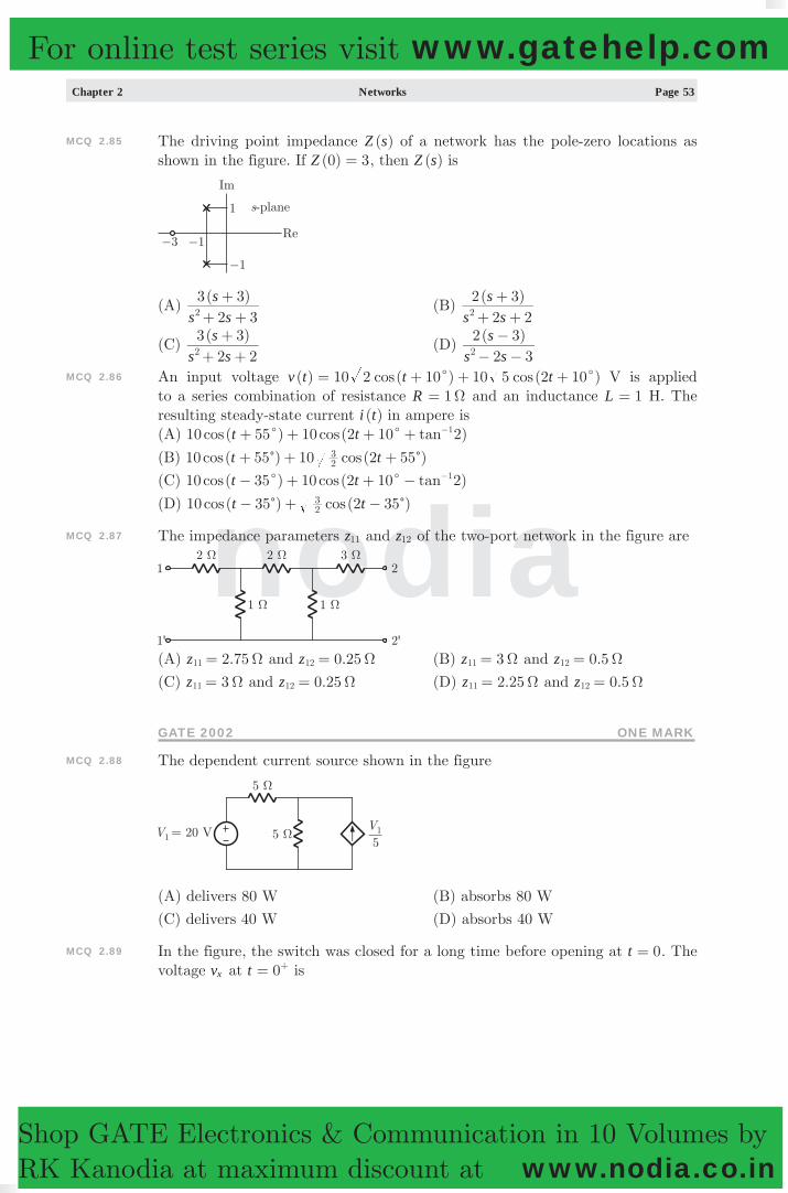
Chapter 2 Networks Page 53
nodia
Shop GATE Electronics & Communication in 10 Volumes by RK Kanodia at maximum discount at www.nodia.co.in
For online test series visit www.gatehelp.com
MCQ 2.85 The driving point impedance ( )Z s of a network has the pole-zero locations as shown in the figure. If ( )Z 0 3= , then ( )Z s is
(A) ( )
s ss2 3
3 32 + +
+ (B)
( )s s
s2 2
2 32 + +
+
(C) ( )
s ss2 2
3 32 + +
+ (D)
( )s s
s2 3
2 32 - -
-
MCQ 2.86 An input voltage ( ) 10 ( 10 ) 10 ( )cos cosv t t t2 5 2 10c c= + + + V is applied to a series combination of resistance R 1W= and an inductance L 1= H. The resulting steady-state current ( )i t in ampere is(A) 10 ( 55 ) 10 (2 10 2)cos cos tant t 1c c+ + + + -
(B) 10 ( 55 ) 10 (2 55 )cos cost t23c c+ + +
(C) 10 ( 35 ) 10 (2 10 2)cos cos tant t 1c c- + + - -
(D) 10 ( 35 ) (2 35 )cos cost t23c c- + -
MCQ 2.87 The impedance parameters z11 and z12 of the two-port network in the figure are
(A) . 5z 2 711 W= and 0. 5z 212 W= (B) 3z11 W= and .z 0 512 W=(C) z 311 W= and 0. 5z 212 W= (D) 2.25z11 W= and 0.5z12 W=
GATE 2002 ONE MARK
MCQ 2.88 The dependent current source shown in the figure
(A) delivers 80 W (B) absorbs 80 W
(C) delivers 40 W (D) absorbs 40 W
MCQ 2.89 In the figure, the switch was closed for a long time before opening at t 0= . The voltage vx at t 0= + is

Page 54 Networks Chapter 2
nodia
Shop GATE Electronics & Communication in 10 Volumes by RK Kanodia at maximum discount at www.nodia.co.in
For online test series visit www.gatehelp.com
(A) 25 V (B) 50 V
(C) 05- V (D) 0 V
GATE 2002 TWO MARKS
MCQ 2.90 In the network of the fig, the maximum power is delivered to RL if its value is
(A) 16 W (B) 340 W
(C) 60 W (D) 20 W
MCQ 2.91 If the 3-phase balanced source in the figure delivers 1500 W at a leading power factor 0.844 then the value of ZL (in ohm) is approximately
(A) .90 32 44c+ (B) .80 32 44c+
(C) .80 32 44c+- (D) .90 32 44c+-
GATE 2001 ONE MARK
MCQ 2.92 The Voltage e0 in the figure is
(A) 2 V (B) /4 3 V
(C) 4 V (D) 8 V
MCQ 2.93 If each branch of Delta circuit has impedance Z3 , then each branch of the equivalent Wye circuit has impedance
(A) Z3
(B) Z3

Chapter 2 Networks Page 55
nodia
Shop GATE Electronics & Communication in 10 Volumes by RK Kanodia at maximum discount at www.nodia.co.in
For online test series visit www.gatehelp.com
(C) 3 Z3 (D) Z3
MCQ 2.94 The admittance parameter Y12 in the 2-port network in Figure is
(A) .0 02- mho (B) 0.1 mho
(C) 0.05- mho (D) 0.05 mho
GATE 2001 TWO MARKS
MCQ 2.95 The voltage e0 in the figure is
(A) 48 V (B) 24 V
(C) 36 V (D) 28 V
MCQ 2.96 When the angular frequency w in the figure is varied 0 to 3, the locus of the current phasor I2 is given by
MCQ 2.97 In the figure, the value of the load resistor RL which maximizes the power delivered

Page 56 Networks Chapter 2
nodia
Shop GATE Electronics & Communication in 10 Volumes by RK Kanodia at maximum discount at www.nodia.co.in
For online test series visit www.gatehelp.com
to it is
(A) .14 14 W (B) 10 W(C) 200 W (D) .28 28W
MCQ 2.98 The z parameters z11 and z21 for the 2-port network in the figure are
(A) ;z z116
1116
11 21W W= = (B) ;z z116
114
11 21W W= =
(C) ;z z116
1116
11 21W W= =- (D) ;z z114
114
11 21W W= =
GATE 2000 ONE MARK
MCQ 2.99 The circuit of the figure represents a
(A) Low pass filter (B) High pass filter
(C) band pass filter (D) band reject filter
MCQ 2.100 In the circuit of the figure, the voltage ( )v t is
(A) e eat bt- (B) e eat bt+(C) ae beat bt- (D) ae beat bt+
MCQ 2.101 In the circuit of the figure, the value of the voltage source E is

Chapter 2 Networks Page 57
nodia
Shop GATE Electronics & Communication in 10 Volumes by RK Kanodia at maximum discount at www.nodia.co.in
For online test series visit www.gatehelp.com
(A) 16- V (B) 4 V
(C) 6- V (D) 16 V
GATE 2000 TWO MARKS
MCQ 2.102 Use the data of the figure (a). The current i in the circuit of the figure (b)
(A) 2- A (B) 2 A
(C) 4- A (D) 4 A
GATE 1999 ONE MARK
MCQ 2.103 Identify which of the following is NOT a tree of the graph shown in the given figure is
(A) begh (B) defg
(C) abfg (D) aegh
MCQ 2.104 A 2-port network is shown in the given figure. The parameter h21 for this network can be given by
(A) /1 2- (B) /1 2+

Page 58 Networks Chapter 2
nodia
Shop GATE Electronics & Communication in 10 Volumes by RK Kanodia at maximum discount at www.nodia.co.in
For online test series visit www.gatehelp.com
(C) /3 2- (D) /3 2+
GATE 1999 TWO MARK
MCQ 2.105 The Thevenin equivalent voltage VTH appearing between the terminals A and B of the network shown in the given figure is given by
(A) ( )j j16 3 4- (B) ( )j j16 3 4+(C) ( )j16 3 4+ (D) ( )j16 3 4-
MCQ 2.106 The value of R (in ohms) required for maximum power transfer in the network shown in the given figure is
(A) 2 (B) 4
(C) 8 (D) 16
MCQ 2.107 A Delta-connected network with its Wye-equivalent is shown in the given figure. The resistance ,R R1 2 and R3 (in ohms) are respectively
(A) 1.5, 3 and 9 (B) 3, 9 and 1.5
(C) 9, 3 and 1.5 (D) 3, 1.5 and 9
GATE 1998 ONE MARK
MCQ 2.108 A network has 7 nodes and 5 independent loops. The number of branches in the network is(A) 13 (B) 12
(C) 11 (D) 10
MCQ 2.109 The nodal method of circuit analysis is based on(A) KVL and Ohm’s law (B) KCL and Ohm’s law
(C) KCL and KVL (D) KCL, KVL and Ohm’s law
MCQ 2.110 Superposition theorem is NOT applicable to networks containing
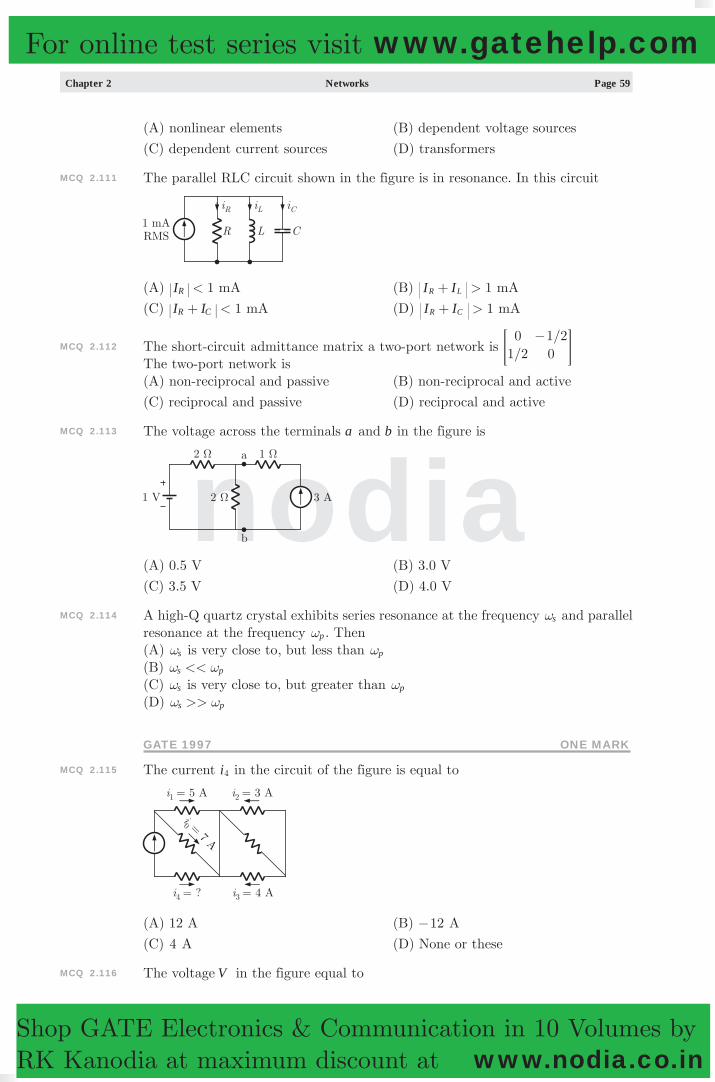
Chapter 2 Networks Page 59
nodia
Shop GATE Electronics & Communication in 10 Volumes by RK Kanodia at maximum discount at www.nodia.co.in
For online test series visit www.gatehelp.com
(A) nonlinear elements (B) dependent voltage sources
(C) dependent current sources (D) transformers
MCQ 2.111 The parallel RLC circuit shown in the figure is in resonance. In this circuit
(A) I 1<R mA (B) I I 1>R L+ mA
(C) I I 1<R C+ mA (D) I I 1>R C+ mA
MCQ 2.112 The short-circuit admittance matrix a two-port network is //0
1 21 20
-> H
The two-port network is(A) non-reciprocal and passive (B) non-reciprocal and active
(C) reciprocal and passive (D) reciprocal and active
MCQ 2.113 The voltage across the terminals a and b in the figure is
(A) 0.5 V (B) 3.0 V
(C) 3.5 V (D) 4.0 V
MCQ 2.114 A high-Q quartz crystal exhibits series resonance at the frequency sw and parallel resonance at the frequency pw . Then(A) sw is very close to, but less than pw(B) <<s pw w(C) sw is very close to, but greater than pw(D) >>s pw w
GATE 1997 ONE MARK
MCQ 2.115 The current i4 in the circuit of the figure is equal to
(A) 12 A (B) 12- A
(C) 4 A (D) None or these
MCQ 2.116 The voltage V in the figure equal to

Page 60 Networks Chapter 2
nodia
Shop GATE Electronics & Communication in 10 Volumes by RK Kanodia at maximum discount at www.nodia.co.in
For online test series visit www.gatehelp.com
(A) 3 V (B) 3- V
(C) 5 V (D) None of these
MCQ 2.117 The voltage V in the figure is always equal to
(A) 9 V (B) 5 V
(C) 1 V (D) None of the above
MCQ 2.118 The voltage V in the figure is
(A) 10 V (B) 15 V
(C) 5 V (D) None of the above
MCQ 2.119 In the circuit of the figure is the energy absorbed by the 4 W resistor in the time interval ( , )0 3 is
(A) 36 Joules (B) 16 Joules
(C) 256 Joules (D) None of the above
MCQ 2.120 In the circuit of the figure the equivalent impedance seen across terminals , ,a b is

Chapter 2 Networks Page 61
nodia
Shop GATE Electronics & Communication in 10 Volumes by RK Kanodia at maximum discount at www.nodia.co.in
For online test series visit www.gatehelp.com
(A) 316 Wb l (B) 3
8 Wb l
(C) j38 12 W+b l (D) None of the above
GATE 1996 ONE MARK
MCQ 2.121 In the given figure, ,A A1 2 and A3 are ideal ammeters. If A2 and A3 read 3 A and 4 A respectively, then A1 should read
(A) 1 A (B) 5 A
(C) 7 A (D) None of these
MCQ 2.122 The number of independent loops for a network with n nodes and b branches is(A) n 1-(B) b n-(C) b n 1- +(D) independent of the number of nodes
GATE 1996 TWO MARKS
MCQ 2.123 The voltages , ,V VC C1 2 and VC3 across the capacitors in the circuit in the given figure, under steady state, are respectively.
(A) 80 V, 32 V, 48 V (B) 80 V, 48 V, 32 V
(C) 20 V, 8 V, 12 V (D) 20 V, 12 V, 8 V

Page 62 Networks Chapter 2
nodia
Shop GATE Electronics & Communication in 10 Volumes by RK Kanodia at maximum discount at www.nodia.co.in
For online test series visit www.gatehelp.com
***********

Chapter 2 Networks Page 63
nodia
Shop GATE Electronics & Communication in 10 Volumes by RK Kanodia at maximum discount at www.nodia.co.in
For online test series visit www.gatehelp.com
SOLUTIONS
SOL 2.1 Option (B) is correct.In the equivalent star connection, the resistance can be given as
RC R R RR R
a b c
b a= + +
RB R R RR R
a b c
a c= + +
RA R R RR R
a b c
b c= + +
So, if the delta connection components Ra , Rb and Rc are scaled by a factor k
then
RAl kR kR kRk R k Ra b c
b c= + +^ ^h h
kk
R R RR R
a b c
b c2
= + + k RA=
Hence, it is also scaled by a factor k
SOL 2.2 Option (D) is correct.For the given capacitance, C F100m= in the circuit, we have the reactance.
XC sc1=
s 100 101
6# #
= - s104
=
So,
V sV s
1
2
^
^
h
h
10 10
s s
s10 10 10
44
44
4=+ +
+ s
s21= +
+
SOL 2.3 Option (C) is correct.For the purely resistive load, maximum average power is transferred when RL R XTh Th
2 2= +where R jXTh Th+ is the equivalent thevenin (input) impedance of the circuit. Hence, we obtain RL 4 32 2= + 5W
SOL 2.4 Option (C) is correct.For evaluating the equivalent thevenin voltage seen by the load RL , we open the circuit across it (also if it consist dependent source).The equivalent circuit is shown below
As the circuit open across RL so
I2 0=or, 40j I2 0=

Page 64 Networks Chapter 2
nodia
Shop GATE Electronics & Communication in 10 Volumes by RK Kanodia at maximum discount at www.nodia.co.in
For online test series visit www.gatehelp.com
i.e., the dependent source in loop 1 is short circuited. Therefore,
VL1 jj V4 34 s= +
^ h
VTh V10 L1= 100 53.13jj4 340
c= + .
100 53.135 53 1340 90
cc
c=
800 90c=
SOL 2.5 Option (C) is correct.For the given transformer, we have
VVWX
.1
1 25=
Since, VVYZ .0 8= (attenuation factor)
So, VV
WX
YZ . .0 8 1 25 1= =^ ^h h
or, VYZ VWX=
at VWX1 100 V= ; VV
100100
WX
YZ
1
1 =
at VWZ2 100 V= ; VV
100100
YZ
WX
2
2 =
SOL 2.6 Option (C) is correct.The quality factor of the inductances are given by
q1 RL1
1w=
and q2 RL2
2w=
So, in series circuit, the effective quality factor is given by
Q RX
R RL L
eq
Leq
1 2
1 2w w= = ++
R R
R RL
R RL
1 12 1
1 2
1
1 2
2w w=
+
+
R R
Rq
Rq
1 12
1
2
2
2 1
=+
+ R R
q R q R1 2
1 1 2 2= ++
SOL 2.7 Option (C) is correct.
Consider that the voltage across the three capacitors C1, C2 and C3 are V1, V2 and V3 respectively. So, we can write
VV
3
2 CC
2
3= ....(1)
Since, Voltage is inversely proportional to capacitance

Chapter 2 Networks Page 65
nodia
Shop GATE Electronics & Communication in 10 Volumes by RK Kanodia at maximum discount at www.nodia.co.in
For online test series visit www.gatehelp.com
Now, given that C1 F10 m= ; 10VV max1 =^ h
C2 F5 m= ; 5 VV max2 =^ h
C3 F2 m= ; 2VV max3 =^ h
So, from Eq (1) we have
VV
3
2 52=
for V max3^ h 2=
We obtain, V2 0.8 volt52 2 5<#= =
i.e., V2 V< max2^ hHence, this is the voltage at C2. Therefore, V3 2 volt= V2 0.8 volt=and V1 2.8 voltV V2 3= + =Now, equivalent capacitance across the terminal is
Ceq C CC C C2 3
2 31= + + 5 2
5 2 10#= + + F780 m=
Equivalent voltage is (max. value) Vmax .V 2 81= =So, charge stored in the effective capacitance is
Q C Vmaxeq= .780 2 8#= b ^l h 32 Cm=
SOL 2.8 Option (D) is correct.
At the node 1, voltage is given as V1 10 volt=Applying KCL at node 1
I V V2 1 2 0S1 1+ + - =
2I 210
110 0S + + - =
13 AIS =-Also, from the circuit, V 5 2S #- V1= & VS V10 1= + 20 volt=
SOL 2.9 Option (C) is correct.Again from the shown circuit, the current in 1W resistor is
I 10 AV1 1
101= = =
SOL 2.10 Option (D) is correct.The s -domain equivalent circuit is shown as below.

Page 66 Networks Chapter 2
nodia
Shop GATE Electronics & Communication in 10 Volumes by RK Kanodia at maximum discount at www.nodia.co.in
For online test series visit www.gatehelp.com
( )I s ( )/ ( )
C s C s
v s
C C
v1 1
01 1
0c c
1 2 1 2
=+
=+
( )I s (12 )VC CC C1 2
1 2= +b l 12Ceq= (0) 12 VvC =
Taking inverse Laplace transform for the current in time domain,
( )i t ( )C t12 eqd= (Impulse)
SOL 2.11 Option (B) is correct.
In phasor form, Z j4 3= - 5 .36 86cW= - I 5 A100c=Average power delivered.
P .avg cosZI21 2 q= 25 5 36.86cos2
1# c#= 50 W=
Alternate Method: Z (4 3)j W= - , I 5 (100 100)cos Atp= +
Pavg Re I Z21 2= $ . ( ) ( )Re j2
1 5 4 32# #= -" , 100 50 W2
1#= =
SOL 2.12 Option (C) is correct
Applying nodal analysis at top node.
1 1j
V V1
01
01 1c c+ + + 1 0c=
( 1 1) 1 1j jV 01 c+ + + j1=
V1 j1 11= +
-
Current I1 1
j jjV
10
11
1 11 c= + =
- + +
( )A
j jj
j1 11= + = +

Chapter 2 Networks Page 67
nodia
Shop GATE Electronics & Communication in 10 Volumes by RK Kanodia at maximum discount at www.nodia.co.in
For online test series visit www.gatehelp.com
SOL 2.13 Option (A) is correct.We obtain Thevenin equivalent of circuit B .
Thevenin Impedance :
ZTh R=
Thevenin Voltage : VTh 3 V0c=Now, circuit becomes as
Current in the circuit, I1 R210 3= +
-
Power transfer from circuit toA B
P ( ) 3I R I12 2
1= +
10 3 10 3R R R2 3 2
2= +
- + +-
: :D D
or P ( )42 70
RR
2 2=++
dRdP
( )( ) ( ) ( )
RR R R
22 70 42 70 2 2
04
2
=+
+ - + + =
(2 )[(2 )70 (42 70 )2]R R R+ + - + 0= & R 0.8W=
SOL 2.14 Option (A) is correct.
In the given circuit
V VA B- 6 V=So current in the branch will be
IAB 3 A26= =
We can see, that the circuit is a one port circuit looking from terminal BD as shown below

Page 68 Networks Chapter 2
nodia
Shop GATE Electronics & Communication in 10 Volumes by RK Kanodia at maximum discount at www.nodia.co.in
For online test series visit www.gatehelp.com
For a one port network current entering one terminal, equals the current leaving the second terminal. Thus the outgoing current from A to B will be equal to the incoming current from D to C as shown
i.e. IDC 3 AIAB= =
The total current in the resistor 1W will be
I1 2 IDC= + (By writing KCL at node D)
2 3 5 A= + =So, VCD ( )I1 1#= - 5 V=-
SOL 2.15 Option (C) is correct.When 10 V is connected at port A the network is
Now, we obtain Thevenin equivalent for the circuit seen at load terminal, let Thevenin voltage is V , VTh 10 with 10 V applied at port A and Thevenin resistance is RTh .
IL R RV ,10 V
Th L
Th= +For 1RL W= , 3 AIL =
3 RV
1,10 V
Th
Th= + ...(i)

Chapter 2 Networks Page 69
nodia
Shop GATE Electronics & Communication in 10 Volumes by RK Kanodia at maximum discount at www.nodia.co.in
For online test series visit www.gatehelp.com
For 2.5RL W= , 2 AIL =
2 .RV
2 5,10 V
Th
Th= + ...(ii)
Dividing above two
23 .
RR
12 5
Th
Th= ++
R3 3Th + R2 5Th= + RTh 2W=Substituting RTh into equation (i)
V ,10 VTh 3(2 1) 9 V= + =Note that it is a non reciprocal two port network. Thevenin voltage seen at port B depends on the voltage connected at port A. Therefore we took subscript V ,10 VTh . This is Thevenin voltage only when 10 V source is connected at input port
.A If the voltage connected to port A is different, then Thevenin voltage will be different. However, Thevenin’s resistance remains same.Now, the circuit is as shown below :
For 7RL W= , IL 1 ARV2 2 7
9,10 V
L
Th= + = + =
SOL 2.16 Option (B) is correct.Now, when 6 V connected at port A let Thevenin voltage seen at port B is V ,6 VTh
. Here 1RL W= and AI 37
L =
V , VTh 6 R 37 1 3
7Th # #= + 2 7 V3
737
#= + =
This is a linear network, so VTh at port B can be written as
VTh V1a b= +where V1 is the input applied at port A.We have 10 VV1 = , 9 VV ,10 VTh =
9 10a b= + ...(i)When 6 VV1 = , 9 VV , VTh 6 =
7 6a b= + ...(ii)Solving (i) and (ii)
a .0 5= , 4b =Thus, with any voltage V1 applied at port A, Thevenin voltage or open circuit voltage at port B will be

Page 70 Networks Chapter 2
nodia
Shop GATE Electronics & Communication in 10 Volumes by RK Kanodia at maximum discount at www.nodia.co.in
For online test series visit www.gatehelp.com
So, V ,Th V1 . V0 5 41= +For V1 8 V= V ,8 VTh . V0 5 8 4 8 oc#= + = = (open circuit voltage)
SOL 2.17 Option (A) is correct.Replacing P Q- by short circuit as shown below we have
Using current divider rule the current Isc is
ISC 25 (16 )j25 15 30 0= + + (6.4 4.8)Aj= -
SOL 2.18 Option (C) is correct.Power transferred to RL will be maximum when RL is equal to the Thevenin resistance. We determine Thevenin resistance by killing all source as follows :
RTH 10 1010 10 10#= + + 15W=
SOL 2.19 Option (A) is correct.The given circuit is shown below
For parallel combination of R and C equivalent impedance is
Zp R j C
R j Cj RCR
1
1
1
$
w
ww=
+= +
Transfer function can be written as
VV
in
out Z ZZ
s p
p= + R j C j RC
Rj RCR
11
1
w w
w=+ + +
+
( )j RC j RC
j RC1 2w w
w=+ +
( )j j
j1 2=
+ + Here RC
1w =

Chapter 2 Networks Page 71
nodia
Shop GATE Electronics & Communication in 10 Volumes by RK Kanodia at maximum discount at www.nodia.co.in
For online test series visit www.gatehelp.com
VV
in
out ( )j j
j1 3
12=
+ +=
Thus vout ( / )cosV
t RC3p= b l
SOL 2.20 Option (B) is correct.
From star delta conversion we have
Thus R1 . 2R R R
R R6 6 6
6 6a b c
a b W= + + = + + =
Here R1 R R 22 3 W= = =Replacing in circuit we have the circuit shown below :
Now the total impedance of circuit is
Z (2 4)(2 4)(2 4)(2 4)
j jj j
2 7 W= + -+ - + =
Current I 2 0714 0c c+ += =
SOL 2.21 Option (D) is correct.
From given admittance matrix we get
I1 0.1 0.01V V1 2= - and ...(1)
I2 0.01 0.1V V1 2= + ...(2)
Now, applying KVL in outer loop;
V2 I100 2=-or I2 . V0 01 2=- ...(3)
From eq (2) and eq (3) we have
. V0 01 2- . .V V0 01 0 11 2= + . V0 11 2- . V0 01 1=
VV
1
2 111= -
SOL 2.22 Option (A) is correct.Here we take the current flow direction as positive.At t 0= - voltage across capacitor is

Page 72 Networks Chapter 2
nodia
Shop GATE Electronics & Communication in 10 Volumes by RK Kanodia at maximum discount at www.nodia.co.in
For online test series visit www.gatehelp.com
( )V 0C- C
Q=- . 50 V50 102 5 10
6
3
##=- =--
-
Thus (0 )VC+ 50 V=-
In steady state capacitor behave as open circuit thus
( )V 3 100 V=Now, ( )V tC ( ) ( (0 ) ( ))V V V e /
C C Ct RC3 3= + -+ -
t
10 50 10 6# #
--
( )e100 50 100= + - -
e100 150 ( )t2 103
= - #-
Now ( )i tc C dtdV=
50 10 150 2 10 Ae t6 3 2 103
# # # #= #- -
15e t2 103
= #-
( )i tc 15 ( 2 10 )exp At3#= -
SOL 2.23 Option (A) is correct.Given circuit is as shown below
Writing node equation at input port
I1 . .V V V0 5 0 5
1 1 2= + - V V4 21 2= - ...(1)
Writing node equation at output port
I2 . .V V V0 5 0 5
2 2 1= + - V V2 41 2=- + ...(2)
From (1) and (2), we have admittance matrix
Y 42
24= -
-> H
SOL 2.24 Option (D) is correct.A parallel RLC circuit is shown below :
Input impedance Zin
R j L j C1 11
w w=
+ +
At resonance L1w Cw=
So, Zin /RR
11= = (maximum at resonance)
Thus (D) is not true.

Chapter 2 Networks Page 73
nodia
Shop GATE Electronics & Communication in 10 Volumes by RK Kanodia at maximum discount at www.nodia.co.in
For online test series visit www.gatehelp.com
Furthermore bandwidth is Bw i.e R1
B \w and is independent of L ,
Hence statements A, B, C, are true.
SOL 2.25 Option (A) is correct.
Let the current ( )i t A Be /t= + t- "t Time constantWhen the switch S is open for a long time before t 0< , the circuit is
At t 0= , inductor current does not change simultaneously, So the circuit is
Current is resistor (AB)
( )i 0 . 0.375 A20 75= =
Similarly for steady state the circuit is as shown below
( )i 3 0.5 A315= =
t RL
eq=
( || )sec
10 10 1015 10 10
33#= + =
--
( )i t A Bet
1 10 3= + #- - A Be t100= + -
Now ( )i 0 .A B 0 375= + =and ( )i 3 .A 0 5= =So, B . .0 375 0 5= - .0 125=-Hence ( )i t 0. 0.125 Ae5 t1000= - -
SOL 2.26 Option (A) is correct.Circuit is redrawn as shown below
Where, Z1 j L j j10 20 10 203 3# # #w= = =-
Z2 ||R XC=
XC j C jj1
10 50 101 203 6
# # #w= = =--

Page 74 Networks Chapter 2
nodia
Shop GATE Electronics & Communication in 10 Volumes by RK Kanodia at maximum discount at www.nodia.co.in
For online test series visit www.gatehelp.com
Z2 ( )
jj
1 201 20= -
- 1R W=
Voltage across Z2
VZ2 20Z ZZ 0
1 2
2 := + 20j j
jj
j
20 1 2020
1 2020
:=- -
--
c
c
m
m
( 20 )
20j jj
j20 400 20 := + -- =-c m
Current in resistor R is
I RVZ2= Aj j1=- =-
SOL 2.27 Option (A) is correct.The circuit can be redrawn as
Applying nodal analysis
V V2
10 1 20A A- + + - 0=
V2 10 2A - + 0 4 VV4= = =
Current, I1 3 A210 4= - =
Current from voltage source is
I2 I 3 01= - =Since current through voltage source is zero, therefore power delivered is zero.
SOL 2.28 Option (A) is correct.Circuit is as shown below
Since 60 V source is absorbing power. So, in 60 V source current flows from + to - ve direction
So, I I1+ 12= I I12 1= -

Chapter 2 Networks Page 75
nodia
Shop GATE Electronics & Communication in 10 Volumes by RK Kanodia at maximum discount at www.nodia.co.in
For online test series visit www.gatehelp.com
I is always less then 12 A So, only option (A) satisfies this conditions.
SOL 2.29 Option (C) is correct.For given network we have
V0 ( )( )
R R XR X V
L C
L C i=+
( )( )
V sV s
i
0 R
sR CR
sR CR
1
1
L
L
L
L
=+
+
+ R RR sC R
RL L
L=+ +
R RR sC R
RL L
L=+ +
RR RsC1
1
L
=+ +
But we have been given
. .T F ( )( )
V sV s
i
0= sCR21=
+Comparing, we get
RR1
L+ 2= & RL R=
SOL 2.30 Option (C) is correct.The energy delivered in 10 minutes is
E VIdt I Vdttt
00= = ## I Area#=
( ) .221 10 12 600 13 2# #= + = kJ
SOL 2.31 Option (B) is correct.From given circuit the load current is
IL Z Z
Vs L
=+
( ) ( )j j j1 2 7 4
20 08 620 0c c+ +=
+ + +=
+
( )j51 8 6= -
1020 0c
++f
= 2+ f= - where tan431f = -
The voltage across load is
VL I ZL L=The reactive power consumed by load is
Pr V I*L L= I Z I Z I*
L L L L L2#= =
(7 4 )j j8 620 0 2c+
#= + ( )j j7 4 28 16= + = +
Thus average power is 28 and reactive power is 16.
SOL 2.32 Option (B) is correct.At 0t = -, the circuit is as shown in fig below :
(0 ) 100V =- VThus (0 ) 100V =+ VAt t 0= +, the circuit is as shown below

Page 76 Networks Chapter 2
nodia
Shop GATE Electronics & Communication in 10 Volumes by RK Kanodia at maximum discount at www.nodia.co.in
For online test series visit www.gatehelp.com
( )Ik
05100 20= =+ mA
At steady state i.e. at t 3= is ( )I 3 0=
Now ( )i t (0 ) ( )I e u tRCt
eq= + -
Ceq . . .( . . ) .
0.160 5 0 3 0 20 5 0 3 0 2m m mm m m m=+ ++ = F
RC
1eq
.
12505 10 0 16 10
13 6
# # #= =-
( )i t 20 ( )e u tt1250= - mA
SOL 2.33 Option (C) is correct.For Pmax the load resistance RL must be equal to thevenin resistance Req i.e. RL
Req= . The open circuit and short circuit is as shown below
The open circuit voltage is
Voc 100= V
From fig I1 .8
100 12 5= = A
Vx .4 12 5 50#=- =- V
I2 .V4
1004
100 50 12 5x= + = - = A
Isc I I 251 2= + = A
Rth 4IV
25100
sc
oc W= = =
Thus for maximum power transfer RL 4Req W= =
SOL 2.34 Option (A) is correct.Steady state all transient effect die out and inductor act as short circuits and forced response acts only. It doesn’t depend on initial current state. From the given time domain behavior we get that circuit has only R and L in series with V0. Thus at steady state
( ) ( )i t i" 3 RV0=
SOL 2.35 Option (C) is correct.The given graph is

Chapter 2 Networks Page 77
nodia
Shop GATE Electronics & Communication in 10 Volumes by RK Kanodia at maximum discount at www.nodia.co.in
For online test series visit www.gatehelp.com
There can be four possible tree of this graph which are as follows:
There can be 6 different possible cut-set.
SOL 2.36 Option (B) is correct.Initially (0 ) 0i =- therefore due to inductor (0 ) 0i =+ . Thus all current Is will flow in resistor R and voltage across resistor will be I Rs s . The voltage across inductor will be equal to voltage across Rs as no current flow through R.
Thus ( )v 0L+ I Rs s=
but ( )v 0L+
( )L dt
di 0=+
Thus ( )dt
di 0+
( )L
vL
I R0L s s= =+
SOL 2.37 Option (A) is correct.Killing all current source and voltage sources we have,
Zth ( ) ( )s1 1s1= + +
( ) ( )( )( ) [ ]
ss
ss
1 11 1
1 11 1
s
s
s
s1
1
1
1
=+ + ++ + =
+ + ++ + +
or Zth 1=Alternative :Here at DC source capacitor act as open circuit and inductor act as short
circuit. Thus we can directly calculate thevenin Impedance as 1 W

Page 78 Networks Chapter 2
nodia
Shop GATE Electronics & Communication in 10 Volumes by RK Kanodia at maximum discount at www.nodia.co.in
For online test series visit www.gatehelp.com
SOL 2.38 Option (D) is correct.
( )Z s RsC
sLs
1
RCs
LC
Cs
2 1= =
+ +We have been given
( )Z s ..
s ss
0 1 20 2
2=+ +
Comparing with given we get
C1 .0 2= or C 5= F
RC1 .0 1= or 2R W=
LC1 2= or .L 0 1= H
SOL 2.39 Option (C) is correct.Voltage across capacitor is
Vc Cidt1 t
0= #
Here C 1= F and i 1= A. Therefore
Vc dtt
0= #
For t T0 < < , capacitor will be charged from 0 V
Vc dt tt
0= =#
At ,t T V Tc= = Volts
For T t T2< < , capacitor will be discharged from T volts as
Vc T dt T t2T
t= - = -#
At 2 , 0t T Vc= = volts
For T t T2 3< < , capacitor will be charged from 0 V
Vc dt t T2T
t
2= = -#
At 3 ,t T V Tc= = Volts
For T t T3 4< < , capacitor will be discharged from T Volts
Vc T dt T t4T
t
3= - = -#
At 4 , 0t T Vc= = Volts
For T t T4 5< < , capacitor will be charged from 0 V
Vc dt t T4T
t
4= = -#
At 5 ,t T V Tc= = Volts
Thus the output waveform is

Chapter 2 Networks Page 79
nodia
Shop GATE Electronics & Communication in 10 Volumes by RK Kanodia at maximum discount at www.nodia.co.in
For online test series visit www.gatehelp.com
Only option C satisfy this waveform.
SOL 2.40 Option (D) is correct.Writing in transform domain we have
( )( )
V sV s
s
c s 1s
s1
1=
+ +^ h
( )s s 11
2=+ +
Since ( ) ( ) ( )V t t V s 1s s"d= = and
( )V sc ( )s s 1
12=+ +
or ( )V sc ( )s3
2
21 2
43
23
=+ += G
Taking inverse Laplace transform we have
Vt sine t3
223t
2= -c m
SOL 2.41 Option (B) is correct.Let voltage across resistor be vR
( )( )
V sV s
S
R ( ) ( )s s s
s1
11s
1 2=+ +
=+ +
Since ( ) ( )v t V s 1s s"d= = we get
( )V sR ( ) ( )s s
ss
s12
21 2
43
=+ +
=+ +
( )
( )( )s
ss2
1 243
21
21 2
43
21
=+ +
+-
+ +
or ( )v tR cos sine t e t23
21
32
23
21
21
#= -- -
cos sine t t23
31
23t
2= --= G
SOL 2.42 Option (C) is correct.From the problem statement we have
z11 .iv
46 1 5
i1
1
02
W= = ==
z12 . .iv
14 5 4 5
i2
1
01
W= = ==
z21 .iv
46 1 5
i1
2
02
W= = ==
z22 . .iv
11 5 1 5
i2
2
02
W= = ==
Thus z -parameter matrix is
zz
zz
11
21
12
22= G
.
...
1 51 5
4 51 5= = G
SOL 2.43 Option (A) is correct.From the problem statement we have
h12 ..
vv
1 54 5 3
i2
1
01
= = ==
h22 ..
vi
1 51 0 67
i2
2
01
= = ==
From z matrix, we have

Page 80 Networks Chapter 2
nodia
Shop GATE Electronics & Communication in 10 Volumes by RK Kanodia at maximum discount at www.nodia.co.in
For online test series visit www.gatehelp.com
v1 z i z i11 1 12 2= + v2 z i z i21 1 22 2= +
If v 02 = then ii1
2 ..
zz h
1 51 5 1
22
2121= - = - =- =
or i2 i1=-Putting in equation for v1, we get
v1 ( )z z i11 12 1= -
iv
v1
1
02 = h z z11 11 12= = - . .1 5 4 5 3= - =-
Hence h -parameter will be
hh
hh
11
21
12
22= G .
31
30 67=
--= G
SOL 2.44 Option (D) is correct.According to maximum Power Transform Theorem
ZL ( )Z R jX*s s s= = -
SOL 2.45 Option (C) is correct.At " 3w , capacitor acts as short circuited and circuit acts as shown in fig below
Here we get VV 0
i
0 =
At 0"w , capacitor acts as open circuited and circuit look like as shown in fig below
Here we get also VV 0
i
0 =
So frequency response of the circuit is as shown in fig and circuit is a Band pass filter.
SOL 2.46 Option (D) is correct.
We know that bandwidth of series RLC circuit is LR . Therefore
Bandwidth of filter 1 is BLR
11
=
Bandwidth of filter 2 is /
BLR
LR
LR
44
22 1 1
= = =
Dividing above equation BB
41
2
1 =

Chapter 2 Networks Page 81
nodia
Shop GATE Electronics & Communication in 10 Volumes by RK Kanodia at maximum discount at www.nodia.co.in
For online test series visit www.gatehelp.com
SOL 2.47 Option (D) is correct.Here Vth is voltage across node also. Applying nodal analysis we get
V V V i2 1 1
2th th th+ + - 2=
But from circuit i V V1th
th= =
Therefore
V V V V2 1 1
2th th th th+ + - 2=
or Vth 4= volt
From the figure shown below it may be easily seen that the short circuit current
at terminal XY is i 2sc = A because i 0= due to short circuit of 1 W resistor
and all current will pass through short circuit.
Therefore Rth 2iV
24
sc
th W= = =
SOL 2.48 Option (A) is correct.The voltage across capacitor isAt t 0= +, ( )V 0 0c =+
At t 3= , ( )V 5C 3 = V
The equivalent resistance seen by capacitor as shown in fig is
Req k20 20 10 W= =
Time constant of the circuit is
t .R C k10 4 0 04eq # m= = = s
Using direct formula
( )V tc ( ) [ ( ) (0)]V V V e /C c c
t3 3= - - t-
( )(1 ) (0)V e V e/ /C
tC
t3= - +t t- - 5(1 )e / .t 0 04= - -
or ( )V tc 5(1 )e t25= - -

Page 82 Networks Chapter 2
nodia
Shop GATE Electronics & Communication in 10 Volumes by RK Kanodia at maximum discount at www.nodia.co.in
For online test series visit www.gatehelp.com
Now ( )I tC ( )
Cdt
dV tC=
4 10 ( 5 25 )e t6 25# # #= -- - 0.5e t25= - mA
SOL 2.49 Option (D) is correct.
Impedance (5 3 ) ( )( ) ( )
j jj jj j
5 35 3 5 35 3 5 3#= - + =
- + +- +
( ) ( )j
105 32 2
= - .
1025 9 3 4= + =
VAB = Current # Impedance 5 30 34 17 30#c c+ += =
SOL 2.50 Option (D) is correct.The network is shown in figure below.
Now V1 AV BI2 2= - ...(1)
and I1 CV DI2 2= - ...(2)
also V2 I RL2=- ...(3)
From (1) and (2) we get
Thus IV
1
1 CV DIAV BI
2 2
2 2=--
Substituting value of V2 from (3) we get
Input Impedance Zin C I R DIA I R BI
L
L
2 2
2 2
##=
- -- -
or Zin CR DAR B
L
L=++
SOL 2.51 Option (B) is correct.The circuit is as shown below.
At input port V1 r Ie 1=At output port V2 ( )r I I r I r I0 2 1 0 1 0 2b b= - =- +Comparing standard equation
V1 z I z I11 1 12 2= + V2 z I z I21 1 22 2= + z12 0= and z21 r0b=-
SOL 2.52 Option (B) is correct.For series RC network input impedance is
Zins sCR
sCsRC1 1= + = +

Chapter 2 Networks Page 83
nodia
Shop GATE Electronics & Communication in 10 Volumes by RK Kanodia at maximum discount at www.nodia.co.in
For online test series visit www.gatehelp.com
Thus pole is at origin and zero is at RC1-
For parallel RC network input impedance is
Zin
sCR
sCR
sRCsC
1
1
1=
+=
+
Thus pole is at RC1- and zero is at infinity.
SOL 2.53 Option (A) is correct.
We know v dtLdi=
Taking Laplace transform we get
( )V s ( ) ( )sLI s Li 0= - +
As per given in question
( )Li 0- + 1=- mV
Thus ( )i 0+ 0.521
mHmV= = A
SOL 2.54 Option (B) is correct.At initial all voltage are zero. So output is also zero.
Thus ( )v 00+ 0=
At steady state capacitor act as open circuit.
Thus, ( )v0 3 v54
54 10 8i# #= = =
The equivalent resistance and capacitance can be calculate after killing all
source
Req 0.81 4= = kW Ceq 54 1= = mF
t 0.8 5 4R C k Feq eq mW #= = = ms
( )v t0 ( ) [ ( ) (0 )]v v v e /t0 0 03 3= - - t+ -
8 (8 0)e / .t 0 004= - - -

Page 84 Networks Chapter 2
nodia
Shop GATE Electronics & Communication in 10 Volumes by RK Kanodia at maximum discount at www.nodia.co.in
For online test series visit www.gatehelp.com
( )v t0 8(1 )e / .t 0 004= - - Volts
SOL 2.55 Option (A) is correct.
Here ( )Z s2 ( )R Z sneg 1= +or ( )Z s2 ( ) ( )Re ImR Z s j Z sneg 1 1= + +For ( )Z s2 to be positive real, ( )ReZ s2 0$
Thus ( )ReR Z sneg 1+ 0$
or ( )ReZ s1 Rneg$-But Rneg is negative quantity and Rneg- is positive quantity. Therefore
( )ReZ s1 Rneg$
or Rneg ( )ReZ j1# w For all w.
SOL 2.56 Option (C) is correct.Transfer function is
( )( )
U sY s
R sL
sC
sCs LC scR1
1
11
2=+ +
=+ +
s
LR s
LC
LC1
1
2=
+ +
Comparing with 2 0s sn n2 2xw w+ + = we have
Here 2 nxw LR= ,
and nw LC1=
Thus x L
R LC RLC
2 2= =
For no oscillations, 1$x
Thus RLC
2 1$
or R CL2$
SOL 2.57 Option (B) is correct.For given transformer
II1
2 VV n
12
1= =
or I1 nI2= and V1 nV2=
Comparing with standard equation
V1 AV BI2 2= + I1 CV DI2 2= +
AC
BD= G
n0
0n1= = G
Thus x n1=
SOL 2.58 Option (B) is correct.
We have L H1= and 10C 4001 6
#= -
Resonant frequency
f0 LC2
1p
= = 2 1
4001 10
16# #p
=-

Chapter 2 Networks Page 85
nodia
Shop GATE Electronics & Communication in 10 Volumes by RK Kanodia at maximum discount at www.nodia.co.in
For online test series visit www.gatehelp.com
2
10 20 103 4#p p
= = Hz
SOL 2.59 Option (C) is correct.Maximum power will be transferred when R R 100L s W= =In this case voltage across RL is 5 V, therefore
Pmax .RV
1005 5 0 25
2 #= = = W
SOL 2.60 Option (C) is correct.For stability poles and zero interlace on real axis. In RC series network the driving point impedance is
Zins RCs sC
sRC1 1= + = +
Here pole is at origin and zero is at /s RC1=- , therefore first critical
frequency is a pole and last critical frequency is a zero.
For RC parallel network the driving point impedance is
Zinp R
Cs
RCs
sRCR
1
1
1=
+=
+
Here pole is /s RC1=- and zero is at 3, therefore first critical frequency is a
pole and last critical frequency is a zero.
SOL 2.61 Option (A) is correct.Applying KCL we get
( )i t 5 01 c++ 10 60c+=
or ( )i t1 10 60 5 0c c+ += - j5 5 3 5= + -
or ( )i t1 5 3 90210 3 90c c+ += =
SOL 2.62 Option (B) is correct.If L j51 W= and L j23 W= the mutual induction is subtractive because current enters from dotted terminal of j2W coil and exit from dotted terminal of j5W. If L j22 W= and L j23 W= the mutual induction is additive because current enters from dotted terminal of both coil.
Thus Z L M L M L M M1 13 2 23 3 31 32= - + + + - + j j j j j j j j5 10 2 10 2 10 10 9= + + + + - + =
SOL 2.63 Option (B) is correct.Open circuit at terminal ab is shown below
Applying KCL at node we get
V V5 5
10ab ab+ - 1=
or Vab . V7 5 th= =

Page 86 Networks Chapter 2
nodia
Shop GATE Electronics & Communication in 10 Volumes by RK Kanodia at maximum discount at www.nodia.co.in
For online test series visit www.gatehelp.com
Short circuit at terminal ab is shown below
Short circuit current from terminal ab is
Isc 1510 3= + = A
Thus Rth . 2.5IV
37 5
sc
th W= = =
Here current source being in series with dependent voltage source make it
ineffective.
SOL 2.64 Option (C) is correct.Here V 5a = V because R R1 2= and total voltage drop is 10 V.
Now Vb R RR 10
3 4
3 #=+
.. .
2 11 1 10 5 238#= = V
V V Va b= - .5 5 238= - .0 238=- V
SOL 2.65 Option (D) is correct.For h parameters we have to write V1 and I2 in terms of I1 and V2.
V1 h I h V11 1 12 2= + I2 h I h V21 1 22 2= +Applying KVL at input port
V1 I V10 1 2= +Applying KCL at output port
V20
2 I I1 2= +
or I2 I V201
2=- +
Thus from above equation we get
hh
hh
11
12
12
22= G .
101
10 05= -= G
SOL 2.66 Option (B) is correct.
Time constant RC .0 1 10 10 106 3 4# #= =- - sec
Since time constant RC is very small, so steady state will be reached in 2 sec.
At t 2= sec the circuit is as shown in fig.
Vc 3= V
V2 Vc=- 3=- V

Chapter 2 Networks Page 87
nodia
Shop GATE Electronics & Communication in 10 Volumes by RK Kanodia at maximum discount at www.nodia.co.in
For online test series visit www.gatehelp.com
SOL 2.67 Option (B) is correct.For a tree there must not be any loop. So a, c, and d don’t have any loop. Only b has loop.
SOL 2.68 Option (D) is correct.The sign of M is as per sign of L If current enters or exit the dotted terminals of both coil. The sign of M is opposite of L If current enters in dotted terminal of a coil and exit from the dotted terminal of other coil.
Thus Leq L L M21 2= + -
SOL 2.69 Option (A) is correct.Here 2w = and V 1 0c+=
Y R
j Cj L
1 1ww
= + +
3 2 3 3 4jj
j21
41#
#= + + = +
.tan534 5 53 111 c+ += =-
I * ( )( . ) .V Y 1 0 5 53 1 5 53 1c c c+ + += = =Thus ( )i t ( . )sin t5 2 53 1c= +
SOL 2.70 Option (A) is correct.
( )v ti sin t2 103=
Here w 103= rad and Vi 2 0c+=
Now V0 .R
j C
j C Vj CR
V1
1
11
t i
w
ww
=+
=+
j1 10 10
1 2 03 3# #
c+=+ -
451 c= - ( )v t0 ( )sin t10 453 c= -
SOL 2.71 Option (C) is correct.
Input voltage ( )v ti ( )u t=
Taking Laplace transform ( )V si s1=
Impedance ( )Z s 2s= +
( )I s ( )
( )sV s
s s2 21i=
+=
+
or ( )I s s s2
1 12
1= -+; E
Taking inverse Laplace transform
( )i t (1 ) ( )e u t21 t2= - -
At t 0= , ( )i t 0=At t 2
1= , ( )i t .0 31=At t 3= , ( )i t .0 5=Graph (C) satisfies all these conditions.
SOL 2.72 Option (D) is correct.

Page 88 Networks Chapter 2
nodia
Shop GATE Electronics & Communication in 10 Volumes by RK Kanodia at maximum discount at www.nodia.co.in
For online test series visit www.gatehelp.com
We know that
V1 z I z I11 1 12 2= + V2 z I z I11 1 22 2= +
where z11 IV
I1
1
02
==
z21 IV
I1
2
01
==
Consider the given lattice network, when I 02 = . There is two similar path in
the circuit for the current I1. So I I21
1=
For z11 applying KVL at input port we get
V1 ( )I Z Za b= +
Thus V1 ( )I Z Z21
a b1= +
z11 ( )Z Z21
a b= +
For Z21 applying KVL at output port we get
V2 Z I Z I2 2a b1 1= -
Thus V2 ( )I Z Z21
a b1= -
z21 ( )Z Z21
a b= -
For this circuit z z11 22= and z z12 21= . Thus
zz
zz
11
21
12
22= G
Z Z
Z Z
Z Z
Z Z2
2
2
2
a b
a b
a b
a b=
+
-
-
+
R
T
SSSSS
V
X
WWWWW
Here Z j2a = and Z 2b W=
Thus zz
zz
11
21
12
22= G
jj
jj
11
11=
+-
-+= G
SOL 2.73 Option (B) is correct.Applying KVL,
( )v t ( )( )
( )Ri tdt
Ldi tC
i t dt10
= + +3
#
Taking L.T. on both sides,
( )V s ( ) ( ) ( )( ) ( )
RI s LsI s LisCI s
sCv
00c= + - + ++
+
( )v t ( )u t= thus ( )V ss1=
Hence s1 ( ) ( )
( )I s sI s
sI s
s1 1= + - + -

Chapter 2 Networks Page 89
nodia
Shop GATE Electronics & Communication in 10 Volumes by RK Kanodia at maximum discount at www.nodia.co.in
For online test series visit www.gatehelp.com
s2 1+
( )s
I ss s 12= + +6 @
or ( )I s s s
s1
22=+ ++
SOL 2.74 Option (B) is correct.Characteristics equation is
s s20 102 6+ + 0=
Comparing with 2 0s sn n2 2xw w+ + = we have
nw 10 106 3= = 2xw 20=
Thus 2x .1020 0 023= =
Now Q .2
10 021 50
x= = =
SOL 2.75 Option (D) is correct.
( )H s ( )( )
V sV s
i
0= R sL
sC
sCs LC sCR1
1
11
2=+ +
=+ +
( ) ( )s s10 10 10 10 1
12 2 4 4 4
# #=
+ +- - -
s s s s10 1
110 1010
6 2 2 6 6
6
=+ +
=+ +-
SOL 2.76 Option (D) is correct.Impedance of series RLC circuit at resonant frequency is minimum, not zero. Actually imaginary part is zero.
Z R j LC1ww
= + -` j
At resonance LC1 0ww
- = and Z R= that is purely resistive. Thus S1 is false
Now quality factor Q RLC=
Since GR1= , Q
G LC1=
If G - then Q . provided C and L are constant. Thus S2 is also false.
SOL 2.77 Option (B) is correct.
Number of loops b n 1= - + = minimum number of equation
Number of branches b 8= = Number of nodes n 5= =Minimum number of equation 8 5 1 4= - + =
SOL 2.78 Option (C) is correct.For maximum power transfer
ZL Z*S= R jXs s= -
Thus ZL j1 1= -
SOL 2.79 Option (B) is correct.
Q R C
L1=

Page 90 Networks Chapter 2
nodia
Shop GATE Electronics & Communication in 10 Volumes by RK Kanodia at maximum discount at www.nodia.co.in
For online test series visit www.gatehelp.com
When ,R L and C are doubled,
'Q R C
LR C
L Q21
22
21
2= = =
Thus 'Q 2
100 50= =
SOL 2.80 Option (C) is correct.Applying KVL we get,
sin t ( )( )
( )Ri t Ldt
di tC
i t dt1= + + #
or sin t ( )( )
( )i tdt
di ti t dt2 2= + + #
Differentiating with respect to t , we get
cos t ( ) ( )
( )dtdi t
dtd i t
i t2 2
2
2
= + +
SOL 2.81 Option (A) is correct.For current i there is 3 similar path. So current will be divide in three path
so, we get
V i i3 1 6 1 3
1 1ab # # #- - -b b bl l l 0=
i
Vab R31
61
31
eq= = + + 65 W=
SOL 2.82 Option ( ) is correct.Data are missing in question as &L L1 2 are not given.
SOL 2.83 Option (A) is correct.At t 0= - circuit is in steady state. So inductor act as short circuit and capacitor act as open circuit.
At t 0= -, ( )i 01- ( )i 0 02= =-
( )v 0c- V=
At t 0= + the circuit is as shown in fig. The voltage across capacitor and

Chapter 2 Networks Page 91
nodia
Shop GATE Electronics & Communication in 10 Volumes by RK Kanodia at maximum discount at www.nodia.co.in
For online test series visit www.gatehelp.com
current in inductor can’t be changed instantaneously. Thus
At t 0= +, i1 iR
V22= =-
SOL 2.84 Option (C) is correct.When switch is in position 2, as shown in fig in question, applying KVL in loop (1),
( ) ( ) [ ( ) ( )]RI ss
VsC
I s sL I s I s11 1 1 2+ + + - 0=
or ( ) ( )I s Rsc
sL I s sL11 2+ + -8 B
sV= -
z I z I11 1 12 2+ V1=Applying KVL in loop 2,
[ ( ) ( )] ( ) ( )sL I s I s RI ssC
I s12 1 2 2- + + 0=
Z I Z I12 1 22 2+ V2=or ( ) ( )sLI s R sL
scI s1
1 2- + + +8 B 0=
Now comparing with
ZZ
ZZ
II
11
21
12
22
1
2= =G G
VV
1
2= = G
we get
( )( )
R sLsC
sL
sL
R sLsC
I sI s
1
11
2
+ +
-
-
+ +
R
T
SSSS
=
V
X
WWWW
G sV
0=
-> H
SOL 2.85 Option (B) is correct.
Zeros 3=- Pole1 j1=- + Pole2 j1=- -
( )Z s ( )( )
( )s j s j
K s1 1
3=+ + + -
+
( )( )
( )( )
s jK s
sK s
13
1 13
2 2 2=+ -
+ =+ +
+
From problem statement ( )Z 0 30=w=
Thus K2
3 3= and we get K 2=
( )Z s ( )
s ss2 2
2 32=+ +
+
SOL 2.86 Option (C) is correct.
( )v t ( ) ( )cos cost t10 2 10 10 5 2 10v v1 2
c c= + + +1 2 34444 4444 1 2 344444 44444
Thus we get 11w = and 22w =Now Z1 R j L j1 11w= + = +

Page 92 Networks Chapter 2
nodia
Shop GATE Electronics & Communication in 10 Volumes by RK Kanodia at maximum discount at www.nodia.co.in
For online test series visit www.gatehelp.com
Z2 R j L j1 22w= + = +
( )i t ( ) ( )
Zv t
Zv t
1
1
2
2= + ( ) ( )cos cosjt
jt
110 2 10
1 210 5 2 10c c= +
+ + ++
( ) ( )
tancos
tancost t
1 2 110 2 10
1 2 210 5 2 10
2 2 1 2 2 1
c c
+=
++ +
++
- -
( ) ( )
tancos
tancost t
2 4510 2 10
5 210 5 2 10
1 1c
c c
+= + + +
- -
( )i t 10 ( 35 ) 10 (2 10 2)cos cos tant t 1c c= - + + - -
SOL 2.87 Option (A) is correct.Using Y3- conversion
R1 .2 1 1
2 142 0 5#=
+ += =
R2 .2 1 1
1 141 0 25#=
+ += =
R3 .2 1 1
2 1 0 5#=+ +
=
Now the circuit is as shown in figure below.
Now z11 . . .IV 2 0 5 0 25 2 75
I1
1
02
= = + + ==
z12 .R 0 253= =
SOL 2.88 Option (A) is correct.Applying KCL at for node 2,
V V V5 52 2 1+ - V
51=
or V2 20V1= = V
Voltage across dependent current source is 20 thus power delivered by it is
PV V521# 20
520 80#= = W
It deliver power because current flows from its +ive terminals.

Chapter 2 Networks Page 93
nodia
Shop GATE Electronics & Communication in 10 Volumes by RK Kanodia at maximum discount at www.nodia.co.in
For online test series visit www.gatehelp.com
SOL 2.89 Option (C) is correct.When switch was closed, in steady state, ( ) .i 0 2 5L =- A
At 0t = +, (0 ) (0 ) 2.5i iL L= =+ - A and all this current of will pass through 2 W resistor. Thus
Vx 2.5 20 50#=- =- V
SOL 2.90 Option (A) is correct.For maximum power delivered, RL must be equal to Rth across same terminal.
Applying KCL at Node, we get
. I0 5 1 V I20
th1= +
or V I10th 1+ 0=
but I1 V
4050th= -
Thus V V4
50th
th+ - 0=
or Vth 10= V
For Isc the circuit is shown in figure below.
Isc . .I I I0 5 0 51 1 1= - =-
but I1 .4050 1 25=- =- A
Isc . . .0 5 12 5 0 625#=- - = A
Rth .16
IV
0 62510
sc
th W= = =
SOL 2.91 Option (D) is correct.,I VP P " Phase current and Phase voltage,I VL L " Line current and line voltage

Page 94 Networks Chapter 2
nodia
Shop GATE Electronics & Communication in 10 Volumes by RK Kanodia at maximum discount at www.nodia.co.in
For online test series visit www.gatehelp.com
Now VP V3L= c m and I IP L=
So, Power cosV I3 P L q=
1500 3 ( )cosV I3L
L q= c m
also IL Z
V3 L
L= c m
1500 3 cosVZ
V3 3L
L
L q= c cm m
ZL ( ) (. )
901500400 8442
W= =
As power factor is leading
So, cosq . .0 844 32 44" q= =As phase current leads phase voltage
ZL .90 90 32 44c+ +q= - = -
SOL 2.92 Option (C) is correct.
Applying KCL, we get
e e e4
124 2 2
0 0 0- + ++
0=
or e0 4= V
SOL 2.93 Option (A) is correct.The star delta circuit is shown as below
Here ZAB Z Z Z3BC CA= = =
and ZA Z Z Z
Z ZAB BC CA
AB CA=+ +
ZB Z Z Z
Z ZAB BC CA
AB BC=+ +
ZC Z Z Z
Z ZAB BC CA
BC CA=+ +
Now ZA Z ZZ Z Z
Z Z Z3 3 3
3 33
B C= = =+ +
=
SOL 2.94 Option (C) is correct.
yy
yy
11
21
12
22= G
y yy
yy y
1 3
3
3
2 3=
+-
-+= G
y12 y3=-
y12 .201 0 05=- =- mho

Chapter 2 Networks Page 95
nodia
Shop GATE Electronics & Communication in 10 Volumes by RK Kanodia at maximum discount at www.nodia.co.in
For online test series visit www.gatehelp.com
SOL 2.95 Option (D) is correct.We apply source conversion the circuit as shown in fig below.
Now applying nodal analysis we have
e e e10 2
8012 6
160 0 0
+- + + - 0=
or e4 0 112=
e0 4112 28= = V
SOL 2.96 Option (A) is correct.
I2 RE E
j CRj C0 0
1j C
mm
21
2
c c+ +ww=
+=
+w
I2+ tan CR
901
2
c+
+w
= -
I2 (90 )tanC R
E C CR1
m2 2
22
12c+
ww w=
+- -
At 0w = I2 0=
and at ,3w = I2 REm
2=
Only figure given in option (A) satisfies both conditions.
SOL 2.97 Option (A) is correct.
Xs 10Lw W= =For maximum power transfer
RL 14.14R X 10 10s s2 2 2 2 W= + = + =
SOL 2.98 Option (C) is correct.Applying KVL in LHS loop
E1 ( )I I I E2 4 101 1 2 1= + + -
or E1 I I
116
1141 2= +
Thus z116
11 =
Applying KVL in RHS loop
E2 ( )I I E4 101 2 1= + -
( )I I I I4 10116
114
1 21 2= + - +c m
I I11
161141 2=- +
Thus z1116
21 =-
SOL 2.99 Option (D) is correct.At 0w = , circuit act as shown in figure below.

Page 96 Networks Chapter 2
nodia
Shop GATE Electronics & Communication in 10 Volumes by RK Kanodia at maximum discount at www.nodia.co.in
For online test series visit www.gatehelp.com
VV
s
0 R R
RL s
L=+
(finite value)
At w 3= , circuit act as shown in figure below:
VV
s
0 R R
RL s
L=+
(finite value)
At resonant frequency LC1w = circuit acts as shown in fig and V 00 = .
Thus it is a band reject filter.
SOL 2.100 Option (D) is correct.Applying KCL we get
iL e eat bt= +
Now ( )V t v Ldtdi
LL= = [ ]L
dtd e e ae beat bt at bt= + = +
SOL 2.101 Option (A) is correct.Going from 10 V to 0 V
E10 5 1+ + + 0=or E 16=- V
SOL 2.102 Option (C) is correct.This is a reciprocal and linear network. So we can apply reciprocity theorem

Chapter 2 Networks Page 97
nodia
Shop GATE Electronics & Communication in 10 Volumes by RK Kanodia at maximum discount at www.nodia.co.in
For online test series visit www.gatehelp.com
which states “Two loops A & B of a network N and if an ideal voltage source E in loop A produces a current I in loop B , then interchanging positions an identical source in loop B produces the same current in loop A. Since network is linear, principle of homogeneity may be applied and when volt source is doubled, current also doubles.Now applying reciprocity theorem i 2= A for 10 V 10V = V, 2i = A 20V =- V, 4i =- A
SOL 2.103 Option (C) is correct.Tree is the set of those branch which does not make any loop and connects all the nodes.abfg is not a tree because it contains a loop l node (4) is not connected
SOL 2.104 Option (A) is correct.For a 2-port network the parameter h21 is defined as
h21 II
( )short circuitV1
2
02
==
Applying node equation at node a we get
RV V
RV
RV0 0a a a1- + - + - 0=
V V V3 a a1 &= V31=
Now I1 RV V
RV V
RV3
32a1
11
1= - =-
=
and I2 RV
R
V
RV0 0 3
3a
1
1= - =-
= -
Thus II
V1
2
02=
//
hV RV R
2 33
21
211
1= = - = -
SOL 2.105 Option (A) is correct.Applying node equation at node A
( )V j
jV
3100 1 0
40th th- + + - 0=
or jV j V4 4 100 3th th- + 0=or ( )V j3 4th + j4 100=

Page 98 Networks Chapter 2
nodia
Shop GATE Electronics & Communication in 10 Volumes by RK Kanodia at maximum discount at www.nodia.co.in
For online test series visit www.gatehelp.com
Vth jj
3 44 100= +
By simplifying
Vth jj
jj
3 44 100
3 43 4
#= + --
Vth ( )j j16 3 4= -
SOL 2.106 Option (C) is correct.For maximum power transfer RL should be equal to RTh at same terminal. so, equivalent Resistor of the circuit is
Req 5 20 4W W W= +
Req .
5 205 20 4= + + 4 4= + 8W=
SOL 2.107 Option (D) is correct.Delta to star conversion
R1 R R RR R
5 30 155 30
50150 3
ab ac bc
ab ac # W= + + = + + = =
R2 .R R RR R
5 30 155 15 1 5
ab ac bc
ab bc # W= + + = + + =
R3 R R RR R
5 30 1515 30 9
ab ac bc
ac bc # W= + + = + + =
SOL 2.108 Option (C) is correct.
No. of branches n l 1= + - 7 5 1= + - 11=
SOL 2.109 Option (B) is correct.In nodal method we sum up all the currents coming & going at the node So it is based on KCL. Furthermore we use ohms law to determine current in individual branch. Thus it is also based on ohms law.
SOL 2.110 Option (A) is correct.Superposition theorem is applicable to only linear circuits.
SOL 2.111 Option (B) is correct.
SOL 2.112 Option (B) is correct.For reciprocal network y y12 21= but here y y12 2
121 2
1!=- = . Thus circuit is non reciprocal. Furthermore only reciprocal circuit are passive circuit.
SOL 2.113 Option (C) is correct.Taking b as reference node and applying KCL at a we get
V V2
12
ab ab- + 3=
or V V1ab ab- + 6=
or Vab .26 1 3 5= + = V
SOL 2.114 Option (A) is correct.

Chapter 2 Networks Page 99
nodia
Shop GATE Electronics & Communication in 10 Volumes by RK Kanodia at maximum discount at www.nodia.co.in
For online test series visit www.gatehelp.com
SOL 2.115 Option (B) is correct.The given figure is shown below.
Applying KCL at node a we have
I 7 5 12 Ai i0 1= + = + =Applying KCL at node f
I i4=-so i4 12 amp=-
SOL 2.116 Option (A) is correct.
so V 3 0 3 volt= - =
SOL 2.117 Option (D) is correct.Can not determined V without knowing the elements in box.
SOL 2.118 Option (A) is correct.The voltage V is the voltage across voltage source and that is 10 V.
SOL 2.119 Option (B) is correct.Voltage across capacitor
( )V tC ( ) ( (0) ( ))V V V eC C C RCt
3 3= + --
Here ( )V 10C 3 = V and ( (0)V 6C = V. Thus
( )V tC 10 (6 10) 10 4 10 4e e eRCt
RCt t
8= + - = - = -- - -
Now ( )V tR 10 ( )V tC= -
10 10 4 4e eRCt
RCt
= - + =- -
Energy absorbed by resistor
E ( )
RV t e e4
16 4 16Rt
t2
0
4
04
0= = =
3 3 3-
-# # # J
SOL 2.120 Option (B) is correct.It is a balanced whetstone bridge
RR
RR
2
1
4
3=b l
so equivalent circuit is

Page 100 Networks Chapter 2
nodia
Shop GATE Electronics & Communication in 10 Volumes by RK Kanodia at maximum discount at www.nodia.co.in
For online test series visit www.gatehelp.com
Zeq ( )4 8W W= 4 84 8
38#= + =
SOL 2.121 Option (B) is correct.
Current in A2, I2 3 amp=Inductor current can be defined as 3I j2 =-Current in A3, I3 4=Total current I1 I I2 3= + j4 3= -
I ( ) ( ) 5 amp4 32 2= + =
SOL 2.122 Option (C) is correct.For a tree we have ( )n 1- branches. Links are the branches which from a loop, when connect two nodes of tree.so if total no. of branches b= No. of links ( )b n 1= - - b n 1= - +Total no. of links in equal to total no. of independent loops.
SOL 2.123 Option (B) is correct.In the steady state condition all capacitors behaves as open circuit & Inductors behaves as short circuits as shown below :
Thus voltage across capacitor C1 is
VC1 4010 40100 80#= + = V
Now the circuit faced by capacitor C2 and C3 can be drawn as below :
Voltage across capacitor C2 and C3 are
VC2 80 80 48 voltC CC
53
2 3
3 #= + = =
VC3 80 80 32 voltC CC
52
2 3
2 #= + = =
***********

CHAPTER 3ELECTRONICS DEVICES
nodia
2013 ONE MARK
MCQ 3.1 In a forward biased pn junction diode, the sequence of events that best describes the mechanism of current flow is(A) injection, and subsequent diffusion and recombination of minority carriers
(B) injection, and subsequent drift and generation of minority carriers
(C) extraction, and subsequent diffusion and generation of minority carriers
(D) extraction, and subsequent drift and recombination of minority carriers
MCQ 3.2 In IC technology, dry oxidation (using dry oxygen) as compared to wet oxidation (using steam or water vapor) produces(A) superior quality oxide with a higher growth rate
(B) inferior quality oxide with a higher growth rate
(C) inferior quality oxide with a lower growth rate
(D) superior quality oxide with a lower growth rate
MCQ 3.3 In a MOSFET operating in the saturation region, the channel length modulation effect causes(A) an increase in the gate-source capacitance
(B) a decrease in the transconductance
(C) a decrease in the unity-gain cutoff frequency
(D) a decrease in the output resistance
2013 TWO MARKS
MCQ 3.4 The small-signal resistance (i.e., /dV dIB D) in kW offered by the n-channel MOSFET M shown in the figure below, at a bias point of 2 VVB = is (device data for M: device transconductance parameter / 40 /A Vk C W L'
N n x02mm= =^ h , threshold
voltage 1 VVTN = , and neglect body effect and channel length modulation effects)
(A) 12.5
(B) 25
(C) 50
(D) 100

Page 102 Electronics Devices Chapter 3
nodia
Shop GATE Electronics & Communication in 10 Volumes by RK Kanodia at maximum discount at www.nodia.co.in
For online test series visit www.gatehelp.com
2012 TWO MARKS
MCQ 3.5 The source of a silicon ( 10 )per cmni10 3= n -channel MOS transistor has an area
of 1 sq mm and a depth of 1 mm . If the dopant density in the source is 10 /cm19 3, the number of holes in the source region with the above volume is approximately(A) 107 (B) 100
(C) 10 (D) 0
MCQ 3.6 In the CMOS circuit shown, electron and hole mobilities are equal, and M1 and M2 are equally sized. The device M1 is in the linear region if
(A) 1.875 VV <in
(B) 1.875 3.125V VV< <in
(C) 3.125 VV >in
(D) 0 5 VV< <in
Common Data For Q. 7 and 8In the three dimensional view of a silicon n -channel MOS transistor shown below, 20 nmd = . The transistor is of width 1 mm . The depletion width formed at every p-n junction is 10 nm. The relative permittivity of Si and SiO2, respectively, are 11.7 and 3.9, and 8.9 10 /F m0
12e #= - .
MCQ 3.7 The gate source overlap capacitance is approximately(A) 0.7 fF (B) 0.7 pF
(C) 0.35 fF (D) 0.24 pF
MCQ 3.8 The source-body junction capacitance is approximately(A) 2 fF (B) 7 fF
(C) 2 pF (D) 7 pF

Chapter 3 Electronics Devices Page 103
nodia
Shop GATE Electronics & Communication in 10 Volumes by RK Kanodia at maximum discount at www.nodia.co.in
For online test series visit www.gatehelp.com
2011 ONE MARK
MCQ 3.9 Drift current in the semiconductors depends upon(A) only the electric field
(B) only the carrier concentration gradient
(C) both the electric field and the carrier concentration
(D) both the electric field and the carrier concentration gradient
MCQ 3.10 A Zener diode, when used in voltage stabilization circuits, is biased in(A) reverse bias region below the breakdown voltage
(B) reverse breakdown region
(C) forward bias region
(D) forward bias constant current mode
MCQ 3.11 A silicon PN junction is forward biased with a constant current at room temperature. When the temperature is increased by 10ºC, the forward bias voltage across the PN junction(A) increases by 60 mV
(B) decreases by 60 mV
(C) increases by 25 mV
(D) decreases by 25 mV
2011 TWO MARKS
Common Data For Q. 12 and 13The channel resistance of an N-channel JFET shown in the figure below is 600W when the full channel thickness (tch) of 10 μm is available for conduction. The built-in voltage of the gate P N+ junction (Vbi) is 1 V- . When the gate to source voltage (VGS ) is 0 V, the channel is depleted by 1 μm on each side due to the built in voltage and hence the thickness available for conduction is only 8 μm
MCQ 3.12 The channel resistance when 3 VVGS =- is(A) 360 W (B) 917 W(C) 1000 W (D) 3000 W
MCQ 3.13 The channel resistance when 0 VVGS = is(A) 480 W (B) 600 W

Page 104 Electronics Devices Chapter 3
nodia
Shop GATE Electronics & Communication in 10 Volumes by RK Kanodia at maximum discount at www.nodia.co.in
For online test series visit www.gatehelp.com
(C) 750 W (D) 1000 W
2010 ONE MARK
MCQ 3.14 At room temperature, a possible value for the mobility of electrons in the inversion layer of a silicon n -channel MOSFET is(A) 450 /cm2 V-s (B) 1350 /cm2 V-s
(C) 1800 /cm2 V-s (D) 3600 /cm2 V-s
MCQ 3.15 Thin gate oxide in a CMOS process in preferably grown using(A) wet oxidation (B) dry oxidation
(C) epitaxial oxidation (D) ion implantation
2010 TWO MARKS
MCQ 3.16 In a uniformly doped BJT, assume that ,N NE B and NC are the emitter, base and collector doping in atoms/cm3, respectively. If the emitter injection efficiency of the BJT is close unity, which one of the following condition is TRUE(A) N N NE B C= =
(B) N N>>E B and N N>B C
(C) N NE B= and N N<B C
(D) N N N< <E B C
MCQ 3.17 Compared to a p-n junction with 10 /cmN NA D14 3= = , which one of the following
statements is TRUE for a p-n junction with 10 /cmN NA D20 3= = ?
(A) Reverse breakdown voltage is lower and depletion capacitance is lower
(B) Reverse breakdown voltage is higher and depletion capacitance is lower
(C) Reverse breakdown voltage is lower and depletion capacitance is higher
(D) Reverse breakdown voltage is higher and depletion capacitance is higher
Statements for Linked Answer Question : 18 and 19 The silicon sample with unit cross-sectional area shown below is in thermal equilibrium. The following information is given: 300 KT = electronic charge
1.6 10 C19#= - , thermal voltage 26 mV= and electron mobility 1350 /cm2=
V-s
MCQ 3.18 The magnitude of the electric field at 0.5 mx m= is(A) 1 kV/cm (B) 5 kV/cm
(C) 10 kV/cm (D) 26 kV/cm
MCQ 3.19 The magnitude of the electron of the electron drift current density at 0.5 mx m=

Chapter 3 Electronics Devices Page 105
nodia
Shop GATE Electronics & Communication in 10 Volumes by RK Kanodia at maximum discount at www.nodia.co.in
For online test series visit www.gatehelp.com
is(A) 2.16 10 /A cm4 2
# (B) 1.08 10 /A m4 2#
(C) 4.32 10 /A cm3 2# (D) 6.48 10 /A cm2 2
#
2009 ONE MARK
MCQ 3.20 In an n-type silicon crystal at room temperature, which of the following can have a concentration of 4 1019# cm 3- ?(A) Silicon atoms (B) Holes
(C) Dopant atoms (D) Valence electrons
MCQ 3.21 The ratio of the mobility to the diffusion coefficient in a semiconductor has the units(A) V 1- (B) cm.V1
(C) .V cm 1- (D) .V s
2009 TWO MARKS
MCQ 3.22 Consider the following two statements about the internal conditions in a n -channel MOSFET operating in the active region.S1 : The inversion charge decreases from source to drainS2 : The channel potential increases from source to drain.Which of the following is correct?(A) Only S2 is true
(B) Both S1 and S2 are false
(C) Both S1 and S2 are true, but S2 is not a reason for S1
(D) Both S1 and S2 are true, and S2 is a reason for S1
Common Data For Q. 23 and 24Consider a silicon p n- junction at room temperature having the following parameters:Doping on the n -side 1 1017#= cm 3-
Depletion width on the n -side . m0 1m=Depletion width on the p -side . m1 0m=Intrinsic carrier concentration .1 4 1010#= cm 3-
Thermal voltage 26= mV
Permittivity of free space .8 85 10 14#= - F.cm 1-
Dielectric constant of silicon = 12
MCQ 3.23 The built-in potential of the junction(A) is 0.70 V
(B) is 0.76 V
(C) is 0.82 V
(D) Cannot be estimated from the data given
MCQ 3.24 The peak electric field in the device is(A) 0.15 MV . cm 1- , directed from p -region to n -region

Page 106 Electronics Devices Chapter 3
nodia
Shop GATE Electronics & Communication in 10 Volumes by RK Kanodia at maximum discount at www.nodia.co.in
For online test series visit www.gatehelp.com
(B) 0.15 MV . cm 1- , directed from n -region to p -region
(C) .1 80 MV . cm 1- , directed from p-region to n -region
(D) 1.80 MV . cm 1- , directed from n -region to p -region
2008 ONE MARK
MCQ 3.25 Which of the following is NOT associated with a p n- junction ?(A) Junction Capacitance (B) Charge Storage Capacitance
(C) Depletion Capacitance (D) Channel Length Modulations
MCQ 3.26 Which of the following is true?(A) A silicon wafer heavily doped with boron is a p+ substrate
(B) A silicon wafer lightly doped with boron is a p+ substrate
(C) A silicon wafer heavily doped with arsenic is a p+ substrate
(D) A silicon wafer lightly doped with arsenic is a p+ substrate
MCQ 3.27 A silicon wafer has 100 nm of oxide on it and is furnace at a temperature above 1000c C for further oxidation in dry oxygen. The oxidation rate(A) is independent of current oxide thickness and temperature
(B) is independent of current oxide thickness but depends on temperature
(C) slows down as the oxide grows
(D) is zero as the existing oxide prevents further oxidation
MCQ 3.28 The drain current of MOSFET in saturation is given by ( )I K V VD GS T2= - where
K is a constant.The magnitude of the transconductance gm is
(A) ( )
VK V V
DS
GS T2- (B) ( )K V V2 GS T-
(C) V V
IGS DS
d
- (D)
( )V
K V VGS
GS T2-
2008 TWO MARKS
MCQ 3.29 The measured trans conductance gm of an NMOS transistor operating in the linear region is plotted against the gate voltage VG at a constant drain voltage VD
. Which of the following figures represents the expected dependence of gm on VG ?
MCQ 3.30 Silicon is doped with boron to a concentration of 4 1017# atoms cm3. Assume

Chapter 3 Electronics Devices Page 107
nodia
Shop GATE Electronics & Communication in 10 Volumes by RK Kanodia at maximum discount at www.nodia.co.in
For online test series visit www.gatehelp.com
the intrinsic carrier concentration of silicon to be .1 5 1010# / cm3 and the value of /kT q to be 25 mV at 300 K. Compared to undopped silicon, the fermi level of doped silicon(A) goes down by 0.31 eV (B) goes up by 0.13 eV
(C) goes down by 0.427 eV (D) goes up by 0.427 eV
MCQ 3.31 The cross section of a JFET is shown in the following figure. Let Vc be 2- V and let VP be the initial pinch -off voltage. If the width W is doubled (with other geometrical parameters and doping levels remaining the same), then the ratio between the mutual trans conductances of the initial and the modified JFET is
(A) 4 (B) //
VV
21
1 1 21 2
p
p
--
e o
(C) //
VV
1 1 21 2
p
p
--
e o (D) [ ( )]( )
VV
1 1 21 2
p
p
-- -
MCQ 3.32 Consider the following assertions.S1 : For Zener effect to occur, a very abrupt junction is required.
S2 : For quantum tunneling to occur, a very narrow energy barrier is required.
Which of the following is correct ?(A) Only S2 is true
(B) S1 and S2 are both true but S2 is not a reason for S1
(C) S1 and S2 and are both true but S2 is not a reason for S1
(D) Both S1 and S2 are false
2007 ONE MARK
MCQ 3.33 The electron and hole concentrations in an intrinsic semiconductor are ni per cm3 at 300 K. Now, if acceptor impurities are introduced with a concentration of NA per cm3 (where N n>>A i , the electron concentration per cm3 at 300 K will be)(A) ni (B) n Ni A+
(C) N nA i- (D) Nn
A
i2
MCQ 3.34 In a p n+ junction diode under reverse biased the magnitude of electric field is maximum at(A) the edge of the depletion region on the p-side
(B) the edge of the depletion region on the n -side
(C) the p n+ junction
(D) the centre of the depletion region on the n -side

Page 108 Electronics Devices Chapter 3
nodia
Shop GATE Electronics & Communication in 10 Volumes by RK Kanodia at maximum discount at www.nodia.co.in
For online test series visit www.gatehelp.com
2007 TWO MARKS
MCQ 3.35 Group I lists four types of p n- junction diodes. Match each device in Group I with one of the option in Group II to indicate the bias condition of the device in its normal mode of operation.Group - I Group-II(P) Zener Diode (1) Forward bias(Q) Solar cell (2) Reverse bias(R) LASER diode(S) Avalanche Photodiode
(A) P - 1, Q - 2, R - 1, S - 2
(B) P - 2, Q - 1, R - 1, S - 2
(C) P - 2, Q - 2, R - 1, S- -2
(D) P - 2, Q - 1, R - 2, S - 2
MCQ 3.36 Group I lists four different semiconductor devices. match each device in Group I with its charactecteristic property in Group IIGroup-I Group-II(P) BJT (1) Population iniversion(Q) MOS capacitor (2) Pinch-off voltage(R) LASER diode (3) Early effect(S) JFET (4) Flat-band voltage
(A) P - 3, Q - 1, R - 4, S - 2
(B) P - 1, Q - 4, R - 3, S - 2
(C) P - 3, Q - 4, R - 1, S - 2
(D) P - 3, Q - 2, R - 1, S - 4
MCQ 3.37 A p n+ junction has a built-in potential of 0.8 V. The depletion layer width a reverse bias of 1.2 V is 2 mm. For a reverse bias of 7.2 V, the depletion layer width will be(A) 4 mm (B) 4.9 mm(C) 8 mm (D) 12 mm
MCQ 3.38 The DC current gain ( )b of a BJT is 50. Assuming that the emitter injection efficiency is 0.995, the base transport factor is(A) 0.980 (B) 0.985
(C) 0.990 (D) 0.995
Common Data For Q. 39 to 41The figure shows the high-frequency capacitance - voltage characteristics of Metal/Sio2/silicon (MOS) capacitor having an area of 1 10 4# - cm2. Assume that the permittivities ( )r0e e of silicon and Sio2 are 1 10 12#
- F/cm and .3 5 10 13#
- F/cm respectively.

Chapter 3 Electronics Devices Page 109
nodia
Shop GATE Electronics & Communication in 10 Volumes by RK Kanodia at maximum discount at www.nodia.co.in
For online test series visit www.gatehelp.com
MCQ 3.39 The gate oxide thickness in the MOS capacitor is(A) 50 nm (B) 143 nm
(C) 350 nm (D) 1 mm
MCQ 3.40 The maximum depletion layer width in silicon is(A) 0.143 mm (B) 0.857 mm(C) 1 mm (D) 1.143 mm
MCQ 3.41 Consider the following statements about the C V- characteristics plot :S1 : The MOS capacitor has as n -type substrate
S2 : If positive charges are introduced in the oxide, the C V- polt will shift to the left.
Then which of the following is true?(A) Both S1 and S2 are true
(B) S1 is true and S2 is false
(C) S1 is false and S2 is true
(D) Both S1 and S2 are false
2006 ONE MARK
MCQ 3.42 The values of voltage ( )VD across a tunnel-diode corresponding to peak and valley currents are ,V Vp D respectively. The range of tunnel-diode voltage for VD which the slope of its I VD- characteristics is negative would be(A) V 0<D (B) V V0 <D p#
(C) V V V<p D v# (D) V VD v$
MCQ 3.43 The concentration of minority carriers in an extrinsic semiconductor under equilibrium is(A) Directly proportional to doping concentration
(B) Inversely proportional to the doping concentration
(C) Directly proportional to the intrinsic concentration
(D) Inversely proportional to the intrinsic concentration
MCQ 3.44 Under low level injection assumption, the injected minority carrier current for an extrinsic semiconductor is essentially the(A) Diffusion current (B) Drift current
(C) Recombination current (D) Induced current
MCQ 3.45 The phenomenon known as “Early Effect” in a bipolar transistor refers to a reduction of the effective base-width caused by(A) Electron - hole recombination at the base

Page 110 Electronics Devices Chapter 3
nodia
Shop GATE Electronics & Communication in 10 Volumes by RK Kanodia at maximum discount at www.nodia.co.in
For online test series visit www.gatehelp.com
(B) The reverse biasing of the base - collector junction
(C) The forward biasing of emitter-base junction
(D) The early removal of stored base charge during saturation-to-cut off switching
2006 TWO MARKS
MCQ 3.46 In the circuit shown below, the switch was connected to position 1 at t 0< and at t 0= , it is changed to position 2. Assume that the diode has zero voltage drop and a storage time ts . For 0 ,t t v< s R# is given by (all in Volts)
(A) v 5R =- (B) v 5R =+(C) v0 5<R# (D) v5 0<R#-
MCQ 3.47 The majority carriers in an n-type semiconductor have an average drift velocity v in a direction perpendicular to a uniform magnetic field B . The electric field E induced due to Hall effect acts in the direction(A) v B# (B) B v#
(C) along v (D) opposite to v
MCQ 3.48 Find the correct match between Group 1 and Group 2Group 1 Group 2E - Varactor diode 1. Voltage referenceF - PIN diode 2. High frequency switchG - Zener diode 3. Tuned circuitsH - Schottky diode 4. Current controlled attenuator
(A) E - 4, F - 2, G - 1, H - 3
(B) E - 3, F - 4, G - 1, H - 3
(C) E - 2, F - 4, G - 1, H - 2
(D) E - 1, F - 3, G - 2, H - 4
MCQ 3.49 A heavily doped n - type semiconductor has the following data:Hole-electron ratio : .0 4Doping concentration : .4 2 108# atoms/m3
Intrinsic concentration : .1 5 104# atoms/m3
The ratio of conductance of the n -type semiconductor to that of the intrinsic semiconductor of same material and ate same temperature is given by(A) 0.00005 (B) 2000
(C) 10000 (D) 20000
2005 ONE MARK
MCQ 3.50 The bandgap of Silicon at room temperature is

Chapter 3 Electronics Devices Page 111
nodia
Shop GATE Electronics & Communication in 10 Volumes by RK Kanodia at maximum discount at www.nodia.co.in
For online test series visit www.gatehelp.com
(A) 1.3 eV (B) 0.7 eV
(C) 1.1 eV (D) 1.4 eV
MCQ 3.51 A Silicon PN junction at a temperature of 20c C has a reverse saturation current of 10 pico - Ameres (pA). The reserve saturation current at 40cC for the same bias is approximately(A) 30 pA (B) 40 pA
(C) 50 pA (D) 60 pA
MCQ 3.52 The primary reason for the widespread use of Silicon in semiconductor device technology is(A) abundance of Silicon on the surface of the Earth.
(B) larger bandgap of Silicon in comparison to Germanium.
(C) favorable properties of Silicon - dioxide (SiO2)
(D) lower melting point
2005 TWO MARKS
MCQ 3.53 A Silicon sample A is doped with 1018 atoms/cm3 of boron. Another sample B of identical dimension is doped with 1018 atoms/cm3 phosphorus. The ratio of electron to hole mobility is 3. The ratio of conductivity of the sample A to B is
(A) 3 (B) 31
(C) 32 (D)
23
MCQ 3.54 A Silicon PN junction diode under reverse bias has depletion region of width 10 mm. The relative permittivity of Silicon, .11 7re = and the permittivity of free space .8 85 100
12#e = - F/m. The depletion capacitance of the diode per square meter is(A) 100 mF (B) 10 mF(C) 1 mF (D) 20 mF
MCQ 3.55 A MOS capacitor made using p type substrate is in the accumulation mode. The dominant charge in the channel is due to the presence of(A) holes (B) electrons
(C) positively charged icons (D) negatively charged ions
MCQ 3.56 For an n -channel MOSFET and its transfer curve shown in the figure, the threshold voltage is
(A) 1 V and the device is in active region
(B) 1- V and the device is in saturation region
(C) 1 V and the device is in saturation region
(D) 1- V and the device is an active region

Page 112 Electronics Devices Chapter 3
nodia
Shop GATE Electronics & Communication in 10 Volumes by RK Kanodia at maximum discount at www.nodia.co.in
For online test series visit www.gatehelp.com
2004 ONE MARK
MCQ 3.57 The impurity commonly used for realizing the base region of a silicon n p n- - transistor is(A) Gallium (B) Indium
(C) Boron (D) Phosphorus
MCQ 3.58 If for a silicon npn transistor, the base-to-emitter voltage ( )VBE is 0.7 V and the collector-to-base voltage ( )VCB is 0.2 V, then the transistor is operating in the(A) normal active mode (B) saturation mode
(C) inverse active mode (D) cutoff mode
MCQ 3.59 Consider the following statements S1 and S2.S1 : The b of a bipolar transistor reduces if the base width is increased.
S2 : The b of a bipolar transistor increases if the dopoing concentration in the base is increased.
Which remarks of the following is correct ?(A) S1 is FALSE and S2 is TRUE
(B) Both S1 and S2 are TRUE
(C) Both S1 and S2 are FALSE
(D) S1 is TRUE and S2 is FALSE
MCQ 3.60 Given figure is the voltage transfer characteristic of
(A) an NOMS inverter with enhancement mode transistor as load
(B) an NMOS inverter with depletion mode transistor as load
(C) a CMOS inverter
(D) a BJT inverter
MCQ 3.61 Assuming 0.2VCEsat = V and 50b = , the minimum base current ( )IB required to drive the transistor in the figure to saturation is
(A) 56 mA (B) 140 mA
(C) 60 mA (D) 3 mA

Chapter 3 Electronics Devices Page 113
nodia
Shop GATE Electronics & Communication in 10 Volumes by RK Kanodia at maximum discount at www.nodia.co.in
For online test series visit www.gatehelp.com
2004 TWO MARKS
MCQ 3.62 In an abrupt p n- junction, the doping concentrations on the p -side and n -side are N 9 10A
16#= /cm3 respectively. The p n- junction is reverse biased and the total depletion width is 3 mm. The depletion width on the p -side is(A) 2.7 mm (B) 0.3 mm
(C) 2.25 mm (D) 0.75 mm
MCQ 3.63 The resistivity of a uniformly doped n -type silicon sample is .0 5W - mc. If the electron mobility ( )nm is 1250 cm2/V-sec and the charge of an electron is .1 6 10 19# - Coulomb, the donor impurity concentration ( )ND in the sample is
(A) 2 1016# /cm3 (B) 1 1016# /cm3
(C) .2 5 1015# /cm3 (D) 5 1015# /cm3
MCQ 3.64 Consider an abrupt p n- junction. Let Vbi be the built-in potential of this junction and VR be the applied reverse bias. If the junction capacitance ( )Cj is 1 pF for V V 1bi R+ = V, then for V V 4bi R+ = V, Cj will be(A) 4 pF (B) 2 pF
(C) 0.25 pF (D) 0.5 pF
MCQ 3.65 Consider the following statements Sq and S2.S1 : The threshold voltage ( )VT of MOS capacitor decreases with increase in
gate oxide thickness.
S2 : The threshold voltage ( )VT of a MOS capacitor decreases with increase in substrate doping concentration.
Which Marks of the following is correct ?(A) S1 is FALSE and S2 is TRUE
(B) Both S1 and S2 are TRUE
(C) Both S1 and S2 are FALSE
(D) S1 is TRUE and S2 is FALSE
MCQ 3.66 The drain of an n-channel MOSFET is shorted to the gate so that V VGS DS= . The threshold voltage ( )VT of the MOSFET is 1 V. If the drain current ( )ID is 1 mA for V 2GS = V, then for 3VGS = V, ID is(A) 2 mA (B) 3 mA
(C) 9 mA (D) 4 mA
MCQ 3.67 The longest wavelength that can be absorbed by silicon, which has the bandgap of 1.12 eV, is 1.1 mm. If the longest wavelength that can be absorbed by another material is 0.87 mm, then bandgap of this material is(A) .1 416 A/cm2
(B) 0.886 eV
(C) 0.854 eV
(D) 0.706 eV
MCQ 3.68 The neutral base width of a bipolar transistor, biased in the active region, is 0.5 mm. The maximum electron concentration and the diffusion constant in the base are /1014 cm3 and D 25n = cm2/sec respectively. Assuming negligible recombination in the base, the collector current density is (the electron charge is .1 6 10 19#
- Coulomb)

Page 114 Electronics Devices Chapter 3
nodia
Shop GATE Electronics & Communication in 10 Volumes by RK Kanodia at maximum discount at www.nodia.co.in
For online test series visit www.gatehelp.com
(A) 800 A/cm2 (B) 8 A/cm2
(C) 200 A/cm2 (D) 2 A/cm2
2003 ONE MARK
MCQ 3.69 n -type silicon is obtained by doping silicon with(A) Germanium (B) Aluminium
(C) Boron (D) Phosphorus
MCQ 3.70 The Bandgap of silicon at 300 K is(A) 1.36 eV (B) 1.10 eV
(C) 0.80 eV (D) 0.67 eV
MCQ 3.71 The intrinsic carrier concentration of silicon sample at 300 K is .1 5 1016# /m3. If after doping, the number of majority carriers is 5 1020# /m3, the minority carrier density is(A) .4 50 1011# /m3 (B) .3 333 104# /m3
(C) .5 00 1020# /m3 (D) .3 00 10 5#- /m3
MCQ 3.72 Choose proper substitutes for X and Y to make the following statement correct Tunnel diode and Avalanche photo diode are operated in X bias ad Y bias respectively(A) :X reverse, :Y reverse
(B) :X reverse, :Y forward
(C) :X forward, :Y reverse
(D) :X forward, :Y forward
MCQ 3.73 For an n - channel enhancement type MOSFET, if the source is connected at a higher potential than that of the bulk (i.e. V 0>SB ), the threshold voltage VT of the MOSFET will(A) remain unchanged (B) decrease
(C) change polarity (D) increase
2003 TWO MARKS
MCQ 3.74 An n -type silicon bar 0.1 cm long and 100 m2m i cross-sectional area has a majority carrier concentration of 5 1020# /m2 and the carrier mobility is 0.13 m2/V-s at 300 K. If the charge of an electron is .1 5 10 19# - coulomb, then the resistance of the bar is(A) 106 Ohm (B) 104 Ohm
(C) 10 1- Ohm (D) 10 4- Ohm
MCQ 3.75 The electron concentration in a sample of uniformly doped n -type silicon at 300 K varies linearly from 1017/cm3 at x 0= to 6 1016# /cm3 at x m2m= . Assume a situation that electrons are supplied to keep this concentration gradient constant with time. If electronic charge is .1 6 10 19# - coulomb and the diffusion constant D 35n = cm2/s, the current density in the silicon, if no electric field is present, is(A) zero
(B) -112 A/cm2

Chapter 3 Electronics Devices Page 115
nodia
Shop GATE Electronics & Communication in 10 Volumes by RK Kanodia at maximum discount at www.nodia.co.in
For online test series visit www.gatehelp.com
(C) +1120 A/cm2
(D) -1120 A/cm2
MCQ 3.76 Match items in Group 1 with items in Group 2, most suitably.Group 1 Group 2P. LED 1. Heavy dopingQ. Avalanche photo diode 2. Coherent radiationR. Tunnel diode 3. Spontaneous emissionS. LASER 4. Current gain
(A) P - 1, Q - 2, R - 4, S - 3(B) P - 2, Q - 3, R - 1, S - 4(C) P - 3 Q - 4, R - 1, S - 2(D) P - 2, Q - 1, R - 4, S - 3
MCQ 3.77 At 300 K, for a diode current of 1 mA, a certain germanium diode requires a forward bias of 0.1435 V, whereas a certain silicon diode requires a forward bias of 0.718 V. Under the conditions state above, the closest approximation of the ratio of reverse saturation current in germanium diode to that in silicon diode is(A) 1 (B) 5
(C) 4 103# (D) 8 103#
MCQ 3.78 A particular green LED emits light of wavelength 5490 Ac. The energy bandgap of the semiconductor material used there is(Plank’s constant . J s6 626 10 34#= -- )(A) 2.26 eV (B) 1.98 eV
(C) 1.17 eV (D) 0.74 eV
MCQ 3.79 When the gate-to-source voltage ( )VGs of a MOSFET with threshold voltage of 400 mV, working in saturation is 900 mV, the drain current is observed to be 1 mA. Neglecting the channel width modulation effect and assuming that the MOSFET is operating at saturation, the drain current for an applied VGS of 1400 mV is(A) 0.5 mA (B) 2.0 mA
(C) 3.5 mA (D) 4.0 mA
MCQ 3.80 If P is Passivation, Q is n -well implant, R is metallization and S is source/drain diffusion, then the order in which they are carried out in a standard n -well CMOS fabrication process, is(A) P Q R S- - -
(B) Q S R P- - -(C) R P S Q- - -
(D) S R Q P- - -
MCQ 3.81 The action of JFET in its equivalent circuit can best be represented as a(A) Current controlled current source
(B) Current controlled voltage source
(C) Voltage controlled voltage source
(D) Voltage controlled current source

Page 116 Electronics Devices Chapter 3
nodia
Shop GATE Electronics & Communication in 10 Volumes by RK Kanodia at maximum discount at www.nodia.co.in
For online test series visit www.gatehelp.com
2002 ONE MARK
MCQ 3.82 In the figure, silicon diode is carrying a constant current of 1 mA. When the temperature of the diode is ,C V20 Dc is found to be 700 mV. If the temperature rises to ,C V40 Dc becomes approximately equal to
(A) 740 mV (B) 660 mV
(C) 680 mV (D) 700 mV
MCQ 3.83 If the transistor in the figure is in saturation, then
(A) IC is always equal to Idc Bb(B) IC is always equal to Ide Bb-(C) IC is greater than or equal to Idc Bb(D) IC is less than or equal to Idc Bb
2001 ONE MARK
MCQ 3.84 MOSFET can be used as a(A) current controlled capacitor
(B) voltage controlled capacitor
(C) current controlled inductor
(D) voltage controlled inductor
MCQ 3.85 The effective channel length of MOSFET in saturation decreases with increase in(A) gate voltage
(B) drain voltage
(C) source voltage
(D) body voltage
1999 ONE MARK
MCQ 3.86 The early effect in a bipolar junction transistor is caused by(A) fast turn-on
(B) fast turn-off
(C) large collector-base reverse bias
(D) large emitter-base forward bias

Chapter 3 Electronics Devices Page 117
nodia
Shop GATE Electronics & Communication in 10 Volumes by RK Kanodia at maximum discount at www.nodia.co.in
For online test series visit www.gatehelp.com
1999 TWO MARKS
MCQ 3.87 An n -channel JEFT has 2 mAIDSS = and 4 VVp =- . Its transconductance gm (in milliohm) for an applied gate-to-source voltage VGS of 2 V- is(A) 0.25
(B) 0.5
(C) 0.75
(D) 1.0
MCQ 3.88 An npn transistor (with 0.3 pFC = ) has a unity-gain cutoff frequency fT of 400 MHz at a dc bias current 1 mAIc = . The value of its ( )in pFCm is approximately ( 26 )mVVT =(A) 15 (B) 30
(C) 50 (D) 96
1998 ONE MARK
MCQ 3.89 The electron and hole concentrations in a intrinsic semiconductor are ni and pi respectively. When doped with a p-type material, these change to n and p , respectively, Then(A) n p n pi i+ = +
(B) n ni p pi+ = +(C) np n pi i=
(D) np n pi i=
MCQ 3.90 The fT of a BJT is related to its , andg C Cm p m as follows
(A) f gC C
Tm
= +p m (B)
( )f g
C C2T
m
p= +p m
(C) f C Cg
Tm= +p m
(D) ( )
fC Cg
2Tm
p= +p m
MCQ 3.91 The static characteristic of an adequately forward biased p-n junction is a straight line, if the plot is of(A) log logvsI V (B) log vsI V
(C) logvsI V (D) vsI V
MCQ 3.92 A long specimen of p-type semiconductor material(A) is positively charged
(B) is electrically neutral
(C) has an electric field directed along its length
(D) acts as a dipole
MCQ 3.93 Two identical FETs, each characterized by the parameters andg rm d are connected in parallel. The composite FET is then characterized by the parameters
(A) 2andg r2m
d (B) andg r2 2m d
(C) 2 andg r2md (D) 2 2andg rm d
MCQ 3.94 The units of kTq are
(A) V (B) V 1-

Page 118 Electronics Devices Chapter 3
nodia
Shop GATE Electronics & Communication in 10 Volumes by RK Kanodia at maximum discount at www.nodia.co.in
For online test series visit www.gatehelp.com
(C) J (D) /J K
1997 ONE MARK
MCQ 3.95 For a MOS capacitor fabricated on a p-type semiconductor, strong inversion occurs when(A) surface potential is equal to Fermi potential
(B) surface potential is zero
(C) surface potential is negative and equal to Fermi potential in magnitude
(D) surface potential is positive and equal to twice the Fermi potential
MCQ 3.96 The intrinsic carrier density at 300 K is 1.5 10 /cm10 3# , in silicon. For n -type
silicon doped to 2.25 10 /atoms cm15 3# , the equilibrium electron and hole densities
are(A) 1.5 10 / , 1.5 10 /cm cmn p15 3 10 3
# #= =(B) 1.5 10 / , 2.25 10 /cm cmn p10 3 15 3
# #= =(C) 2.25 10 / , 1.0 10 /cm cmn p15 3 15 3
# #= =(D) 1.5 10 / , 1.5 10 /cm cmn p10 3 10 3
# #= =
1996 ONE MARK
MCQ 3.97 The p-type substrate in a conventional pn -junction isolated integrated circuit should be connected to(A) nowhere, i.e. left floating
(B) a DC ground potential
(C) the most positive potential available in the circuit
(D) the most negative potential available in the circuit
MCQ 3.98 If a transistor is operating with both of its junctions forward biased, but with the collector base forward bias greater than the emitter base forward bias, then it is operating in the(A) forward active mode
(B) reverse saturation mode
(C) reverse active mode
(D) forward saturation mode
MCQ 3.99 The common-emitter short-circuit current gain b of a transistor(A) is a monotonically increasing function of the collector current IC
(B) is a monotonically decreasing function of IC
(C) increase with IC , for low IC , reaches a maximum and then decreases with further increase in IC
(D) is not a function of IC
MCQ 3.100 A n -channel silicon ( 1.1 )eVEg = MOSFET was fabricated using n +poly-silicon gate and the threshold voltage was found to be 1 V. Now, if the gate is changed to p+ poly-silicon, other things remaining the same, the new threshold voltage should be(A) 0.1 V- (B) 0 V

Chapter 3 Electronics Devices Page 119
nodia
Shop GATE Electronics & Communication in 10 Volumes by RK Kanodia at maximum discount at www.nodia.co.in
For online test series visit www.gatehelp.com
(C) 1.0 V (D) 2.1 V
1996 TWO MARKS
MCQ 3.101 In a bipolar transistor at room temperature, if the emitter current is doubled the voltage across its base-emitter junction(A) doubles (B) halves
(C) increases by about 20 mV (D) decreases by about 20 mV
MCQ 3.102 An npn transistor has a beta cut-off frequency fb of 1MHz and common emitter short circuit low-frequency current gain ob of 200 it unity gain frequency fT and the alpha cut-off frequency fa respectively are(A) 200 , 201MHz MHz
(B) 200 ,199MHz MHz
(C) ,MHz MHz199 200
(D) 20 ,MHz MHz1 200
MCQ 3.103 A silicon n MOSFET has a threshold voltage of 1 V and oxide thickness of Ao .
[ ( ) 3.9, 8.854 10 / , 1.6 10 ]SiO F cm Cqr 2 014 19e e # #= = =- -
The region under the gate is ion implanted for threshold voltage tailoring. The dose and type of the implant (assumed to be a sheet charge at the interface) required to shift the threshold voltage to 1 V- are(A) 1.08 10 /cm12 2
# , p-type
(B) 1.08 10 /cm12 2# , n-type
(C) . 10 /cm5 4 11 2# , p-type
(D) . 10 /cm5 4 11 2# , n-type
***********

Page 120 Electronics Devices Chapter 3
nodia
Shop GATE Electronics & Communication in 10 Volumes by RK Kanodia at maximum discount at www.nodia.co.in
For online test series visit www.gatehelp.com
SOLUTIONS
SOL 3.1 Option (A) is correct.The potential barrier of the pn junction is lowered when a forward bias voltage is applied, allowing electrons and holes to flow across the space charge region (Injection) when holes flow from the p region across the space charge region into the n region, they become excess minority carrier holes and are subject to diffuse, drift and recombination processes.
SOL 3.2 Option (D) is correct.In IC technology, dry oxidation as compared to wet oxidation produces superior quality oxide with a lower growth rate
SOL 3.3 Option (D) is correct.In a MOSFET operating in the saturation region, the channel length modulation effect causes a decrease in output resistance.
SOL 3.4 Option (A) is correct.Given,
VB V2= VTN V1=So, we haveDrain voltage VD 2 volt= VG 2 volt= VS 0= (Ground)Therefore, VGS V2 > TN=and VDS 2 V V> GS TN= -So, the MOSFET is in the saturation region. Therefore, drain current is ID k V VN GS TN
2= -^ h
or, ID k V 1N B2= -^ h
Differentiating both side with respect to ID
1 k V dIdV2 1N B
D
B= -^ h
Since, VBQ 2 volt= (at D.C. Voltage)Hence, we obtain
dIdV
D
B k V2 1
1N B
=-^ h
2 40 10 2 1
16
# # #=
-- ^ h 12.5 103 W#= 12.5 kW=
SOL 3.5 Option (D) is correct.
For the semiconductor, n p0 0 ni2=
p0 10 per cmnn
1010i
0
2
19
203= = =
Volume of given device, V Area depth#= 1 1m m2m m#= 10 10cm cm8 2 4
#= - - 10 cm12 3= -
So total no. of holes is,

Chapter 3 Electronics Devices Page 121
nodia
Shop GATE Electronics & Communication in 10 Volumes by RK Kanodia at maximum discount at www.nodia.co.in
For online test series visit www.gatehelp.com
p p V0 #= 10 10 12#= - 10 11= -
Which is approximately equal to zero.
SOL 3.6 Option (A) is correct.Given the circuit as below :
Since all the parameters of PMOS and NMOS are equal.
So, nm pm=
C LW
OXM1
b l C LW C L
WOX
MOX
2
= =b bl l
Given that M1 is in linear region. So, we assume that M2 is either in cutoff or saturation.Case 1 : M2 is in cut off
So, I2 I 01= =Where I1 is drain current in M1 and I2 is drain current in M2.
Since, I1 C
LW V V V V2 2p OX
SD SG Tp SD2m= - -b ^l h8 B
& 0 [2 ]C
LW V V V V2
p OXSD SG Tp SD
2m= - -b ^l h
Solving it we get,
2 V VSG Tp-^ h VSD=& V2 5 1in- -^ h V5 D= -
& Vin V
23D= +
For I 01 = , 5 VVD =
So, Vin 4 V25 3= + =
So for the NMOS
VGS V 0in= - 4 0 4 V= - = and V V>GS Tn
So it can’t be in cutoff region.Case 2 : M2 must be in saturation region.
So, I1 I2=
( )C
LW V V V V2 2p OX
SG Tp SD SD2m - -6 @ ( )C
LW V V2
n OXGS Tn
2m= -
& ( )V V V V2 SG Tp SD SD2- - ( )V VGS Tn
2= -& ( )( ) ( )V V V2 5 1 5 5in D D
2- - - - - ( )V 0 1in2= - -
& ( )( ) ( )V V V2 4 5 5in D D2- - - - ( )V 1in
2= -Substituting V V V VD DS GS Tn= = - and for N -MOS & V V 1D in= -& ( )( ) ( )V V V2 4 6 6in in in
2- - - - ( )V 1in2= -

Page 122 Electronics Devices Chapter 3
nodia
Shop GATE Electronics & Communication in 10 Volumes by RK Kanodia at maximum discount at www.nodia.co.in
For online test series visit www.gatehelp.com
& V48 36 8 in- - V2 1in=- +& V6 in 11=
& Vin 1.833 V611= =
So for M2 to be in saturation 1.833 VV <in or 1.875 VV <in
SOL 3.7 Option (B) is correct.Gate source overlap capacitance.
Co tW
ox
ox 0d e e= (medium Sio2)
. .1 10
20 10 1 10 3 9 8 9 109
9 6 12
## # # # # #= -
- - - 0.69 10 F15
#= -
SOL 3.8 Option (B) is correct.Source body junction capacitance.
Cs dA r 0e e=
A (0.2 0.2 0.2 ) 1 2(0.2 0.2 )m m m m m mm m m m m m# #= + + + 0.68 m2m= d 10 nm= (depletion width of all junction)
Cs . . .
10 100 68 10 11 7 8 9 10
9
12 12
## # # #= -
- - 7 10 F15
#= -
SOL 3.9 Option (C) is correct.
Drift current Id qn Enm=It depends upon Electric field E and carrier concentration n
SOL 3.10 Option (B) is correct.Zener diode operates in reverse breakdown region.
SOL 3.11 Option (D) is correct.For every 1 Cc increase in temperature, forward bias voltage across diode decreases by 2.5 mV. Thus for 10 Cc increase, there us 25 mV decreases.
SOL 3.12 Option (B) is correct.Full channel resistance is
r W aL 600
##r W= ...(1)
If VGS is applied, Channel resistance is
rl W bL
##r= where b a V
V1p
GS= -c m
Pinch off voltage,
Vp qN a2D 2
e= ...(2)

Chapter 3 Electronics Devices Page 123
nodia
Shop GATE Electronics & Communication in 10 Volumes by RK Kanodia at maximum discount at www.nodia.co.in
For online test series visit www.gatehelp.com
If depletion on each side is d 1= μm at V 0GS = .
Vj qN d2
D 2
e=
or 1 (1 10 ) 10qN qN2 2
D D6 2 12&e e#= =-
Now from equation (2), we have
Vp ( )10 5 1012 6 2# #= -
or Vp 25 V=-At VGS 3 V=- ;
b 5 3.26m m1 253 m m= - -
- =b l
rl .W bL
WaL
ba 600 3 26
5#
# #r r= = = 917 W=
SOL 3.13 Option (C) is correct.
At 0 VVGS = , b 4 mm= since 2 8 mb m=
Thus rl WaL
ba 600 4
5# #
r= = 750W=
SOL 3.14 Option (A) is correct.At room temperature mobility of electrons for Si sample is given 1350 /cm Vsn
2m =. For an n -channel MOSFET to create an inversion layer of electrons, a large positive gate voltage is to be applied. Therefore, induced electric field increases and mobility decreases.So, Mobility 1350 /cm Vs<n
2m for n -channel MOSFET
SOL 3.15 Option (B) is correct.Dry oxidation is used to achieve high quality oxide growth.
SOL 3.16 Option (B) is correct.Emitter injection efficiency is given as
g
NN1
1
E
B=
+
To achieve g 1,N N>>E B=
SOL 3.17 Option (C) is correct.Reverse bias breakdown or Zener effect occurs in highly doped PN junction through tunneling mechanism. In a highly doped PN junction, the conduction and valence bands on opposite sides of the junction are sufficiently close during reverse bias that electron may tunnel directly from the valence band on the p-side into the conduction band on n -side.
Breakdown voltage V N N1
BA D
\
So, breakdown voltage decreases as concentration increasesDepletion capacitance
C ( )( )V V N N
e N N2
/
bi R A D
s A D1 2e= + +' 1
Thus C N NA D\
Depletion capacitance increases as concentration increases
SOL 3.18 Option (C) is correct.Sample is in thermal equilibrium so, electric field

Page 124 Electronics Devices Chapter 3
nodia
Shop GATE Electronics & Communication in 10 Volumes by RK Kanodia at maximum discount at www.nodia.co.in
For online test series visit www.gatehelp.com
E 1 10 /m kV cm1m= =
SOL 3.19 Option (A) is correct.Electron drift current density
Jd N eED nm= .10 1350 1 6 10 10 1016 19 13# # # # #= -
2.16 10 /A cm4 2#=
SOL 3.20 Option (C) is correct.Only dopant atoms can have concentration of 4 1019# cm 3- in n -type silicon at room temperature.
SOL 3.21 Option (A) is correct.
Unit of mobility nm is . secVcm2
=
Unit of diffusion current Dn is seccm2
=
Thus unit of Dn
nm is /sec secV V V1cm cm2 21
$= = = -
SOL 3.22 Option (D) is correct.Both S1 and S2 are true and S2 is a reason for S1.
SOL 3.23 Option (B) is correct.We know that
N WA P N WD N=
or NA W
N WP
D N= . 1 101 10
1 10 0 1 106
17 616
## # # #= =-
-
The built-in potential is
Vbi VT= 1nn
N Ni
A D2c m
26 10( . )
0.760ln1 4 10
1 10 1 10310 2
17 16
## # ##= =-
e o
SOL 3.24 Option (B) is correct.The peak electric field in device is directed from p to n and is
E eN xs
D n
e=- from p to n
eN xs
D n
e= from n to p
.
. 0.158 85 10 12
1 6 10 1 10 1 1014
19 17 5
# ## # # # #= =-
- - MV/cm
SOL 3.25 Option (D) is correct.Channel length modulation is not associated with a p n- junction. It is being associated with MOSFET in which effective channel length decreases, producing the phenomenon called channel length modulation.
SOL 3.26 Option (A) is correct.Trivalent impurities are used for making p - type semiconductors. So, Silicon wafer heavily doped with boron is a p+ substrate.
SOL 3.27 Option (D) is correct.Oxidation rate is zero because the existing oxide prevent the further oxidation.

Chapter 3 Electronics Devices Page 125
nodia
Shop GATE Electronics & Communication in 10 Volumes by RK Kanodia at maximum discount at www.nodia.co.in
For online test series visit www.gatehelp.com
SOL 3.28 Option (B) is correct.
gm ( )VI
VK V V
GS
D
GSGS T
2
22
22= = - ( )K V V2 GS T= -
SOL 3.29 Option (C) is correct.
As VD = constant
Thus gm ( )V VGS T\ - Which is straight line.
SOL 3.30 Option (C) is correct.
E E2 1- lnkTnN
i
A=
NA 4 1017#= ni .1 5 1010#=
E E2 1- 25 10.
lne1 5 104 103
10
17
###= - .0 427= eV
Hence fermi level goes down by 0.427 eV as silicon is doped with boron.
SOL 3.31 Option (C) is correct.
Pinch off voltage VP s
eW ND2
e=
Let VP VP1=
Now VV
P
P
2
1 ( )W
WW
W22
212
2
2= =
or V4 P1 VP2=Initial transconductance
gm K VV V1n
p
bi GS= - -; E
For first condition gm1 ( )
K V K V10 2
1 2n
Pn
P1 1= - - - = -= ;G E
For second condition
gm2 ( )
K V K V10 2
1 42
nP P2
21
= - - - = -= ;G E
Dividing gg
m
m
2
1 /( )/
VV
1 1 21 2
P
P
1
1=--
f p
Hence VP VP1=
SOL 3.32 Option (A) is correct.
SOL 3.33 Option (D) is correct.As per mass action law
np ni2=
If acceptor impurities are introduces
p NA=Thus nNA ni
2=
or n Nn
A
i2
=
SOL 3.34 Option (C) is correct.The electric field has the maximum value at the junction of p n+ .
SOL 3.35 Option (B) is correct.

Page 126 Electronics Devices Chapter 3
nodia
Shop GATE Electronics & Communication in 10 Volumes by RK Kanodia at maximum discount at www.nodia.co.in
For online test series visit www.gatehelp.com
Zener diode and Avalanche diode works in the reverse bias and laser diode works in forward bias.In solar cell diode works in forward bias but photo current is in reverse direction. Thus
Zener diode : Reverse Bias
Solar Cell : Forward Bias
Laser Diode : Forward Bias
Avalanche Photo diode : Reverse Bias
SOL 3.36 Option (C) is correct.In BJT as the B-C reverse bias voltage increases, the B-C space charge region width increases which xB (i.e. neutral base width) A> change in neutral base width will change the collector current. A reduction in base width will causes the gradient in minority carrier concentration to increase, which in turn causes an increased in the diffusion current. This effect si known as base modulation as early effect.In JFET the gate to source voltage that must be applied to achieve pinch off voltage is described as pinch off voltage and is also called as turn voltage or threshold voltage.In LASER population inversion occurs on the condition when concentration of electrons in one energy state is greater than that in lower energy state, i.e. a non equilibrium condition.In MOS capacitor, flat band voltage is the gate voltage that must be applied to create flat ban condition in which there is no space charge region in semiconductor under oxide.Therefore
BJT : Early effect
MOS capacitor : Flat-band voltage
LASER diode : Population inversion
JFET : Pinch-off voltage
SOL 3.37 Option (A) is correct.
W K V VR= +
Now 2m . .K 0 8 1 2= +From above two equation we get
W2m
. .. .
0 8 1 20 8 7 2
28 2=
++ = =
or W2 4 m= m
SOL 3.38 Option (B) is correct.
a 1 50 1
505150
bb=+
=+
=
Current Gain = Base Transport Factor # Emitter injection Efficiency
a 1 2#b b=
or 1b .
.51 0 995
50 0 9852 #ba= = =
SOL 3.39 Option (A) is correct.At low voltage when there is no depletion region and capacitance is decide by

Chapter 3 Electronics Devices Page 127
nodia
Shop GATE Electronics & Communication in 10 Volumes by RK Kanodia at maximum discount at www.nodia.co.in
For online test series visit www.gatehelp.com
SiO2 thickness only,
C D
Ar0 1e e=
or D . 50CA
7 103 5 10 10r0 1
12
13 4
## #e e= = =-
- - nm
SOL 3.40 Option (B) is correct.The construction of given capacitor is shown in fig below
When applied voltage is 0 volts, there will be no depletion region and we get
C1 7= pF
When applied voltage is V , a depletion region will be formed as shown in fig an
total capacitance is 1 pF. Thus
CT 1= pF
or CT C CC C 11 2
1 2=+
= pF
or C1T
C C1 11 2
= +
Substituting values of CT and C1 we get
C2 67= pF
Now D2 CAr
2
0 2e e=
10
1 10 10
67 12
12 4
## #= -
- -
76 10 4#= - cm
.0 857= mm
SOL 3.41 Option (C) is correct.Depletion region will not be formed if the MOS capacitor has n type substrate but from C-V characteristics, C reduces if V is increased. Thus depletion region must be formed. Hence S1 is falseIf positive charges is introduced in the oxide layer, then to equalize the effect the applied voltage V must be reduced. Thus the C V- plot moves to the left. Hence S2 is true.
SOL 3.42 Option (C) is correct.For the case of negative slope it is the negative resistance region

Page 128 Electronics Devices Chapter 3
nodia
Shop GATE Electronics & Communication in 10 Volumes by RK Kanodia at maximum discount at www.nodia.co.in
For online test series visit www.gatehelp.com
SOL 3.43 Option (A) is correct.For n -type p is minority carrier concentration
np ni2=
np = Constant Since ni is constant
p n1\
Thus p is inversely proportional to n .
SOL 3.44 Option (A) is correct.Diffusion current, since the drift current is negligible for minority carrier.
SOL 3.45 Option (B) is correct.In BJT as the B-C reverse bias voltage increases, the B-C space charge region width increases which xB (i.e. neutral base width) A> change in neutral base width will change the collector current. A reduction in base width will causes the gradient in minority carrier concentration to increases, which in turn causes an increases in the diffusion current. This effect si known as base modulation as early effect.
SOL 3.46 Option (A) is correct.For t 0< diode forward biased and V 5R = . At t 0= diode abruptly changes to reverse biased and current across resistor must be 0. But in storage time t t0 < < s diode retain its resistance of forward biased. Thus for t t0 < < s it will be ON and
VR 5=- V
SOL 3.47 Option (B) is correct.According to Hall effect the direction of electric field is same as that of direction of force exerted.
E v B#=-or E B v#=
SOL 3.48 Option (B) is correct.The varacter diode is used in tuned circuit as it can provide frequently stability.PIN diode is used as a current controlled attenuator.Zener diode is used in regulated voltage supply or fixed voltage reference.Schottkey diode has metal-semiconductor function so it has fast switching action so it is used as high frequency switch
Varactor diode : Tuned circuits
PIN Diode : Current controlled attenuator
Zener diode : Voltage reference
Schottky diode : High frequency switch
SOL 3.49 Option (D) is correct.
We have n
P
mm .0 4=
Conductance of n type semiconductor
ns nq nm=Conductance of intrinsic semiconductor
is ( )n qi n pm m= +
Ratio is i
n
ss
( )nn
nn
1i n p
n
i n
pm mm=+
=+ m
m^ h

Chapter 3 Electronics Devices Page 129
nodia
Shop GATE Electronics & Communication in 10 Volumes by RK Kanodia at maximum discount at www.nodia.co.in
For online test series visit www.gatehelp.com
. ( . )
.1 5 10 1 0 4
4 2 10 2 104
84
## #=
+=
SOL 3.50 Option (C) is correct.For silicon at 0 K,
Eg0 .1 21= eV
At any temperature
EgT .E T3 6 10g04#= - -
At T 300= K,
Eg300 . . .1 21 3 6 10 300 1 14# #= - =- eV
This is standard value, that must be remembered.
SOL 3.51 Option (B) is correct.The reverse saturation current doubles for every C10c rise in temperature as follows :
( )I T0 2I ( )/T T01
101#= -
Thus at 40c C, I 400 = pA
SOL 3.52 Option (A) is correct.Silicon is abundant on the surface of earth in the from of SiO2.
SOL 3.53 Option (B) is correct.
ns nq nm= ps pq pm= ( )n p=
n
p
ss
31
n
p
mm= =
SOL 3.54 Option (B) is correct.
C d
Ar0e e=
or AC . . 10.35d 10 10
8 85 10 11 7r06
12
## #e e m= = =-
-F
SOL 3.55 Option (B) is correct.In accumulation mode for NMOS having p -substrate, when positive voltage is applied at the gate, this will induce negative charge near p - type surface beneath the gate. When VGS is made sufficiently large, an inversion of electrons is formed and this in effect forms and n - channel.
SOL 3.56 Option (C) is correct.From the graph it can be easily seen that V 1th = V
Now VGS 3 1 2= - = V
and VDS 5 1 4= - = V
Since VDS V V V V> >GS DS GS th$ -Thus MOSFET is in saturation region.
SOL 3.57 Option (C) is correct.Trivalent impurities are used for making p type semiconductor. Boron is trivalent.
SOL 3.58 Option (A) is correct.Here emitter base junction is forward biased and base collector junction is reversed biased. Thus transistor is operating in normal active region.

Page 130 Electronics Devices Chapter 3
nodia
Shop GATE Electronics & Communication in 10 Volumes by RK Kanodia at maximum discount at www.nodia.co.in
For online test series visit www.gatehelp.com
SOL 3.59 Option (D) is correct.
We have b 1 aa=-
Thus -" -a b ." .a bIf the base width increases, recombination of carrier in base region increases
and a decreases & hence b decreases. If doping in base region increases,
recombination of carrier in base increases and a decreases thereby decreasing b .
Thus S1 is true and S2 is false.
SOL 3.60 Option (C) is correct.
SOL 3.61 Option (A) is correct.Applying KVL we get
V I R VCC C C CE- - 0=
or IC R
V VC
CC CE= - . 2.8k1
3 0 2= - = mA
Now IB 2.8 56I50
m AC
bm= = =
SOL 3.62 Option (B) is correct.We know that
W Np A W Nn D=
or Wp NW N
A
n D#=
0.39 10
3 1016
16
#
#m m= = m
SOL 3.63 Option (B) is correct.
Conductivity s nqun=
or resistivity r nq
1 1ns m
= =
Thus n q
1nrm
= . .1 6 10 0 5 1250
1 1019
16
# # #= =- /cm3
For n type semiconductor n ND=
SOL 3.64 Option (D) is correct.We know that
Cj ( )( )V V N Ne N N
2 bi R A D
S A D 2
1e=+ +; E
Thus Cj ( )V V1
bi R\
+
Now CC
j
j
1
2 ( )( )V VV V
41
21
bi R
bi R
2
1=++ = =
or Cj2 0.5C2 2
1j1= = = pF
SOL 3.65 Option (C) is correct.Increase in gate oxide thickness makes difficult to induce charges in channel. Thus VT increases if we increases gate oxide thickness. Hence S1 is false.Increase in substrate doping concentration require more gate voltage because initially induce charges will get combine in substrate. Thus VT increases if we

Chapter 3 Electronics Devices Page 131
nodia
Shop GATE Electronics & Communication in 10 Volumes by RK Kanodia at maximum discount at www.nodia.co.in
For online test series visit www.gatehelp.com
increase substrate doping concentration. Hence S2 is false.
SOL 3.66 Option (D) is correct.We know that
ID ( )K V VGS T2= -
Thus II
DI
DS ( )( )V VV V
GS T
GS T
12
22
=--
Substituting the values we have
II
D
D
1
2 ( )( )2 13 1
42
2
=-- =
or ID2 I4 4DI= = mA
SOL 3.67 Option (A) is correct.
Eg 1\l
Thus EE
g
g
1
2 ..
0 871 1
2
1
ll= =
or Eg2 .. . .
0 871 1 1 12 1 416#= = eV
SOL 3.68 Option (B) is correct.Concentration gradient
dxdn
.0 5 1010 2 10
4
1418
##= =-
q . C1 6 10 19#= -
Dn 25=
dxdn
.0 5 1010
4
14
#= -
JC qDdxdn
n=
.1 6 10 25 2 1019 18# # # #= - 8= A/cm2
SOL 3.69 Option (D) is correct.Pentavalent make n -type semiconductor and phosphorous is pentavalent.
SOL 3.70 Option (C) is correct.For silicon at 0 K .E 1 21g0 = eVAt any temperature
EgT .E T3 6 10g04#= - -
At T 300= K,
Eg300 . .1 21 3 6 10 3004# #= - - .1 1= eV
This is standard value, that must be remembered.
SOL 3.71 Option (A) is correct.By Mass action law
np ni2=
p nni
2= . .
5 101 5 10 1 5 10
20
16 16
## # #= .4 5 1011#=
SOL 3.72 Option (C) is correct.Tunnel diode shows the negative characteristics in forward bias. It is used in

Page 132 Electronics Devices Chapter 3
nodia
Shop GATE Electronics & Communication in 10 Volumes by RK Kanodia at maximum discount at www.nodia.co.in
For online test series visit www.gatehelp.com
forward bias.Avalanche photo diode is used in reverse bias.
SOL 3.73 Option (D) is correct.
SOL 3.74 Option (A) is correct.
We that R ,Al 1r r
s= = and nquna =
From above relation we have
R nq A
1nm
=
. .
.5 10 1 6 10 0 13 100 10
0 1 1020 19 12
2
# # # # # ##= - -
- 106W=
SOL 3.75 Option (D) is correct.
dxdn
2 10 06 10 10
4
16 17
##=
--- 2 1020#=-
Now Jn nq E D qdxdn
e nm= +
Since no electric field is present, E 0= and we get
So, Jn qDdxdn
n=
. ( )1 6 10 35 2 1019 20# # # #= -- 1120=- A/cm2
SOL 3.76 Option (C) is correct.LED works on the principal of spontaneous emission.In the avalanche photo diode due to the avalanche effect there is large current gain.Tunnel diode has very large doping.LASER diode are used for coherent radiation.
SOL 3.77 Option (C) is correct.
We know that I I e 1o VV
si T
D1
= -h` j
where 1h = for germanium and 2h = silicon. As per question
I e 1o eV
n
V
Dsi
T -h` j I e 1o VV
Ge T
DGe
= -h` j
or IIo
o
si
si e
e
1
1
VV
VV
T
DGe
T
Dsi
=-
-
h
h e
e
1
1 4 10.
.
26 100 1435
2 26 100 718
3
3
3
#=-- =
#
# #
-
-
SOL 3.78 Option (A) is correct.
Eg hcl
=
.54900 10
6 626 10 3 1010
34 8
## # #= -
- .3 62= J
In eV ( )E eVg ( )e
E Jg= .. 2.261 6 103 62 10
19
19
##= =-
- eV
Alternatively
Eg ( ).1 24ml m
= eV . 2.265490 10
1 24m4
# m= =- eV
SOL 3.79 Option (D) is correct.We know that

Chapter 3 Electronics Devices Page 133
nodia
Shop GATE Electronics & Communication in 10 Volumes by RK Kanodia at maximum discount at www.nodia.co.in
For online test series visit www.gatehelp.com
ID ( )K V VGS T2= -
Thus II
D
D
1
2 ( )( )V VV V
GS T
GS T
12
22
=--
Substituting the values we have
II
D
D
1
2 ( . . )( . . )0 9 0 41 4 0 4
42
2
=-- =
or ID2 I4 DI= 4= mA
SOL 3.80 Option (B) is correct.In n -well CMOS fabrication following are the steps :(A) n - well implant(B) Source drain diffusion(C) Metalization(D) Passivation
SOL 3.81 Option (D) is correct.For a JFET in active region we have
IDS IVV1DSS
P
GS 2= -c m
From above equation it is clear that the action of a JFET is voltage controlled
current source.
SOL 3.82 Option (B) is correct.At constant current the rate of change of voltage with respect to temperature is
dTdV .2 5=- mV per degree centigrade
Here T3 T T2 1= - 40 20= - C20c=Thus VD3 .2 5 20#=- 50= mV
Therefore, VD 700 50= - 650= mV
SOL 3.83 Option (D) is correct.Condition for saturation is I I<C Bb
SOL 3.84 Option (B) is correct.The metal area of the gate in conjunction with the insulating dielectric oxide layer and semiconductor channel, form a parallel plate capacitor. It is voltage controlled capacitor because in active region the current voltage relationship is given by
IDS ( )K V VGS T2= -
SOL 3.85 Option (D) is correct.In MOSFET the body (substrate) is connected to power supply in such a way to maintain the body (substrate) to channel junction in cutoff condition. The resulting reverse bias voltage between source and body will have an effect on device function. The reverse bias will widen the depletion region resulting the reduction in channel length.
SOL 3.86 Option (C) is correct.At a given value of vBE , increasing the reverse-bias voltage on the collector-base junction and thus increases the width of the depletion region of this junction. This in turn results in a decrease in the effective base width W . Since IS is inversely proportional to W , IS increases and that iC increases proportionally.

Page 134 Electronics Devices Chapter 3
nodia
Shop GATE Electronics & Communication in 10 Volumes by RK Kanodia at maximum discount at www.nodia.co.in
For online test series visit www.gatehelp.com
This is early effect.
SOL 3.87 Option (B) is correct.For an n -channel JEFT trans-conductance is
gm VI
VV2 1
P
DSS
P
GS= - -b l ( )( )
42 2 10 1
423
# #= -- - -
--
= G
10 213
#= - 0.5 mho=
SOL 3.88 Option (A) is correct.
We have gm VI
261
T
C= =
Now fT ( )C C
g2
m
p= +p m
or 400 ( . )
/C2 0 3 10
1 2612
#p=
+ m-
or (0.3 10 )C12# + m
- 15.3 102 26 4001 12
# #p #= = -
or Cm 15.3 10 0.3 10 15 1012 12 12# # #- =- - - 15 pF
SOL 3.89 Option (D) is correct.For any semiconductor (Intrinsic or extrinsic) the product n p remains constant at a given temperature so here
np n pi i=
SOL 3.90 Option (D) is correct.
fT ( )C C
g2
m
p= +p m
SOL 3.91 Option (B) is correct.For a Forward Bias p-n junction, current equation
I ( )I e 1/V kT0= -
or 1II0+ e /V kT=
or logkT II 10+b l V=
So if we plot log I vs V we get a straight line.
SOL 3.92 Option (B) is correct.A specimen of p - type or n - type is always electrical neutral.
SOL 3.93 Option (C) is correct.
SOL 3.94 Option (B) is correct.The unit of q is e and unit of kT is eV. Thus unit of /e kT is / Ve eV 1= - .
SOL 3.95 Option (D) is correct.
SOL 3.96 Option (C) is correct.
We have ni 1.5 10 /cm10 3#=
Nd 2.25 10 /atoms cm15 3#=
For n type doping we have electron concentration
n 2.25 10 /atom cmNd15 3- #=
For a given temperature
np ni2=

Chapter 3 Electronics Devices Page 135
nodia
Shop GATE Electronics & Communication in 10 Volumes by RK Kanodia at maximum discount at www.nodia.co.in
For online test series visit www.gatehelp.com
Hole concentration p nni
2
= .
( . )2 25 101 5 10
15
10 2
#
#= 1.0 10 /cm5 3#=
SOL 3.97 Option (D) is correct.In pn -junction isolated circuit we should have high impedance, so that pn junction should be kept in reverse bias. (So connect p to negative potential in the circuit)
SOL 3.98 Option (B) is correct.
If both junction are forward biased and collector base junction is more forward biased then IC will be flowing out wards (opposite direction to normal mode) the collector and it will be in reverse saturation mode.
SOL 3.99 Option (C) is correct.For normal active mode we have
b II
B
C=
For small values of IC , if we increases IC , b also increases until we reach ( )IC
saturation. Further increases in IC (since transistor is in saturation mode know)
will increases IB and b decreases.
SOL 3.100 Option (C) is correct.For a n -channel mosfet thresholds voltage is given by
VTN ( )satV VGS DS= -for p-channel [p+ polysilicon used in gate]
VTP ( )satV VSD GS= -so VTP ( )V sat VDS GS=- +so threshold voltage will be same.
SOL 3.101 Option (C) is correct.Emitter current is given by
IE ( 1)I e /V kT0
BE= -or IE I e /V kT
0BE= e /V kTBE 1>>
or VBE lnkT IIE
0= b l
Now ( )VBE 1 lnkT IIE
0
1= b l
( )VBE 2 lnkT IIE
0
2= b l
or ( ) ( )V VBE BE2 1- ln lnkT II kT I
I2E
E
E
E
1
2
1
1= =b bl l; E
Now if emitter current is double i.e. IE2 I2 E1= ( )VBE 2 ( ) (25 0.60)m voltVBE 1 #= +
( ) 15 m voltVBE 1= +Thus if emitter current is doubled the base emitter junction voltage is increased

Page 136 Electronics Devices Chapter 3
nodia
Shop GATE Electronics & Communication in 10 Volumes by RK Kanodia at maximum discount at www.nodia.co.in
For online test series visit www.gatehelp.com
by 15 mV.
SOL 3.102 Option (A) is correct.Unity gain frequency is given by
fT fB # b= 10 200 200 MHz6#= =
a-cutoff frequency is given by
fa f
1 a= -b ( 1)
ff
1 1
b=-
= +bb
bb
+
10 (200 1) 201MHz6#= + =
SOL 3.103 Option (A) is correct.
***********

CHAPTER 4ANALOG CIRCUITS
nodia
2013 ONE MARK
MCQ 4.1 In the circuit shown below what is the output voltage Vout^ h if a silicon transistor Q and an ideal op-amp are used?
(A) 15 V- (B) 0.7 V-(C) 0.7 V+ (D) 15 V+
MCQ 4.2 In a voltage-voltage feedback as shown below, which one of the following statements is TRUE if the gain k is increased?
(A) The input impedance increases and output impedance decreases
(B) The input impedance increases and output impedance also increases
(C) The input impedance decreases and output impedance also decreases
(D) The input impedance decreases and output impedance increases
2013 TWO MARKS
MCQ 4.3 The ac schematic of an NMOS common-source state is shown in the figure below, where part of the biasing circuits has been omitted for simplicity. For the n-channel MOSFET M, the transconductance 1 /mA Vgm = , and body effect and channel length modulation effect are to be neglected. The lower cutoff frequency in HZ of the circuit is approximately at

Page 138 Analog Circuits Chapter 4
nodia
Shop GATE Electronics & Communication in 10 Volumes by RK Kanodia at maximum discount at www.nodia.co.in
For online test series visit www.gatehelp.com
(A) 8 (B) 32
(C) 50 (D) 200
MCQ 4.4 In the circuit shown below, the knee current of the ideal Zener dioide is 10 mA. To maintain 5 V across RL , the minimum value of RL in W and the minimum power rating of the Zener diode in mW, respectively, are
(A) 125 and 125 (B) 125 and 250
(C) 250 and 125 (D) 250 and 250
MCQ 4.5 In the circuit shown below the op-amps are ideal. Then, Vout in Volts is
(A) 4 (B) 6
(C) 8 (D) 10
MCQ 4.6 In the circuit shown below, Q1 has negligible collector-to-emitter saturation voltage and the diode drops negligible voltage across it under forward bias. If Vcc is 5 V+ , X and Y are digital signals with 0 V as logic 0 and Vcc as logic 1, then the Boolean expression for Z is

Chapter 4 Analog Circuits Page 139
nodia
Shop GATE Electronics & Communication in 10 Volumes by RK Kanodia at maximum discount at www.nodia.co.in
For online test series visit www.gatehelp.com
(A) XY (B) XY
(C) XY (D) XY
MCQ 4.7 A voltage sin t1000 w Volts is applied across YZ . Assuming ideal diodes, the voltage measured across WX in Volts, is
(A) sin tw (B) /sin sint t 2w w+_ i
(C) /sin sint t 2w w-^ h (D) 0 for all t
MCQ 4.8 In the circuit shown below, the silicon npn transistor Q has a very high value of b . The required value of R2 in kW to produce 1 mAIC = is
(A) 20 (B) 30
(C) 40 (D) 50
2012 ONE MARK
MCQ 4.9 The i -v characteristics of the diode in the circuit given below are
i . , .
.
A V
A V
v v
v500
0 7 0 7
0 0 7<
$=
-*

Page 140 Analog Circuits Chapter 4
nodia
Shop GATE Electronics & Communication in 10 Volumes by RK Kanodia at maximum discount at www.nodia.co.in
For online test series visit www.gatehelp.com
The current in the circuit is(A) 10 mA
(B) 9.3 mA
(C) 6.67 mA
(D) 6.2 mA
MCQ 4.10 The current ib through the base of a silicon npn transistor is 1 0.1 (1000 )cos mAt0p+ At 300 K, the rp in the small signal model of the transistor is
(A) 250W (B) 27.5W(C) 25W (D) 22.5W
MCQ 4.11 The diodes and capacitors in the circuit shown are ideal. The voltage ( )v t across the diode D1 is
(A) ( )cos t 1w - (B) ( )sin tw(C) 1 ( )cos tw- (D) ( )sin t1 w-
MCQ 4.12 The impedance looking into nodes 1 and 2 in the given circuit is
(A) 05 W (B) 100W(C) 5 kW (D) 10.1 kW

Chapter 4 Analog Circuits Page 141
nodia
Shop GATE Electronics & Communication in 10 Volumes by RK Kanodia at maximum discount at www.nodia.co.in
For online test series visit www.gatehelp.com
2012 TWO MARKS
MCQ 4.13 The circuit shown is a
(A) low pass filter with ( )
/rad sfR R C
1dB3
1 2= +
(B) high pass filter with /rad sf R C1
dB31
=
(C) low pass filter with /rad sf R C1
dB31
=
(D) high pass filter with ( )
/rad sfR R C
1dB3
1 2= +
MCQ 4.14 The voltage gain Av of the circuit shown below is
(A) A 200v . (B) A 100v .
(C) A 20v . (D) A 10v .
2011 ONE MARK
MCQ 4.15 In the circuit shown below, capacitors C1 and C2 are very large and are shorts at
the input frequency. vi is a small signal input. The gain magnitude vv
i
o at 10 M rad/s is
(A) maximum (B) minimum
(C) unity (D) zero

Page 142 Analog Circuits Chapter 4
nodia
Shop GATE Electronics & Communication in 10 Volumes by RK Kanodia at maximum discount at www.nodia.co.in
For online test series visit www.gatehelp.com
MCQ 4.16 The circuit below implements a filter between the input current ii and the output voltage vo . Assume that the op-amp is ideal. The filter implemented is a
(A) low pass filter (B) band pass filter
(C) band stop filter (D) high pass filter
2011 TWO MARKS
MCQ 4.17 In the circuit shown below, for the MOS transistors, 100 /A VCn ox2m m= and the
threshold voltage 1 VVT = . The voltage Vx at the source of the upper transistor is
(A) 1 V (B) 2 V
(C) 3 V (D) 3.67 V
MCQ 4.18 For a BJT, the common base current gain 0.98a = and the collector base junction reverse bias saturation current 0.6 AICO m= . This BJT is connected in the common emitter mode and operated in the active region with a base drive current 20 AIB m= . The collector current IC for this mode of operation is(A) 0.98 mA (B) 0.99 mA
(C) 1.0 mA (D) 1.01 mA
MCQ 4.19 For the BJT, Q1 in the circuit shown below, , 0.7 , 0.7V VV VBEon CEsat3b = = =. The switch is initially closed. At time t 0= , the switch is opened. The time t at which Q1 leaves the active region is
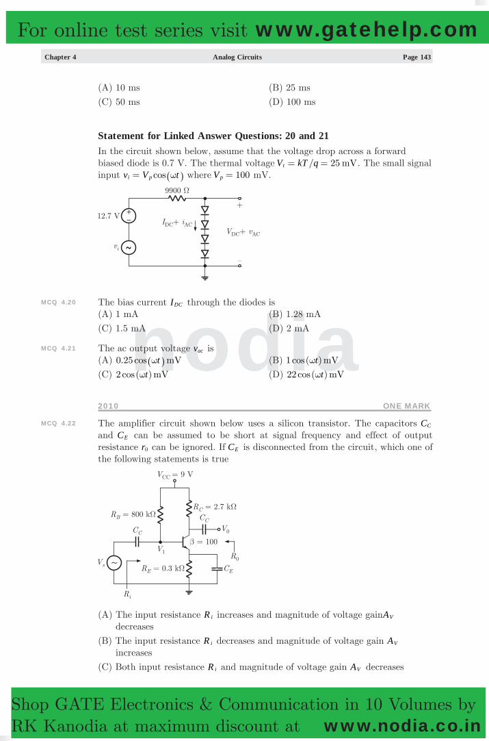
Chapter 4 Analog Circuits Page 143
nodia
Shop GATE Electronics & Communication in 10 Volumes by RK Kanodia at maximum discount at www.nodia.co.in
For online test series visit www.gatehelp.com
(A) 10 ms (B) 25 ms
(C) 50 ms (D) 100 ms
Statement for Linked Answer Questions: 20 and 21In the circuit shown below, assume that the voltage drop across a forward biased diode is 0.7 V. The thermal voltage / 25 mVV kT qt = = . The small signal input cosv V ti p w= ^ h where V 100p = mV.
MCQ 4.20 The bias current IDC through the diodes is(A) 1 mA (B) 1.28 mA
(C) 1.5 mA (D) 2 mA
MCQ 4.21 The ac output voltage vac is(A) 0.25cos mVtw^ h (B) 1 ( )cos mVtw(C) 2 ( )cos mVtw (D) 22 ( )cos mVtw
2010 ONE MARK
MCQ 4.22 The amplifier circuit shown below uses a silicon transistor. The capacitors CC and CE can be assumed to be short at signal frequency and effect of output resistance r0 can be ignored. If CE is disconnected from the circuit, which one of the following statements is true
(A) The input resistance Ri increases and magnitude of voltage gainAV decreases
(B) The input resistance Ri decreases and magnitude of voltage gain AV increases
(C) Both input resistance Ri and magnitude of voltage gain AV decreases

Page 144 Analog Circuits Chapter 4
nodia
Shop GATE Electronics & Communication in 10 Volumes by RK Kanodia at maximum discount at www.nodia.co.in
For online test series visit www.gatehelp.com
(D) Both input resistance Ri and the magnitude of voltage gain AV increases
MCQ 4.23 In the silicon BJT circuit shown below, assume that the emitter area of transistor Q1 is half that of transistor Q2
The value of current Io is approximately(A) 0.5 mA (B) 2 mA
(C) 9.3 mA (D) 15 mA
MCQ 4.24 Assuming the OP-AMP to be ideal, the voltage gain of the amplifier shown below is
(A) RR
1
2- (B) RR
1
3-
(C) ||R
R R1
2 3- (D) RR R
1
2 3- +b l
2010 TWO MARKS
Common Data For Q. 25 and 26 Consider the common emitter amplifier shown below with the following circuit parameters:
100, 0.3861 / , 259 , 1 , 93 ,A V k kg r R Rm S B0b W W W= = = = =250 , 1 , 4.7k k and FR R C CC L 1 23 mW W= = = =

Chapter 4 Analog Circuits Page 145
nodia
Shop GATE Electronics & Communication in 10 Volumes by RK Kanodia at maximum discount at www.nodia.co.in
For online test series visit www.gatehelp.com
MCQ 4.25 The resistance seen by the source vS is(A) 258 W (B) 1258 W(C) 93 kW (D) 3
MCQ 4.26 The lower cut-off frequency due to C2 is(A) 33.9 Hz
(B) 27.1 Hz
(C) 13.6 Hz
(D) 16.9 Hz
MCQ 4.27 The transfer characteristic for the precision rectifier circuit shown below is (assume ideal OP-AMP and practical diodes)
2009 TWO MARKS
MCQ 4.28 In the circuit below, the diode is ideal. The voltage V is given by
(A) min ( , )V 1i (B) max ( , )V 1i
(C) min ( , )V 1i- (D) max ( , )V 1i-
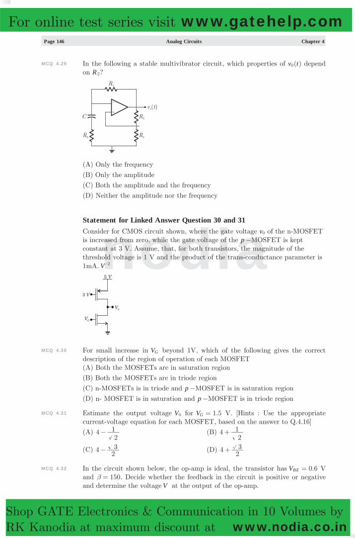
Page 146 Analog Circuits Chapter 4
nodia
Shop GATE Electronics & Communication in 10 Volumes by RK Kanodia at maximum discount at www.nodia.co.in
For online test series visit www.gatehelp.com
MCQ 4.29 In the following a stable multivibrator circuit, which properties of ( )v t0 depend on R2?
(A) Only the frequency
(B) Only the amplitude
(C) Both the amplitude and the frequency
(D) Neither the amplitude nor the frequency
Statement for Linked Answer Question 30 and 31Consider for CMOS circuit shown, where the gate voltage v0 of the n-MOSFET is increased from zero, while the gate voltage of the p -MOSFET is kept constant at 3 V. Assume, that, for both transistors, the magnitude of the threshold voltage is 1 V and the product of the trans-conductance parameter is 1mA. V 2-
MCQ 4.30 For small increase in VG beyond 1V, which of the following gives the correct description of the region of operation of each MOSFET(A) Both the MOSFETs are in saturation region
(B) Both the MOSFETs are in triode region
(C) n-MOSFETs is in triode and p -MOSFET is in saturation region
(D) n- MOSFET is in saturation and p -MOSFET is in triode region
MCQ 4.31 Estimate the output voltage V0 for .V 1 5G = V. [Hints : Use the appropriate current-voltage equation for each MOSFET, based on the answer to Q.4.16]
(A) 42
1- (B) 42
1+
(C) 423- (D) 4
23+
MCQ 4.32 In the circuit shown below, the op-amp is ideal, the transistor has .V 0 6BE = V and 150b = . Decide whether the feedback in the circuit is positive or negative and determine the voltage V at the output of the op-amp.

Chapter 4 Analog Circuits Page 147
nodia
Shop GATE Electronics & Communication in 10 Volumes by RK Kanodia at maximum discount at www.nodia.co.in
For online test series visit www.gatehelp.com
(A) Positive feedback, V 10= V(B) Positive feedback, V 0= V(C) Negative feedback, V 5= V(D) Negative feedback, V 2= V
MCQ 4.33 A small signal source ( ) cos sinV t A t B t20 10i6= + is applied to a transistor
amplifier as shown below. The transistor has 150b = and h 3ie W= . Which expression best approximate ( )V t0
(A) ( ) ( )cos sinV t A t B t1500 20 1006=- +
(B) ( ) 1500( 20 10 )cos sinV t A t B t06
= +-(C) ( ) sinV t B t1500 100
6=-(D) ( ) sinV t B t150 100
6=-
2008 ONE MARK
MCQ 4.34 In the following limiter circuit, an input voltage sinV t10 100i p= is applied. Assume that the diode drop is 0.7 V when it is forward biased. When it is forward biased. The zener breakdown voltage is 6.8 VThe maximum and minimum values of the output voltage respectively are
(A) 6.1 , 0.7V V- (B) 0.7 , 7.5V V-(C) 7.5 , 0.7V V- (D) 7.5 , 7.5V V-

Page 148 Analog Circuits Chapter 4
nodia
Shop GATE Electronics & Communication in 10 Volumes by RK Kanodia at maximum discount at www.nodia.co.in
For online test series visit www.gatehelp.com
2008 TWO MARSK
MCQ 4.35 For the circuit shown in the following figure, transistor M1 and M2 are identical NMOS transistors. Assume the M2 is in saturation and the output is unloaded.
The current Ix is related to Ibias as(A) I I Ix bias s= + (B) I Ix bias=
(C) I I VRV
x bias DDE
out= - -c m (D) I I Ix bias s= -
MCQ 4.36 Consider the following circuit using an ideal OPAMP. The I-V characteristic of
the diode is described by the relation I I eVV
01
t= -_ i where V 25T = mV, I 10 m= A and V is the voltage across the diode (taken as positive for forward bias). For an input voltage 1 VVi =- , the output voltage V0 is
(A) 0 V (B) 0.1 V
(C) 0.7 V (D) 1.1 V
MCQ 4.37 The OPAMP circuit shown above represents a
(A) high pass filter
(B) low pass filter
(C) band pass filter
(D) band reject filter
MCQ 4.38 Two identical NMOS transistors M1 and M2 are connected as shown below. Vbias is chosen so that both transistors are in saturation. The equivalent gm of the pair
is defied to be VI
i
out
22 at constant Vout
The equivalent gm of the pair is

Chapter 4 Analog Circuits Page 149
nodia
Shop GATE Electronics & Communication in 10 Volumes by RK Kanodia at maximum discount at www.nodia.co.in
For online test series visit www.gatehelp.com
(A) the sum of individual 'gm s of the transistors
(B) the product of individual gm ’s of the transistors
(C) nearly equal to the gm of M1
(D) nearly equal to ggm
0 of M2
MCQ 4.39 Consider the Schmidt trigger circuit shown belowA triangular wave which goes from -12 to 12 V is applied to the inverting input of OPMAP. Assume that the output of the OPAMP swings from +15 V to -15 V. The voltage at the non-inverting input switches between
(A) V12- to +12 V (B) -7.5 V to 7.5 V
(C) -5 V to +5 V (D) 0 V and 5 V
Statement for Linked Answer Question 40 and 41In the following transistor circuit, .V 0 7BE = V, r 253 = mV/IE , and b and all the capacitances are very large
MCQ 4.40 The value of DC current IE is(A) 1 mA (B) 2 mA
(C) 5 mA (D) 10 mA
MCQ 4.41 The mid-band voltage gain of the amplifier is approximately(A) -180 (B) -120
(C) -90 (D) -60

Page 150 Analog Circuits Chapter 4
nodia
Shop GATE Electronics & Communication in 10 Volumes by RK Kanodia at maximum discount at www.nodia.co.in
For online test series visit www.gatehelp.com
2007 ONE MARK
MCQ 4.42 The correct full wave rectifier circuit is
MCQ 4.43 In a transconductance amplifier, it is desirable to have(A) a large input resistance and a large output resistance
(B) a large input resistance and a small output resistance
(C) a small input resistance and a large output resistance
(D) a small input resistance and a small output resistance
2007 TWO MARKS
MCQ 4.44 For the Op-Amp circuit shown in the figure, V0 is
(A) -2 V (B) -1 V
(C) -0.5 V (D) 0.5 V
MCQ 4.45 For the BJT circuit shown, assume that the b of the transistor is very large and .V 0 7BE = V. The mode of operation of the BJT is
(A) cut-off (B) saturation
(C) normal active (D) reverse active
MCQ 4.46 In the Op-Amp circuit shown, assume that the diode current follows the equation ( / )expI I V Vs T= . For ,V V V V2i 0 01= = , and for ,V V V V4i 0 02= = .
The relationship between V01 and V02 is

Chapter 4 Analog Circuits Page 151
nodia
Shop GATE Electronics & Communication in 10 Volumes by RK Kanodia at maximum discount at www.nodia.co.in
For online test series visit www.gatehelp.com
(A) V V2 o02 1= (B) V e Vo o22
1=(C) 1V V n2o o2 1= (D) 1V V V n2o o T1 2 =-
MCQ 4.47 In the CMOS inverter circuit shown, if the trans conductance parameters of the NMOS and PMOS transistors are
kn kp= /CLW C
LW
A V40n oxn
nox
p
p 2m m m= = =
and their threshold voltages ae V V 1THn THp= = V the current I is
(A) 0 A (B) 25 mA
(C) 45 mA (D) 90 mA
MCQ 4.48 For the Zener diode shown in the figure, the Zener voltage at knee is 7 V, the knee current is negligible and the Zener dynamic resistance is 10 W. If the input voltage ( )Vi range is from 10 to 16 V, the output voltage ( )V0 ranges from
(A) 7.00 to 7.29 V (B) 7.14 to 7.29 V
(C) 7.14 to 7.43 V (D) 7.29 to 7.43 V
Statement for Linked Answer Questions 49 and 50:Consider the Op-Amp circuit shown in the figure.
MCQ 4.49 The transfer function ( )/ ( )V s V si0 is
(A) sRCsRC
11+- (B)
sRCsRC
11-+

Page 152 Analog Circuits Chapter 4
nodia
Shop GATE Electronics & Communication in 10 Volumes by RK Kanodia at maximum discount at www.nodia.co.in
For online test series visit www.gatehelp.com
(C) sRC11
- (D)
sRC11
+
MCQ 4.50 If ( )sinV V ti 1 w= and ( )sinV V t0 2 w f= + , then the minimum and maximum values of f (in radians) are respectively
(A) 2p- and
2p (B) 0 and
2p
(C) p- and 0 (D) 2p- and 0
2006 ONE MARK
MCQ 4.51 The input impedance ( )Zi and the output impedance ( )Z0 of an ideal trans-conductance (voltage controlled current source) amplifier are(A) ,Z Z0 0i 0= =
(B) ,Z Z0i 0 3= =(C) ,Z Z 0i 03= =
(D) ,Z Zi 03 3= =
MCQ 4.52 An n-channel depletion MOSFET has following two points on its I VD Gs- curve:(i) V 0GS = at I 12D = mA and(ii) V 6GS =- Volts at I 0D = mAWhich of the following Q point will given the highest trans conductance gain for small signals?(A) V 6GS =- Volts (B) V 3GS =- Volts
(C) V 0GS = Volts (D) V 3GS = Volts
2006 TWO MARKS
MCQ 4.53 For the circuit shown in the following figure, the capacitor C is initially uncharged. At t 0= the switch S is closed. The Vc across the capacitor at t 1= millisecond isIn the figure shown above, the OP-AMP is supplied with V15! .
(A) 0 Volt (B) 6.3 Volt
(C) 9.45 Volts (D) 10 Volts
MCQ 4.54 For the circuit shown below, assume that the zener diode is ideal with a breakdown voltage of 6 volts. The waveform observed across R is

Chapter 4 Analog Circuits Page 153
nodia
Shop GATE Electronics & Communication in 10 Volumes by RK Kanodia at maximum discount at www.nodia.co.in
For online test series visit www.gatehelp.com
Common Data For Q. 55 to 57In the transistor amplifier circuit shown in the figure below, the transistor has the following parameters:
DCb 60= , . ,V V h0 7BE ie " 3=The capacitance CC can be assumed to be infinite.
In the figure above, the ground has been shown by the symbol 4
MCQ 4.55 Under the DC conditions, the collector-or-emitter voltage drop is(A) 4.8 Volts (B) 5.3 Volts
(C) 6.0 Volts (D) 6.6 Volts
MCQ 4.56 If DCb is increased by 10%, the collector-to-emitter voltage drop(A) increases by less than or equal to 10%
(B) decreases by less than or equal to 10%
(C) increase by more than 10%
(D) decreases by more than 10%
MCQ 4.57 The small-signal gain of the amplifier vv
s
c is(A) -10 (B) -5.3
(C) 5.3 (D) 10
Common Data For Q. 58 and 59A regulated power supply, shown in figure below, has an unregulated input (UR) of 15 Volts and generates a regulated output Vout . Use the component values shown in the figure.

Page 154 Analog Circuits Chapter 4
nodia
Shop GATE Electronics & Communication in 10 Volumes by RK Kanodia at maximum discount at www.nodia.co.in
For online test series visit www.gatehelp.com
MCQ 4.58 The power dissipation across the transistor Q1 shown in the figure is(A) 4.8 Watts (B) 5.0 Watts
(C) 5.4 Watts (D) 6.0 Watts
MCQ 4.59 If the unregulated voltage increases by 20%, the power dissipation across the transistor Q1(A) increases by 20% (B) increases by 50%
(C) remains unchanged (D) decreases by 20%
2005 ONE MARK
MCQ 4.60 The input resistance Ri of the amplifier shown in the figure is
(A) k430 W (B) 10 kW
(C) 40 kW (D) infinite
MCQ 4.61 The effect of current shunt feedback in an amplifier is to(A) increase the input resistance and decrease the output resistance
(B) increases both input and output resistance
(C) decrease both input and output resistance
(D) decrease the input resistance and increase the output resistance
MCQ 4.62 The cascade amplifier is a multistage configuration of(A) CC CB- (B) CE CB-(C) CB CC- (D) CE CC-
2005 TWO MARKS
MCQ 4.63 In an ideal differential amplifier shown in the figure, a large value of ( )RE .(A) increase both the differential and common - mode gains.
(B) increases the common mode gain only.
(C) decreases the differential mode gain only.
(D) decreases the common mode gain only.

Chapter 4 Analog Circuits Page 155
nodia
Shop GATE Electronics & Communication in 10 Volumes by RK Kanodia at maximum discount at www.nodia.co.in
For online test series visit www.gatehelp.com
MCQ 4.64 For an npn transistor connected as shown in figure .V 0 7BE = volts. Given that reverse saturation current of the junction at room temperature 300 K is 10 13- A, the emitter current is
(A) 30 mA (B) 39 mA
(C) 49 mA (D) 20 mA
MCQ 4.65 The voltage e0 is indicated in the figure has been measured by an ideal voltmeter. Which of the following can be calculated ?
(A) Bias current of the inverting input only
(B) Bias current of the inverting and non-inverting inputs only
(C) Input offset current only
(D) Both the bias currents and the input offset current
MCQ 4.66 The Op-amp circuit shown in the figure is filter. The type of filter and its cut. Off frequency are respectively
(A) high pass, 1000 rad/sec. (B) Low pass, 1000 rad/sec
(C) high pass, 1000 rad/sec (D) low pass, 10000 rad/sec
MCQ 4.67 The circuit using a BJT with 50b = and .V V0 7BE = is shown in the figure. The base current IB and collector voltage by VC and respectively

Page 156 Analog Circuits Chapter 4
nodia
Shop GATE Electronics & Communication in 10 Volumes by RK Kanodia at maximum discount at www.nodia.co.in
For online test series visit www.gatehelp.com
(A) 43 mA and 11.4 Volts (B) 40 mA and 16 Volts
(C) 45 mA and 11 Volts (D) 50 mA and 10 Volts
MCQ 4.68 The Zener diode in the regulator circuit shown in the figure has a Zener voltage of 5.8 volts and a zener knee current of 0.5 mA. The maximum load current drawn from this current ensuring proper functioning over the input voltage range between 20 and 30 volts, is
(A) 23.7 mA (B) 14.2 mA
(C) 13.7 mA (D) 24.2 mA
MCQ 4.69 Both transistors T1 and T2 show in the figure, have a 100b = , threshold voltage of 1 Volts. The device parameters K1 and K2 of T1 and T2 are, respectively, 36 /A V2m and 9 mA/V2. The output voltage Vo i s
(A) 1 V (B) 2 V
(C) 3 V (D) 4 V
Common Data For Q. 70 to 72Given, r k20d W= , I 10DSS = mA, V 8p =- V
MCQ 4.70 Zi and Z0 of the circuit are respectively
(A) 2 MW and 2 kW (B) 2 MW and 1120 kW
(C) infinity and 2 MW (D) infinity and 1120 kW
MCQ 4.71 ID and VDS under DC conditions are respectively(A) 5.625 mA and 8.75 V (B) 1.875 mA and 5.00 V
(C) 4.500 mA and 11.00 V (D) 6.250 mA and 7.50 V

Chapter 4 Analog Circuits Page 157
nodia
Shop GATE Electronics & Communication in 10 Volumes by RK Kanodia at maximum discount at www.nodia.co.in
For online test series visit www.gatehelp.com
MCQ 4.72 Transconductance in milli-Siemens (mS) and voltage gain of the amplifier are respectively(A) 1.875 mS and 3.41
(B) 1.875 ms and -3.41
(C) 3.3 mS and -6
(D) 3.3 mS and 6
MCQ 4.73 Given the ideal operational amplifier circuit shown in the figure indicate the correct transfer characteristics assuming ideal diodes with zero cut-in voltage.
2004 ONE MARK
MCQ 4.74 An ideal op-amp is an ideal(A) voltage controlled current source
(B) voltage controlled voltage source
(C) current controlled current source
(D) current controlled voltage source
MCQ 4.75 Voltage series feedback (also called series-shunt feedback) results in(A) increase in both input and output impedances
(B) decrease in both input and output impedances
(C) increase in input impedance and decrease in output impedance
(D) decrease in input impedance and increase in output impedance

Page 158 Analog Circuits Chapter 4
nodia
Shop GATE Electronics & Communication in 10 Volumes by RK Kanodia at maximum discount at www.nodia.co.in
For online test series visit www.gatehelp.com
MCQ 4.76 The circuit in the figure is a
(A) low-pass filter (B) high-pass filter
(C) band-pass filter (D) band-reject filter
2004 TWO MARKS
MCQ 4.77 A bipolar transistor is operating in the active region with a collector current of 1 mA. Assuming that the b of the transistor is 100 and the thermal voltage ( )VT is 25 mV, the transconductance ( )gm and the input resistance ( )rp of the transistor in the common emitter configuration, are(A) g 25m = mA/V and 15.625 kr W=p (B) g 40m = mA/V and .r 4 0=p kW(C) g 25m = mA/V and .r 2 5=p k W (D) g 40m = mA/V and .r 2 5=p kW
MCQ 4.78 The value of C required for sinusoidal oscillations of frequency 1 kHz in the circuit of the figure is
(A) 21p
mF (B) 2p mF
(C) 2 6
1p
mF (D) 2 6p mF
MCQ 4.79 In the op-amp circuit given in the figure, the load current iL is
(A) RVs
2- (B)
RVs
2

Chapter 4 Analog Circuits Page 159
nodia
Shop GATE Electronics & Communication in 10 Volumes by RK Kanodia at maximum discount at www.nodia.co.in
For online test series visit www.gatehelp.com
(C) RV
L
s- (D) RVs
1
MCQ 4.80 In the voltage regulator shown in the figure, the load current can vary from 100 mA to 500 mA. Assuming that the Zener diode is ideal (i.e., the Zener knee current is negligibly small and Zener resistance is zero in the breakdown region), the value of R is
(A) 7 W (B) 70W
(C) 370 W (D) 14 W
MCQ 4.81 In a full-wave rectifier using two ideal diodes, Vdc and Vm are the dc and peak values of the voltage respectively across a resistive load. If PIV is the peak inverse voltage of the diode, then the appropriate relationships for this rectifier are
(A) , 2V V PIV Vdcm
mp= = (B) 2 , 2I V PIV Vdc
mmp
= =
(C) 2 ,V V PIV Vdcm
mp= = (D) ,V V PIV Vdc
mmp
=
MCQ 4.82 Assume that the b of transistor is extremely large and . ,V V I0 7BE C= and VCE in the circuit shown in the figure
(A) 1 , 4.7mA VI VC CE= = (B) .I 0 5C = mA, .V 3 75CE = V
(C) I 1C = mA, .V 2 5CE = V (D) .I 0 5C = mA, .V 3 9CE = V
2003 ONE MARK
MCQ 4.83 Choose the correct match for input resistance of various amplifier configurations shown below :Configuration Input resistanceCB : Common Base LO : LowCC : Common Collector MO : ModerateCE : Common Emitter HI : High(A) CB LO, CC MO, CE HI- - -(B) CB LO, CC HI, CE MO- - -(C) CB MO, CC HI, CE LO- - -(D) CB HI, CC LO, CE MO- - -
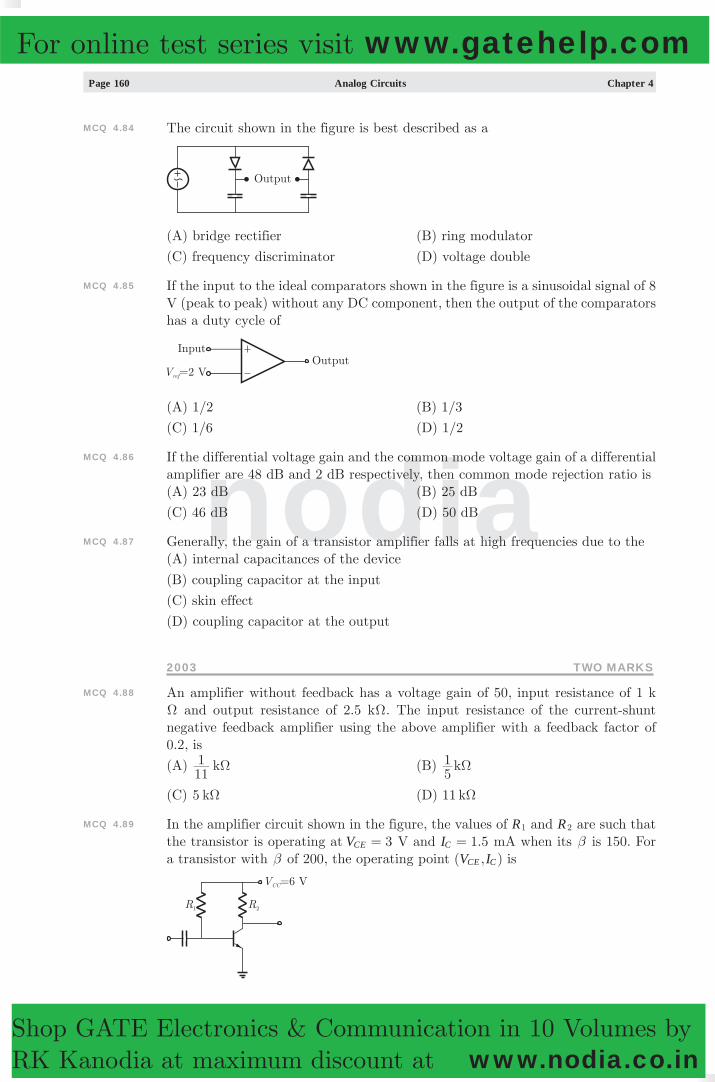
Page 160 Analog Circuits Chapter 4
nodia
Shop GATE Electronics & Communication in 10 Volumes by RK Kanodia at maximum discount at www.nodia.co.in
For online test series visit www.gatehelp.com
MCQ 4.84 The circuit shown in the figure is best described as a
(A) bridge rectifier (B) ring modulator
(C) frequency discriminator (D) voltage double
MCQ 4.85 If the input to the ideal comparators shown in the figure is a sinusoidal signal of 8 V (peak to peak) without any DC component, then the output of the comparators has a duty cycle of
(A) 1/2 (B) 1/3
(C) 1/6 (D) 1/2
MCQ 4.86 If the differential voltage gain and the common mode voltage gain of a differential amplifier are 48 dB and 2 dB respectively, then common mode rejection ratio is(A) 23 dB (B) 25 dB
(C) 46 dB (D) 50 dB
MCQ 4.87 Generally, the gain of a transistor amplifier falls at high frequencies due to the (A) internal capacitances of the device
(B) coupling capacitor at the input
(C) skin effect
(D) coupling capacitor at the output
2003 TWO MARKS
MCQ 4.88 An amplifier without feedback has a voltage gain of 50, input resistance of 1 k W and output resistance of 2.5 kW. The input resistance of the current-shunt negative feedback amplifier using the above amplifier with a feedback factor of 0.2, is
(A) k111 W (B) k
51 W
(C) 5 kW (D) 11 kW
MCQ 4.89 In the amplifier circuit shown in the figure, the values of R1 and R2 are such that the transistor is operating at 3VCE = V and .I 1 5C = mA when its b is 150. For a transistor with b of 200, the operating point ( , )V ICE C is

Chapter 4 Analog Circuits Page 161
nodia
Shop GATE Electronics & Communication in 10 Volumes by RK Kanodia at maximum discount at www.nodia.co.in
For online test series visit www.gatehelp.com
(A) (2 V, 2 mA) (B) (3 V, 2 mA)
(C) (4 V, 2 mA) (D) (4 V, 1 mA)
MCQ 4.90 The oscillator circuit shown in the figure has an ideal inverting amplifier. Its frequency of oscillation (in Hz) is
(A) ( )RC2 6
1p
(B) ( )RC2
1p
(C) ( )RC6
1 (D) ( )RC2
6p
MCQ 4.91 The output voltage of the regulated power supply shown in the figure is
(A) 3 V (B) 6 V
(C) 9 V (D) 12 V
MCQ 4.92 If the op-amp in the figure is ideal, the output voltage Vout will be equal to
(A) 1 V (B) 6 V
(C) 14 V (D) 17 V
MCQ 4.93 Three identical amplifiers with each one having a voltage gain of 50, input resistance of 1 kW and output resistance of 250 W are cascaded. The opened circuit voltages gain of the combined amplifier is(A) 49 dB (B) 51 dB
(C) 98 dB (D) 102 dB

Page 162 Analog Circuits Chapter 4
nodia
Shop GATE Electronics & Communication in 10 Volumes by RK Kanodia at maximum discount at www.nodia.co.in
For online test series visit www.gatehelp.com
MCQ 4.94 An ideal sawtooth voltages waveform of frequency of 500 Hz and amplitude 3 V is generated by charging a capacitor of 2 mF in every cycle. The charging requires(A) Constant voltage source of 3 V for 1 ms
(B) Constant voltage source of 3 V for 2 ms
(C) Constant voltage source of 1 mA for 1 ms
(D) Constant voltage source of 3 mA for 2 ms
2002 ONE MARK
MCQ 4.95 In a negative feedback amplifier using voltage-series (i.e. voltage-sampling, series mixing) feedback.(A) Ri decreases and R0 decreases (B) Ri decreases and R0 increases
(C) Ri increases and R0 decreases (D) Ri increases and R0 increases
(Ri and R0 denote the input and output resistance respectively)
MCQ 4.96 A 741-type opamp has a gain-bandwidth product of 1 MHz. A non-inverting amplifier suing this opamp and having a voltage gain of 20 dB will exhibit a -3 dB bandwidth of(A) 50 kHz (B) 100 kHz
(C) 17
1000 kHz (D) .7 07
1000 kHz
MCQ 4.97 Three identical RC-coupled transistor amplifiers are cascaded. If each of the amplifiers has a frequency response as shown in the figure, the overall frequency response is as given in

Chapter 4 Analog Circuits Page 163
nodia
Shop GATE Electronics & Communication in 10 Volumes by RK Kanodia at maximum discount at www.nodia.co.in
For online test series visit www.gatehelp.com
2002 TWO MARKS
MCQ 4.98 The circuit in the figure employs positive feedback and is intended to generate
sinusoidal oscillation. If at a frequency , ( )( )( )
,f B fV fV f
61 0f
00
3 c+= = then to sustain oscillation at this frequency
(A) R R52 1= (B) R R62 1=
(C) R R621= (D) R R
521=
MCQ 4.99 An amplifier using an opamp with a slew-rate SR 1= /V m sec has a gain of 40 dB. If this amplifier has to faithfully amplify sinusoidal signals from dc to 20 kHz without introducing any slew-rate induced distortion, then the input signal level must not exceed.(A) 795 mV (B) 395 mV
(C) 79.5 mV (D) 39.5 mV
MCQ 4.100 A zener diode regulator in the figure is to be designed to meet the specifications: 10IL = mA 10V0 = V and Vin varies from 30 V to 50 V. The zener diode has 10Vz = V and Izk (knee current) =1 mA. For satisfactory operation
(A) R 1800# W (B) R2000 2200# #W W(C) R3700 4000# #W W (D) R 4000$ W
MCQ 4.101 The voltage gain Avv
vt
0= of the JFET amplifier shown in the figure is I 10DSS = mA 5Vp =- V(Assume ,C C1 2 and Cs to be very large
(A) +16 (B) -16
(C) +8 (D) -6

Page 164 Analog Circuits Chapter 4
nodia
Shop GATE Electronics & Communication in 10 Volumes by RK Kanodia at maximum discount at www.nodia.co.in
For online test series visit www.gatehelp.com
2001 ONE MARK
MCQ 4.102 The current gain of a BJT is
(A) g rm 0 (B) rgm
(C) g rm p (D) rgm
p
MCQ 4.103 Thee ideal OP-AMP has the following characteristics.(A) , , 0R A Ri 03 3= = =
(B) 0, , 0R A Ri 03= = =(C) , ,R A Ri 03 3 3= = =
(D) 0, ,R A Ri 03 3= = =
MCQ 4.104 Consider the following two statements :Statement 1 :A stable multi vibrator can be used for generating square wave.Statement 2:Bistable multi vibrator can be used for storing binary information.(A) Only statement 1 is correct
(B) Only statement 2 is correct
(C) Both the statements 1 and 2 are correct
(D) Both the statements 1 and 2 are incorrect
2001 TWO MARKS
MCQ 4.105 An npn BJT has g 38m = mA/V, 10C 14=m- F, 4 10C 13
#=p- F, and DC current
gain 900b = . For this transistor fT and fb are(A) .f 1 64 10T
8#= Hz and .f 1 47 1010#=b Hz
(B) .f 1 47 10T10#= Hz and .f 1 64 108#=b Hz
(C) .f 1 33 10T12#= Hz and .f 1 47 1010#=b Hz
(D) .f 1 47 10T10#= Hz and .f 1 33 1012#=b Hz
MCQ 4.106 The transistor shunt regulator shown in the figure has a regulated output voltage of 10 V, when the input varies from 20 V to 30 V. The relevant parameters for the zener diode and the transistor are : .V 9 5z = , .V 0 3BE = V, 99b = , Neglect the current through RB . Then the maximum power dissipated in the zener diode ( )Pz and the transistor ( )PT are
(A) P 75z = mW, .P 7 9T = W
(B) P 85z = mW, .P 8 9T = W
(C) P 95z = mW, .P 9 9T = W
(D) P 115z = mW, .P 11 9T = W

Chapter 4 Analog Circuits Page 165
nodia
Shop GATE Electronics & Communication in 10 Volumes by RK Kanodia at maximum discount at www.nodia.co.in
For online test series visit www.gatehelp.com
MCQ 4.107 The oscillator circuit shown in the figure is
4
(A) Hartely oscillator with .f 79 6oscillation = MHz
(B) Colpitts oscillator with .f 50 3oscillation = MHz
(C) Hartley oscillator with .f 159 2oscillation = MHz
(D) Colpitts oscillator with .f 159 3oscillation = MHz
MCQ 4.108 The inverting OP-AMP shown in the figure has an open-loop gain of 100.
The closed-loop gain VV
s
0 is(A) 8- (B) 9-(C) 10- (D) 11-
MCQ 4.109 In the figure assume the OP-AMPs to be ideal. The output v0 of the circuit is
(A) ( )cos t10 100 (B) ( )cos d10 100t
0t t#
(C) ( )cos d10 100t4
0t t- # (D) ( )cos
dtd t10 1004-
2000 ONE MARK
MCQ 4.110 Introducing a resistor in the emitter of a common amplifier stabilizes the dc operating point against variations in(A) only the temperature (B) only the b of the transistor
(C) both temperature and b (D) none of the above
MCQ 4.111 In the differential amplifier of the figure, if the source resistance of the current

Page 166 Analog Circuits Chapter 4
nodia
Shop GATE Electronics & Communication in 10 Volumes by RK Kanodia at maximum discount at www.nodia.co.in
For online test series visit www.gatehelp.com
source IEE is infinite, then the common-mode gain is
(A) zero (B) infinite
(C) indeterminate (D) V
V V2 T
in in1 2+
MCQ 4.112 In the circuit of the figure, V0 is
(A) -1 V (B) 2 V
(C) +1 V (D) +15 V
MCQ 4.113 The current gain of a bipolar transistor drops at high frequencies because of(A) transistor capacitances (B) high current effects in the base
(C) parasitic inductive elements (D) the Early effect
MCQ 4.114 If the op-amp in the figure, is ideal, then v0 is
(A) zero (B) ( )sinV V t1 2 w-(C) ( )sinV V t1 2 w- + (D) ( )sinV V t1 2 w+
MCQ 4.115 The configuration of the figure is a

Chapter 4 Analog Circuits Page 167
nodia
Shop GATE Electronics & Communication in 10 Volumes by RK Kanodia at maximum discount at www.nodia.co.in
For online test series visit www.gatehelp.com
(A) precision integrator (B) Hartely oscillator
(C) Butterworth high pass filter (D) Wien-bridge oscillator
MCQ 4.116 Assume that the op-amp of the figure is ideal. If vi is a triangular wave, then v0 will be
(A) square wave (B) triangular wave
(C) parabolic wave (D) sine wave
MCQ 4.117 The most commonly used amplifier is sample and hold circuits is(A) a unity gain inverting amplifier
(B) a unity gain non-inverting amplifier
(C) an inverting amplifier with a gain of 10
(D) an inverting amplifier with a gain of 100
2000 TWO MARKS
MCQ 4.118 In the circuit of figure, assume that the transistor is in the active region. It has a large b and its base-emitter voltage is 0.7 V. The value of Ic is
(A) Indeterminate since Rc is not given (B) 1 mA
(C) 5 mA (D) 10 mA
MCQ 4.119 If the op-amp in the figure has an input offset voltage of 5 mV and an open-loop voltage gain of 10000, then v0 will be
(A) 0 V (B) 5 mV
(C) + 15 V or -15 V (D) +50 V or -50 V

Page 168 Analog Circuits Chapter 4
nodia
Shop GATE Electronics & Communication in 10 Volumes by RK Kanodia at maximum discount at www.nodia.co.in
For online test series visit www.gatehelp.com
1999 ONE MARK
MCQ 4.120 The first dominant pole encountered in the frequency response of a compensated op-amp is approximately at(A) 5 Hz (B) 10 kHz
(C) 1MHz (D) 100 MHz
MCQ 4.121 Negative feedback in an amplifier(A) reduces gain
(B) increases frequency and phase distortions
(C) reduces bandwidth
(D) increases noise
MCQ 4.122 In the cascade amplifier shown in the given figure, if the common-emitter stage ( )Q1 has a transconductance gm1, and the common base stage ( )Q2 has a transconductance gm2, then the overall transconductance ( / )g i vi0= of the cascade amplifier is
(A) gm1 (B) gm2
(C) g2m1
(D) g2m2
MCQ 4.123 Crossover distortion behavior is characteristic of(A) Class A output stage (B) Class B output stage
(C) Class AB output stage (D) Common-base output stage
1999 TWO MARK
MCQ 4.124 An amplifier has an open-loop gain of 100, an input impedance of 1 kW,and an output impedance of 100W. A feedback network with a feedback factor of 0.99 is connected to the amplifier in a voltage series feedback mode. The new input and output impedances, respectively, are(A) 10 1andW W (B) 10 10and kW W(C) 100 1andkW W (D) 100 k and k1W W
MCQ 4.125 A dc power supply has a no-load voltage of 30 V, and a full-load voltage of 25 V at a full-load current of 1 A. Its output resistance and load regulation, respectively, are(A) 5 20%andW (B) 25 20%andW(C) 5 16.7%andW (D) 25 16.7%andW
1998 ONE MARK
MCQ 4.126 The circuit of the figure is an example of feedback of the following type

Chapter 4 Analog Circuits Page 169
nodia
Shop GATE Electronics & Communication in 10 Volumes by RK Kanodia at maximum discount at www.nodia.co.in
For online test series visit www.gatehelp.com
(A) current series (B) current shunt
(C) voltage series (D) voltage shunt
MCQ 4.127 In a differential amplifier, CMRR can be improved by using an increased(A) emitter resistance (B) collector resistance
(C) power supply voltages (D) source resistance
MCQ 4.128 From a measurement of the rise time of the output pulse of an amplifier whose is a small amplitude square wave, one can estimate the following parameter of the amplifier(A) gain-bandwidth product (B) slow rate
(C) upper 3–dB frequency (D) lower 3–dB frequency
MCQ 4.129 The emitter coupled pair of BJT’s given a linear transfer relation between the differential output voltage and the differential output voltage and the differential input voltage Vid is less a times the thermal voltage, where a is(A) 4 (B) 3
(C) 2 (D) 1
MCQ 4.130 In a shunt-shunt negative feedback amplifier, as compared to the basic amplifier(A) both, input and output impedances,decrease
(B) input impedance decreases but output impedance increases
(C) input impedance increase but output
(D) both input and output impedances increases.
1998 TWO MARKS
MCQ 4.131 A multistage amplifier has a low-pass response with three real poles at ands 1 2 3w w w=- - . The approximate overall bandwidth B of the amplifier will
be given by
(A) B 1 2 3w w w= + + (B) B1 1 1 1
1 2 3w w w= + +
(C) ( )B /1 2 3
1 3w w w= + + (D) B 12
22
32w w w= + +
MCQ 4.132 One input terminal of high gain comparator circuit is connected to ground and a sinusoidal voltage is applied to the other input. The output of comparator will be(A) a sinusoid (B) a full rectified sinusoid
(C) a half rectified sinusoid (D) a square wave
MCQ 4.133 In a series regulated power supply circuit, the voltage gain Av of the ‘pass’ transistor satisfies the condition(A) Av " 3 (B) A1 << <v 3
(C) A 1v . (D) A 1<<v

Page 170 Analog Circuits Chapter 4
nodia
Shop GATE Electronics & Communication in 10 Volumes by RK Kanodia at maximum discount at www.nodia.co.in
For online test series visit www.gatehelp.com
MCQ 4.134 For full wave rectification, a four diode bridge rectifier is claimed to have the following advantages over a two diode circuit :(A) less expensive transformer,
(B) smaller size transformer, and
(C) suitability for higher voltage application.
Of these,
(A) only (1) and (2) are true (B) only (1) and (3) are true
(C) only (2) and (3) are true (D) (1), (2) as well as (3) are true
MCQ 4.135 In the MOSFET amplifier of the figure is the signal output V1 and V2 obey the relationship
(A) V V212= (B) V V
212=-
(C) V V21 2= (D) V V21 2=-
MCQ 4.136 For small signal ac operation, a practical forward biased diode can be modelled as(A) a resistance and a capacitance in series
(B) an ideal diode and resistance in parallel
(C) a resistance and an ideal diode in series
(D) a resistance
1997 ONE MARK
MCQ 4.137 In the BJT amplifier shown in the figure is the transistor is based in the forward active region. Putting a capacitor across RE will
(A) decrease the voltage gain and decrease the input impedance
(B) increase the voltage gain and decrease the input impedance
(C) decrease the voltage gain and increase the input impedance

Chapter 4 Analog Circuits Page 171
nodia
Shop GATE Electronics & Communication in 10 Volumes by RK Kanodia at maximum discount at www.nodia.co.in
For online test series visit www.gatehelp.com
(D) increase the voltage gain and increase the input impedance
MCQ 4.138 A cascade amplifier stags is equivalent to(A) a common emitter stage followed by a common base stage
(B) a common base stage followed by an emitter follower
(C) an emitter follower stage followed by a common base stage
(D) a common base stage followed by a common emitter stage
MCQ 4.139 In a common emitter BJT amplifier, the maximum usable supply voltage is limited by(A) Avalanche breakdown of Base-Emitter junction
(B) Collector-Base breakdown voltage with emitter open ( )BVCBO
(C) Collector-Emitter breakdown voltage with base open ( )BVCBO
(D) Zener breakdown voltage of the Emitter-Base junction
1997 TWO MARKS
MCQ 4.140 In the circuit of in the figure is the current iD through the ideal diode (zero cut in voltage and forward resistance) equals
(A) 0 A (B) 4 A
(C) 1 A (D) None of the above
MCQ 4.141 The output voltage V0 of the circuit shown in the figure is
(A) 4 V- (B) 6 V
(C) 5 V (D) 5.5 V-
MCQ 4.142 A half wave rectifier uses a diode with a forward resistance Rf . The voltage is sinV tm w and the load resistance is RL . The DC current is given by
(A) R
V2 L
m (B) ( )R R
Vf L
m
p +
(C) V2 m
p (D) R
VL
m

Page 172 Analog Circuits Chapter 4
nodia
Shop GATE Electronics & Communication in 10 Volumes by RK Kanodia at maximum discount at www.nodia.co.in
For online test series visit www.gatehelp.com
1996 ONE MARK
MCQ 4.143 In the circuit of the given figure, assume that the diodes are ideal and the meter is an average indicating ammeter. The ammeter will read
(A) 0.4 A2 (B) 0.4 A
(C) . A0 8p (D) . mamp0 4
pMCQ 4.144 The circuit shown in the figure is that of
(A) a non-inverting amplifier (B) an inverting amplifier
(C) an oscillator (D) a Schmitt trigger
1996 TWO MARKS
MCQ 4.145 In the circuit shown in the given figure N is a finite gain amplifier with a gain of k , a very large input impedance, and a very low output impedance. The input impedance of the feedback amplifier with the feedback impedance Z connected as shown will be
(A) Z k1 1-b l (B) ( )Z k1 -
(C) ( )k
Z1- (D)
( )kZ
1 -MCQ 4.146 A Darlington stage is shown in the figure. If the transconductance of Q1 is gm1 and
Q2 is gm2, then the overall transconductance gvi
mcbeccc
T; E is given by

Chapter 4 Analog Circuits Page 173
nodia
Shop GATE Electronics & Communication in 10 Volumes by RK Kanodia at maximum discount at www.nodia.co.in
For online test series visit www.gatehelp.com
(A) gm1 (B) . g0 5 m1
(C) gm2 (D) . g0 5 m2
MCQ 4.147 Value of R in the oscillator circuit shown in the given figure, so chosen that it just oscillates at an angular frequency of w. The value of w and the required value of R will respectively be
(A) 10 / , 2 10secrad5 4 W# (B) / , 2 10secrad2 104 4# W#
(C) 2 10 / ,10secrad4 5 W# (D) 10 / ,10secrad5 5 W
MCQ 4.148 A zener diode in the circuit shown in the figure is has a knee current of 5 mA, and a maximum allowed power dissipation of 300 mW. What are the minimum and maximum load currents that can be drawn safely from the circuit, keeping the output voltage V0 constant at 6 V?
(A) 0 , 180mA mA (B) 5 , 110mA mA
(C) 10 , 55mA mA (D) 60 ,180mA mA
***********

Page 174 Analog Circuits Chapter 4
nodia
Shop GATE Electronics & Communication in 10 Volumes by RK Kanodia at maximum discount at www.nodia.co.in
For online test series visit www.gatehelp.com
SOLUTIONS
SOL 4.1 Option (B) is correct.For the given ideal op-amp, negative terminal will be also ground (at zero voltage) and so, the collector terminal of the BJT will be at zero voltage.
i.e., VC 0 volt=The current in 1 kW resistor is given by
I 1 k5 0
W= - 5 mA=
This current will flow completely through the BJT since, no current will flow
into the ideal op-amp ( /I P resistance of ideal op-amp is infinity). So, for BJT
we have
VC 0= VB 0= IC 5 mA=i.e.,the base collector junction is reverse biased (zero voltage) therefore, the
collector current (IC ) can have a value only if base-emitter is forward biased.
Hence, VBE 0.7 volts=& V VB E- .0 7=& V0 out- .0 7=or, Vout 0.7 volt=-
SOL 4.2 Option (A) is correct.The /i p voltage of the system is given as
Vin V Vf1= + V kVout1= + V k A V1 0 1= + V A Vout 0 1=^ h
V k A11 0= +^ h
Therefore, if k is increased then input voltage is also increased so, the input
impedance increases. Now, we have
Vout A V0 1= Ak A
V1
in0
0=
+^ h
k AA V
1in
0
0=+^ h
Since, Vin is independent of k when seen from output mode, the output voltage decreases with increase in k that leads to the decrease of output impedance. Thus, input impedance increases and output impedance decreases.
SOL 4.3 Option (A) is correct.For the given circuit, we obtain the small signal model as shown in figure below :

Chapter 4 Analog Circuits Page 175
nodia
Shop GATE Electronics & Communication in 10 Volumes by RK Kanodia at maximum discount at www.nodia.co.in
For online test series visit www.gatehelp.com
We obtain the node voltage at V1 as
RV
R sC
V g V1DL
m i1 1+
++ 0=
& V1
R R sC
g V1
11
DL
m i=+
+
-
Therefore, the output voltage V0 is obtained as
V0 R sC
V R1
L
L1=+
R sC
R
R R sC
g V1 1
11
L
L
DL
m i=+ +
+
-J
L
KKK
N
P
OOO
so, the transfer function is
VV
i
0 sC R RR R sCg
1 D L
D L m=+ +-
^ h
Then, we have the pole at C R R
1D L
w =+^ h
It gives the lower cutoff frequency of transfer function.
i.e., 0w C R R
1D L
=+^ h
or, f0 C R R21D Lp
=+^ h
2 10 20 10
16 3
# # #p= -
.7 97= 8 Hz.
SOL 4.4 Option (B) is correct.
From the circuit, we have
Is I IZ L= +or, IZ I Is L= - (1)Since, voltage across zener diode is 5 V so, current through 100W resistor is obtained as
Is 0.05 A10010 5= - =
Therefore, the load current is given by
IL R5
L=
Since, for proper operation, we must have IZ Iknes$So, from Eq. (1), we write
0.05 A R5
L- 10 mA$
50 mA R5
L- 10 mA$

Page 176 Analog Circuits Chapter 4
nodia
Shop GATE Electronics & Communication in 10 Volumes by RK Kanodia at maximum discount at www.nodia.co.in
For online test series visit www.gatehelp.com
40 mA R5
L$
40 10 3#
- R5
L$
140 10 3
#- R
5L#
40 10
53
#- RL#
or, 125W RL#Therefore, minimum value of 125RL W=Now, we know that power rating of Zener diode is given by PR V I maxZ Z= ^ h
I maxZ^ h is maximum current through zener diode in reverse bias. Maximum currrent through zener diode flows when load current is zero. i.e.,
I maxZ^ h .I 10010 5 0 05s= = - =
Therefore, PR 5 0.05 W#= 250 mW=
SOL 4.5 Option (C) is correct.
For the given ideal op-Amps we can assume
V2- V V2 2= =+ (ideal)
V1+ V V1 1= =- (ideal)
So, by voltage division
V1 V
21out#=
Vout V2 1=and, as the I/P current in Op-amp is always zero therefore, there will be no voltage drop across 1 KW in II op-amp i.e., V2 1 V=Therefore,
V V1
1 2- V
122=
- -^ h
& V 11- 1 2= +or, V1 4=Hence, Vout 2 8 voltV1= =
SOL 4.6 Option (B) is correct.For the given circuit, we can make the truth table as below

Chapter 4 Analog Circuits Page 177
nodia
Shop GATE Electronics & Communication in 10 Volumes by RK Kanodia at maximum discount at www.nodia.co.in
For online test series visit www.gatehelp.com
X Y Z0011
0101
0100
Logic 0 means voltage is 0 voltv = and logic 1 means voltage is 5 volt
For x 0= , y 0= , Transistor is at cut off mode and diode is forward biased. Since, there is no drop across forward biased diode. So, Z Y 0= =For x 0= , y 1= , Again Transistor is in cutoff mode, and diode is forward biased. with no current flowing through resistor. So, Z Y 1= =For x 1= , y 0= , Transistor is in saturation mode and so, z directly connected to ground irrespective of any value of Y .i.e., Z 0= (ground)Similarly for X Y 1= = Z 0= (ground)Hence, from the obtained truth table, we get Z X Y=
SOL 4.7 Option (D) is correct.Given, the input voltage VYZ sin t100 w=
For ve+ half cycle VYZ 0>i.e., VY is a higher voltage than VZ
So, the diode will be in cutoff region. Therefore, there will no voltage difference between X and W node.i.e., VWX 0=Now, for ve- half cycle all the four diodes will active and so, X and W terminal is short circuitedi.e., VWX 0= Hence, VWX 0= for all t
SOL 4.8 Option (C) is correct.The equivalent circuit can be shown as

Page 178 Analog Circuits Chapter 4
nodia
Shop GATE Electronics & Communication in 10 Volumes by RK Kanodia at maximum discount at www.nodia.co.in
For online test series visit www.gatehelp.com
VTh V R RR
CC1 2
2= + R RR3
1 2
2= +
and RTh R RR R2 1
2 1= +Since, I IC Bb= has 3.b (very high) so, IB is negative in comparison to IC . Therefore, we can write the base voltage
VB VTh=So, 0.7V I RTh C E- - 0=
or, 0.7R RR3 10 500
1 2
2 3
+ - - -^ ^h h 0=
or, 60 k RR3
2
2
W+ . .0 7 0 5= +
or, R3 2 60 . 1.2k R1 2 2W= +^ ^h h
or, . R1 8 2 60 .k 1 2W #= ^ ^h h
Hence, R2 .. 40 k1 8
60 1 2# W= =
SOL 4.9 Option (D) is correct.Let 0.7 Vv > and diode is forward biased. By applying Kirchoff’s voltage law
10 1ki v#- - 0=
. ( )v v10 5000 7 1000- - -: D 0=
10 ( 0.7) 2v v#- - - 0= .v10 3 1 4- + 0=
v . 3.8 > .V311 4 0 7= = (Assumption is true)
So, .i v500
0 7= - . . 6.2 mA5003 8 0 7= - =
SOL 4.10 Option (C) is correct.
Given ib 1 0.1 (1000 )cos mAtp= +So, IB = DC component of ib
1 mA=In small signal model of the transistor
rp IVC
Tb= VT " Thermal voltage
/I
VIV
C
T
B
T
b= = IV
B
T= I ICBb =
So, rp 125 25mA
mV W= = ,mV mAV I25 1T B= =
SOL 4.11 Option (A) is correct.The circuit composed of a clamper and a peak rectifier as shown.

Chapter 4 Analog Circuits Page 179
nodia
Shop GATE Electronics & Communication in 10 Volumes by RK Kanodia at maximum discount at www.nodia.co.in
For online test series visit www.gatehelp.com
Clamper clamps the voltage to zero voltage, as shown
The peak rectifier adds 1+ V to peak voltage, so overall peak voltage lowers down by 1- volt.
So, vo 1cos tw= -
SOL 4.12 Option (A) is correct.We put a test source between terminal 1, 2 to obtain equivalent impedance
ZTh IV
test
test=
Applying KCL at top right node
9 1 99k kV V I100
test testb+ + - Itest=
99kV V I10 100
test testb+ - Itest= ...(i)
But Ib 10kk kV V
9 1test test=- + =-
Substituting Ib into equation (i), we have
10 10k kV V V
10099test test test+ + Itest=
V V10 10100
100test test
3#
+ Itest=
V1002 test Itest=
ZTh 50IV
test
test W= =
SOL 4.13 Option (B) is correct.First we obtain the transfer function.

Page 180 Analog Circuits Chapter 4
nodia
Shop GATE Electronics & Communication in 10 Volumes by RK Kanodia at maximum discount at www.nodia.co.in
For online test series visit www.gatehelp.com
( ) ( )
j C R
V jRV j
10 0i o
12
w
w w
+
- + - 0=
( )R
V jo
2
w
( )
j C R
V j1
i
1w
w=+
-
( )V jo w ( )
R j C
V j R1
i
1
2
w
w=--
At 0"w (Low frequencies), C1w ," 3 so V 0o =
At " 3w (higher frequencies)
C1w ,0" so ( ) ( )V j R
R V jo i1
2w w=-
The filter passes high frequencies so it is a high pass filter.
( )H jw VV
R j C
R1i
o
1
2
w= =
--
( )H 3 RR
RR
1
2
1
2= - =
At 3 dB frequency, gain will be 2 times of maximum gain ( )H 36 @
H j 0w^ h ( )H2
1 3=
So, R
C
R1
12
02 2
2
w+
RR
21
1
2= b l
R2 12 R
C1
12
02 2w
= +
R12
C12 2w
=
0w R C11
=
SOL 4.14 Option (D) is correct.DC Analysis :
Using KVL in input loop,

Chapter 4 Analog Circuits Page 181
nodia
Shop GATE Electronics & Communication in 10 Volumes by RK Kanodia at maximum discount at www.nodia.co.in
For online test series visit www.gatehelp.com
.V I100 0 7C B- - 0= VC .I100 0 7B= + ...(i)
IC . ( )I kV I12
13 7 1EC
B- b= - = +
. V12 1013 7 C
3#
- I100 B= ...(ii)
Solving equation (i) and (ii),
IB 0.01 mA=Small Signal Analysis :Transforming given input voltage source into equivalent current source.
This is a shunt-shunt feedback amplifier.Given parameters,
rp 0.0125 2.5mA
mV kIV
B
T W= = =
gm . 0.04 sr 2 5 1000100#
b= = =p
Writing KCL at output node
Rv g v R
v vC
mF
0 0+ + -p
p 0=
v R R v g R1 1 1C F
mF
0 + + -p: :D D 0=
Substituting 1 ,kR 2C W= 100 ,kRF W= 0.04 sgm = (9.33 10 ) (0.04)v v0
5# + p
- 0= v0 . V428 72=- p ...(i)Writing KCL at input node
Rv
s
i Rv
rv
Rv v
s F
o= + + -p
p
p p
Rv
s
i v R r R Rv1 1 1
s F F
0= + + -pp
: D
Rv
s
i (5.1 10 )v Rv
F
4 0#= -p-
Substituting Vp from equation (i)
Rv
s
i .. v R
v428 72
5 1 10F
4
00#= - -
-
v10 10
i3
# 1.16 10 1 10v v6
05
0# #=- -- - 10 kRs W= (source resistance)
v10 10
i3
# .1 116 10 5
#=- -
Av .
8.96vv
10 10 1 116 101
i
03 5
# # #-= = -
SOL 4.15 Option (A) is correct.

Page 182 Analog Circuits Chapter 4
nodia
Shop GATE Electronics & Communication in 10 Volumes by RK Kanodia at maximum discount at www.nodia.co.in
For online test series visit www.gatehelp.com
For the parallel RLC circuit resonance frequency is,
rw LC1
10 10 1 1016 9
# # #= =
- - 10 /M rad s=
Thus given frequency is resonance frequency and parallel RLC circuit has maximum impedance at resonance frequency
Gain of the amplifier is ( )g Z Rm C L# where ZC is impedance of parallel RLC
circuit.
At rw w= , 2 kZ R Z maxC CW= = = .Hence at this frequency ( )rw , gain is
Gainrw w= ( ) (2 2 )k kg Z R g g 10m C L m m
3#= = = which is maximum.
Therefore gain is maximum at 10 / secM radrw = .
SOL 4.16 Option (D) is correct.The given circuit is shown below :
From diagram we can write
Ii RV
sLVo o
1 1= +
Transfer function
( )H s IV
R sLsR Lo
1 1 1
1 1= = +
or ( )H jw R j Lj R L1 1
1 1
ww= +
At 0w = ( ) 0H jw =At 3w = ( ) tancons tH j R1w = = . Hence HPF.
SOL 4.17 Option (C) is correct.Given circuit is shown below.
For transistor M2,
VGS V V V V0G S x x= - = - = VDS V V V V0D S x x= - = - =

Chapter 4 Analog Circuits Page 183
nodia
Shop GATE Electronics & Communication in 10 Volumes by RK Kanodia at maximum discount at www.nodia.co.in
For online test series visit www.gatehelp.com
Since V VGS T- V V1 <x DS= - , thus M2 is in saturation.By assuming M1 to be in saturation we have
I ( )DS M1 I ( )DS M2=
( )( )C V2 4 5 1n xx
0 2m - - ( )C V2 1 1n xx
0 2m= -
( )V4 4 x2- ( )V 1x
2= -or ( )V2 4 x- ( )V 1x!= -Taking positive root, V8 2 x- V 1x= - Vx 3 V=At 3 VVx = for , 5 3 2 VM V V<GS DS1 = - = . Thus our assumption is true and
3 VVx = .
SOL 4.18 Option (D) is correct.
We have a .0 98=
Now b .1 4 9aa= - =
In active region, for common emitter amplifier,
IC (1 )I IB COb b= + + ...(1)
Substituting ICO 0.6 Am= and 20 AIB m= in above eq we have,
IC 1.01 mA=
SOL 4.19 Option (C) is correct.
In active region V onBE 0.7 V=Emitter voltage VE 5.7 VV V onB BE= - =-
Emitter Current IE 4.3( )
4.3. ( )
1k k mAV 10 5 7 10E= - - = - - - =
Now IC 1 mAIE. =Applying KCL at collector
i1 0.5 mA=
Since i1 C dtdVC=
or VC C i dt Ci t1
11= =# ...(1)
with time, the capacitor charges and voltage across collector changes from 0 towards negative.
When saturation starts, VCE 0.7 5 VVC&= =+ (across capacitor)

Page 184 Analog Circuits Chapter 4
nodia
Shop GATE Electronics & Communication in 10 Volumes by RK Kanodia at maximum discount at www.nodia.co.in
For online test series visit www.gatehelp.com
Thus from (1) we get, 5+ .AmA T5
0 5m=
or T .0 5 10
5 5 103
6
## #= -
- 50 secm=
SOL 4.20 Option (A) is correct.The current flows in the circuit if all the diodes are forward biased. In forward biased there will be .0 7 V drop across each diode.
Thus IDC . ( . )
1 mA990012 7 4 0 7= - =
SOL 4.21 Option (B) is correct.The forward resistance of each diode is
r 125
mAmV
IV 25
C
T W= = =
Thus Vac ( )( )
Vr
r4 9900
4i #= +e o
100 ( ) .cosmV t 0 01w=
1 ( )cos mVtw=
SOL 4.22 Option (A) is correct.The equivalent circuit of given amplifier circuit (when CE is connected, RE is short-circuited)
Input impedance Ri ||R rB= p
Voltage gain AV g Rm C=Now, if CE is disconnected, resistance RE appears in the circuit
Input impedance Rin || [ ( )]R r R1B Eb= + +p
Input impedance increases
Voltage gain AV g Rg R
1 m E
m C= + Voltage gain decreases.
SOL 4.23 Option (B) is correct.Since, emitter area of transistor Q1 is half of transistor Q2, so current
IE 1 andI I I21
21
E B B2 1 2= =
The circuit is as shown below :

Chapter 4 Analog Circuits Page 185
nodia
Shop GATE Electronics & Communication in 10 Volumes by RK Kanodia at maximum discount at www.nodia.co.in
For online test series visit www.gatehelp.com
VB 10 ( 0.7) 9.3 V=- - - =-
Collector current I1 (9.3 )( . )
1k
mA0 9 3
W= - - =
1b 700= (high), So I IC E 1.
Applying KCL at base we have
I1 E- I IB B1 2= + ( )I1 1 B1 1b- + I IB B1 2= +
1 ( ) I I700 1 1 2B
B2
2= + + +
IB 2 7022.
I IC0 2= IB2 2:b= 715 7022
#= 2 mA.
SOL 4.24 Option (A) is correct.The circuit is as shown below :
So, RV
RV0 0i o
1 2
- + - 0=
or VV
i
o RR
1
2=-
SOL 4.25 Option (B) is correct.By small signal equivalent circuit analysis
Input resistance seen by source vs
Rin ||iv R R r
s
ss s s= = + (1000 ) (93 || 259 ) 1258kW W W W= + =

Page 186 Analog Circuits Chapter 4
nodia
Shop GATE Electronics & Communication in 10 Volumes by RK Kanodia at maximum discount at www.nodia.co.in
For online test series visit www.gatehelp.com
SOL 4.26 Option (B) is correct.Cut-off frequency due to C2
fo ( )R R C21
C L 2p= +
. .
271 Hz2 3 14 1250 4 7 10
16
# # # #= =-
Lower cut-off frequency fL f10
o. 27.1 Hz10271= =
SOL 4.27 Option (B) is correct.The circuit is as shown below
Current I R RV
RV
420 0 0 5i i= - + - = +
If ,I 0> diode D2 conducts
So, for ,V V D25 0 5> >I
I 2&+ - conducts
Equivalent circuit is shown below
Output is V 0o = . If I 0< , diode D2 will be off
RV5 I+ ,V D0 5< <I 2& - is off
The circuit is shown below
RV
R RV0
40 20 0i o- + - + - 0=
or Vo 5Vi=- -
At V 5i =- V, Vo 0=At V 10i =- V, Vo 5 V=

Chapter 4 Analog Circuits Page 187
nodia
Shop GATE Electronics & Communication in 10 Volumes by RK Kanodia at maximum discount at www.nodia.co.in
For online test series visit www.gatehelp.com
SOL 4.28 Option (A) is correct.Let diode be OFF. In this case 1 A current will flow in resistor and voltage across resistor will be 1V = .VDiode is off, it must be in reverse biased, therefore V V1 0 1> >i i"-Thus for V 1>i diode is off and V V1=Option (B) and (C) doesn’t satisfy this condition.Let V 1<i . In this case diode will be on and voltage across diode will be zero and V Vi=Thus V ( , )min V 1i=
SOL 4.29 Option (A) is correct.The R2 decide only the frequency.
SOL 4.30 Option (D) is correct.For small increase in VG beyond 1 V the n - channel MOSFET goes into saturation as V iveGS "+ and p - MOSFET is always in active region or triode region.
SOL 4.31 Option (C) is correct.
SOL 4.32 Option (D) is correct.The circuit is shown in fig below
The voltage at non inverting terminal is 5 V because OP AMP is ideal and inverting terminal is at 5 V.
Thus IC k5
10 5 1= - = mA
VE I RE E= . .m k V1 1 4 1 4#= = I IE C= . . V0 6 1 4 2= + =Thus the feedback is negative and output voltage is V V2= .
SOL 4.33 Option (D) is correct.The output voltage is
V0 A Vr i= h
h RV
ie
fe Ci.-
Here 3RC W= and 3 khie W=
Thus V0 3150 3
kk Vi.
#-
( )cos sinA t B t150 20 106.- +
Since coupling capacitor is large so low frequency signal will be filtered out, and
best approximation is

Page 188 Analog Circuits Chapter 4
nodia
Shop GATE Electronics & Communication in 10 Volumes by RK Kanodia at maximum discount at www.nodia.co.in
For online test series visit www.gatehelp.com
V0 sinB t150 106.-
SOL 4.34 Option (C) is correct.For the positive half of Vi , the diode D1 is forward bias, D2 is reverse bias and the zener diode is in breakdown state because .V 6 8>i .Thus output voltage is
V0 0.7 6.8 7.5= + = V
For the negative half of ,V Di 2 is forward bias thus
Then V0 .0 7=- V
SOL 4.35 Option (B) is correct.By Current mirror,
Ix IL
WL
W
bias
1
2=^
^
h
h
Since MOSFETs are identical,
Thus LW
2b l L
W2
= b l
Hence Ix Ibias=
SOL 4.36 Option (B) is correct.The circuit is using ideal OPAMP. The non inverting terminal of OPAMP is at ground, thus inverting terminal is also at virtual ground.
Thus current will flow from -ive terminal (0 Volt) to -1 Volt source. Thus the current I is
I ( )
k k1000 1
1001= - - =
The current through diode is
I I e 1VV
0 t= -_ i
Now V 25T = mV and 1I0 = mA
Thus I 10 e 1101V6
25 10 53= - =#
- -8 B
or V .0 06= V
Now V0 4kI V#= + .k
k100
1 4 0 06#= + 0.1= V
SOL 4.37 Option (B) is correct.The circuit is using ideal OPAMP. The non inverting terminal of OPAMP is at ground, thus inverting terminal is also at virtual ground.Thus we can write
R sL
vi
1+ v
sR CR
12 2
2
= -+
or vv
i
0 ( )( )R sL sR C
R11 2 2
2=-+ +

Chapter 4 Analog Circuits Page 189
nodia
Shop GATE Electronics & Communication in 10 Volumes by RK Kanodia at maximum discount at www.nodia.co.in
For online test series visit www.gatehelp.com
and from this equation it may be easily seen that this is the standard form of
T.F. of low pass filter
( )H s ( )( )R sL sR C
K11 2 2
=+ +
and form this equation it may be easily seen that this is the standard form of
T.F. of low pass filter
( )H s as bs b
K2=+ +
SOL 4.38 Option (C ) is correct.The current in both transistor are equal. Thus gm is decide by M1.
SOL 4.39 Option (C) is correct.Let the voltage at non inverting terminal be V1, then after applying KCL at non inverting terminal side we have
V V V10
1510
1 0 1- + - ( )V10
151= - -
or V1 V30=
If V0 swings from -15 to +15 V then V1 swings between -5 V to +5 V.
SOL 4.40 Option (A) is correct.For the given DC values the Thevenin equivalent circuit is as follows
The Thevenin resistance and voltage are
VTH 9 310 20
10 #=+
= V
and total RTH 10 2010 20
k kk k#=+
.6 67= kW
Since b is very large, therefore IB is small and can be ignored
Thus IE .
.R
V Vk2 3
3 0 7 1E
TH BE= - = - = mA
SOL 4.41 Option (D) is correct.The small signal model is shown in fig below

Page 190 Analog Circuits Chapter 4
nodia
Shop GATE Electronics & Communication in 10 Volumes by RK Kanodia at maximum discount at www.nodia.co.in
For online test series visit www.gatehelp.com
gm 251
VI
251
mm
T
C= = = A/V I IC E.
Vo ( )g V k k3 3m #=- p
( . )V k251 1 5in=- V Vin=p
V60 in=-
or Am VV 60
in
o= =-
SOL 4.42 Option (C) is correct.The circuit shown in (C) is correct full wave rectifier circuit.
SOL 4.43 Option (A) is correct.In the transconductance amplifier it is desirable to have large input resistance and large output resistance.
SOL 4.44 Option (C) is correct.We redraw the circuit as shown in fig.
Applying voltage division rule
v+ .0 5= V
We know that v+ v= -
Thus v- .0 5= V
Now i . .k1
1 0 5 0 5= - = mA
and i . .k
v2
0 5 0 50= - = mA
or v0 . .0 5 1 0 5= - =- V
SOL 4.45 Option (B) is correct.If we assume b very large, then I 0B = and I IE C= ; .V 0 7BE = V. We assume that

Chapter 4 Analog Circuits Page 191
nodia
Shop GATE Electronics & Communication in 10 Volumes by RK Kanodia at maximum discount at www.nodia.co.in
For online test series visit www.gatehelp.com
BJT is in active, so applying KVL in Base-emitter loop
IE R
V2E
BE= - . .k1
2 0 7 1 3= - = mA
Since b is very large, we have I IE C= , thus
IC .1 3= mA
Now applying KVL in collector-emitter loop
I V I10 10 C CE C- - - 0=or VCE .4 3=- V
Now VBC V VBE CE= - . ( . )0 7 4 3 5= - - = V
Since .V 0 7>BC V, thus transistor in saturation.
SOL 4.46 Option (D) is correct.Here the inverting terminal is at virtual ground and the current in resistor and diode current is equal i.e.
IR ID=
or RVi I e /
sV VD T=
or VD 1VI RVnTs
i=
For the first condition
VD 0 1V VI R2no Ts
1= =-
For the first condition
VD 0 1V VI R4no Ts
1= =-
Subtracting above equation
V Vo o1 2- 1 1VI R
VI R
4 2n nTs
Ts
= -
or V Vo o1 2- 1 1V V24n n2T T= =
SOL 4.47 Option (D) is correct.
We have Vthp V 1thp= = V
and LW
P
P 40LW A/V
N
N 2= = m
From figure it may be easily seen that Vas for each NMOS and PMOS is 2.5 V
Thus ID ( )K V Vas T2= - ( . )40 2 5 1
VA 22
m= - 90 m= A
SOL 4.48 Option (C) is correct.We have V 7Z = volt, ,V R0 10K Z W= =Circuit can be modeled as shown in fig below

Page 192 Analog Circuits Chapter 4
nodia
Shop GATE Electronics & Communication in 10 Volumes by RK Kanodia at maximum discount at www.nodia.co.in
For online test series visit www.gatehelp.com
Since Vi is lies between 10 to 16 V, the range of voltage across 200 kW V200 V V 3i Z= - = to 9 volt
The range of current through 200 kW is
k200
3 15= mA to k200
9 45= mA
The range of variation in output voltage
15 0.15Rm Z# = V to 45 0.45Rm Z# =
Thus the range of output voltage is 7.15 Volt to 7.45 Volt
SOL 4.49 Option (A) is correct.The voltage at non-inverting terminal is
V+ R
VsCR
V1
1sC
sCi i1
1
=+
=+
Now V- VsCR
V1
1i= =
++
Applying voltage division rule
V+ ( )( )
R RR V V
V V2i
o i
1 1
10=
++ = +
or sCR
V1
1i+
( )V V2
o i= +
or VV
i
o sRC
11
2=- ++
VV
i
0 sRCsRC
11=+-
SOL 4.50 Option (C) is correct.
VV
i
0 ( )H ssRCsRC
11= =+-
( )H jw j RCj RC
11
ww=
+-
( )H j+ w tan tanRC RC1 1f w w= =- -- -
tan RC2 2w=- -
Minimum value, minf ( )at " 3= p w-Maximum value, maxf 0( 0)at= =w
SOL 4.51 Option (D) is correct.In the transconductance amplifier it is desirable to have large input impedance and large output impedance.
SOL 4.52 Option (C) is correct.
SOL 4.53 Option (D) is correct.The voltage at inverting terminal is
V- V 10= =+ V
Here note that current through the capacitor is constant and that is
I 1 1 10k kV 10= = =- mA
Thus the voltage across capacitor at t 1= msec is
VC C
Idt mdt111 10
m m
0
1
0
1
m= =# # dt10 10
Im4
0= =# V

Chapter 4 Analog Circuits Page 193
nodia
Shop GATE Electronics & Communication in 10 Volumes by RK Kanodia at maximum discount at www.nodia.co.in
For online test series visit www.gatehelp.com
SOL 4.54 Option (A) is correct.In forward bias Zener diode works as normal diode.Thus for negative cycle of input Zener diode is forward biased and it conducts giving V VR in= .For positive cycle of input Zener diode is reversed biasedwhen V0 6< <in , Diode is OFF and V 0R =when V 6>in Diode conducts and voltage across diode is 6 V. Thus voltage across is resistor is
VR V 6in= -Only option (B) satisfy this condition.
SOL 4.55 Option (C) is correct.The circuit under DC condition is shown in fig below
Applying KVL we have
( )V R I I VCC C C B CE- + - 0= ...(1)
and V R I VCC B B BE- - 0= ...(2)Substituting I IC Bb= in (1) we have
( )V R I I VCC C B B CEb- + - 0= ...(3)
Solving (2) and (3) we get
VCE
( )
V
RR
V V
11
CC
C
B
CC BE
b
= -+
+
- ...(4)
Now substituting values we get
VCE
( )
.121
1 1 6053
12 0 7= -+
+ +
- .5 95= V
SOL 4.56 Option (B) is correct.
We have 'b 100110 60 66#= =
Substituting ' 66b = with other values in (iv) in previous solutions
VCE
( )
.121
1 1 6653
12 0 7= -+
+ +
- .5 29= V
Thus change is .
. .5 95
5 29 59 5 100#= - . %4 3=-
SOL 4.57 Option (A) is correct.
SOL 4.58 Option (C) is correct.The Zener diode is in breakdown region, thus
V+ V 6Z= = V Vin=

Page 194 Analog Circuits Chapter 4
nodia
Shop GATE Electronics & Communication in 10 Volumes by RK Kanodia at maximum discount at www.nodia.co.in
For online test series visit www.gatehelp.com
We know that Vo VRR
1inf
1= +c m
or Vout Vkk6 1
2412 9o= = + =` j V
The current in 12 kW branch is negligible as comparison to 10 W. Thus Current
I IC E. . .R
V109 0 9
L
out= = = A
Now VCE 15 9 6= - = V
The power dissipated in transistor is
P V ICE C= . .6 0 9 5 4#= = W
SOL 4.59 Option (B) is correct.If the unregulated voltage increase by 20%, them the unregulated voltage is 18 V, but the V V 6Z in= = remain same and hence Vout and IC remain same. There will be change in VCE
Thus, VCE 18 9 9- - = V
IC 0.9= A
Power dissipation P V ICE C= .9 0 9#= .8 1= W
Thus % increase in power is
.
. .5 4
8 1 5 4 100#- %50=
SOL 4.60 Option (B) is correct.Since the inverting terminal is at virtual ground, the current flowing through the voltage source is
Is 10V
ks=
or IV
s
s 10 Rk inW= =
SOL 4.61 Option (D) is correct.The effect of current shunt feedback in an amplifier is to decrease the input resistance and increase the output resistance as :
Rif AR
1i
b=
+
Rof ( )R A10 b= +where Ri " Input resistance without feedback
Rif " Input resistance with feedback.
SOL 4.62 Option (B) is correct.The CE configuration has high voltage gain as well as high current gain. It performs basic function of amplifications. The CB configuration has lowest Ri and highest Ro . It is used as last step to match a very low impedance source and to drain a high impedance loadThus cascade amplifier is a multistage configuration of CE-CB
SOL 4.63 Option (D) is correct.Common mode gain
ACM RR2 E
C=-
And differential mode gain

Chapter 4 Analog Circuits Page 195
nodia
Shop GATE Electronics & Communication in 10 Volumes by RK Kanodia at maximum discount at www.nodia.co.in
For online test series visit www.gatehelp.com
ADM g Rm C=-Thus only common mode gain depends on RE and for large value of RE it
decreases.
SOL 4.64 Option (C) is correct.
IE I e 1s nVV
T
BE
= -` j .e
10 0 7 1 491 26
1310 3= - =
# #
--c m mA
SOL 4.65 Option (C) is correct.The circuit is as shown below
Writing equation for I- have
e V1M
0 - - I= -
or e0 (1I M) V= +- - ...(1)
Writing equation for I+ we have
1
V0M- + I= +
or V+ (1I M)=- + ...(2)
Since for ideal OPAMP V V=+ -, from (1) and (2) we have
e0 (1 (1I M) I M)= -- +
( )(1I I M)= -- + (1I M)OS=
Thus if e0 has been measured, we can calculate input offset current IOS only.
SOL 4.66 Option (C) is correct.At low frequency capacitor is open circuit and voltage acr s non-inverting terminal is zero. At high frequency capacitor act as short circuit and all input voltage appear at non-inverting terminal. Thus, this is high pass circuit.The frequency is given by
w RC1=
1 10 1 101 1000
3 6# # #= =- rad/sec
SOL 4.67 Option (B) is correct.The circuit under DC condition is shown in fig below

Page 196 Analog Circuits Chapter 4
nodia
Shop GATE Electronics & Communication in 10 Volumes by RK Kanodia at maximum discount at www.nodia.co.in
For online test series visit www.gatehelp.com
Applying KVL we have
V R I V R ICC B B BE E E- - - 0=or ( )V R I V R I1CC B B BE E Bb- - - + 0= Since I I IE B Bb= +
or IB ( )R R
V V1B E
CC BE
b=
+ +-
430 (50 1)1
.20 0 7k k+ +
= - 40m= A
Now IC I 50 40 2B #b m= = = mA
VC V R ICC C C= - 20 2 2 16m k#= =- V
SOL 4.68 Option (A) is correct.The maximum load current will be at maximum input voltage i.e.
Vmax 30= V i.e.
1
V Vk
max Z- I IL Z= +
or 1
.30 5 8k
- .I 0 5L= = m
or IL . . .24 2 0 5 23 7= - = mA
SOL 4.69 Option (D) is correct.
SOL 4.70 Option (B) is correct.The small signal model is as shown below
From the figure we have
Zin 2 MW=
and Z0 r Rd D= 20 2k k= 1120 kW=
SOL 4.71 Option (A) is correct.The circuit in DC condition is shown below
Since the FET has high input resistance, gate current can be neglect and we get VGS 2=- V
Since V V 0< <P GS , FET is operating in active region

Chapter 4 Analog Circuits Page 197
nodia
Shop GATE Electronics & Communication in 10 Volumes by RK Kanodia at maximum discount at www.nodia.co.in
For online test series visit www.gatehelp.com
Now ID IVV1DSS
P
GS 2= -c m
( )( )
10 182 2
= ---
c m .5 625= mA
Now VDS V I RDD D D= - .20 5 625= - m 2# k .8 75= V
SOL 4.72 Option (B) is correct.The transconductance is
gm V I I
2P D DSS
=
or, 5.625 1082 mA mA#= .1 875= mS
The gain is A ( )g r Rm d D=-
So, 1.875 K1120ms #= .3 41=-
SOL 4.73 Option (B) is correct.Only one diode will be in ON conditionsWhen lower diode is in ON condition, then
Vu 2.52
.V
2 52 10 8
kk
sat= = = V
when upper diode is in ON condition
Vu 2.52 ( )V
42 10 5
kk
sat= = - =- V
SOL 4.74 Option (B) is correct.An ideal OPAMP is an ideal voltage controlled voltage source.
SOL 4.75 Option (C) is correct.In voltage series feed back amplifier, input impedance increases by factor ( )A1 b+ and output impedance decreases by the factor ( )A1 b+ .
Rif ( )R A1i b= +
Rof ( )AR
1o
b=
+
SOL 4.76 Option (A) is correct.This is a Low pass filter, because
At 3w = VV
in
0 0=
and at 0w = VV
in
0 1=
SOL 4.77 Option (D) is correct.When I I>>C CO
gm VI
T
C= 251
mVmA= .0 04 40= = mA/V
rp .g 40 10
100 2 5m 3#
b= = =- kW
SOL 4.78 Option (A) is correct.The given circuit is wein bridge oscillator. The frequency of oscillation is
f2p RC1=
or C Rf21p
= 2 10 10
13 3# #p
= 21pm=

Page 198 Analog Circuits Chapter 4
nodia
Shop GATE Electronics & Communication in 10 Volumes by RK Kanodia at maximum discount at www.nodia.co.in
For online test series visit www.gatehelp.com
SOL 4.79 Option (A) is correct.The circuit is as shown below
We know that for ideal OPAMP
V- V= +
Applying KCL at inverting terminal
R
V VR
V Vs
1 1
0- + -- - 0=
or V V2 o-- Vs= ...(1)
Applying KCL at non-inverting terminal
RV I
RV V
Lo
2 2+ + -+ + 0=
or V V I R2 o L 2- ++ 0= ...(2)
Since V V=- +, from (1) and (2) we have
V I Rs L 2+ 0=
or IL RVs
2=-
SOL 4.80 Option (D) is correct.If IZ is negligible the load current is
R
V12 z- IL=
as per given condition
100 mA R
V12 500Z# #
- mA
At I 100L = mA R
12 5 100- = mA V 5Z = V
or R 70W=
At I 500L = mA R
12 5 500- = mA V 5Z = V
or R 14 W=Thus taking minimum we get
R 14 W=
SOL 4.81 Option (B) is correct.
SOL 4.82 Option (C) is correct.The Thevenin equivalent is shown below

Chapter 4 Analog Circuits Page 199
nodia
Shop GATE Electronics & Communication in 10 Volumes by RK Kanodia at maximum discount at www.nodia.co.in
For online test series visit www.gatehelp.com
VT R R
R VC1 2
1=+
54 1
1 1#=+
= V
Since b is large is large, , 0I I IC E B. . and
IE R
V VE
T BE= - .300
1 0 7 3= - = mA
Now VCE 5 2.2 300kI IC E= - - 5 2.2 1 300 1k m m# #= - - .2 5= V
SOL 4.83 Option (B) is correct.For the different combinations the table is as follows
CE CE CC CB
Ai High High Unity
Av High Unity High
Ri Medium High Low
Ro Medium Low High
SOL 4.84 Option (D) is correct.This circuit having two diode and capacitor pair in parallel, works as voltage doubler.
SOL 4.85 Option (B) is correct.If the input is sinusoidal signal of 8 V (peak to peak) then
Vi sin t4 w=The output of comparator will be high when input is higher than V 2ref = V and
will be low when input is lower than V 2ref = V. Thus the waveform for input is
shown below
From fig, first crossover is at t1w and second crossover is at t2w where
sin t4 1w V2=

Page 200 Analog Circuits Chapter 4
nodia
Shop GATE Electronics & Communication in 10 Volumes by RK Kanodia at maximum discount at www.nodia.co.in
For online test series visit www.gatehelp.com
Thus t1w sin21
61 p= =-
t2w 6 6
5p p p= - =
Duty Cycle 2 3
165
6
p=
-=
p p
Thus the output of comparators has a duty cycle of 31 .
SOL 4.86 Option (C) is correct.
CMMR AA
c
d=
or logCMMR20 log logA A20 20d c= - 48 2 46= - = dBWhere Ad "Differential Voltage Gain
and AC " Common Mode Voltage Gain
SOL 4.87 Option (B) is correct.The gain of amplifier is
Ai g j Cg
b
m
w=
+-
Thus the gain of a transistor amplifier falls at high frequencies due to the
internal capacitance that are diffusion capacitance and transition capacitance.
SOL 4.88 Option (A) is correct.We have 1 , . ,R A0 2 50ki = bW = =
Thus, Rif ( )AR
1i
b=
+
111 k= W
SOL 4.89 Option (A) is correct.The DC equivalent circuit is shown as below. This is fixed bias circuit operating in active region.
In first case V I R VCC C CE1 2 1- - 0=or 6 1.5 3Rm 2- - 0=or R2 k2 W=
IB1 1.5I150
mC
1
1
b= = .0 01= mA
In second case IB2 will we equal to IB1 as there is no in R1.
Thus IC2 IB2 2b= .200 0 01 2#= = mA
VCE2 V I RCC C2 2= - 6 2 2m kW#= - 2= V
SOL 4.90 Option (A) is correct.The given circuit is a R C- phase shift oscillator and frequency of its oscillation is
f 2 RC6
1p
=

Chapter 4 Analog Circuits Page 201
nodia
Shop GATE Electronics & Communication in 10 Volumes by RK Kanodia at maximum discount at www.nodia.co.in
For online test series visit www.gatehelp.com
SOL 4.91 Option (C) is correct.If we see th figure we find that the voltage at non-inverting terminal is 3 V by the zener diode and voltage at inverting terminal will be 3 V. Thus Vo can be get by applying voltage division rule, i.e.
V20 40
20o+ 3=
or V0 9= V
SOL 4.92 Option (B) is correct.The circuit is as shown below
V+ (3)1 8
838 k= = W
+
V+ V= - V38=
Now applying KCL at inverting terminal we get
V V V1
25
o- + -- - 0=
or Vo V6 10= --
638 10 6#= - = V
SOL 4.93 Option (C) is correct.The equivalent circuit of 3 cascade stage is as shown in fig.
V2 .k kk V
1 0 251 50 1=
+ V40 1=
Similarly V3 .k kk V
1 0 251 50 2=
+ V40 2=
or V3 V40 40 1#= Vo V V50 50 40 403 1# #= =
or AV VV 50 40 40 8000o
1# #= = =
or logA20 V log20 8000 98= = dB
SOL 4.94 Option (D) is correct.If a constant current is made to flow in a capacitor, the output voltage is integration of input current and that is sawtooth waveform as below :

Page 202 Analog Circuits Chapter 4
nodia
Shop GATE Electronics & Communication in 10 Volumes by RK Kanodia at maximum discount at www.nodia.co.in
For online test series visit www.gatehelp.com
VC C
idt1 t
0= #
The time period of wave form is
T f1
5001 2= = = m sec
Thus 3 idt2 10
16
0
20 10 3
#=
# -
#
or ( )i 2 10 03# -- 6 10 6#= -
or i 3= mA
Thus the charging require 3 mA current source for 2 msec.
SOL 4.95 Option (C) is correct.In voltage-amplifier or voltage-series amplifier, the Ri increase and Ro decrease because
Rif ( )R A1i b= +
Rof ( )AR
1o
b=
+
SOL 4.96 Option (B) is correct.Let x be the gain and it is 20 db, therefore
logx20 20=or x 10=Since Gain band width product is 106 Hz, thus
So, bandwidth is
BW 10Gain
6=
1010 10
65= = Hz 100= kHz
SOL 4.97 Option (A) is correct.In multistage amplifier bandwidth decrease and overall gain increase. From bandwidth point of view only options (A) may be correct because lower cutoff frequency must be increases and higher must be decreases. From following calculation we haveWe have f 20L = Hz and f 1H = kHzFor n stage amplifier the lower cutoff frequency is
fLn f
2 1n
L1
=-
.2 1
20 39 2 4031
.=-
= Hz
The higher cutoff frequency is
fHn .f 2 1 0 5H 21
= - = kHz
SOL 4.98 Option (A) is correct.As per Barkhousen criterion for sustained oscillations A 1$b and phase shift must be or n2p .
Now from circuit A ( )( )
V fV f
RR1
f
O
1
2= = +
( )fb ( )( )
V fV f
61 0
O
f+= =
Thus from above equation for sustained oscillation
6 RR1
1
2= +
or R2 R5 1=

Chapter 4 Analog Circuits Page 203
nodia
Shop GATE Electronics & Communication in 10 Volumes by RK Kanodia at maximum discount at www.nodia.co.in
For online test series visit www.gatehelp.com
SOL 4.99 Option (C) is correct.Let the gain of OPAMP be AV then we have
logA20 V 40= dB
or AV 100=Let input be sinV V ti m w= then we have
VO sinV V V tV i m w= =
Now dt
dVO cosA V tV mw w=
Slew Rate dt
dVmax
Oc m A V A V f2V m V mw p= =
or Vm A V f
SR2V p
= 10 100 2 20 10
16 3# # # #p
= -
or VM .79 5= mV
SOL 4.100 Option (A) is correct.The circuit is shown as below
I I IZ L= +For satisfactory operations
R
V Vin 0- I I> Z L+ [ ]I I IZ L+ =
When V 30in = V,
R
30 10- (10 1)$ + mA
or R20 11$ mA
or R 1818# W
when V 50in = V R
50 10- ( )10 1$ + mA
R40 11 10 3#$
-
or R 3636# W Thus R 1818# W
SOL 4.101 Option (D) is correct.We have
IDSS 10= mA and V 5P =- V
Now VG 0=and VS . .I R 1 2 5 2 5D S # W= = = V
Thus VGS . .V V 0 2 5 2 5G S= - = - =- V
Now gm .VI2 1
52 5 2
P
DSS= --- =` j8 B
mS
AV VV g R
im D
0= =-
So, ms k2 3 6#=- =-

Page 204 Analog Circuits Chapter 4
nodia
Shop GATE Electronics & Communication in 10 Volumes by RK Kanodia at maximum discount at www.nodia.co.in
For online test series visit www.gatehelp.com
SOL 4.102 Option (C) is correct.The current gain of a BJT is
hfe g rm= p
SOL 4.103 Option (A) is correct.The ideal op-amp has following characteristic :
Ri " 3
R 00 "
and A " 3
SOL 4.104 Option (C) is correct.Both statements are correct because(1) A stable multivibrator can be used for generating square wave, because of its characteristic(2) Bi-stable multivibrator can store binary information, and this multivibrator also give help in all digital kind of storing.
SOL 4.105 Option (B) is correct.If fT is the frequency at which the short circuit common emitter gain attains unity magnitude then
fT ( )C C
g2
m
p=
+m p
( )2 10 4 1038 10
14 13
3
# ##
p=
+- -
- .1 47 1010#= Hz
If fB is bandwidth then we have
fB fTb
= .90
1 47 1010#= .1 64 108#= Hz
SOL 4.106 Option (C) is correct.If we neglect current through RB then it can be open circuit as shown in fig.
Maximum power will dissipate in Zener diode when current through it is maximum and it will occur at V 30in = V
I V V20
in o= - 20
30 10 1= - = A
I I IC Z+ I IB Zb= + Since I IC Bb= ( )I I I1Z Z Zb b= + = + since I IB Z=
or IZ .I1 99 1
1 0 01b
=+
=+
= A
Power dissipated in zener diode is
PZ V IZ Z= 9.5 0.01 95#= = mW
IC . .I 99 0 1 0 99Z #b= = = A
VCE V 10o= = V
Power dissipated in transistor is
PT . .V I 10 0 99 9 9C C #= = = W

Chapter 4 Analog Circuits Page 205
nodia
Shop GATE Electronics & Communication in 10 Volumes by RK Kanodia at maximum discount at www.nodia.co.in
For online test series visit www.gatehelp.com
SOL 4.107 Option (B) is correct.From the it may be easily seen that the tank circuit is having 2-capacitors and one-inductor, so it is colpits oscillator and frequency is
f LC21
eqp=
Ceq C CC C1 2
1 2=+
4
2 2 1#= = pF
f 2 10 10 10
16 12# #p
=- -
.2 101 10 50 3
9#p
= = MHz
SOL 4.108 Option (D) is correct.The circuit is as shown below
Let V- be the voltage of inverting terminal, since non inverting terminal a at ground, the output voltage is
Vo A VOL= - ...(1)
Now applying KCL at inverting terminal we have
R
V VR
V Vs
1 2
0- + -- - 0= ...(2)
From (1) and (2) we have
VV
s
O AR
RR R
RCL
OL
2 1
2= =- +-
Substituting the values we have
ACL
10010 110
k1k
k kk+
=--
891000 11.=- -
SOL 4.109 Option (A) is correct.The first OPAMP stage is the differentiator and second OPAMP stage is integrator. Thus if input is cosine term, output will be also cosine term. Only option (A) is cosine term. Other are sine term. However we can calculate as follows. The circuit is shown in fig
Applying KCL at inverting terminal of first OP AMP we have
VV
S
1 R
jLw= - 10
100 10 10 3# #= - -
101= -
or V1 jV10
S= - cosj t100=

Page 206 Analog Circuits Chapter 4
nodia
Shop GATE Electronics & Communication in 10 Volumes by RK Kanodia at maximum discount at www.nodia.co.in
For online test series visit www.gatehelp.com
Applying KCL at inverting terminal of second OP AMP we have
VVO
1
/j C1001 w= -
j
j100 10 10 100
1 106# # #
=- =-
or V0 j V10 2= ( )cosj j t10 100= - V0 cos t10 100=
SOL 4.110 Option (C) is correct.With the addition of RE the DC abis currents and voltages remain closer to the point where they were set by the circuit when the outside condition such as temperature and transistor parameter b change.
SOL 4.111 Option (A) is correct.Common mode gain is
AC R
REE
Ca=
Since source resistance of the current source is infinite REE 3= , common mode
gain A 0C =
SOL 4.112 Option (D) is correct.In positive feed back it is working as OP-AMP in saturation region, and the input applied voltage is +ve.
So, V0 V 15sat=+ = V
SOL 4.113 Option (A) is correct.At high frequency
Ai ( )g j C
g'bc
m
w=-
+
or, Ai 1Capacitance
\
and Ai 1frequency
a
Thus due to the transistor capacitance current gain of a bipolar transistor
drops.
SOL 4.114 Option (C) is correct.As OP-AMP is ideal, the inverting terminal at virtual ground due to ground at non-inverting terminal. Applying KCL at inverting terminal
( ) ( ) ( )sin sinsC v t sC V t sC V0 0 0o1 2w w- + - + - 0=or Vo ( )sinV V t1 2 w=- +
SOL 4.115 Option (D) is correct.There is R C- , series connection in parallel with parallel R C- combination. So, it is a wein bridge oscillator because two resistors R1 and R2 is also in parallel with them.
SOL 4.116 Option (A) is correct.The given circuit is a differentiator, so the output of triangular wave will be square wave.
SOL 4.117 Option (B) is correct.In sampling and hold circuit the unity gain non-inverting amplifier is used.

Chapter 4 Analog Circuits Page 207
nodia
Shop GATE Electronics & Communication in 10 Volumes by RK Kanodia at maximum discount at www.nodia.co.in
For online test series visit www.gatehelp.com
SOL 4.118 Option (D) is correct.The Thevenin equivalent is shown below
VT R R
R VC1 2
1=+
10 5
5 15 5#=+
= V
Since b is large is large, ,I I I 0C E B. . and
IE R
V VE
T BE= -
.
.k0 430
5 0 7W
= - .
.K0 430
4 3 10W
= = mA
SOL 4.119 Option (C) is correct.The output voltage will be input offset voltage multiplied by open by open loop gain. Thus
So V0 5 10,000 50mV #= = V
But V0 15!= V in saturation condition
So, it can never be exceeds 15! V
So, V0 V V15set! != =
SOL 4.120 Option (A) is correct.
SOL 4.121 Option (A) is correct.Negative feedback in amplifier reduces the gain of the system.
SOL 4.122 Option (A) is correct.By drawing small signal equivalent circuit
by applying KCL at E2
g V rV
m1 1
2
2-pp
p g Vm2 2= p
at C2 i0 g Vm2 2=- p
from eq (1) and (2)
g V g ri
mm
12
01
2
+pp
i0=-
g Vm1 1p i g r1 1m
02 2
=- +p
: D

Page 208 Analog Circuits Chapter 4
nodia
Shop GATE Electronics & Communication in 10 Volumes by RK Kanodia at maximum discount at www.nodia.co.in
For online test series visit www.gatehelp.com
g rm2 2p > 1>b=so g Vm1 1p i0=-
Vi0
1p gm1=-
Vi
i
0 gm1= V Vi1a =p
SOL 4.123 Option (B) is correct.
Crossover behavior is characteristic of calss B output stage. Here 2 transistor
are operated one for amplifying +ve going portion and other for -ve going
portion.
SOL 4.124 Option (C) is correct.In Voltage series feedback mode input impedance is given by
Rin (1 )R Ai v vb= +where feedback factorvb = ,
openloop gainAv =
and Input impedanceRi =So, Rin 1 10 (1 0.99 100) 100 k3 W# #= + =Similarly output impedance is given by
ROUT (1 )A
Rv v
0
b= + output impedanceR0 =
Thus ROUT ( . )1 0 99 100
100 1#
W= + =
SOL 4.125 Option (B) is correct.
Regulation VV V
full load
no load fuel load= --
- -
%2530 25 100 20#= - =
Output resistance 125 25W= =
SOL 4.126 Option (D) is correct.This is a voltage shunt feedback as the feedback samples a portion of output voltage and convert it to current (shunt).
SOL 4.127 Option (A) is correct.In a differential amplifier CMRR is given by
CMRR (1 )
VI R
21 1
T
Q 0
bb= + +
; E
So where R0 is the emitter resistance. So CMRR can be improved by increasing emitter resistance.
SOL 4.128 Option (C) is correct.We know that rise time (tr ) is
tr .f
0 35H
=
where fH is upper 3 dB frequency. Thus we can obtain upper 3 dB frequency it
rise time is known.
SOL 4.129 Option (D) is correct.In a BJT differential amplifier for a linear response V V<id T .

Chapter 4 Analog Circuits Page 209
nodia
Shop GATE Electronics & Communication in 10 Volumes by RK Kanodia at maximum discount at www.nodia.co.in
For online test series visit www.gatehelp.com
SOL 4.130 Option (D) is correct.In a shunt negative feedback amplifier.Input impedance
Rin (1 )ARi
b= +
where Ri = input impedance of basic amplifier
b = feedback factor
A = open loop gain
So, R R<in i
Similarly
ROUT (1 )A
R0
b= +
R R<OUT 0
Thus input & output impedances decreases.
SOL 4.131 Option (A) is correct.
SOL 4.132 Option (D) is correct.Comparator will give an output either equal to Vsupply+ or Vsupply- . So output is a square wave.
SOL 4.133 Option (C) is correct.
In series voltage regulator the pass transistor is in common collector
configuration having voltage gain close to unity.
SOL 4.134 Option (D) is correct.In bridge rectifier we do not need central tap transformer, so its less expensive and smaller in size and its PIV (Peak inverse voltage) is also greater than the two diode circuit, so it is also suitable for higher voltage application.
SOL 4.135 Option (C) is correct.In the circuit we have
V2 I R2S
D#=
and V1 I RS D#=
VV
1
2 21=
V1 V2 2=
SOL 4.136 Option (C) is correct.
SOL 4.137 Option (C) is correct.The equivalent circuit of given amplifier circuit (when CE is connected, RE is short-circuited)
Input impedance Ri ||R rB= p
Voltage gain AV g Rm C=
Page 210 Analog Circuits Chapter 4
nodia
Shop GATE Electronics & Communication in 10 Volumes by RK Kanodia at maximum discount at www.nodia.co.in
For online test series visit www.gatehelp.com
Now, if CE is disconnected, resistance RE appears in the circuit
Input impedance Rin || [ ( )]R r R1B Eb= + +p
Input impedance increases
Voltage gain AV g Rg R
1 m E
m C= + Voltage gain decreases.
SOL 4.138 Option (A) is correct.In common emitter stage input impedance is high, so in cascaded amplifier common emitter stage is followed by common base stage.
SOL 4.139 Option (C) is correct.We know that collect-emitter break down voltage is less than compare to collector base breakdown voltage.
BVCEO BV< CBO
both avalanche and zener break down. Voltage are higher than BVCEO.So BVCEO limits the power supply.
SOL 4.140 Option (C) is correct.
If we assume consider the diode in reverse bias then Vn should be greater than VP .
V V<P n
by calculating
VP 4 5 Volt4 410
#= + =
Vn 2 1 2 Volt#= =here V V>P n (so diode cannot be in reverse bias mode).
apply node equation at node a
V V V4
104 1
a a a- + + 2=
V6 10a - 8= Va 3 Volt=

Chapter 4 Analog Circuits Page 211
nodia
Shop GATE Electronics & Communication in 10 Volumes by RK Kanodia at maximum discount at www.nodia.co.in
For online test series visit www.gatehelp.com
so current Ib 40 3
410 3= - + -
Ib 1 amp410 6= - =
SOL 4.141 Option (D) is correct.Applying node equation at terminal (2) and (3) of OP -amp
V Q V V5 10
a a 0- + - 0=
V V V2 4a a 0- + - 0= V0 V3 4a= -
V V V100 10
0a a0- + - 0=
V V V10a a0- + 0= V11 a V0=
Va V11
0=
So V0 V113 40= -
V118 0 4=-
V0 5.5 Volts=-
SOL 4.142 Option (B) is correct.Circuit with diode forward resistance looks
So the DC current will
IDC ( )R R
Vf L
m
p= +
SOL 4.143 Option (D) is correct.For the positive half cycle of input diode D1 will conduct & D2 will be off. In negative half cycle of input D1 will be off & D2 conduct so output voltage wave from across resistor (10 )kW is –

Page 212 Analog Circuits Chapter 4
nodia
Shop GATE Electronics & Communication in 10 Volumes by RK Kanodia at maximum discount at www.nodia.co.in
For online test series visit www.gatehelp.com
Ammeter will read rms value of current
so Irms ( )half wave rectifierRVm
p=
(10 )k
4pW= .0 4
p= mA
SOL 4.144 Option (D) is correct.In given circuit positive feedback is applied in the op-amp., so it works as a Schmitt trigger.
SOL 4.145 Option (D) is correct.Gain with out feedback factor is given by
V0 kVi=after connecting feedback impedance Z
given input impedance is very large, so after connecting Z we have
Ii ZV Vi 0= - V kVi0 =
Ii ZV kVi i= -
input impedance Zin ( )IV
kZ
1i
i= = -
SOL 4.146 Option (A) is correct.
SOL 4.147 Option (A) is correct.For the circuit, In balanced condition It will oscillated at a frequency
w .
10 / secradLC1
10 10 01 101
3 65
# # #= = =
- -
In this condition
RR
2
1 RR
4
3=
5100 R
1=
R 20 k 2 104#W W= =
SOL 4.148 Option (C) is correct.
V0 kept constant at V0 6 volt=so current in 50W resistor
I 509 6
W= -
I 60 m amp=

Chapter 4 Analog Circuits Page 213
nodia
Shop GATE Electronics & Communication in 10 Volumes by RK Kanodia at maximum discount at www.nodia.co.in
For online test series visit www.gatehelp.com
Maximum allowed power dissipation in zener
PZ 300 mW=Maximum current allowed in zener
PZ ( )V I 300 10maxZ Z3
#= = -
& ( )I6 300 10maxZ3
#= = -
& ( ) 50 m ampI maxZ= =Given knee current or minimum current in zener
( )I minZ 5 m amp=In given circuit I I IZ L= + IL I IZ= - ( )I minL ( )I I maxZ= -
(60 50)m amp m amp10= - = ( )I maxL ( )I I minZ= - (60 5) 55 m amp= - =
***********

CHAPTER 5DIGITAL CIRCUITS
nodia
2013 ONE MARK
MCQ 5.1 A bulb in a staircase has two switches, one switch being at the ground floor and the other one at the first floor. The bulb can be turned ON and also can be turned OFF by any one of the switches irrespective of the state of the other switch. The logic of switching of the bulb resembles(A) and AND gate (B) an OR gate
(C) an XOR gate (D) a NAND gate
MCQ 5.2 For 8085 microprocessor, the following program is executed. MVI A, 05H; MVI B, 05H;PTR: ADD B; DCR B; JNZ PTR; ADI 03H; HLT;At the end of program, accumulator contains(A) 17H (B) 20H
(C) 23H (D) 05H
2013 TWO MARKS
MCQ 5.3 There are four chips each of 1024 bytes connected to a 16 bit address bus as shown in the figure below, RAMs 1, 2, 3 and 4 respectively are mappped to addresses

Chapter 5 Digital Circuits Page 215
nodia
Shop GATE Electronics & Communication in 10 Volumes by RK Kanodia at maximum discount at www.nodia.co.in
For online test series visit www.gatehelp.com
(A) 0C00H-0FFFH, 1C00H-1FFFH, 2C00H-2FFFH, 3C00H-3FFFH
(B) 1800H-1FFFH, 2800H-2FFFH, 3800H-3FFFH, 4800H-4FFFH
(C) 0500H-08FFH, 1500H-18FFH, 3500H-38FFH, 5500H-58FFH
(D) 0800H-0BFFH, 1800H-1BFFH, 2800H-2BFFH, 3800H-3BFFH
2012 ONE MARK
MCQ 5.4 Consider the given circuit
In this circuit, the race around(A) does not occur
(B) occur when CLK 0=(C) occur when 1 1andCLK A B= = =(D) occur when 1 0andCLK A B= = =
MCQ 5.5 The output Y of a 2-bit comparator is logic 1 whenever the 2-bit input A is greater than the 2-bit input B . The number of combinations for which the output is logic 1, is(A) 4 (B) 6
(C) 8 (D) 10
MCQ 5.6 In the circuit shown
(A) Y A B C= + (B) ( )Y A B C= +(C) ( )Y A B C= + (D) Y AB C= +
MCQ 5.7 In the sum of products function ( , , ) ( , , , ),f X Y Z 2 3 4 5= / the prime implicants are(A) ,XY XY (B) , ,XY X Y Z XY Z
(C) , ,XY Z XYZ XY (D) , , ,XY Z XYZ XY Z XY Z

Page 216 Digital Circuits Chapter 5
nodia
Shop GATE Electronics & Communication in 10 Volumes by RK Kanodia at maximum discount at www.nodia.co.in
For online test series visit www.gatehelp.com
2012 TWO MARKS
MCQ 5.8 The state transition diagram for the logic circuit shown is
2011 ONE MARK
MCQ 5.9 The output Y in the circuit below is always ‘1’ when
(A) two or more of the inputs , ,P Q R are ‘0’
(B) two or more of the inputs , ,P Q R are ‘1’
(C) any odd number of the inputs , ,P Q R is ‘0’
(D) any odd number of the inputs , ,P Q R is ‘1’
MCQ 5.10 When the output Y in the circuit below is “1”, it implies that data has
(A) changed from “0” to “1”
(B) changed from “1” to “0”
(C) changed in either direction
(D) not changed

Chapter 5 Digital Circuits Page 217
nodia
Shop GATE Electronics & Communication in 10 Volumes by RK Kanodia at maximum discount at www.nodia.co.in
For online test series visit www.gatehelp.com
MCQ 5.11 The logic function implemented by the circuit below is (ground implies a logic “0”)
(A) ,ANDF P Q= ^ h (B) ,ORF P Q= ^ h
(C) ,XNORF P Q= ^ h (D) ,XORF P Q= ^ h
2011 TWO MARKS
MCQ 5.12 The output of a 3-stage Johnson (twisted ring) counter is fed to a digital-to analog (D/A) converter as shown in the figure below. Assume all states of the counter to be unset initially. The waveform which represents the D/A converter output Vo is
MCQ 5.13 Two D flip-flops are connected as a synchronous counter that goes through the following Q QB A sequence ....00 11 01 10 00" " " " "The connections to the inputs DA and DB are(A) ,D Q D QA B B A= =(B) ,D Q D QA A B B= =(C) ( ),D Q Q Q Q D QA A B A B B A= + =(D) ( ),D Q Q Q Q D QA A B A B B B= + =

Page 218 Digital Circuits Chapter 5
nodia
Shop GATE Electronics & Communication in 10 Volumes by RK Kanodia at maximum discount at www.nodia.co.in
For online test series visit www.gatehelp.com
MCQ 5.14 An 8085 assembly language program is given below. Assume that the carry flag is initially unset. The content of the accumulator after the execution of the program is
(A) 8CH (B) 64H
(C) 23H (D) 15H
2010 ONE MARK
MCQ 5.15 Match the logic gates in Column A with their equivalents in Column B
(A) P-2, Q-4, R-1, S-3 (B) P-4, Q-2, R-1, S-3
(C) P-2, Q-4, R-3, S-1 (D) P-4, Q-2, R-3, S-1
MCQ 5.16 In the circuit shown, the device connected Y5 can have address in the range
(A) 2000 - 20FF (B) 2D00 - 2DFF
(C) 2E00 - 2EFF (D) FD00 - FDFF
Chapter 5 Digital Circuits Page 219
nodia
Shop GATE Electronics & Communication in 10 Volumes by RK Kanodia at maximum discount at www.nodia.co.in
For online test series visit www.gatehelp.com
MCQ 5.17 For the output F to be 1 in the logic circuit shown, the input combination should be
(A) 1, 1, 0A B C= = = (B) 1, 0, 0A B C= = =(C) 0, 1, 0A B C= = = (D) 0, 0, 1A B C= = =
2010 TWO MARKS
MCQ 5.18 Assuming that the flip-flop are in reset condition initially, the count sequence observed at QA, in the circuit shown is
(A) 0010111... (B) 0001011...
(C) 0101111... (D) 0110100....
MCQ 5.19 The Boolean function realized by the logic circuit shown is
(A) (0, 1, 3, 5, 9, 10, 14)F mS= (B) ( , , , , , , )F m 2 3 5 7 8 12 13S=(C) ( , , , , , , )F m 1 2 4 5 11 14 15S= (D) ( , , , , , , )F m 2 3 5 7 8 9 12S=
MCQ 5.20 For the 8085 assembly language program given below, the content of the accumulator after the execution of the program is
(A) 00H (B) 45H
(C) 67H (D) E7H

Page 220 Digital Circuits Chapter 5
nodia
Shop GATE Electronics & Communication in 10 Volumes by RK Kanodia at maximum discount at www.nodia.co.in
For online test series visit www.gatehelp.com
2009 ONE MARK
MCQ 5.21 The full form of the abbreviations TTL and CMOS in reference to logic families are(A) Triple Transistor Logic and Chip Metal Oxide Semiconductor
(B) Tristate Transistor Logic and Chip Metal Oxide Semiconductor
(C) Transistor Transistor Logic and Complementary Metal Oxide Semiconductor
(D) Tristate Transistor Logic and Complementary Metal Oxide Silicon
MCQ 5.22 In a microprocessor, the service routine for a certain interrupt starts from a fixed location of memory which cannot be externally set, but the interrupt can be delayed or rejected Such an interrupt is(A) non-maskable and non-vectored
(B) maskable and non-vectored
(C) non-maskable and vectored
(D) maskable and vectored
2009 TWO MARKS
MCQ 5.23 If X 1= in logic equation { ( )} { ( )} 1X Z Y Z XY X X X Y+ + + + + =6 @ , then(A) Y Z= (B) Y Z=(C) Z 1= (D) Z 0=
MCQ 5.24 What are the minimum number of 2- to -1 multiplexers required to generate a 2- input AND gate and a 2- input Ex-OR gate(A) 1 and 2 (B) 1 and 3
(C) 1 and 1 (D) 2 and 2
MCQ 5.25 What are the counting states ( , )Q Q1 2 for the counter shown in the figure below
(A) , , , , ,...11 10 00 11 10 (B) , , , , ...01 10 11 00 01
(C) , , , , ...00 11 01 10 00 (D) , , , , ...01 10 00 01 10
Statement for Linked Answer Question 26 & 27 :Two products are sold from a vending machine, which has two push buttons P1 and P2.When a buttons is pressed, the price of the corresponding product is displayed in a 7 - segment display. If no buttons are pressed, ' '0 is displayed signifying ‘Rs 0’.If only P1 is pressed, ‘2’ is displayed, signifying ‘Rs. 2’
If only P2 is pressed ‘5’ is displayed, signifying ‘Rs. 5’

Chapter 5 Digital Circuits Page 221
nodia
Shop GATE Electronics & Communication in 10 Volumes by RK Kanodia at maximum discount at www.nodia.co.in
For online test series visit www.gatehelp.com
If both P1 and P2 are pressed, ' 'E is displayed, signifying ‘Error’
The names of the segments in the 7 - segment display, and the glow of the display for ‘0’, ‘2’, ‘5’ and ‘E’ are shown below.
Consider
(1) push buttons pressed/not pressed in equivalent to logic 1/0 respectively.
(2) a segment glowing/not glowing in the display is equivalent to logic 1/0 respectively.
MCQ 5.26 If segments a to g are considered as functions of P1 and P2, then which of the following is correct(A) ,g P P d c e1 2= + = + (B) ,g P P d c e1 2= + = +(C) ,g P P e b c1 2= + = + (D) ,g P P e b c1 2= + = +
MCQ 5.27 What are the minimum numbers of NOT gates and 2 - input OR gates required to design the logic of the driver for this 7 - Segment display(A) 3 NOT and 4 OR (B) 2 NOT and 4 OR
(C) 1 NOT and 3 OR (D) 2 NOT and 3 OR
MCQ 5.28 Refer to the NAND and NOR latches shown in the figure. The inputs ( , )P P1 2 for both latches are first made (0, 1) and then, after a few seconds, made (1, 1). The corresponding stable outputs ( , )Q Q1 2 are
(A) NAND: first (0, 1) then (0, 1) NOR: first (1, 0) then (0, 0)
(B) NAND : first (1, 0) then (1, 0) NOR : first (1, 0) then (1, 0)
(C) NAND : first (1, 0) then (1, 0) NOR : first (1, 0) then (0, 0)
(D) NAND : first (1, 0) then (1, 1) NOR : first (0, 1) then (0, 1)
2008 TWO MARKS
MCQ 5.29 The logic function implemented by the following circuit at the terminal OUT is
(A) P NOR Q (B) P NAND Q
(C) P OR Q (D) P AND Q

Page 222 Digital Circuits Chapter 5
nodia
Shop GATE Electronics & Communication in 10 Volumes by RK Kanodia at maximum discount at www.nodia.co.in
For online test series visit www.gatehelp.com
MCQ 5.30 The two numbers represented in signed 2’s complement form are P 11101101+ and Q 11100110= . If Q is subtracted from P , the value obtained in signed 2’s complement is(A) 1000001111 (B) 00000111
(C) 11111001 (D) 111111001
MCQ 5.31 Which of the following Boolean Expressions correctly represents the relation between , ,P Q R and M1
(A) ( )M P Q ROR XOR1 =
(B) ( )M P Q X RAND OR1 =
(C) ( )M P Q X RNOR OR1 =
(D) ( )M P Q RXOR XOR1 =
MCQ 5.32 For the circuit shown in the figure, D has a transition from 0 to 1 after CLK changes from 1 to 0. Assume gate delays to be negligibleWhich of the following statements is true
(A) Q goes to 1 at the CLK transition and stays at 1
(B) Q goes to 0 at the CLK transition and stays 0
(C) Q goes to 1 at the CLK tradition and goes to 0 when D goes to 1
(D) Q goes to 0 at the CLK transition and goes to 1 when D goes to 1
MCQ 5.33 For each of the positive edge-triggered J K- flip flop used in the following figure, the propagation delay is t3 .
Which of the following wave forms correctly represents the output at Q1 ?

Chapter 5 Digital Circuits Page 223
nodia
Shop GATE Electronics & Communication in 10 Volumes by RK Kanodia at maximum discount at www.nodia.co.in
For online test series visit www.gatehelp.com
Statement For Linked Answer Question 34 & 35 :In the following circuit, the comparators output is logic “1” if V V>1 2 and is logic " "0 otherwise. The D/A conversion is done as per the relation
V b2DACn
nn
1
0
3
= -
=/ Volts, where b3 (MSB), ,b b1 2 and b0 (LSB) are the counter
outputs. The counter starts from the clear state.
MCQ 5.34 The stable reading of the LED displays is(A) 06 (B) 07
(C) 12 (D) 13
MCQ 5.35 The magnitude of the error between VDAC and Vin at steady state in volts is(A) 0.2 (B) 0.3
(C) 0.5 (D) 1.0
MCQ 5.36 For the circuit shown in the following, I I0 3- are inputs to the 4:1 multiplexers, R(MSB) and S are control bits. The output Z can be represented by

Page 224 Digital Circuits Chapter 5
nodia
Shop GATE Electronics & Communication in 10 Volumes by RK Kanodia at maximum discount at www.nodia.co.in
For online test series visit www.gatehelp.com
(A) PQ PQS QRS+ +(B) PQ PQR PQS+ +
(C) PQR PQR PARS QRS+ + +(D) PQR PQRS PQRS QRS+ + +
MCQ 5.37 An 8085 executes the following instructions 2710 LXI H, 30A0 H 2713 DAD H 2414 PCHLAll address and constants are in Hex. Let PC be the contents of the program counter and HL be the contents of the HL register pair just after executing PCHL. Which of the following statements is correct ?
(A) PC 2715H
HL 30A0H
==
(B) PC 30A0H
HL 2715H
==
(C) PC 6140H
HL 6140H
==
(D) PC 6140H
HL 2715H
==
2007 ONE MARK
MCQ 5.38 X 01110= and Y 11001= are two 5-bit binary numbers represented in two’s complement format. The sum of X and Y represented in two’s complement format using 6 bits is(A) 100111 (B) 0010000
(C) 000111 (D) 101001
MCQ 5.39 The Boolean function Y AB CD= + is to be realized using only 2 - input NAND gates. The minimum number of gates required is(A) 2 (B) 3
(C) 4 (D) 5
2007 TWO MARKS
MCQ 5.40 In the following circuit, X is given by
(A) X ABC ABC ABC ABC= + + + (B) X ABC ABC ABC ABC= + + +(C) X AB BC AC= + + (D) X AB BC AC= + +
MCQ 5.41 The Boolean expression Y ABC D ABCD ABC D ABC D= + + + can be minimized to(A) Y ABC D ABC AC D= + + (B) Y ABC D BCD ABC D= + +(C) Y ABCD BC D ABC D= + + (D) Y ABCD BC D ABC D= + +

Chapter 5 Digital Circuits Page 225
nodia
Shop GATE Electronics & Communication in 10 Volumes by RK Kanodia at maximum discount at www.nodia.co.in
For online test series visit www.gatehelp.com
MCQ 5.42 The circuit diagram of a standard TTL NOT gate is shown in the figure. 25Vi = V, the modes of operation of the transistors will be
(A) :Q1 revere active; :Q2 normal active; :Q3 saturation; :Q4 cut-off(B) :Q1 revere active; :Q2 saturation; :Q3 saturation; :Q4 cut-off(C) :Q1 normal active; :Q2 cut-off; :Q3 cut-off; :Q4 saturation(D) :Q1 saturation; :Q2 saturation; :Q3 saturation; :Q4 normal active
MCQ 5.43 The following binary values were applied to the X and Y inputs of NAND latch shown in the figure in the sequence indicated below :
0, 1; 0, 0; 1; 1X Y X Y X Y= = = = = =The corresponding stable ,P Q output will be.
(A) 1, 0; 1, 0; 1, 0P Q P Q P Q= = = = = = or 0, 1P Q= =(B) 1, 0; 0, 1;P Q P Q= = = = or 0, 1; 0, 1P Q P Q= = = =(C) 1, 0;P Q= = , ;P Q1 1= = ,P Q1 0= = or ,P Q0 1= =(D) , ;P Q1 0= = 1, 1; 1, 1P Q P Q= = = =
MCQ 5.44 An 8255 chip is interfaced to an 8085 microprocessor system as an I/O mapped I/O as show in the figure. The address lines A0 and A1 of the 8085 are used by the 8255 chip to decode internally its thee ports and the Control register. The address lines A3 to A7 as well as the /IO M signal are used for address decoding. The range of addresses for which the 8255 chip would get selected is
(A) F8H - FBH (B) F8GH - FCH
(C) F8H - FFH (D) F0H - F7H

Page 226 Digital Circuits Chapter 5
nodia
Shop GATE Electronics & Communication in 10 Volumes by RK Kanodia at maximum discount at www.nodia.co.in
For online test series visit www.gatehelp.com
Statement for Linked Answer Question 45 and 46 :In the Digital-to-Analog converter circuit shown in the figure below,
V V10R = and R k10 W=
MCQ 5.45 The current is(A) .31 25mA (B) .62 5mA
(C) 125mA (D) 250mA
MCQ 5.46 The voltage V0 is(A) .0 781- V (B) .1 562- V
(C) .3 125- V (D) .6 250- V
Statement for Linked Answer Questions 47 & 48 :An 8085 assembly language program is given below.Line 1: MVI A, B5H 2: MVI B, OEH 3: XRI 69H 4: ADD B 5: ANI 9BH 6: CPI 9FH 7: STA 3010H 8: HLT
MCQ 5.47 The contents of the accumulator just execution of the ADD instruction in line 4 will be(A) C3H (B) EAH
(C) DCH (D) 69H
MCQ 5.48 After execution of line 7 of the program, the status of the CY and Z flags will be(A) 0, 0CY Z= = (B) 0, 1CY Z= =(C) 1, 0CY Z= = (D) 1, 1CY Z= =
MCQ 5.49 For the circuit shown, the counter state ( )Q Q1 0 follows the sequence

Chapter 5 Digital Circuits Page 227
nodia
Shop GATE Electronics & Communication in 10 Volumes by RK Kanodia at maximum discount at www.nodia.co.in
For online test series visit www.gatehelp.com
(A) , , , ,00 01 10 11 00 (B) , , , ,00 01 10 00 01
(C) , , , ,00 01 11 00 01 (D) , , , ,00 10 11 00 10
2006 ONE MARK
MCQ 5.50 The number of product terms in the minimized sum-of-product expression obtained through the following K - map is (where, " "d denotes don’t care states)
(A) 2 (B) 3
(C) 4 (D) 5
2006 TWO MARKS
MCQ 5.51 An I/O peripheral device shown in Fig. (b) below is to be interfaced to an 8085 microprocessor. To select the I/O device in the I/O address range D4 H - D7 H, its chip-select ( )CS should be connected to the output of the decoder shown in as below :
(A) output 7 (B) output 5
(C) output 2 (D) output 0
MCQ 5.52 For the circuit shown in figures below, two 4 - bit parallel - in serial - out shift registers loaded with the data shown are used to feed the data to a full adder. Initially, all the flip - flops are in clear state. After applying two clock pulse, the output of the full-adder should be
(A) 0, 0S C0= = (B) 0, 1S C0= =(C) 1, 0S C0= = (D) 1, 1S C0= =

Page 228 Digital Circuits Chapter 5
nodia
Shop GATE Electronics & Communication in 10 Volumes by RK Kanodia at maximum discount at www.nodia.co.in
For online test series visit www.gatehelp.com
MCQ 5.53 A new Binary Coded Pentary (BCP) number system is proposed in which every digit of a base-5 number is represented by its corresponding 3-bit binary code. For example, the base-5 number 24 will be represented by its BCP code 010100. In this numbering system, the BCP code 10001001101 corresponds of the following number is base-5 system(A) 423 (B) 1324
(C) 2201 (D) 4231
MCQ 5.54 A 4 - bit DAC is connected to a free - running 3 - big UP counter, as shown in the following figure. Which of the following waveforms will be observed at V0 ?
In the figure shown above, the ground has been shown by the symbol 4
MCQ 5.55 Following is the segment of a 8085 assembly language program LXI SP, EFFF H CALL 3000 H : : :3000 H LXI H, 3CF4 PUSH PSW SPHL POP PSW RETOn completion of RET execution, the contents of SP is(A) 3CF0 H (B) 3CF8 H
(C) EFFD H (D) EFFF H
MCQ 5.56 Two D - flip - flops, as shown below, are to be connected as a synchronous counter that goes through the sequence ...00 01 11 10 00" " " " "
The inputs D0 and D1 respectively should be connected as,

Chapter 5 Digital Circuits Page 229
nodia
Shop GATE Electronics & Communication in 10 Volumes by RK Kanodia at maximum discount at www.nodia.co.in
For online test series visit www.gatehelp.com
(A) Q1 and Q0 (B) Q 0 and Q1
(C) Q Q1 0 and Q Q1 0 (D) Q Q1 0 and Q Q1 0
MCQ 5.57 The point P in the following figure is stuck at 1. The output f will be
(A) ABC (B) A
(C) ABC (D) A
2005 ONE MARK
MCQ 5.58 Decimal 43 in Hexadecimal and BCD number system is respectively(A) B2, 0100 011 (B) 2B, 0100 0011
(C) 2B, 0011 0100 (D) B2, 0100 0100
MCQ 5.59 The Boolean function f implemented in the figure using two input multiplexes is
(A) ABC ABC+ (B) ABC ABC+(C) ABC ABC+ (D) ABC ABC+
2005 TWO MARKS
MCQ 5.60 The transistors used in a portion of the TTL gate show in the figure have 100b =. The base emitter voltage of is 0.7 V for a transistor in active region and 0.75 V for a transistor in saturation. If the sink current I 1= A and the output is at logic 0, then the current IR will be equal to
(A) 0.65 mA (B) 0.70 mA
(C) 0.75 mA (D) 1.00 mA

Page 230 Digital Circuits Chapter 5
nodia
Shop GATE Electronics & Communication in 10 Volumes by RK Kanodia at maximum discount at www.nodia.co.in
For online test series visit www.gatehelp.com
MCQ 5.61 The Boolean expression for the truth table shown is
(A) ( )( )B A C A C+ + (B) ( )( )B A C A C+ +(C) ( )( )B A C A C+ + (D) ( )( )B A C A C+ +
MCQ 5.62 The present output Qn of an edge triggered JK flip-flop is logic 0. If J 1= , then Qn 1+
(A) Cannot be determined (B) Will be logic 0
(C) will be logic 1 (D) will rave around
MCQ 5.63 The given figure shows a ripple counter using positive edge triggered flip-flops. If the present state of the counter is Q Q Q 0012 1 0 = then is next state Q Q Q2 1 will be
(A) 010 (B) 111
(C) 100 (D) 101
MCQ 5.64 What memory address range is NOT represents by chip # 1 and chip # 2 in the figure A0 to A15 in this figure are the address lines and CS means chip select.
(A) 0100 - 02FF (B) 1500 - 16FF
(C) F900 - FAFF (D) F800 - F9FF

Chapter 5 Digital Circuits Page 231
nodia
Shop GATE Electronics & Communication in 10 Volumes by RK Kanodia at maximum discount at www.nodia.co.in
For online test series visit www.gatehelp.com
Statement For Linked Answer Questions 65 & 66 :Consider an 8085 microprocessor system.
MCQ 5.65 The following program starts at location 0100H. LXI SP, OOFF LXI H, 0701 MVI A, 20H SUB MThe content of accumulator when the program counter reaches 0109 H is(A) 20 H (B) 02 H
(C) 00 H (D) FF H
MCQ 5.66 If in addition following code exists from 019H onwards, ORI 40 H ADD MWhat will be the result in the accumulator after the last instruction is executed ?(A) 40 H (B) 20 H
(C) 60 H (D) 42 H
2004 ONE MARK
MCQ 5.67 A master - slave flip flop has the characteristic that(A) change in the output immediately reflected in the output
(B) change in the output occurs when the state of the master is affected
(C) change in the output occurs when the state of the slave is affected
(D) both the master and the slave states are affected at the same time
MCQ 5.68 The range of signed decimal numbers that can be represented by 6-bits 1’s complement number is(A) -31 to +31 (B) -63 to +63
(C) -64 to +63 (D) -32 to +31
MCQ 5.69 A digital system is required to amplify a binary-encoded audio signal. The user should be able to control the gain of the amplifier from minimum to a maximum in 100 increments. The minimum number of bits required to encode, in straight binary, is(A) 8 (B) 6
(C) 5 (D) 7
MCQ 5.70 Choose the correct one from among the alternatives , , ,A B C D after matching an item from Group 1 most appropriate item in Group 2.Group 1 Group 2P. Shift register 1. Frequency divisionQ. Counter 2. Addressing in memory chipsR. Decoder 3. Serial to parallel data conversion(A) , ,P Q R3 2 1- - - (B) , ,P Q R3 1 2- - -(C) , ,P Q R2 1 3- - - (D) , ,P Q R1 2 2- - -
MCQ 5.71 The figure the internal schematic of a TTL AND-OR-OR-Invert (AOI) gate. For

Page 232 Digital Circuits Chapter 5
nodia
Shop GATE Electronics & Communication in 10 Volumes by RK Kanodia at maximum discount at www.nodia.co.in
For online test series visit www.gatehelp.com
the inputs shown in the figure, the output Y is
(A) 0 (B) 1
(C) AB (D) AB
2004 TWO MARKS
MCQ 5.72 11001, 1001, 111001 correspond to the 2’s complement representation of which one of the following sets of number(A) 25,9, and 57 respectively (B) -6, -6, and -6 respectively
(C) -7, -7 and -7 respectively (D) -25, -9 and -57 respectively
MCQ 5.73 In the modulo-6 ripple counter shown in figure, the output of the 2- input gate is used to clear the J-K flip-flopThe 2-input gate is
(A) a NAND gate (B) a NOR gate
(C) an OR gate (D) a AND gare
MCQ 5.74 The minimum number of 2- to -1 multiplexers required to realize a 4- to -1 multiplexers is(A) 1 (B) 2
(C) 3 (D) 4
MCQ 5.75 The Boolean expression AC BC+ is equivalent to(A) AC BC AC+ + (B) BC AC BC ACB+ + +(C) AC BC BC ABC+ + + (D) ABC ABC ABC ABC+ + +
MCQ 5.76 A Boolean function f of two variables x and y is defined as follows :
( , ) ( , ) ( , ) ; ( , )f f f f0 0 0 1 1 1 1 1 0 0= = = =Assuming complements of x and y are not available, a minimum cost solution
for realizing f using only 2-input NOR gates and 2- input OR gates (each
having unit cost) would have a total cost of(A) 1 unit (B) 4 unit
(C) 3 unit (D) 2 unit
MCQ 5.77 The 8255 Programmable Peripheral Interface is used as described below.(i) An /A D converter is interface to a microprocessor through an 8255.The conversion is initiated by a signal from the 8255 on Port C. A signal on

Chapter 5 Digital Circuits Page 233
nodia
Shop GATE Electronics & Communication in 10 Volumes by RK Kanodia at maximum discount at www.nodia.co.in
For online test series visit www.gatehelp.com
Port C causes data to be stobed into Port A.(ii) Two computers exchange data using a pair of 8255s. Port A works as a bidirectional data port supported by appropriate handshaking signals.The appropriate modes of operation of the 8255 for (i) and (ii) would be(A) Mode 0 for (i) and Mode 1 for (ii)
(B) Mode 1 for (i) and Mode 2 for (ii)
(C) Mode for (i) and Mode 0 for (ii)
(D) Mode 2 for (i) and Mode 1 for (ii)
MCQ 5.78 The number of memory cycles required to execute the following 8085 instructions(i) LDA 3000 H(ii) LXI D, FOF1Hwould be(A) 2 for (i) and 2 for (ii) (B) 4 for (i) and 3 for (ii)
(C) 3 for (i) and 3 for (ii) (D) 3 for (i) and 4 for (ii)
MCQ 5.79 Consider the sequence of 8085 instructions given below LXI H, 9258 MOV A, M CMA MOV M, AWhich one of the following is performed by this sequence ?(A) Contents of location 9258 are moved to the accumulator
(B) Contents of location 9258 are compared with the contents of the accumulator
(C) Contents of location 8529 are complemented and stored in location 8529
(D) Contents of location 5892 are complemented and stored in location 5892
MCQ 5.80 It is desired to multiply the numbers 0AH by 0BH and store the result in the accumulator. The numbers are available in registers B and C respectively. A part of the 8085 program for this purpose is given below : MVI A, 00HLOOP ------ ------ ----- HLT ENDThe sequence of instructions to complete the program would be(A) JNX LOOP, ADD B, DCR C
(B) ADD B, JNZ LOOP, DCR C
(C) DCR C, JNZ LOOP, ADD B
(D) ADD B, DCR C, JNZ LOOP
2003 ONE MARK
MCQ 5.81 The number of distinct Boolean expressions of 4 variables is(A) 16 (B) 256
(C) 1023 (D) 65536

Page 234 Digital Circuits Chapter 5
nodia
Shop GATE Electronics & Communication in 10 Volumes by RK Kanodia at maximum discount at www.nodia.co.in
For online test series visit www.gatehelp.com
MCQ 5.82 The minimum number of comparators required to build an 8-bits flash ADC is(A) 8 (B) 63
(C) 255 (D) 256
MCQ 5.83 The output of the 74 series of GATE of TTL gates is taken from a BJT in(A) totem pole and common collector configuration
(B) either totem pole or open collector configuration
(C) common base configuration
(D) common collector configuration
MCQ 5.84 Without any additional circuitry, an 8:1 MUX can be used to obtain(A) some but not all Boolean functions of 3 variables
(B) all functions of 3 variables but non of 4 variables
(C) all functions of 3 variables and some but not all of 4 variables
(D) all functions of 4 variables
MCQ 5.85 A 0 to 6 counter consists of 3 flip flops and a combination circuit of 2 input gate (s). The common circuit consists of(A) one AND gate
(B) one OR gate
(C) one AND gate and one OR gate
(D) two AND gates
2003 TWO MARKS
MCQ 5.86 The circuit in the figure has 4 boxes each described by inputs , ,P Q R and outputs ,Y Z with Y P Q R5 5= and Z RQ PR QP= + +
The circuit acts as a
(A) 4 bit adder giving P Q+(B) 4 bit subtractor giving P Q-(C) 4 bit subtractor giving Q-P
(D) 4 bit adder giving P Q R+ +
MCQ 5.87 If the function , ,W X Y and Z are as follows W R PQ RS= + + X PQRS PQRS PQRS= + + .Y RS PR PQ P Q= + + + . . .Z R S PQ P Q R PQ S= + + + +Then,(A) ,W Z X Z= = (B) ,W Z X Y= =(C) W Y= (D) W Y Z= =

Chapter 5 Digital Circuits Page 235
nodia
Shop GATE Electronics & Communication in 10 Volumes by RK Kanodia at maximum discount at www.nodia.co.in
For online test series visit www.gatehelp.com
MCQ 5.88 A 4 bit ripple counter and a bit synchronous counter are made using flip flops having a propagation delay of 10 ns each. If the worst case delay in the ripple counter and the synchronous counter be R and S respectively, then(A) R 10= ns, S 40= ns (B) R 40= ns, S 10= ns
(C) R 10= ns S 30= ns (D) R 30= ns, S 10= ns
MCQ 5.89 In the circuit shown in the figure, A is parallel-in, parallel-out 4 bit register, which loads at the rising edge of the clock C . The input lines are connected to a 4 bit bus, W . Its output acts at input to a 16 4# ROM whose output is floating when the input to a partial table of the contents of the ROM is as follows
Data 0011 1111 0100 1010 1011 1000 0010 1000
Address 0 2 4 6 8 10 11 14
The clock to the register is shown, and the data on the W bus at time t1 is 0110. The data on the bus at time t2 is
(A) 1111 (B) 1011
(C) 1000 (D) 0010
MCQ 5.90 The DTL, TTL, ECL and CMOS famil GATE of digital ICs are compared in the following 4 columns
(P) (Q) (R) (S)
Fanout is minimum DTL DTL TTL CMOS
Power consumption is minimum TTL CMOS ECL DTL
Propagation delay is minimum CMOS ECL TTL TTL

Page 236 Digital Circuits Chapter 5
nodia
Shop GATE Electronics & Communication in 10 Volumes by RK Kanodia at maximum discount at www.nodia.co.in
For online test series visit www.gatehelp.com
The correct column is(A) P (B) Q
(C) R (D) S
MCQ 5.91 The circuit shown in figure converts
(A) BCD to binary code (B) Binary to excess - 3 code
(C) Excess -3 to gray code (D) Gray to Binary code
MCQ 5.92 In an 8085 microprocessor, the instruction CMP B has been executed while the content of the accumulator is less than that of register B . As a result(A) Carry flag will be set but Zero flag will be reset
(B) Carry flag will be rest but Zero flag will be set
(C) Both Carry flag and Zero flag will be rest
(D) Both Carry flag and Zero flag will be set
MCQ 5.93 The circuit shown in the figure is a 4 bit DAC
The input bits 0 and 1 are represented by 0 and 5 V respectively. The OP AMP is ideal, but all the resistance and the 5 v inputs have a tolerance of %10! . The specification (rounded to nearest multiple of 5%) for the tolerance of the DAC is(A) %35! (B) %20!
(C) %10! (D) %5!
2002 ONE MARK
MCQ 5.94 4 - bit 2’s complement representation of a decimal number is 1000. The number is(A) +8 (B) 0
(C) -7 (D) -8
MCQ 5.95 The number of comparators required in a 3-bit comparators type ADC(A) 2 (B) 3

Chapter 5 Digital Circuits Page 237
nodia
Shop GATE Electronics & Communication in 10 Volumes by RK Kanodia at maximum discount at www.nodia.co.in
For online test series visit www.gatehelp.com
(C) 7 (D) 8
MCQ 5.96 If the input to the digital circuit (in the figure) consisting of a cascade of 20 XOR - gates is X , then the output Y is equal to
(A) 0 (B) 1
(C) X (D) X
2002 TWO MARKS
MCQ 5.97 The gates G1 and G2 in the figure have propagation delays of 10 ns and 20 ns respectively. If the input V1, makes an output change from logic 0 to 1 at time t t0= , then the output waveform V0 is
MCQ 5.98 If the input , , ,X X X X3 2 1 0 to the ROM in the figure are 8 4 2 1 BCD numbers, then the outputs , , ,Y Y Y Y3 2 1 0 are
(A) gray code numbers (B) 2 4 2 1 BCD numbers
(C) excess - 3 code numbers (D) none of the above
MCQ 5.99 Consider the following assembly language program MVI B, 87H MOV A, BSTART : JMP NEXT

Page 238 Digital Circuits Chapter 5
nodia
Shop GATE Electronics & Communication in 10 Volumes by RK Kanodia at maximum discount at www.nodia.co.in
For online test series visit www.gatehelp.com
MVI B, 00H XRA B OUT PORT1 HLTNEXT : XRA B JP START OUT PORT2 HTLThe execution of above program in an 8085 microprocessor will result in(A) an output of 87H at PORT1
(B) an output of 87H at PORT2
(C) infinite looping of the program execution with accumulator data remaining at 00H
(D) infinite looping of the program execution with accumulator data alternating between 00H and 87H
MCQ 5.100 The circuit in the figure has two CMOS NOR gates. This circuit functions as a:
(A) flip-flop (B) Schmitt trigger
(C) Monostable multivibrator (D) astable multivibrator
2001 ONE MARKS
MCQ 5.101 The 2’s complement representation of -17 is(A) 101110 (B) 101111
(C) 111110 (D) 110001
MCQ 5.102 For the ring oscillator shown in the figure, the propagation delay of each inverter is 100 pico sec. What is the fundamental frequency of the oscillator output
(A) 10 MHz (B) 100 MHz
(C) 1 GHz (D) 2 GHz
MCQ 5.103 Ab 8085 microprocessor based system uses a K4 8# bit RAM whose starting address is AA00H. The address of the last byte in this RAM is(A) OFFFH (B) 1000H
(C) B9FFH (D) BA00H

Chapter 5 Digital Circuits Page 239
nodia
Shop GATE Electronics & Communication in 10 Volumes by RK Kanodia at maximum discount at www.nodia.co.in
For online test series visit www.gatehelp.com
2001 TWO MARKS
MCQ 5.104 In the TTL circuit in the figure, S2 and S0 are select lines and X7 and X0 are input lines. S0 and X0 are LSBs. The output Y is
(A) indeterminate (B) A B5
(C) A B5 (D) ( ) ( )C A B C A B5 5+
MCQ 5.105 The digital block in the figure is realized using two positive edge triggered D-flip-flop. Assume that for ,t t Q Q 0< 0 1 2= = . The circuit in the digital block is given by
MCQ 5.106 In the DRAM cell in the figure, the Vt of the NMOSFET is 1 V. For the following three combinations of WL and BL voltages.
(A) 5 V; 3 V; 7 V

Page 240 Digital Circuits Chapter 5
nodia
Shop GATE Electronics & Communication in 10 Volumes by RK Kanodia at maximum discount at www.nodia.co.in
For online test series visit www.gatehelp.com
(B) 4 V; 3 V; 4 V
(C) 5 V; 5 V; 5 V
(D) 4 V; 4 V; 4 V
MCQ 5.107 In the figure, the LED
(A) emits light when both S1 and S2 are closed
(B) emits light when both S1 and S2 are open
(C) emits light when only of S1 and S2 is closed
(D) does not emit light, irrespective of the switch positions.
2000 ONE MARKS
MCQ 5.108 An 8 bit successive approximation analog to digital communication has full scale reading of 2.55 V and its conversion time for an analog input of 1 V is 20 ms. The conversion time for a 2 V input will be(A) 10 ms (B) 20 ms
(C) 40 ms (D) 50 ms
MCQ 5.109 The number of comparator in a 4-bit flash ADC is(A) 4 (B) 5
(C) 15 (D) 16
MCQ 5.110 For the logic circuit shown in the figure, the required input condition ( , , )A B C to make the output ( )X 1= is
(A) 1,0,1
(B) 0,0,1
(C) 1,1,1
(D) 0,1,1
MCQ 5.111 The number of hardware interrupts (which require an external signal to interrupt) present in an 8085 microprocessor are(A) 1 (B) 4
(C) 5 (D) 13
MCQ 5.112 In the microprocessor, the RST6 instruction transfer the program execution to

Chapter 5 Digital Circuits Page 241
nodia
Shop GATE Electronics & Communication in 10 Volumes by RK Kanodia at maximum discount at www.nodia.co.in
For online test series visit www.gatehelp.com
the following location :(A)30 H (B) 24 H
(C) 48 H (D) 60 H
2000 TWO MARKS
MCQ 5.113 The contents of register (B) and accumulator (A) of 8085 microprocessor are 49J are 3AH respectively. The contents of A and status of carry (CY) and sign (S) after execution SUB B instructions are(A) A = F1, CY = 1, S = 1 (B) A = 0F, CY = 1, S = 1
(C) A = F0, CY = 0, S = 0 (D) A = 1F, CY = 1, S = 1
MCQ 5.114 For the logic circuit shown in the figure, the simplified Boolean expression for the output Y is
(A) A B C+ + (B) A
(C) B (D) C
MCQ 5.115 For the 4 bit DAC shown in the figure, the output voltage V0 is
(A) 10 V (B) 5 V
(C) 4 V (D) 8 V
MCQ 5.116 A sequential circuit using D flip-flop and logic gates is shown in the figure, where X and Y are the inputs and Z is the inputs. The circuit is
(A) S R- Flip-Flop with inputs X R= and Y S=(B) S R- Flip-Flop with inputs X S= and Y R=

Page 242 Digital Circuits Chapter 5
nodia
Shop GATE Electronics & Communication in 10 Volumes by RK Kanodia at maximum discount at www.nodia.co.in
For online test series visit www.gatehelp.com
(C) J K- Flip-Flop with inputs X J= and Y K=(D) J K- Flip-Flop with input X K= and Y J=
MCQ 5.117 In the figure, the J and K inputs of all the four Flip-Flips are made high. The frequency of the signal at output Y is
(A) 0.833 kHz (B) 1.0 kHz
(C) 0.91 kHz (D) 0.77 kHz
1999 ONE MARK
MCQ 5.118 The logical expression y A AB= + is equivalent to(A) y AB= (B) y AB=(C) y A B= + (D) y A B= +
MCQ 5.119 A Darlington emitter follower circuit is sometimes used in the output stage of a TTL gate in order to(A) increase its IOL
(B) reduce its IOH
(C) increase its speed of operation
(D) reduce power dissipation
MCQ 5.120 Commercially available ECL gears use two ground lines and one negative supply in order to(A) reduce power dissipation
(B) increase fan-out
(C) reduce loading effect
(D) eliminate the effect of power line glitches or the biasing circuit
MCQ 5.121 The resolution of a 4-bit counting ADC is 0.5 volts. For an analog input of 6.6 volts, the digital output of the ADC will be(A) 1011 (B) 1101
(C) 1100 (D) 1110
1999 TWO MARKS
MCQ 5.122 The minimized form of the logical expression ( )ABC ABC ABC ABC+ + + is
(A) AC BC AB+ + (B) AC BC AB+ +(C) AC BC AB+ + (D) AC BC AB+ +
MCQ 5.123 For a binary half-subtractor having two inputs A and B, the correct set of logical

Chapter 5 Digital Circuits Page 243
nodia
Shop GATE Electronics & Communication in 10 Volumes by RK Kanodia at maximum discount at www.nodia.co.in
For online test series visit www.gatehelp.com
expressions for the outputs us( )minD A B= and ( )X borrow= are(A) ,D AB AB X AB= + =
(B) ,D AB AB AB X AB= + + =(C) ,D AB AB X AB= + =
(D) ,D AB AB X AB= + =
MCQ 5.124 If CS A A A15 14 13= is used as the chip select logic of a K4 RAM in an 8085 system, then its memory range will be(A) 3000 H - 3 FFF H
(B) 7000 H - 7 FFF H
(C) 5000 H - 5 FFF H and 6000 H - 6 FFF H
(D) 6000 H - 6 FFF H and 7000 H - 7 FFF H
MCQ 5.125 The ripple counter shown in the given figure is works as a
(A) mod-3 up counter (B) mod-5 up counter
(C) mod-3 down counter (D) mod-5 down counter
1998 ONE MARK
MCQ 5.126 The minimum number of 2-input NAND gates required to implement of Boolean function Z ABC= , assuming that A, B and C are available, is(A) two (B) three
(C) five (D) six
MCQ 5.127 The noise margin of a TTL gate is about(A) 0.2 V (B) 0.4 V
(C) 0.6 V (D) 0.8 V
MCQ 5.128 In the figure is A 1= and B 1= , the input B is now replaced by a sequence 101010....., the output x and y will be
(A) fixed at 0 and 1, respectively
(B) 1010..... 0101......whilex y= =(C) 1010..... ......andx y 1010= =

Page 244 Digital Circuits Chapter 5
nodia
Shop GATE Electronics & Communication in 10 Volumes by RK Kanodia at maximum discount at www.nodia.co.in
For online test series visit www.gatehelp.com
(D) fixed at 1 and 0, respectively
MCQ 5.129 An equivalent 2’s complement representation of the 2’s complement number 1101 is(A) 110100 (B) 01101
(C) 110111 (D) 111101
MCQ 5.130 The threshold voltage for each transistor in the figure is 2 V. For this circuit to work as an inverter, Vi must take the values
(A) 5 V and V0- (B) 5 5V and V-(C) 0 3V and V- (D) 3 V and V5
MCQ 5.131 An /I O processor control the flow of information between(A) cache memory and /I O devices
(B) main memory and /I O devices
(C) two /I O devices
(D) cache and main memories
MCQ 5.132 Two 2’s complement number having sign bits x and y are added and the sign bit of the result is z . Then, the occurrence of overflow is indicated by the Boolean function(A) xyz (B) x y z
(C) x yz xyz+ (D) xy yz zx+ +
MCQ 5.133 The advantage of using a dual slope ADC in a digital voltmeter is that(A) its conversion time is small
(B) its accuracy is high
(C) it gives output in BCD format
(D) it does not require a
MCQ 5.134 For the identity AB AC BC AB AC+ + = + , the dual form is(A) ( )( )( ) ( )( )A B A C B C A B A C+ + + = + +(B) ( )( )( ) ( )( )A B A C B C A B A C+ + + = + +(C) ( )( )( ) ( )( )A B A C B C A B A C+ + + = + +(D) AB AC BC AB AC+ + = +
MCQ 5.135 An instruction used to set the carry Flag in a computer can be classified as(A) data transfer (B) arithmetic
(C) logical (D) program control
MCQ 5.136 The figure is shows a mod-K counter, here K is equal to

Chapter 5 Digital Circuits Page 245
nodia
Shop GATE Electronics & Communication in 10 Volumes by RK Kanodia at maximum discount at www.nodia.co.in
For online test series visit www.gatehelp.com
(A) 1 (B) 2
(C) 3 (D) 4
MCQ 5.137 The current I through resistance r in the circuit shown in the figure is
(A) RV
12-
(B) RV
12
(C) RV6 (D) T
V3
MCQ 5.138 The K -map for a Boolean function is shown in the figure is the number of essential prime implicates for this function is
(A) 4 (B) 5
(C) 6 (D) 8
1997 ONE MARK
MCQ 5.139 Each cell of a static Random Access Memory contains(A) 6 MOS transistors
(B) 4 MOS transistors and 2 capacitors
(C) 2 MOS transistors and 4 capacitors
(D) 1 MOS transistors and 1 capacitors
MCQ 5.140 A 2 bit binary multiplier can be implemented using(A) 2 inputs ANSs only
(B) 2 input XORs and 4 input AND gates only
(C) Two 2 inputs NORs and one XNO gate

Page 246 Digital Circuits Chapter 5
nodia
Shop GATE Electronics & Communication in 10 Volumes by RK Kanodia at maximum discount at www.nodia.co.in
For online test series visit www.gatehelp.com
(D) XOR gates and shift registers
MCQ 5.141 In standard TTL, the ‘totem pole’ stage refers to(A) the multi-emitter input stage
(B) the phase splitter
(C) the output buffer
(D) open collector output stage
MCQ 5.142 The inverter 74 ALSO4 has the following specifications0.4 , 8 , 20 , 0.1A mA mA mAI I I Imax max max maxOH OL IH IL=- = = =-
The fan out based on the above will be(A) 10 (B) 20
(C) 60 (D) 100
MCQ 5.143 The output of the logic gate in the figure is
(A) 0 (B) 1
(C) A (D) F
MCQ 5.144 In an 8085 Pm system, the RST instruction will cause an interrupt(A) only if an interrupt service routine is not being executed
(B) only if a bit in the interrupt mask is made 0
(C) only if interrupts have been enabled by an EI instruction
(D) None of the above
MCQ 5.145 The decoding circuit shown in the figure is has been used to generate the active low chip select signal for a microprocessor peripheral. (The address lines are designated as AO to A7 for /I O address)
The peripheral will correspond to /I O address in the range(A) 60 H to 63 H (B) A4 to A 7H
(C) 30 H to 33 H (D) 70 H to 73 H
MCQ 5.146 The following instructions have been executed by an 8085 Pm
ADDRESS (HEX) INSTRUCTION
6010 LXI H, 8 A 79 H
6013 MOV A, L
6015 ADDH

Chapter 5 Digital Circuits Page 247
nodia
Shop GATE Electronics & Communication in 10 Volumes by RK Kanodia at maximum discount at www.nodia.co.in
For online test series visit www.gatehelp.com
6016 DAA
6017 MOV H, A
6018 PCHL
From which address will the next instruction be fetched ?(A) 6019 (B) 6379
(C) 6979 (D) None of the above
MCQ 5.147 A signed integer has been stored in a byte using the 2’s complement format. We wish to store the same integer in a 16 bit word. We should(A) copy the original byte to the less significant byte of the word and fill the
more significant with zeros
(B) copy the original byte to the more significant byte of the word and fill the less significant byte with zeros
(C) copy the original byte to the less significant byte of the word and make each fit of the more significant byte equal to the most significant bit of the original byte
(D) copy the original byte to the less significant byte as well as the more significant byte of the word
1997 TWO MARKS
MCQ 5.148 For the NMOS logic gate shown in the figure is the logic function implemented is
(A) ABCDE (B) ( ) ( )AB C D E:+ +(C) ( )A B C D E: :+ + (D) ( )A B C D E: :+ +
MCQ 5.149 In a J–K flip-flop we have J Q= and K 1= . Assuming the flip flop was initially cleared and then clocked for 6 pulses, the sequence at the Q output will be
(A) 010000 (B) 011001
(C) 010010 (D) 010101

Page 248 Digital Circuits Chapter 5
nodia
Shop GATE Electronics & Communication in 10 Volumes by RK Kanodia at maximum discount at www.nodia.co.in
For online test series visit www.gatehelp.com
MCQ 5.150 The gate delay of an NMOS inverter is dominated by charge time rather than discharge time because(A) the driver transistor has larger threshold voltage than the load transistor
(B) the driver transistor has larger leakage currents compared to the load transistor
(C) the load transistor has a smaller /W L ratio compared to the driver transistor
(D) none of the above
MCQ 5.151 The boolean function A BC+ is a reduced form of(A) AB BC+ (B) ( ) ( )A B A C:+ +(C) AB ABC+ (D) ( )A C B:+
1996 ONE MARK
MCQ 5.152 Schottky clamping is resorted in TTl gates(A) to reduce propagation delay (B) to increase noise margins
(C) to increase packing density (D) to increase fan-out
MCQ 5.153 A pulse train can be delayed by a finite number of clock periods using(A) a serial-in serial-out shift register
(B) a serial-in parallel-out shift register
(C) a parallel-in serial-out shift register
(D) a parallel-in parallel-out shift register
MCQ 5.154 A 12-bit ADC is operating with a sec1 m clock period and the total conversion time is seen to be sec14 m . The ADC must be of the(A) flash type (B) counting type
(C) intergrating type (D) successive approximation type
MCQ 5.155 The total number of memory accesses involved (inclusive of the op-code fetch) when an 8085 processor executes the instruction LDA 2003 is(A) 1 (B) 2
(C) 3 (D) 4
1996 TWO MARKS
MCQ 5.156 A dynamic RAM cell which hold 5 V has to be refreshed every 20 m sec, so that the stored voltage does not fall by more than 0.5 V. If the cell has a constant discharge current of 1 pA, the storage capacitance of the cell is(A) 4 10 F6
#- (B) 4 10 F9
#-
(C) 4 10 F12#
- (D) 4 10 F15#
-
MCQ 5.157 A 10-bit ADC with a full scale output voltage of 10.24 V is designed to have a /LSB 2! accuracy. If the ADC is calibrated at 25 Cc and the operating temperature ranges from C0c to 25 Cc , then the maximum net temperature coefficient of the ADC should not exceed(A) 200 /V C! cm (B) 400 /V C! cm

Chapter 5 Digital Circuits Page 249
nodia
Shop GATE Electronics & Communication in 10 Volumes by RK Kanodia at maximum discount at www.nodia.co.in
For online test series visit www.gatehelp.com
(C) 600 /V C! cm (D) 800 /V C! cm
MCQ 5.158 A memory system of size 26 K bytes is required to be designed using memory chips which have 12 address lines and 4 data lines each. The number of such chips required to design the memory system is(A) 2 (B) 4
(C) 8 (D) 13
MCQ 5.159 The following sequence of instructions are executed by an 8085 microprocessor:1000 LXI SP, 27 FF1003 CALL 10061006 POP HThe contents of the stack pointer (SP) and the HL, register pair on completion of execution of these instruction are(A) SP = 27 FF, HL = 1003 (B) SP = 27 FD, HL = 1003
(C) SP = 27 FF, HL = 1006 (D) SP = 27 FD, HL = 1006
***********

Page 250 Digital Circuits Chapter 5
nodia
Shop GATE Electronics & Communication in 10 Volumes by RK Kanodia at maximum discount at www.nodia.co.in
For online test series visit www.gatehelp.com
SOLUTIONS
SOL 5.1 Option (C) is correct.Let A denotes the position of switch at ground floor and B denotes the position of switch at upper floor. The switch can be either in up position or down position. Following are the truth table given for different combinations of A and B
A B Y(Bulb)
up(1) up(1) OFF(0)
Down(0) Down(0) OFF(0)
up(1) Down(0) ON(1)
Down(0) up(1) ON(1)When the switches A and B are both up or both down, output will be zero (i.e. Bulb will be OFF). Any of the switch changes its position leads to the ON state of bulb. Hence, from the truth table, we get
Y A B5=i.e., the XOR gate
SOL 5.2 Option (A) is correct.The program is being executed as follows MVI A, 0.5H; A H05= MVI B, 0.5H; B H05=At the next instruction, a loop is being introduced in which for the instruction “DCR B” if the result is zero then it exits from loop so, the loop is executed five times as follows :
Content in B Output of ADD B (Stored value at A)
05 05 + 05
04 05 + 05 + 04
03 05 + 05 + 04 + 03
02 05 + 05 + 04 + 03 + 02
01 05 + 05 + 04 + 03 + 02 + 01
00 System is out of loop
i.e., A 05 05 04 03 02 01 144= + + + + + =At this stage, the 8085 microprocessor exits from the loop and reads the next
instruction. i.e., the accumulator is being added to 03 H. Hence, we obtain
A 03 14 03 17H HA= + = + =
SOL 5.3 Option (D) is correct.For chip-1, we have the following conclusions:
it is enable when (i) S S1 0 0 0=and (ii) Input 1=For S S 0 01 0 =We have A13 A 012= =

Chapter 5 Digital Circuits Page 251
nodia
Shop GATE Electronics & Communication in 10 Volumes by RK Kanodia at maximum discount at www.nodia.co.in
For online test series visit www.gatehelp.com
and for I/p 1= we obtain
A10 1= or A 010 = A11 1= A14 1= or A 014 = A15 1= or A 015 =Since, A A0 9- can have any value 0 or 1
Therefore, we have the address range as
A15 A14 A13 A12 A11 A10 A9 A8 A7 A6 A5 A4 A3 A2 A1 A0
From 0 0 0 0 1 0 0 0 0 0 0 0 0 0 0 0
to 0 0 0 0 1 0 1 1 1 1 1 1 1 1 1 1
In Hexadecimal & H to BFFH0800 0
Similarly, for chip 2, we obtain the range as follows
E 1= for S S 0 11 0 =so, A13 0= and A 112 =and also the I/P 1= for
A 010 = , A 111 = , A 014 = , A 015 =so, the fixed I/ps are
A15 A14 A13 A12 A11 A10
0 0 0 1 1 0
Therefore, the address range is
A15 A14 A13 A12 A11 A10 A9 A8 A7 A6 A5 A4 A3 A2 A1 A0
From 0 0 0 1 1 0 0 0 0 0 0 0 0 0 0 0
to 0 0 0 1 1 0 1 1 1 1 1 1 1 1 1 1
In hexadecimal it is from H to BFFH1800 1 . There is no need to obtain rest of
address ranged as only (D) is matching to two results.
SOL 5.4 Option (A) is correct.The given circuit is
Condition for the race-aroundIt occurs when the output of the circuit ( , )Y Y1 2 oscillates between ‘0’ and ‘1’ checking it from the options.1. Option (A): When CLK 0=Output of the NAND gate will be 0A B 11 1= = = . Due to these input to the next NAND gate, Y Y Y12 1 1:= = and 1Y Y Y21 2:= = .If Y 01 = , Y Y 12 1= = and it will remain the same and doesn’t oscillate.If Y 02 = , Y Y 11 2= = and it will also remain the same for the clock period. So, it won’t oscillate for CLK 0= .So, here race around doesn’t occur for the condition CLK 0= .

Page 252 Digital Circuits Chapter 5
nodia
Shop GATE Electronics & Communication in 10 Volumes by RK Kanodia at maximum discount at www.nodia.co.in
For online test series visit www.gatehelp.com
2. Option (C): When , 1CLK A B1= = = A B1 1= 0= and so Y Y 11 2= =And it will remain same for the clock period. So race around doesn’t occur for
the condition.3. Option (D): When , 0CLK A B1= = =So, A B1 1= 1=And again as described for Option (B) race around doesn’t occur for the
condition.
SOL 5.5 Option (B ) is correct.
Y 1= , when A B>
A ,a a B b b1 0 1 0= =
a1 a0 b1 b0 Y
0 1 0 0 1
1 0 0 0 1
1 0 0 1 1
1 1 0 0 1
1 1 0 1 1
1 1 1 0 1
Total combination 6=
SOL 5.6 Option (A) is correct.Parallel connection of MOS OR& operationSeries connection of MOS AND& operationThe pull-up network acts as an inverter. From pull down network we write
Y ( )A B C= + ( )A B C= + + A B C= +
SOL 5.7 Option (A) is correct.Prime implicants are the terms that we get by solving K-map
F XY XYprime implicants
= +1 2 344 44
SOL 5.8 Option (D) is correct.Let Qn 1+ is next state and Qn is the present state. From the given below figure.
D Y AX AX0 1= = + Qn 1+ D AX AX0 1= = + Qn 1+ A Q AQn n= + ,X Q X Q0 1= =
Chapter 5 Digital Circuits Page 253
nodia
Shop GATE Electronics & Communication in 10 Volumes by RK Kanodia at maximum discount at www.nodia.co.in
For online test series visit www.gatehelp.com
If ,A 0= Qn 1+ Qn= (toggle of previous state)
If ,A 1= Qn 1+ Qn=So state diagram is
SOL 5.9 Option (B) is correct.The given circuit is shown below:
( )PQ QR PR ( )PQ QR PR= + PQ QR PR= + + PQ QR PR= + +If any two or more inputs are ‘1’ then output y will be 1.
SOL 5.10 Option (A) is correct.For the output to be high, both inputs to AND gate should be high.The D-Flip Flop output is the same, after a delay.
Let initial input be 0; (Consider Option A)then Q 1= (For 1st D-Flip Flop). This is given as input to 2nd FF.Let the second input be 1. Now, considering after 1 time interval; The output of 1st Flip Flop is 1 and 2nd FF is also 1. Thus Output = 1.
SOL 5.11 Option (D) is correct.
F S S I S S I S S I S S I1 0 0 1 0 1 1 0 2 1 0 3= + + + I0 I 03= = F ( , )PQ PQ P QXOR= + = ( ,S P S Q1 0= = )
SOL 5.12 Option (A) is correct.All the states of the counter are initially unset.
State Initially are shown below in table :
Q2 Q1 Q0
0 0 0 0
1 0 0 4
1 1 0 6
1 1 1 7

Page 254 Digital Circuits Chapter 5
nodia
Shop GATE Electronics & Communication in 10 Volumes by RK Kanodia at maximum discount at www.nodia.co.in
For online test series visit www.gatehelp.com
0 1 1 3
0 0 1 1
0 0 0 0
SOL 5.13 Option (D) is correct.The sequence is Q QB A
00 11 01 10 00 ..." " " " "
QB QA ( )Q t 1B + ( )Q t 1A +
0 0 1 1
1 1 0 1
0 1 1 0
1 0 0 0Q t 1B +^ h
Q t Q1B A+ =^ h
DA Q Q Q QA B A B= +
SOL 5.14 Option (C) is correct.Initially Carry Flag, C 0=MVI A, 07 H ; A 0000 0111=RLC ; Rotate left without carry. A 00001110=MVO B, A ; B A= 00001110=RLC ; A 00011100=RLC ; A 00111000=ADD B ; A =
+0000111000111000
0100 0110 ; ;RRC ; Rotate Right with out carry, A = 0010 0011Thus A 23 H=
SOL 5.15 Option ( ) is correct.

Chapter 5 Digital Circuits Page 255
nodia
Shop GATE Electronics & Communication in 10 Volumes by RK Kanodia at maximum discount at www.nodia.co.in
For online test series visit www.gatehelp.com
SOL 5.16 Option (B) is correct.Since G2 is active low input, output of NAND gate must be 0
G2 A A A A A 015 14 13 12 11:= =So, A A A A A15 14 13 12 11 00101=To select Y5 Decoder input
ABC A A A 1018 9 10= =Address range
...............
........
A A A A A A A A A
A0011101D
15 14 13 12 11 10 9 8 0
2
0SS
D DFF2 00 2-^ h
SOL 5.17 Option (A) (B) (C) are correct.
In the circuit F ( ) ( )A B A B C5 9 9 9=For two variables A B5 A B9=So, ( ) ( )A B A B5 9 9 0= (always)
F 0 0 1C C C C9 $ $= = + =So, F 1= when C 1= or C 0=
SOL 5.18 Option (D) is correct.Let ( ), ( ), ( )Q n Q n Q nA B C are present states and ( 1), ( 1),Q n Q nA B+ + ( 1)Q nC + are next states of flop-flops.In the circuit
( )Q n 1A + ( ) ( )Q n Q nB C9= ( )Q n 1B + ( )Q nA
( )Q n 1C + ( )Q nB
Initially all flip-flops are reset
1st clock pulse
QA 0 0 19= = QB 0= QC 0=2nd clock pulse
QA 0 0 19= = QB 1= QC 0=3rd clock pulse
QA 1 0 09= = QB 1= QC 1=4th clock pulse
QA 1 1 19= = QB 0= QC 1=So, sequence QA .......01101=
SOL 5.19 Option (D) is correct.

Page 256 Digital Circuits Chapter 5
nodia
Shop GATE Electronics & Communication in 10 Volumes by RK Kanodia at maximum discount at www.nodia.co.in
For online test series visit www.gatehelp.com
Output of the MUX can be written as
F I S S I S S I S S I S S0 0 1 1 0 1 2 0 1 3 0 1= + + +Here, , , ,I C I D I C I CD0 1 2 3= = = =and ,S A S B0 1= =So, F C A B D A B C A B C DA B= + + +Writing all SOP terms
F A B C D A B C D A BCD A B C D A B C D A B C D ABC Dm m m m m m m3 2 7 5 9 8 12
= + + + + + +1 2 344 44 1 2 344 44 1 2 344 44 1 2 344 44 1 2 344 44S S
F ( , , , , , , )m 2 3 5 7 8 9 12= /
SOL 5.20 Option (C) is correct.By executing instruction one by oneMVI A, 45 H & MOV 45 H into accumulator, 45 HA = STC & Set carry, C 1= CMC & Complement carry flag, C 0= RAR & Rotate accumulator right through carry
A 00100010= XRA B & XOR A and B
A A B5= 00100010 010001015= 01100111 674= =
SOL 5.21 Option (C) is correct.TTL " Transistor - Transistor logicCMOS " Complementary Metal Oxide Semi-conductor
SOL 5.22 Option (D) is correct.Vectored interrupts : Vectored interrupts are those interrupts in which program control transferred to a fixed memory location.Maskable interrupts : Maskable interrupts are those interrupts which can be rejected or delayed by microprocessor if it is performing some critical task.
SOL 5.23 Option (D) is correct.We have { ( )} [ ( )]X Z Y Z XY X Z X Y 1+ + + + + =6 @
Substituting X 1= and X 0= we get[ { ( )}][ ( )]Z Y Z Y Z Y1 1 0 1+ + + + + 1=or [ ][ ( )]Z1 1 1= A1 1+ = and A A0 + =or Z Z1 0)= =
SOL 5.24 Option (A) is correct.The AND gate implementation by 2:1 mux is as follows
Y AI AI AB0 1= + =

Chapter 5 Digital Circuits Page 257
nodia
Shop GATE Electronics & Communication in 10 Volumes by RK Kanodia at maximum discount at www.nodia.co.in
For online test series visit www.gatehelp.com
The EX OR- gate implementation by 2:1 mux is as follows
Y BI BI AB BA0 1= + = +
SOL 5.25 Option (A) is correct.The given circuit is as follows.
The truth table is as shown below. Sequence is 00, 11, 10, 00 ...
CLK J1 K1 Q1 J2 K2 Q2
1 1 1 0 1 1 0
2 1 1 1 1 1 1
3 0 0 1 0 1 0
4 1 1 0 1 1 0
SOL 5.26 Option (B) is correct.The given situation is as follows
The truth table is as shown below
P1 P2 a b c d e f g
0 0 1 1 1 1 1 1 0
0 1 1 0 1 1 0 1 1
1 0 1 1 0 1 1 0 1
1 1 1 0 0 1 1 1 1
From truth table we can write
a 1= b P P P P P1 2 1 2 2= + = 1 NOT Gate
c P P P P P1 2 1 2 1= + = 1 NOT Gate
d c e1= = +

Page 258 Digital Circuits Chapter 5
nodia
Shop GATE Electronics & Communication in 10 Volumes by RK Kanodia at maximum discount at www.nodia.co.in
For online test series visit www.gatehelp.com
and c P P P P1 2 1 2= = + 1 OR GATE
f P P P P1 2 1 2= = + 1 OR GATE
g P P P P1 2 1 2= = + 1 OR GATE
Thus we have g P P1 2= + and d c e1= = + . It may be observed easily from
figure that
Led g does not glow only when both P1 and P2 are 0. Thus
g P P1 2= +LED d is 1 all condition and also it depends on
d c e= +
SOL 5.27 Option (D) is correct.As shown in previous solution 2 NOT gates and 3-OR gates are required.
SOL 5.28 Option (C) is correct.For the NAND latche the stable states are as follows
For the NOR latche the stable states are as follows
SOL 5.29 Option (D) is correct.From the figure shown below it may be easily seen upper MOSFET are shorted and connected to Vdd thus OUT is 1 only when the node S is 0,
Since the lower MOSFETs are shorted to ground, node S is 0 only when input P and Q are 1. This is the function of AND gate.
SOL 5.30 Option (B) is correct.MSB of both number are 1, thus both are negative number. Now we get
11101101 ( )19 10= -and 11100110 ( )26 10= - P Q- ( ) ( )19 26 7= - - - =Thus 7 signed two’s complements form is
( )7 10 = 00000111

Chapter 5 Digital Circuits Page 259
nodia
Shop GATE Electronics & Communication in 10 Volumes by RK Kanodia at maximum discount at www.nodia.co.in
For online test series visit www.gatehelp.com
SOL 5.31 Option (D) is correct.The circuit is as shown below
X PQ= Y ( )P Q= +So Z ( )PQ P Q= + ( )( )P Q P Q= + + PQ PQ P Q5= + =and M1 Z R5= ( )P Q R5 5=
SOL 5.32 Option (A) is correct.The circuit is as shown below
The truth table is shown below. When CLK make transition Q goes to 1 and when D goes to 1, Q goes to 0
SOL 5.33 Option (B) is correct.Since the input to both JK flip-flop is 11, the output will change every time with clock pulse. The input to clock is
The output Q0 of first FF occurs after time T3 and it is as shown below
The output Q1 of second FF occurs after time T3 when it gets input (i.e. after T3 from t1) and it is as shown below
SOL 5.34 Option (D) is correct.We have

Page 260 Digital Circuits Chapter 5
nodia
Shop GATE Electronics & Communication in 10 Volumes by RK Kanodia at maximum discount at www.nodia.co.in
For online test series visit www.gatehelp.com
VDAC b2nn
n
1
0
3
= -
=/ b b b b2 2 2 21
00
11
22
3= + + +-
or VDAC . b b b b0 5 2 40 1 2 3= + + +The counter outputs will increase by 1 from 0000 till V V>th DAC . The output of
counter and VDAC is as shown below
Clock b b b b3 3 2 0 VDAC
1 0001 0
2 0010 0.5
3 0011 1
4 0100 1.5
5 0101 2
6 0110 2.5
7 0111 3
8 1000 3.5
9 1001 4
10 1010 4.5
11 1011 5
12 1100 5.5
13 1101 6
14 1110 6.5
and when .V 6 5ADC = V (at 1101), the output of AND is zero and the counter
stops. The stable output of LED display is 13.
SOL 5.35 Option (B) is correct.The V VADC in- at steady state is
. . . V6 5 6 2 0 3= - =
SOL 5.36 Option (A) is correct.
Z I RS I RS I RS I RS0 1 2 3= + + + ( )P Q RS PRS PQRS PRS= + + + + PRS QRS PRS PQRS PRS= + + + +The k - Map is as shown below
Z PQ PQS QRS= + +
SOL 5.37 Option (C) is correct.2710H LXI H, 30A0H ; Load 16 bit data 30A0 in HL pair2713H DAD H ; 6140H " HL

Chapter 5 Digital Circuits Page 261
nodia
Shop GATE Electronics & Communication in 10 Volumes by RK Kanodia at maximum discount at www.nodia.co.in
For online test series visit www.gatehelp.com
2714H PCHL ; Copy the contents 6140H of HL in PCThus after execution above instruction contests of PC and HL are same and that is 6140H
SOL 5.38 Option (C) is correct.MSB of Y is 1, thus it is negative number and X is positive number
Now we have X ( )01110 14 10= =and Y ( )11001 7 10= = - X Y+ ( ) ( )14 7 7= + - =In signed two’s complements from 7 is
( )7 10 000111=
SOL 5.39 Option (B) is correct.
Y AB CD= + .AB CD=This is SOP form and we require only 3 NAND gate
SOL 5.40 Option (A) is correct.The circuit is as shown below
Y AB AB= +
and X YC YC= + ( ) ( )AB AB C AB AB C= + + + ( ) ( )AB AB C AB AB C= + + + ABC ABC ABC ABC= + + +
SOL 5.41 Option (D) is correct.
Y ABCD ABCD ABC D ABC D= + + + ABCD ABC D ABC D ABC D= + + + ( )ABCD ABC D BC D A A= + + + ABCD ABC D BC D= + + A A 1+ =
SOL 5.42 Option (B) is correct.In given TTL NOT gate when .V 2 5i = (HIGH), then
Q1 " Reverse active
Q2 " Saturation
Q3 " Saturation
Q4 " cut - off region
SOL 5.43 Option (C) is correct.For ,X Y0 1= = ,P Q1 0= =For ,X Y0 0= = ,P Q1 1= =For ,X Y1 1= = ,P Q1 0= = or ,P Q0 1= =

Page 262 Digital Circuits Chapter 5
nodia
Shop GATE Electronics & Communication in 10 Volumes by RK Kanodia at maximum discount at www.nodia.co.in
For online test series visit www.gatehelp.com
SOL 5.44 Option (C) is correct.Chip 8255 will be selected if bits A3 to A7 are 1. Bit A0 to A2 can be 0 or.1. Thus address range is 1 1 1 1 1 0 0 0 F8H 1 1 1 1 1 1 1 1 FFH
SOL 5.45 Option (B) is correct.Since the inverting terminal is at virtual ground the resistor network can be reduced as follows
The current from voltage source is
I RV
k1010 1R= = = mA
This current will be divide as shown below
Now i .I16 16
1 10 62 53#= = =
- m A
SOL 5.46 Option (C) is correct.The net current in inverting terminal of OP - amp is
I- I41
161
165= + =
So that V0 .R I165 3 125#=- =-
SOL 5.47 Option (B) is correct.Line 1 : MVI A, B5H ; Move B5H to A 2 : MVI B, 0EH ; Move 0EH to B 3 : XRI 69H ; [A] XOR 69H and store in A ; Contents of A is CDH

Chapter 5 Digital Circuits Page 263
nodia
Shop GATE Electronics & Communication in 10 Volumes by RK Kanodia at maximum discount at www.nodia.co.in
For online test series visit www.gatehelp.com
4 : ADDB ; Add the contents of A to contents of B and ; store in A, contents of A is EAH 5 : ANI 9BH ; [a] AND 9BH, and store in A, ; Contents of A is 8 AH 6 : CPI 9FH ; Compare 9FH with the contents of A ; Since 8 AH < 9BH, CY = 1 7 : STA 3010 H ; Store the contents of A to location 3010 H 8 : HLT ; StopThus the contents of accumulator after execution of ADD instruction is EAH.
SOL 5.48 Option (C) is correct.The CY 1= and Z 0=
SOL 5.49 Option (A) is correct.For this circuit the counter state ( , )Q Q1 0 follows the sequence 00, 01, 10, 00 ... as shown below
Clock D D1 0 Q Q1 0 Q1 NOR Q0
00 1
1st 01 10 0
2nd 10 01 0
3rd 00 00 0
SOL 5.50 Option (A) is correct.As shown below there are 2 terms in the minimized sum of product expression.
1 0 0 1
0 d 0 0
0 0 d 1
1 0 0 1
SOL 5.51 Option (B) is correct.The output is taken from the 5th line.
SOL 5.52 Option (D) is correct.After applying two clock poles, the outputs of the full adder is S 1= , C 10 = A B Ci S Co
1st 1 0 0 0 1 2nd 1 1 1 1 1
SOL 5.53 Option (D) is correct.100010011001
4 2 3 1SSSS
SOL 5.54 Option (B) is correct.

Page 264 Digital Circuits Chapter 5
nodia
Shop GATE Electronics & Communication in 10 Volumes by RK Kanodia at maximum discount at www.nodia.co.in
For online test series visit www.gatehelp.com
In this the diode D2 is connected to the ground. The following table shows the state of counter and D/A converter
Q Q Q02 1 D Q3 2= D 02 = D Q1 1= D Q0 0= Vo
000 0 0 0 0 0
001 0 0 0 1 1
010 0 0 1 0 2
011 0 0 1 1 3
100 1 0 0 0 8
101 1 0 0 1 9
110 1 0 1 0 10
111 1 0 1 1 11
000 0 0 0 0 0
001 0 0 0 1 1
Thus option (B) is correct
SOL 5.55 Option (B) is correct.LXI, EFFF H ; Load SP with data EFFH CALL 3000 H ; Jump to location 3000 H : : :3000H LXI H, 3CF4 ; Load HL with data 3CF4H PUSH PSW ; Store contnets of PSW to Stack POP PSW ; Restore contents of PSW from stack PRE ; stopBefore instruction SPHL the contents of SP is 3CF4H.After execution of POP PSW, SP + 2 " SPAfter execution of RET, SP + 2 " SPThus the contents of SP will be 3CF4H + 4 = 3CF8H
SOL 5.56 Option (A) is correct.The inputs D0 and D1 respectively should be connected as Q1 and Q0
where Q D0 1" and Q D1 0"
SOL 5.57 Option (D) is correct.If the point P is stuck at 1, then output f is equal to A
SOL 5.58 Option (B) is correct.Dividing 43 by 16 we get
16 43
32
11
2g

Chapter 5 Digital Circuits Page 265
nodia
Shop GATE Electronics & Communication in 10 Volumes by RK Kanodia at maximum discount at www.nodia.co.in
For online test series visit www.gatehelp.com
11 in decimal is equivalent is B in hexamal.Thus 43 2B10 16*
Now 4 010010 2*
3 001110 2*
Thus 43 01000011BCD10 *
SOL 5.59 Option (A) is correct.The diagram is as shown in fig
'f BC BC= + f ' 'f A f 0= +
'f A= ABC ABC= +
SOL 5.60 Option (C) is correct.The circuit is as shown below
If output is at logic 0, the we have V 00 = which signifies BJT Q3 is in saturation and applying KVL we have
VBE3 I k1R #=or .0 75 I k1R #=or IR .0 75= mA
SOL 5.61 Option (A) is correct.
We have f ABC ABC= + ( )B AC AC= + ( )( )B A C A C= + +
SOL 5.62 Option (C) is correct.Characteristic equation for a jk flip-flop is written as
Qn 1+ JQ K Qn n= +Where Qn is the present output
Qn 1+ is next output
So, Qn 1+ K10 0:= + Q 0n = Qn 1+ 1=

Page 266 Digital Circuits Chapter 5
nodia
Shop GATE Electronics & Communication in 10 Volumes by RK Kanodia at maximum discount at www.nodia.co.in
For online test series visit www.gatehelp.com
SOL 5.63 Option (C) is correct.Since T T T2 1 0 is at 111, at every clock Q Q Q2 1 0 will be changes. Ir present state is 011, the next state will be 100.
SOL 5.64 Option (D) is correct.
SOL 5.65 Option (C) is correct.0100H LXI SP, 00FF ; Load SP with 00FFG0103H LXI H, 0701 ; Load HL with 0107H0106H MVI A, 20H ; Move A with 20 H0108 H SUB M ; Subtract the contents of memory ; location whose address is stored in HL ; from the A and store in A0109H ORI 40H ; 40H OR [A] and store in A010BH ADD M ; Add the contents of memeory location ; whose address is stored in HL to A ; and store in AHL contains 0107H and contents of 0107H is 20HThus after execution of SUB the data of A is 20H - 20H = 00
SOL 5.66 Option (C) is correct.Before ORI instruction the contents of A is 00H. On execution the ORI 40H the contents of A will be 40H
00H = 00000000
40H = 01000000
ORI 01000000
After ADD instruction the contents of memory location whose address is stored
in HL will be added to and will be stored in A
40H + 20 H = 60 H
SOL 5.67 Option (C) is correct.A master slave D-flip flop is shown in the figure.
In the circuit we can see that output of flip-flop call be triggered only by transition of clock from 1 to 0 or when state of slave latch is affected.
SOL 5.68 Option (A) is correct.The range of signed decimal numbers that can be represented by n - bits 1’s complement number is ( )2 1n 1- -- to ( )2 1n 1+ -- .Thus for n 6= we have
Range ( )2 16 1=- -- to (2 1)6 1+ --
31=- to + 31
SOL 5.69 Option (D) is correct.The minimum number of bit require to encode 100 increment is
2n 100$

Chapter 5 Digital Circuits Page 267
nodia
Shop GATE Electronics & Communication in 10 Volumes by RK Kanodia at maximum discount at www.nodia.co.in
For online test series visit www.gatehelp.com
or n 7$
SOL 5.70 Option (B) is correct.Shift Register " Serial to parallel data conversionCounter " Frequency divisionDecoder " Addressing in memory chips.
SOL 5.71 Option (A) is correct.For the TTL family if terminal is floating, then it is at logic 1.
Thus Y ( )AB 1= + .AB 0 0= =
SOL 5.72 Option (C) is correct. 11001 1001 111001 00110 0110 000110 +1 +1 +1 00111 0111 000111 7 7 7Thus 2’s complement of 11001, 1001 and 111001 is 7. So the number given in the question are 2’s complement correspond to -7.
SOL 5.73 Option (C) is correct.In the modulo - 6 ripple counter at the end of sixth pulse (i.e. after 101 or at 110) all states must be cleared. Thus when CB is 11 the all states must be cleared. The input to 2-input gate is C and B and the desired output should be low since the CLEAR is active lowThus when C and B are 0, 0, then output must be 0. In all other case the output must be 1. OR gate can implement this functions.
SOL 5.74 Option (C) is correct.
Number of MUX is 34 2= and
22 1= . Thus the total number 3 multiplexers is
required.
SOL 5.75 Option (D) is correct.
AC BC+ 1 1AC BC= + ( ) ( )AC B B BC A A= + + + ACB ACB BC A BC A= + + +
SOL 5.76 Option (D) is correct.
We have ( , )f x y xy xy xy= + + ( )x y y xy= + + x xy= +or ( , )f x y x y= +Here compliments are not available, so to get x we use NOR gate. Thus desired
circuit require 1 unit OR and 1 unit NOR gate giving total cost 2 unit.
SOL 5.77 Option (D) is correct.For 8255, various modes are described as following.Mode 1 : Input or output with hand shakeIn this mode following actions are executed1. Two port (A & B) function as 8 - bit input output ports.
2. Each port uses three lines from C as a hand shake signal
3. Input & output data are latched.
Form (ii) the mode is 1.Mode 2 : Bi-directional data transferThis mode is used to transfer data between two computer. In this mode port A

Page 268 Digital Circuits Chapter 5
nodia
Shop GATE Electronics & Communication in 10 Volumes by RK Kanodia at maximum discount at www.nodia.co.in
For online test series visit www.gatehelp.com
can be configured as bidirectional port. Port A uses five signal from port C as hand shake signal.For (1), mode is 2
SOL 5.78 Option (B) is correct.LDA 16 bit & Load accumulator directly this instruction copies data byte from memory location (specified within the instruction) the accumulator.It takes 4 memory cycle-as following.1. in instruction fetch
2. in reading 16 bit address
1. in copying data from memory to accumulator
LXI D, ( )F F0 1 4 & It copies 16 bit data into register pair D and E.
It takes 3 memory cycles.
SOL 5.79 Option (A) is correct. LXI H, 9258H ; 9258H " HL MOV A, M ; (9258H) " A CMa ; A A"
MOV M, A ; A M"
This program complement the data of memory location 9258H.
SOL 5.80 Option (D) is correct. MVI A, 00H ; Clear accumulator LOOP ADD B ; Add the contents of B to A DCR C ; Decrement C JNZ LOOP ; If C is not zero jump to loop HLT ENDThis instruction set add the contents of B to accumulator to contents of C times.
SOL 5.81 Option (D) is correct.The number of distinct boolean expression of n variable is 2 n2 . Thus
224
2 6553616= =
SOL 5.82 Option (C) is correct.In the flash analog to digital converter, the no. of comparators is equal to 2n 1- , where n is no. of bit.s
So, 2n 1- 2 1 2558= - =
SOL 5.83 Option (B) is correct.When output of the 74 series gate of TTL gates is taken from BJT then the configuration is either totem pole or open collector configuration .
SOL 5.84 Option (D) is correct.A :2 1n MUX can implement all logic functions of ( )n 1+ variable without andy additional circuitry. Here n 3= . Thus a 8 : 1 MUX can implement all logic functions of 4 variable.
SOL 5.85 Option (D) is correct.Counter must be reset when it count 111. This can be implemented by following circuitry

Chapter 5 Digital Circuits Page 269
nodia
Shop GATE Electronics & Communication in 10 Volumes by RK Kanodia at maximum discount at www.nodia.co.in
For online test series visit www.gatehelp.com
SOL 5.86 Option (B) is correct.
We have Y P Q R5 5= Z RQ PR QP= + +
Here every block is a full subtractor giving P Q R- - where R is borrow. Thus
circuit acts as a 4 bit subtractor giving P Q- .
SOL 5.87 Option (A) is correct.
W R PQ RS= + + X PQRS PQRS PQRS= + +
Y RS PR PQ PQ= + + + RS PR PQ PQ$ $= + ( )( )( )RS P R P Q P Q= + + + +
( )( )RS P PQ PR QR P Q= + + + + + ( )RS PQ QR P P QR= + + + + RS PQ QR= + +
Z R S PQ PQR PQS= + + + + R S PQ PQR PQS$ $= + + ( )( )( )R S P Q P Q R P Q S= + + + + + + + R S PQ PQ PQS PR PQR= + + + + + + PRS PQ PQS PQR QRS+ + + + + R S PQ PQS PR PQR PRS PQS PQR QRS= + + + + + + + + +
(1 ) (1 )R S PQ S PR P PRS PQS PQR QRS= + + + + + + + + + R S PQ PR PRS PQS PQR QRS= + + + + + + + ( )R S PQ PR Q PQS QRS1= + + + + + + R S PQ PR PQS QRS= + + + + +Thus W Z= and X Z=
SOL 5.88 Option (B) is correct.Propagation delay of flip flop is
tpd 10= nsec
Propagation delay of 4 bit ripple counter
R t4 40pd= = ns
and in synchronous counter all flip-flop are given clock simultaneously, so
S t 10pd= = ns
SOL 5.89 Option (C) is correct.After t t1= , at first rising edge of clock, the output of shift register is 0110, which in input to address line of ROM. At 0110 is applied to register. So at this time data stroed in ROM at 1010 (10), 1000 will be on bus.When W has the data 0110 and it is 6 in decimal, and it’s data value at that add is 1010then 1010 i.e. 10 is acting as odd, at time t2 and data at that movement is 1000.
SOL 5.90 Option (B) is correct.The DTL has minimum fan out and CMOS has minimum power consumption. Propagation delay is minimum in ECL.

Page 270 Digital Circuits Chapter 5
nodia
Shop GATE Electronics & Communication in 10 Volumes by RK Kanodia at maximum discount at www.nodia.co.in
For online test series visit www.gatehelp.com
SOL 5.91 Option (D) is correct.Let input be 1010; output will be 1101Let input be 0110; output will be 0100Thus it convert gray to Binary code.
SOL 5.92 Option (A) is correct.CMP B & Compare the accumulator content with context of Register BIf A R< CY is set and zero flag will be reset.
SOL 5.93 Option (A) is correct.
Vo V RR b R
R b RR b R
R b2 4 4o1 1 2 3=- + + +: D
Exact value when V 51 = , for maximum output
VoExact 5 9.3751 21
41
81=- + + + =-: D
Maximum Vout due to tolerance
V maxo 5.5 90110
2 90110
4 90110
8 90110
# # #=- + + +: D
.12 604=-Tolerance . % %34 44 35= =
SOL 5.94 Option (D) is correct.If the 4- bit 2’s complement representation of a decimal number is 1000, then the number is -8
SOL 5.95 Option (C) is correct.In the comparator type ADC, the no. of comparators is equal to 2n 1- , where n is no. of bit.s
So, 2 13 - 7=
SOL 5.96 Option (B) is correct.Output of 1 st XOR = 1X X X1$ $= + =Output of 2 nd XOR XX XX 1= + =So after 4,6,8,...20 XOR output will be 1.
SOL 5.97 Option (B) is correct.They have prorogation delay as respectively,
G1 " 10 nsec
G2 " 20 nsec
For abrupt change in Vi from 0 to 1 at time t t0= we have to assume the output
of NOR then we can say that option (B) is correct waveform.
SOL 5.98 Option (B) is correct.Let X X X X3 2 1 0 be 1001 then Y Y Y Y3 2 1 0 will be 1111.

Chapter 5 Digital Circuits Page 271
nodia
Shop GATE Electronics & Communication in 10 Volumes by RK Kanodia at maximum discount at www.nodia.co.in
For online test series visit www.gatehelp.com
Let X X X X3 2 1 0 be 1000 then Y Y Y Y3 2 1 0 will be 1110Let X X X X3 2 1 0 be 0110 then Y Y Y Y3 2 1 0 will be 1100So this converts 2-4-2-1 BCD numbers.
SOL 5.99 Option (B) is correct. MVI B, 87H ; B = 87 MOV A, B ; A = B = 87START : JMP NEXT ; Jump to next XRA B ; A B A"5 , ; ,A B00 87= = JP START ; Since A 00= is positive ; so jump to START JMP NEXT ;Jump to NEXT ; unconditionallyNEXT : XRA ; B ; ,A B A A 87"5 = , ; B = 87 H JP START ; will not jump as D7, of A is 1 OUT PORT2 ; A PORT87 2"=
SOL 5.100 Option (C) is correct.The circuit is as shown below
The circuit shown is monostable multivibrator as it requires an external triggering and it has one stable and one quasistable state.
SOL 5.101 Option (B) is correct.The two’s compliment representation of 17 is
17 010001=Its 1’s complement is 101110
So 2’s compliment is
101110
+ 1
101111
SOL 5.102 Option (C) is correct.The propagation delay of each inverter is tpd then The fundamental frequency of oscillator output is
f nt21
pd=
2 5 100 101 1
12# # #= =- GHz
SOL 5.103 Option (C) is correct.K4 8# bit means 102410 location of byte are present
Now 1024 1000H10 *
It starting address is AA00H then address of last byte is
AA00 1000 0001H H H+ - B FF9 H=

Page 272 Digital Circuits Chapter 5
nodia
Shop GATE Electronics & Communication in 10 Volumes by RK Kanodia at maximum discount at www.nodia.co.in
For online test series visit www.gatehelp.com
SOL 5.104 Option (D) is correct.
Y I I I I0 3 5 6= + + + C BA C AB CBA CBA= + + + ( ) ( )C BA AB C AB BA= + + +or Y ( ) ( )C A B C A B5 5= +
SOL 5.105 Option (C) is correct.The output of options (C) satisfy the given conditions
SOL 5.106 Option (B) is correct.
SOL 5.107 Option (D) is correct.For the LED to glow it must be forward biased. Thus output of NAND must be LOW for LED to emit light. So both input to NAND must be HIGH. If any one or both switch are closed, output of AND will be LOW. If both switch are open, output of XOR will be LOW. So there can’t be both input HIGH to NAND. So LED doesn’t emit light.
SOL 5.108 Option (B) is correct.Conversion time of successive approximate analog to digital converters is independent of input voltage. It depends upon the number of bits only. Thus it remains unchanged.
SOL 5.109 Option (C) is correct.In the flash analog to digital converter, the no. of comparators is equal to 2n 1- , where n is no. of bits.
So, 2 14 - 15=
SOL 5.110 Option (D) is correct.As the output of AND is X 1= , the all input of this AND must be 1. Thus
AB AB+ 1= ...(1)
BC BC+ 1= ...(2)
C 1= ...(3)
From (2) and (3), if C 1= , then B 1=If B 1= , then from (1) A 0= . Thus ,A B0 1= = and C 1=
SOL 5.111 Option (C) is correct.Interrupt is a process of data transfer by which an external device can inform the processor that it is ready for communication. 8085 microprocessor have five interrupts namely TRAP, INTR, RST 7.5, RST 6.5 and RST 5.5

Chapter 5 Digital Circuits Page 273
nodia
Shop GATE Electronics & Communication in 10 Volumes by RK Kanodia at maximum discount at www.nodia.co.in
For online test series visit www.gatehelp.com
SOL 5.112 Option (A) is correct.For any RST instruction, location of program transfer is obtained in following way.
RST x & ( )x 8 10 ") convert in hexadecimal
So for RST 6 & (6 8) (48) (30)H10 10) = =
SOL 5.113 Option (A) is correct.
Accumulator contains A 49 H= Register B 3 AH= SUB B us BminA= A 49 H 01001001= = B 3 AH 00111010= = 2’s complement of ( )B- 11000110= A B- ( )A B= + -
& 0 0 0 0111111 0 0 011 0+01 0 01 0 01
Carry 1= so here outputA 0 F= Carry CY 1= Sign flag S 1=
SOL 5.114 Option (C) is correct.The circuit is as shown below :
Y ( )B B C= + + ( )B B C B= + =
SOL 5.115 Option (B) is correct.The circuit is as shown below
The voltage at non-inverting terminal is
V+ 81
21
85= + =

Page 274 Digital Circuits Chapter 5
nodia
Shop GATE Electronics & Communication in 10 Volumes by RK Kanodia at maximum discount at www.nodia.co.in
For online test series visit www.gatehelp.com
V- V85= =+ ...(1)
Now applying voltage divider rule
V- k kk V V
1 71
81
o=+
=% ...(2)
From (1) and (2) we have
Vo V885 5#= =
SOL 5.116 Option (D) is correct.The truth table is shown below
Z XQ YQ= +Comparing from the truth table of J K- FF
Y J= ,
X K=
X Y Z
0 0 Q
0 1 0
1 0 1
1 1 Q1
SOL 5.117 Option (B) is correct.In the figure the given counter is mod-10 counter, so frequency of output is
k k1010 1=
SOL 5.118 Option (D) is correct.
We have y A AB= +we know from Distributive property
x yz+ ( )( )x y x z= + +Thus y ( )( )A A A B= + + A B= + A A 1` + =
SOL 5.119 Option (C) is correct.Darligton emitter follower provides a low output impedance in both logical state (1 or 0). Due to this low output impedance, any stray capacitance is rapidly charged and discharged, so the output state changes quickly. It improves speed of operation.
SOL 5.120 Option (D) is correct.
SOL 5.121 Option (B) is correct.For ADC we can write
Analog input ( )decimal eq of d output resoligital #= .6 6 ( . ) .decimal eq of output 0 5digital #=
..
0 56 6 .decimal eq of outputdigital=
.13 2 decimal equivalent= of digital output so output of ADC is 1101.
SOL 5.122 Option (A) is correct.We use the K -map as below.

Chapter 5 Digital Circuits Page 275
nodia
Shop GATE Electronics & Communication in 10 Volumes by RK Kanodia at maximum discount at www.nodia.co.in
For online test series visit www.gatehelp.com
So given expression equal to
AC BC AB= + +
SOL 5.123 Option (C) is correct.For a binary half-subtractor truth table si given below.
from truth table we can find expressions of &D X
D A B AB AB5= = + X AB=
SOL 5.124 Option (B) is correct.We have K4 RAM (12 address lines)
S so here chip select logic CS A A A15 14 13=address range ( )111
A A A A A A A A A A A A A A A A15 14 13 12 11 10 9 8 7 6 5 4 3 2 1 0
initial 1 1 1 0 0 0 0 0 0 0 0 0 0 0 0 0
address & 7 0 0 0 H
final 1 1 1 1 1 1 1 1 1 1 1 1 1 1 1 1
address & 7 F F F H
so address range is (7 0 0 0 H – 7 F F F H)

Page 276 Digital Circuits Chapter 5
nodia
Shop GATE Electronics & Communication in 10 Volumes by RK Kanodia at maximum discount at www.nodia.co.in
For online test series visit www.gatehelp.com
SOL 5.125 Option (D) is correct.From the given figure we can write the output
For the state 010 all preset 1= and output Q Q QA B C 111= so here total no. of states 5= (down counter)
SOL 5.126 Option (C) is correct.Given boolean function is
Z ABC=
Now Z ABC= ACB AC B= = +
Thus Z AC B= +we have Z X Y= + (1 NOR gate)
where X AC= (1 NAND gate)To implement a NOR gate we required 4 NAND gates as shown below in figure.
here total no. of NAND gates required
4 1 5= + =
SOL 5.127 Option (B) is correct.For TTL worst cases low voltages are
( )maxVOL 0.4 V= ( )maxVIL 0.8 V=Worst case high voltages are
( )minVOH 2.4 V= ( )minVIH 2 V=The difference between maximum input low voltage and maximum output low voltage is called noise margin. It is 0.4 V in case of TTL.
SOL 5.128 Option (D) is correct.From the figure we can see
If A B1 0= =then y 1 x 0= =If A 1 B 1= =then also y 1 x 0= =so for sequence B ....101010= output x and y will be fixed at 0 and 1 respectively.

Chapter 5 Digital Circuits Page 277
nodia
Shop GATE Electronics & Communication in 10 Volumes by RK Kanodia at maximum discount at www.nodia.co.in
For online test series visit www.gatehelp.com
SOL 5.129 Option (D) is correct.Given 2’s complement no. 1101; the no. is 0011for 6 digit output we can write the no. is – 0000112’s complement representation of above no. is 111101
SOL 5.130 Option (A) is correct.
SOL 5.131 Option (B) is correct.An /I O Microprocessor controls data flow between main memory and the /I O device which wants to communicate.
SOL 5.132 Option (D) is correct.
SOL 5.133 Option (B) is correct.Dual slope ADC is more accurate.
SOL 5.134 Option (A) is correct.Dual form of any identity can be find by replacing all AND function to OR and vice-versa. so here dual form will be
( )( )( )A B A C B C+ + + ( )( )A B A C= + +
SOL 5.135 Option (B) is correct.Carry flag will be affected by arithmetic instructions only.
SOL 5.136 Option (C) is correct.This is a synchronous counter. we can find output as
Q Q0100
0010
A B
hSo It counts only three states. It is a mod-3 counter.
K 3=
SOL 5.137 Option (B) is correct.
SOL 5.138 Option (A) is correct.Essential prime implicates for a function is no. of terms that we get by solving K-map. Here we get 4 terms when solve the K -map.
y B D A C D C AB CA B= + + +so no of prime implicates is 4

Page 278 Digital Circuits Chapter 5
nodia
Shop GATE Electronics & Communication in 10 Volumes by RK Kanodia at maximum discount at www.nodia.co.in
For online test series visit www.gatehelp.com
SOL 5.139 Option (A) is correct.
SOL 5.140 Option (B) is correct.For a 2 bit multiplier
B B
A AA B A B
A B A BC C C C
1 0
1 0
0 1 0 0
1 1 1 0
3 2 1 0
#
#
This multiplication is identical to AND operation and then addition.
SOL 5.141 Option (C) is correct.In totem pole stage output resistance will be small so it acts like a output buffer.
SOL 5.142 Option (B) is correct.Consider high output state
fan out 20400
maxmax
mAmA
II 20
IH
OH= = =
Consider low output state
fan out 0.18
maxmax
mAmA
II 80
IL
OL= = =
Thus fan out is 20
SOL 5.143 Option (A) is correct.The given gate is ex-OR so output
F AB AB= +Here input B 0= so,
F A A1 0= + A=
SOL 5.144 Option (C) is correct.
EI Enabled Interput flag= ,RST will cause an Interrupt only it we
enable EI .
SOL 5.145 Option (A) is correct.Here only for the range 60 to 63 H chipselect will be 0, so peripheral will correspond in this range only chipselect 1= for rest of the given address ranges.
SOL 5.146 Option (B) is correct.By executing instructions one by oneLXI H, 8A79 H (Load HL pair by value 8A79)
H 8 79AH HL= =MOV ,A L (copy contain of L to accumulator)
A 79 H=ADDH (add contain of H to accumulator)
A 79 0 1111 0 01H= = H 8AH add 1 0 0 01 01 0= = 0 0 0 0 0 011A= = Carry 1=DAA (Carry Flag is set, so DAA adds 6 to high order four bits)
0 1111 0 01
DAA add 1 0 0 01 01 0

Chapter 5 Digital Circuits Page 279
nodia
Shop GATE Electronics & Communication in 10 Volumes by RK Kanodia at maximum discount at www.nodia.co.in
For online test series visit www.gatehelp.com
0 0 0 0 0 011 63A H= =MOV H, A (copy contain of A to H)
H H63=PCHL (Load program counter by HL pair)
PC H6379=
SOL 5.147 Option (C) is correct.
SOL 5.148 Option (C) is correct.NMOS In parallel makes OR Gate & in series makes AND so here we can have
F ( )A B C DE= + +we took complement because there is another NMOS given above (works as an
inverter)
SOL 5.149 Option (D) is correct.For a J -K flip flop we have characteristic equation as
( )Q t 1+ ( ) ( )JQ t KQ t= +( )& ( )Q t Q t 1+ are present & next states.
In given figure J ( ),Q t K so1= = ( )Q t 1+ ( ) ( ) ( )Q t Q t Q t0= + ( )Q t 1+ ( )Q t= [complement of previous state]
we have initial input ( )Q t 0=so for 6 clock pulses sequence at output Q will be 010101
SOL 5.150 Option (C) is correct.
SOL 5.151 Option (B) is correct.By distributive property in boolean algebra we have
( )A BC+ ( )( )A B A C= + + ( )( )A B A C+ + AA AC AB BC= + + + (1 )A C AB BC= + + + A AB BC= + + ( )A B BC1= + + A BC= +
SOL 5.152 Option (A) is correct.The current in a p n junction diode is controlled by diffusion of majority carriers while current in schottky diode dominated by the flow of majority carrier over the potential barrier at metallurgical junction. So there is no minority carrier storage in schottky diode, so switching time from forward bias to reverse bias is very short compared to p n junction diode. Hence the propagation delay will reduces.
SOL 5.153 Option (B) is correct.
SOL 5.154 Option (D) is correct.The total conversion time for different type of ADC are given as–t is clock period
For flash type 1& t Counter type ( ) sec2 4095n& t m- = n .no of bits= Integrating type conver time sec4095> m successive approximation type nt sec12 m=

Page 280 Digital Circuits Chapter 5
nodia
Shop GATE Electronics & Communication in 10 Volumes by RK Kanodia at maximum discount at www.nodia.co.in
For online test series visit www.gatehelp.com
here n so12= nt 12= 12t 12=so this is succ. app. type ADC.
SOL 5.155 Option (D) is correct.LDA 2003 (Load accumulator by a value 2003 H) so here total no. of memory access will be 4.
1 = Fetching instruction
2 = Read the value from memory
1 = write value to accumulator
SOL 5.156 Option (D) is correct.Storage capacitance
C
dtdvi=
b l
.20 105 0 5
1 10
3
12
#
#= --
-
b l
.4 51 10 20 1012 3# # #=
- - 4.4 10 F15
#= -
SOL 5.157 Option (A) is correct.
Accuracy LSB T T21
coff! #D=
or .21
210 24
10# T Tcoff D#=
or Tcoff ( ).
C2 1024 50 2510 24
# # c= - 200 /V Ccm=
SOL 5.158 Option (D) is correct.
No. of chips 2 4
26 2 812
10
## #= 13=
SOL 5.159 Option (C) is correct.Given instruction set
LXICALLPOP
SP
H
FF100010031006
271006
First Instruction will initialize the SP by a value
27FF 27FFSP !
CALL 1006 will “Push PC” and Load PC by value 1006
PUSH PC will store value of PC in stack
PC 1006=
now POP H will be executed

Chapter 5 Digital Circuits Page 281
nodia
Shop GATE Electronics & Communication in 10 Volumes by RK Kanodia at maximum discount at www.nodia.co.in
For online test series visit www.gatehelp.com
which load HL pair by stack values
HL 1006 and= SP SP 2= +l
SP SP SP SP2 2 2= + = - + =l
SP 27FF=
***********

CHAPTER 6SIGNALS AND SYSTEMS
nodia
2013 ONE MARK
MCQ 6.1 Two systems with impulse responses h t1^ h and h t2^ h are connected in cascade. Then the overall impulse response of the cascaded system is given by(A) product of h t1^ h and h t2^ h
(B) sum of h t1^ h and h t2^ h
(C) convolution of h t1^ h and h t2^ h
(D) subtraction of h t2^ h from h t1^ h
MCQ 6.2 The impulse response of a system is h t tu t=^ ^h h. For an input u t 1-^ h, the output is
(A) t u t22
^ h (B) t t
u t21
1-
-^^
hh
(C) t
u t21
12-
-^^
hh (D) t u t2
1 12 - -^ h
MCQ 6.3 For a periodic signal /sin cos sinv t t t t30 100 10 300 6 500 4p= + + +^ ^h h, the fundamental frequency in /rad s(A) 100 (B) 300
(C) 500 (D) 1500
MCQ 6.4 A band-limited signal with a maximum frequency of 5 kHz is to be sampled. According to the sampling theorem, the sampling frequency which is not valid is(A) 5 kHz (B) 12 kHz
(C) 15 kHz (D) 20 kHz
MCQ 6.5 Which one of the following statements is NOT TRUE for a continuous time causal and stable LTI system?(A) All the poles of the system must lie on the left side of the jw axis
(B) Zeros of the system can lie anywhere in the s-plane
(C) All the poles must lie within s 1=(D) All the roots of the characteristic equation must be located on the left side
of the jw axis.
MCQ 6.6 Assuming zero initial condition, the response y t^ h of the system given below to a unit step input u t^ h is
(A) u t^ h (B) tu t^ h
(C) t u t22
^ h (D) e u tt- ^ h

Chapter 6 Signals and Systems Page 283
nodia
Shop GATE Electronics & Communication in 10 Volumes by RK Kanodia at maximum discount at www.nodia.co.in
For online test series visit www.gatehelp.com
MCQ 6.7 Let g t e t2
= p-^ h , and h t^ h is a filter matched to g t^ h. If g t^ h is applied as input to h t^ h, then the Fourier transform of the output is(A) e f2p- (B) e /f 22p-
(C) e fp- (D) e f2 2p-
2013 TWO MARKS
MCQ 6.8 The impulse response of a continuous time system is given by h t t t1 3d d= - + -^ ^ ^h h h. The value of the step response at t 2= is(A) 0 (B) 1
(C) 2 (D) 3
MCQ 6.9 A system described by the differential equation dtd y
dtdy y t x t5 62
2
+ + =^ ^h h. Let x t^ h be a rectangular pulse given by
x tt
otherwise10
0 2< <=^ h *
Assuming that y 0 0=^ h and dtdy 0= at t 0= , the Laplace transform of y t^ h is
(A) s s s
e2 3
s2
+ +
-
^ ^h h (B)
s s se
2 31 s2
+ +- -
^ ^h h
(C) s s
e2 3
s2
+ +
-
^ ^h h (D)
s se
2 31 s2
+ +- -
^ ^h h
MCQ 6.10 A system described by a linear, constant coefficient, ordinary, first order differential equation has an exact solution given by y t^ h for t 0> , when the forcing function is x t^ h and the initial condition is y 0^ h. If one wishes to modify the system so that the solution becomes y t2- ^ h for t 0> , we need to(A) change the initial condition to y 0- ^ h and the forcing function to x t2 ^ h
(B) change the initial condition to y2 0^ h and the forcing function to x t- ^ h
(C) change the initial condition to j y2 0^ h and the forcing function to j x t2 ^ h
(D) change the initial condition to y2 0- ^ h and the forcing function to x t2- ^ h
MCQ 6.11 The DFT of a vector a b c d8 B is the vector a b g d8 B. Consider the product
p q r s8 B a b c d
adcb
badc
cbad
dcba
=
R
T
SSSSSS
8
V
X
WWWWWW
B
The DFT of the vector p q r s8 B is a scaled version of(A) 2 2 2 2a b g d9 C (B) a b g d9 C
(C) a b b d d g g a+ + + +8 B (D) a b g d8 B
2012 ONE MARK
MCQ 6.12 The unilateral Laplace transform of ( )f t is s s 1
12 + +
. The unilateral Laplace transform of ( )tf t is
(A) ( )s s
s12 2-
+ + (B)
( )s ss
12 1
2 2-+ +
+

Page 284 Signals and Systems Chapter 6
nodia
Shop GATE Electronics & Communication in 10 Volumes by RK Kanodia at maximum discount at www.nodia.co.in
For online test series visit www.gatehelp.com
(C) ( )s s
s12 2+ +
(D) ( )s s
s1
2 12 2+ +
+
MCQ 6.13 If [ ] (1/3) (1/2) [ ],x n u nn n= - then the region of convergence (ROC) of its z-transform in the z -plane will be
(A) z31 3< < (B) z3
121< <
(C) z21 3< < (D) z3
1 <
2012 TWO MARKS
MCQ 6.14 The input ( )x t and output ( )y t of a system are related as ( ) ( ) (3 )cosy t x dt
t t t=3-
# . The system is
(A) time-invariant and stable (B) stable and not time-invariant
(C) time-invariant and not stable (D) not time-invariant and not stable
MCQ 6.15 The Fourier transform of a signal ( )h t is ( ) ( )( )/cos sinH j 2 2w w w w= . The value of ( )h 0 is(A) /1 4 (B) /1 2
(C) 1 (D) 2
MCQ 6.16 Let [ ]y n denote the convolution of [ ]h n and [ ]g n , where [ ] ( / ) [ ]h n u n1 2 n= and [ ]g n is a causal sequence. If [0] 1y = and [1] 1/2,y = then [1]g equals
(A) 0 (B) /1 2
(C) 1 (D) /3 2
2011 ONE MARK
MCQ 6.17 The differential equation 100 20 ( )y x tdtd y
dtdy
2
2
- + = describes a system with an input ( )x t and an output ( )y t . The system, which is initially relaxed, is excited by a unit step input. The output y t^ h can be represented by the waveform

Chapter 6 Signals and Systems Page 285
nodia
Shop GATE Electronics & Communication in 10 Volumes by RK Kanodia at maximum discount at www.nodia.co.in
For online test series visit www.gatehelp.com
MCQ 6.18 The trigonometric Fourier series of an even function does not have the(A) dc term (B) cosine terms
(C) sine terms (D) odd harmonic terms
MCQ 6.19 A system is defined by its impulse response ( ) ( )h n u n2 2n= - . The system is(A) stable and causal (B) causal but not stable
(C) stable but not causal (D) unstable and non-causal
MCQ 6.20 If the unit step response of a network is (1 )e t- a- , then its unit impulse response is(A) e ta a- (B) e t1a a- -
(C) (1 )e t1a- a- - (D) (1 )e ta- a-
2011 TWO MARKS
MCQ 6.21 An input ( ) ( 2 ) ( ) ( 6)expx t t u t td= - + - is applied to an LTI system with impulse response ( ) ( )h t u t= . The output is(A) [ ( )] ( ) ( )exp t u t u t1 2 6- - + +(B) [ ( )] ( ) ( )exp t u t u t1 2 6- - + -(C) . [ ( )] ( ) ( )exp t u t u t0 5 1 2 6- - + +(D) . [ ( )] ( ) ( )exp t u t u t0 5 1 2 6- - + -
MCQ 6.22 Two systems ( ) ( )andH Z H Z1 2 are connected in cascade as shown below. The overall output ( )y n is the same as the input ( )x n with a one unit delay. The transfer function of the second system ( )H Z2 is
(A) ( . )
.z z
z1 0 4
1 0 61 1
1
--
- -
- (B)
( . )( . )
zz z
1 0 41 0 6
1
1 1
--
-
- -
(C) ( . )( . )
zz z
1 0 61 0 4
1
1 1
--
-
- -
(D) ( . )
.z z
z1 0 6
1 0 41 1
1
--
- -
-
MCQ 6.23 The first six points of the 8-point DFT of a real valued sequence are 5, 1 3, 0, 3 4, 0 3 4andj j j- - + . The last two points of the DFT are respectively(A) 0, 1 3j- (B) 0, 1 3j+(C) 1 3, 5j+ (D) 1 3, 5j-
2010 ONE MARK
MCQ 6.24 Consider the z -transform ( ) 5 4 3; 0x z z z z< <2 1 3= + +- . The inverse z - transform [ ]x n is(A) 5 [ 2] 3 [ ] [ 1]n n n4d d d+ + + -(B) 5 [ 2] 3 [ ] 4 [ 1]n n nd d d- + + +(C) [ ] [ ] [ ]u n u n u n5 2 3 4 1+ + + -(D) [ ] [ ] [ ]u n u n u n5 2 3 4 1- + + +

Page 286 Signals and Systems Chapter 6
nodia
Shop GATE Electronics & Communication in 10 Volumes by RK Kanodia at maximum discount at www.nodia.co.in
For online test series visit www.gatehelp.com
MCQ 6.25 The trigonometric Fourier series for the waveform ( )f t shown below contains
(A) only cosine terms and zero values for the dc components
(B) only cosine terms and a positive value for the dc components
(C) only cosine terms and a negative value for the dc components
(D) only sine terms and a negative value for the dc components
MCQ 6.26 Two discrete time system with impulse response [ ] [ 1]h n n1 d= - and [ ] [ 2]h n n2 d= - are connected in cascade. The overall impulse response of the cascaded system is(A) [ 1] [ 2]n nd d- + - (B) [ 4]nd -(C) [ 3]nd - (D) [ 1] [ 2]n nd d- -
MCQ 6.27 For a N -point FET algorithm N 2m= which one of the following statements is TRUE ?(A) It is not possible to construct a signal flow graph with both input and
output in normal order
(B) The number of butterflies in the mth stage in N/m
(C) In-place computation requires storage of only 2N data
(D) Computation of a butterfly requires only one complex multiplication.
2010 TWO MARKS
MCQ 6.28 Given ( )( )
f t Ls s k s
s4 3
3 113 2=+ + -
+-; E. If ( ) 1lim f t
t=
"3, then the value of k is
(A) 1 (B) 2
(C) 3 (D) 4
MCQ 6.29 A continuous time LTI system is described by
( )
4( )
3 ( )dt
d y tdt
dy ty t2
2
+ + ( )
( )dtdx t
x t2 4= +
Assuming zero initial conditions, the response ( )y t of the above system for the input ( ) ( )x t e u tt2= - is given by(A) ( ) ( )e e u tt t3- (B) ( ) ( )e e u tt t3-- -
(C) ( ) ( )e e u tt t3+- - (D) ( ) ( )e e u tt t3+
MCQ 6.30 The transfer function of a discrete time LTI system is given by
( )H z z z
z1
2
43 1
81 2
43 1
=- +
-- -
-
Consider the following statements:S1: The system is stable and causal for ROC: /z 1 2>S2: The system is stable but not causal for ROC: 1/z 4<

Chapter 6 Signals and Systems Page 287
nodia
Shop GATE Electronics & Communication in 10 Volumes by RK Kanodia at maximum discount at www.nodia.co.in
For online test series visit www.gatehelp.com
S3: The system is neither stable nor causal for ROC: / /z1 4 1 2< <Which one of the following statements is valid ?(A) Both S1 and S2 are true (B) Both S2 and S3 are true
(C) Both S1 and S3 are true (D) S1, S2 and S3 are all true
2009 ONE MARK
MCQ 6.31 The Fourier series of a real periodic function has only (P) cosine terms if it is even (Q) sine terms if it is even (R) cosine terms if it is odd (S) sine terms if it is oddWhich of the above statements are correct ?(A) P and S (B) P and R
(C) Q and S (D) Q and R
MCQ 6.32 A function is given by ( ) sin cosf t t t22= + . Which of the following is true ?(A) f has frequency components at 0 and 2
1p Hz
(B) f has frequency components at 0 and 1p Hz
(C) f has frequency components at 21p and 1
p Hz
(D) f has frequency components at .20 1p and 1
p Hz
MCQ 6.33 The ROC of z -transform of the discrete time sequence
( )x n ( ) ( 1)u n u n31
21n n
= - - -b bl l is
(A) z31
21< < (B) z
21>
(C) z31< (D) z2 3< <
2009 TWO MARKS
MCQ 6.34 Given that ( )F s is the one-side Laplace transform of ( )f t , the Laplace transform
of ( )f dt
0t t# is
(A) ( ) ( )sF s f 0- (B) ( )s
F s1
(C) ( )F ds
0t t# (D) [ ( ) ( )]
sF s f1 0-
MCQ 6.35 A system with transfer function ( )H z has impulse response (.)h defined as ( ) , ( )h h2 1 3 1= =- and ( )h k 0= otherwise. Consider the following statements.
S1 : ( )H z is a low-pass filter. S2 : ( )H z is an FIR filter.
Which of the following is correct?(A) Only S2 is true
(B) Both S1 and S2 are false
(C) Both S1 and S2 are true, and S2 is a reason for S1
(D) Both S1 and S2 are true, but S2 is not a reason for S1

Page 288 Signals and Systems Chapter 6
nodia
Shop GATE Electronics & Communication in 10 Volumes by RK Kanodia at maximum discount at www.nodia.co.in
For online test series visit www.gatehelp.com
MCQ 6.36 Consider a system whose input x and output y are related by the equation
( ) ( ) ( )y t x t g d2t t t= -3
3
-# where ( )h t is shown in the graph.
Which of the following four properties are possessed by the system ?BIBO : Bounded input gives a bounded output.Causal : The system is causal,LP : The system is low pass.LTI : The system is linear and time-invariant.(A) Causal, LP (B) BIBO, LTI
(C) BIBO, Causal, LTI (D) LP, LTI
MCQ 6.37 The 4-point Discrete Fourier Transform (DFT) of a discrete time sequence {1,0,2,3} is(A) [0, j2 2- + , 2, j2 2- - ] (B) [2, j2 2+ , 6, j2 2- ]
(C) [6, j1 3- , 2, j1 3+ ] (D) [6, j1 3- + , 0, j1 3- - ]
MCQ 6.38 An LTI system having transfer function 2 11
s ss
2
2
+ ++ and input ( ) ( )sinx t t 1= + is in
steady state. The output is sampled at a rate sw rad/s to obtain the final output { ( )}x k . Which of the following is true ?(A) (.)y is zero for all sampling frequencies sw(B) (.)y is nonzero for all sampling frequencies sw(C) (.)y is nonzero for 2>sw , but zero for 2<sw(D) (.)y is zero for 2>sw , but nonzero for 2<2w
2008 ONE MARK
MCQ 6.39 The input and output of a continuous time system are respectively denoted by ( )x t and ( )y t . Which of the following descriptions corresponds to a causal system
?(A) ( ) ( ) ( )y t x t x t2 4= - + + (B) ( ) ( ) ( )y t t x t4 1= - +(C) ( ) ( ) ( )y t t x t4 1= + - (D) ( ) ( ) ( )y t t x t5 5= + +
MCQ 6.40 The impulse response ( )h t of a linear time invariant continuous time system is described by ( ) ( ) ( ) ( ) ( )exp exph t t u t t u ta b= + - where ( )u t- denotes the unit step function, and a and b are real constants. This system is stable if(A) a is positive and b is positive
(B) a is negative and b is negative
(C) a is negative and b is negative
(D) a is negative and b is positive
2008 TWO MARKS
MCQ 6.41 A linear, time - invariant, causal continuous time system has a rational transfer function with simple poles at s 2=- and s 4=- and one simple zero at s 1=- .

Chapter 6 Signals and Systems Page 289
nodia
Shop GATE Electronics & Communication in 10 Volumes by RK Kanodia at maximum discount at www.nodia.co.in
For online test series visit www.gatehelp.com
A unit step ( )u t is applied at the input of the system. At steady state, the output has constant value of 1. The impulse response of this system is(A) [ ( ) ( )] ( )exp expt t u t2 4- + -(B) [ ( ) ( ) ( )] ( )exp exp expt t t u t4 2 12 4- - - - - -(C) [ ( ) ( )] ( )exp expt t u t4 2 12 4- - + -(D) [ . ( ) . ( )] ( )exp expt t u t0 5 2 1 5 4- - + -
MCQ 6.42 The signal ( )x t is described by
( )x t t1 1 1
0
for
otherwise
# #=
- +)
Two of the angular frequencies at which its Fourier transform becomes zero are(A) , 2p p (B) 0.5 , 1.5p p(C) 0, p (D) 2 , 2.5p p
MCQ 6.43 A discrete time linear shift - invariant system has an impulse response [ ]h n with [ ] , [ ] , [ ] ,h h h0 1 1 1 2 2= =- = and zero otherwise The system is given an input
sequence [ ]x n with [ ] [ ]x x0 2 1= = , and zero otherwise. The number of nonzero samples in the output sequence [ ]y n , and the value of [ ]y 2 are respectively(A) 5, 2 (B) 6, 2
(C) 6, 1 (D) 5, 3
MCQ 6.44 Let ( )x t be the input and ( )y t be the output of a continuous time system. Match the system properties P1, P2 and P3 with system relations R1, R2, R3, R4Properties RelationsP1 : Linear but NOT time - invariant R1 : ( ) ( )y t t x t2=P2 : Time - invariant but NOT linear R2 : ( ) ( )y t t x t=P3 : Linear and time - invariant R3 : ( ) ( )y t x t= R4 : ( ) ( )y t x t 5= -(A) (P1, R1), (P2, R3), (P3, R4) (B) (P1, R2), (P2, R3), (P3, R4)
(C) (P1, R3), (P2, R1), (P3, R2) (D) (P1, R1), (P2, R2), (P3, R3)
MCQ 6.45 { ( )}x n is a real - valued periodic sequence with a period N . ( )x n and ( )X k form N-point Discrete Fourier Transform (DFT) pairs. The DFT ( )Y k of the sequence
( ) ( ) ( )y n N x r x n r1r
N
0
1
= +=
-
/ is
(A) ( )X k 2 (B) ( ) ( )N X r X k r1r
N
0
1
+=
-
/
(C) ( ) ( )N X r X k r1r
N
0
1
+=
-
/ (D) 0
Statement for Linked Answer Question 46 and 47:In the following network, the switch is closed at 0t = - and the sampling starts from t 0= . The sampling frequency is 10 Hz.

Page 290 Signals and Systems Chapter 6
nodia
Shop GATE Electronics & Communication in 10 Volumes by RK Kanodia at maximum discount at www.nodia.co.in
For online test series visit www.gatehelp.com
MCQ 6.46 The samples ( ), (0, 1, 2, ...)x n n = are given by(A) 5(1 )e . n0 05- - (B) 5e . n0 05-
(C) 5(1 )e n5- - (D) 5e n5-
MCQ 6.47 The expression and the region of convergence of the z -transform of the sampled signal are
(A) ,z e
z55-
z e< 5- (B) ,z e
z5.0 05- - z e< .0 05-
(C) ,z e
z5.0 05- - z e> .0 05- (D)
z ez5
5- - , z e> 5-
Statement for Linked Answer Question 48 & 49:The impulse response ( )h t of linear time - invariant continuous time system is given by ( ) ( 2 ) ( )exph t t u t= - , where ( )u t denotes the unit step function.
MCQ 6.48 The frequency response ( )H w of this system in terms of angular frequency w, is given by ( )H w(A)
j1 21
w+ (B) sin
ww
(C) j2
1w+
(D) j
j2 w
w+
MCQ 6.49 The output of this system, to the sinusoidal input ( ) cosx t t2 2= for all time t , is(A) 0 (B) 2 (2 0.125 )cos t.0 25 p--
(C) 2 (2 0.125 )cos t.0 5 p-- (D) 2 (2 0.25 )cos t.0 5 p--
2007 ONE MARK
MCQ 6.50 If the Laplace transform of a signal ( )( )
Y ss s 1
1=-
, then its final value is(A) 1- (B) 0
(C) 1 (D) Unbounded
2007 TWO MARKS
MCQ 6.51 The 3-dB bandwidth of the low-pass signal ( )e u tt- , where ( )u t is the unit step function, is given by
(A) 21p
Hz (B) 21 2 1p
- Hz
(C) 3 (D) 1 Hz
MCQ 6.52 A 5-point sequence [ ]x n is given as [ 3] 1,x - = [ 2] 1,x - = [ 1] 0,x - = [0] 5x = and [ ]x 1 1= . Let ( )X eiw denoted the discrete-time Fourier transform of [ ]x n . The
value of ( )X e dj ww
p
p
-# is
(A) 5 (B) 10p(C) 16p (D) j5 10p+
MCQ 6.53 The z -transform ( )X z of a sequence [ ]x n is given by [ ]X z .z1 2
0 51= - - . It is given that
the region of convergence of ( )X z includes the unit circle. The value of [ ]x 0 is(A) .0 5- (B) 0
(C) 0.25 (D) 05

Chapter 6 Signals and Systems Page 291
nodia
Shop GATE Electronics & Communication in 10 Volumes by RK Kanodia at maximum discount at www.nodia.co.in
For online test series visit www.gatehelp.com
MCQ 6.54 A Hilbert transformer is a(A) non-linear system (B) non-causal system
(C) time-varying system (D) low-pass system
MCQ 6.55 The frequency response of a linear, time-invariant system is given by( )H f j f1 10
5= p+ . The step response of the system is
(A) 5(1 ) ( )e u tt5- - (B) 5 ( )e u t1t5- -6 @
(C) (1 ) ( )e u t21 t5- - (D) ( )e u t5
1 1t5- -^ h
2006 ONE MARK
MCQ 6.56 Let ( ) ( )x t X j* w be Fourier Transform pair. The Fourier Transform of the signal ( )x t5 3- in terms of ( )X jw is given as
(A) e X j51
5j53 ww
-b l (B) e X j
51
5j53 ww
b l
(C) e X j51
5j3 ww-
b l (D) e X j51
5j3 ww
b l
MCQ 6.57 The Dirac delta function ( )td is defined as
(A) ( )tt1 0
0 otherwised =
=)
(B) ( )tt 0
0 otherwise
3d =
=)
(C) ( )tt1 0
0 otherwised =
=) and ( )t dt 1d =
3
3
-#
(D) ( )tt 0
0 otherwise
3d =
=) and ( )t dt 1d =
3
3
-#
MCQ 6.58 If the region of convergence of [ ] [ ]x n x n1 2+ is z31
32< < then the region of
convergence of [ ] [ ]x n x n1 2- includes
(A) z31 3< < (B) z
32 3< <
(C) z23 3< < (D) z
31
32< <
MCQ 6.59 In the system shown below, ( ) ( ) ( )sinx t t u t= In steady-state, the response ( )y t will be
(A) sin t2
14p-` j (B) sin t
21
4p+` j
(C) sine t2
1 t- (D) sin cost t-
2006 TWO MARKS
MCQ 6.60 Consider the function ( )f t having Laplace transform
( )F s [ ]Res
s 0>202
0
ww=+

Page 292 Signals and Systems Chapter 6
nodia
Shop GATE Electronics & Communication in 10 Volumes by RK Kanodia at maximum discount at www.nodia.co.in
For online test series visit www.gatehelp.com
The final value of ( )f t would be(A) 0 (B) 1
(C) ( )f1 13# #- (D) 3
MCQ 6.61 A system with input [ ]x n and output [ ]y n is given as [ ] ( ) [ ]siny n n x n65 p= . The
system is(A) linear, stable and invertible
(B) non-linear, stable and non-invertible
(C) linear, stable and non-invertible
(D) linear, unstable and invertible
MCQ 6.62 The unit step response of a system starting from rest is given by ( ) 1c t e t2= - - for t 0$ . The transfer function of the system is
(A) s1 2
1+
(B) s2
2+
(C) s2
1+
(D) s
s1 2
2+
MCQ 6.63 The unit impulse response of a system is ( ) , 0f t e tt $= - . For this system the steady-state value of the output for unit step input is equal to(A) 1- (B) 0
(C) 1 (D) 3
2005 ONE MARK
MCQ 6.64 Choose the function ( );f t t< <3 3- for which a Fourier series cannot be defined.(A) ( )sin t3 25 (B) ( ) ( )cos sint t4 20 3 2 710+ +(C) ( ) ( )exp sint t25- (D) 1
MCQ 6.65 The function ( )x t is shown in the figure. Even and odd parts of a unit step function ( )u t are respectively,
(A) , ( )x t21
21 (B) , ( )x t
21
21-
(C) , ( )x t21
21- (D) , ( )x t
21
21- -
MCQ 6.66 The region of convergence of z - transform of the sequence
( ) ( 1)u n u n65
56n n
- - -b bl l must be
(A) z65< (B) z
65>
(C) z65
56< < (D) z
56 < < 3
MCQ 6.67 Which of the following can be impulse response of a causal system ?

Chapter 6 Signals and Systems Page 293
nodia
Shop GATE Electronics & Communication in 10 Volumes by RK Kanodia at maximum discount at www.nodia.co.in
For online test series visit www.gatehelp.com
MCQ 6.68 Let ( ) ( ) ( ), ( ) ( )x n u n y n x nn21 2= = and ( )Y ejw be the Fourier transform of ( )y n
then ( )Y ej0
(A) 41 (B) 2
(C) 4 (D) 34
MCQ 6.69 The power in the signal ( ) ( ) ( )cos sins t t8 20 4 152p p= - +p is(A) 40 (B) 41
(C) 42 (D) 82
2005 TWO MARKS
MCQ 6.70 The output ( )y t of a linear time invariant system is related to its input ( )x t by the following equations
( )y t . ( ) ( ) . ( )x t t T x t t x t t T0 5 0 5d d d= - + + - + - +
The filter transfer function ( )H w of such a system is given by(A) (1 )cos T e j tdw+ w- (B) (1 0.5 )cos T e j tdw+ w-
(C) (1 )cos T e j tdw- w- (D) (1 0.5 )cos T e j tdw- w-
MCQ 6.71 Match the following and choose the correct combination. Group 1E. Continuous and aperiodic signalF. Continuous and periodic signalG. Discrete and aperiodic signalH. Discrete and periodic signal Group 21. Fourier representation is continuous and aperiodic2. Fourier representation is discrete and aperiodic3. Fourier representation is continuous and periodic4. Fourier representation is discrete and periodic
(A) E 3, F 2, G 4, H 1- - - -
(B) E 1, F 3, G 2, H 4- - - -(C) E 1, F 2, G 3, H 4- - - -(D) E 2, F 1, G 4, H 3- - - -
MCQ 6.72 A signal ( ) ( )sinx n n0w f= + is the input to a linear time- invariant system having a frequency response ( )H ejw . If the output of the system ( )Ax n n0- then the most general form of ( )H ej+ w will be

Page 294 Signals and Systems Chapter 6
nodia
Shop GATE Electronics & Communication in 10 Volumes by RK Kanodia at maximum discount at www.nodia.co.in
For online test series visit www.gatehelp.com
(A) n0 0w b- + for any arbitrary real
(B) n k20 0w p- + for any arbitrary integer k
(C) n k20 0w p+ for any arbitrary integer k
(D) n0 0w f-
Statement of linked answer question 73 and 74 :A sequence ( )x n has non-zero values as shown in the figure.
MCQ 6.73 The sequence ( )y n
( ),
,
x n
n
1
0
For even
For odd
n2
=
-
* will be
MCQ 6.74 The Fourier transform of ( )y n2 will be(A) [ 4 2 2 2]cos cose j2 w w+ +w- (B) cos cos2 2 2w w+ +(C) [ 2 2 2]cos cose j w w+ +w- (D) [ 2 2 2]cos cose j2 w+ +w-

Chapter 6 Signals and Systems Page 295
nodia
Shop GATE Electronics & Communication in 10 Volumes by RK Kanodia at maximum discount at www.nodia.co.in
For online test series visit www.gatehelp.com
MCQ 6.75 For a signal ( )x t the Fourier transform is ( )X f . Then the inverse Fourier transform of ( )X f3 2+ is given by
(A) x t e21
2j t3p
` j (B) x t e31
3j t34p-
` j
(C) 3 (3 )x t e j t4p- (D) ( )x t3 2+
2004 ONE MARK
MCQ 6.76 The impulse response [ ]h n of a linear time-invariant system is given by [ ] [ ] [ ) [ ]h n u n u n n n3 2 2 7= + + - - - where [ ]u n is the unit step sequence. The
above system is(A) stable but not causal (B) stable and causal
(C) causal but unstable (D) unstable and not causal
MCQ 6.77 The z -transform of a system is ( )H z .zz0 2= - . If the ROC is .z 0 2< , then the
impulse response of the system is(A) ( . ) [ ]u n0 2 n (B) ( . ) [ ]u n0 2 1n - -(C) ( . ) [ ]u n0 2 n- (D) ( . ) [ ]u n0 2 1n- - -
MCQ 6.78 The Fourier transform of a conjugate symmetric function is always(A) imaginary (B) conjugate anti-symmetric
(C) real (D) conjugate symmetric
2004 TWO MARKS
MCQ 6.79 Consider the sequence [ ]x n [ ]j j4 51 25= - - +-
. The conjugate anti-symmetric part of the sequence is(A) [ 4 2.5, 2, 4 2.5]j j j- - - (B) [ 2.5, 1, 2.5]j j-(C) [ 2.5, 2, 0]j j- (D) [ 4, 1, 4]-
MCQ 6.80 A causal LTI system is described by the difference equation
[ ]y n2 [ 2] 2 [ ] [ ]y n x n x n 1= a b- - + -The system is stable only if(A) 2a = , 2<b (B) ,2 2> >a b(C) 2<a , any value of b (D) 2<b , any value of a
MCQ 6.81 The impulse response [ ]h n of a linear time invariant system is given as
[ ]h n
,
,
n
n
2 2 1 1
4 2 2 2
0 otherwise
=
- = -
= -*
If the input to the above system is the sequence e /j n 4p , then the output is(A) e4 2 /j n 4p (B) 4 e2 /j n 4p-
(C) e4 /j n 4p (D) e4 /j n 4- p
MCQ 6.82 Let ( )x t and ( )y t with Fourier transforms ( )F f and ( )Y f respectively be related as shown in Fig. Then ( )Y f is

Page 296 Signals and Systems Chapter 6
nodia
Shop GATE Electronics & Communication in 10 Volumes by RK Kanodia at maximum discount at www.nodia.co.in
For online test series visit www.gatehelp.com
(A) ( /2)X f e21 j f- p- (B) ( / )X f e
21 2 j f2- p
(C) ( / )X f e2 j f2- p (D) ( /2)X f e j f2- p-
2003 ONE MARK
MCQ 6.83 The Laplace transform of ( )i t is given by ( )I s ( )s s1
2=+
At t " 3, The value of ( )i t tends to
(A) 0 (B) 1
(C) 2 (D) 3
MCQ 6.84 The Fourier series expansion of a real periodic signal with fundamental frequency f0 is given by ( )g tp c e
nn
j f t2 0=3
p
=-/ . It is given that c j3 53 = + . Then c 3- is
(A) j5 3+ (B) j3 5- -(C) j5 3- + (D) j3 5-
MCQ 6.85 Let ( )x t be the input to a linear, time-invariant system. The required output is ( )t4 2p - . The transfer function of the system should be
(A) e4 j f4p (B) 2e j f8p-
(C) 4e j f4p- (D) e2 j f8p
MCQ 6.86 A sequence ( )x n with the z -transform ( ) 2 2 3X z z z z z4 2 4= + - + - - is applied as an input to a linear, time-invariant system with the impulse response ( ) ( )h n n2 3d= - where
( )nd ,
,
n1 0
0 otherwise=
=)
The output at n 4= is(A) 6- (B) zero
(C) 2 (D) 4-
2003 TWO MARKS
MCQ 6.87 Let P be linearity, Q be time-invariance, R be causality and S be stability. A discrete time system has the input-output relationship,
( )y n ( ) 1
0, 0
( )
x n n
n
x n n1 1
$
#
==
+ -*
where ( )x n is the input and ( )y n is the output. The above system has the
properties(A) P, S but not Q, R (B) P, Q, S but not R
(C) P, Q, R, S (D) Q, R, S but not P

Chapter 6 Signals and Systems Page 297
nodia
Shop GATE Electronics & Communication in 10 Volumes by RK Kanodia at maximum discount at www.nodia.co.in
For online test series visit www.gatehelp.com
Common Data For Q. 88 & 89 :The system under consideration is an RC low-pass filter (RC-LPF) with R 1= kW and .C 1 0= mF.
MCQ 6.88 Let ( )H f denote the frequency response of the RC-LPF. Let f1 be the highest
frequency such that ( )( )
.f fHH f
00
0 9511
# # $ . Then f1 (in Hz) is(A) 324.8 (B) 163.9
(C) 52.2 (D) 104.4
MCQ 6.89 Let ( )t fg be the group delay function of the given RC-LPF and f 1002 = Hz. Then ( )t fg 2 in ms, is
(A) 0.717 (B) 7.17
(C) 71.7 (D) 4.505
2002 ONE MARK
MCQ 6.90 Convolution of ( )x t 5+ with impulse function ( )t 7d - is equal to(A) ( )x t 12- (B) ( )x t 12+(C) ( )x t 2- (D) ( )x t 2+
MCQ 6.91 Which of the following cannot be the Fourier series expansion of a periodic signal?(A) ( ) cos cosx t t t2 3 3= + (B) ( ) cos cosx t t t2 7p= +(C) ( ) .cosx t t 0 5= + (D) ( ) . .cos sinx t t t2 1 5 3 5p p= +
MCQ 6.92 The Fourier transform { ( )}F e u t1- is equal to j f1 21p+
. Therefore, Fj t1 21p+' 1 is
(A) ( )e u ff (B) ( )e u ff-
(C) ( )e u ff - (D) ( )e u ff --
MCQ 6.93 A linear phase channel with phase delay Tp and group delay Tg must have(A) T Tp g= = constant
(B) T fp \ and T fg \
(C) Tp = constant and T fg \ ( f denote frequency)
(D) T fp \ and Tp = constant
2002 TWO MARKS
MCQ 6.94 The Laplace transform of continuous - time signal ( )x t is ( )X s s ss
25
2= - -- . If the
Fourier transform of this signal exists, the ( )x t is(A) ( ) 2 ( )e u t e u tt t2 - - (B) ( ) 2 ( )e u t e u tt t2- - + -
(C) ( ) 2 ( )e u t e u tt t2- - - - (D) ( ) 2 ( )e u t e u tt t2 - - -
MCQ 6.95 If the impulse response of discrete - time system is [ ] [ ]h n u n5 1n=- - - , then the system function ( )H z is equal to
(A) z
z5-
- and the system is stable (B) z
z5-
and the system is stable
(C) z
z5-
- and the system is unstable (D) z
z5-
and the system is unstable

Page 298 Signals and Systems Chapter 6
nodia
Shop GATE Electronics & Communication in 10 Volumes by RK Kanodia at maximum discount at www.nodia.co.in
For online test series visit www.gatehelp.com
2001 ONE MARK
MCQ 6.96 The transfer function of a system is given by ( )( )
H ss s 2
12=
-. The impulse
response of the system is(A) ( * ) ( )t e u tt2 2- (B) ( * ) ( )t e u tt2
(C) ( ) ( )te t u t2- (D) ( ) ( )te u tt2-
MCQ 6.97 The region of convergence of the z - transform of a unit step function is(A) z 1> (B) z 1<(C) (Real part of z ) 0> (D) (Real part of z ) 0<
MCQ 6.98 Let ( )td denote the delta function. The value of the integral ( )cost t dt23d
3
3
-b l# is
(A) 1 (B) 1-(C) 0 (D) 2
p
MCQ 6.99 If a signal ( )f t has energy E , the energy of the signal ( )f t2 is equal to(A) 1 (B) /E 2
(C) 2E (D) E4
2001 TWO MARKS
MCQ 6.100 The impulse response functions of four linear systems S1, S2, S3, S4 are given respectively by
( )h t 11 = , ( ) ( )h t u t2 = , ( )( )
h ttu t
13 =+
and ( ) ( )h t e u tt4
3= -
where ( )u t is the unit step function. Which of these systems is time invariant, causal, and stable?(A) S1 (B) S2
(C) S3 (D) S4
2000 ONE MARK
MCQ 6.101 Given that [ ( )]L f tss
12
2=++ , [ ( )]
( )( )L g t
s ss3 2
12
= + ++ and ( ) ( ) ( )h t f g t d
t
0t t t= -# .
[ ( )]L h t is
(A) ss
312
++ (B)
s 31+
(C) ( )( )s s
sss
3 21
122
2+ ++ +
++ (D) None of the above
MCQ 6.102 The Fourier Transform of the signal ( )x t e t3 2
= - is of the following form, where A and B are constants :(A) Ae B f- (B) Ae Bf2-
(C) A B f 2+ (D) Ae Bf-
MCQ 6.103 A system with an input ( )x t and output ( )y t is described by the relations : ( ) ( )y t tx t= . This system is
(A) linear and time - invariant (B) linear and time varying(C) non - linear and time - invariant (D) non - linear and time - varying

Chapter 6 Signals and Systems Page 299
nodia
Shop GATE Electronics & Communication in 10 Volumes by RK Kanodia at maximum discount at www.nodia.co.in
For online test series visit www.gatehelp.com
MCQ 6.104 A linear time invariant system has an impulse response ,e t 0>t2 . If the initial conditions are zero and the input is e t3 , the output for t 0> is(A) e et t3 2- (B) e t5
(C) e et t3 2+ (D) None of these
2000 TWO MARKS
MCQ 6.105 One period ( , )T0 each of two periodic waveforms W1 and W2 are shown in the figure. The magnitudes of the nth Fourier series coefficients of W1 and W2, for
,n n1$ odd, are respectively proportional to
(A) n 3- and n 2- (B) n 2- and n 3-
(C) n 1- and n 2- (D) n 4- and n 2-
MCQ 6.106 Let ( )u t be the step function. Which of the waveforms in the figure corresponds to the convolution of ( ) ( )u t u t 1- - with ( ) ( )u t u t 2- - ?
MCQ 6.107 A system has a phase response given by ( ),f w where w is the angular frequency. The phase delay and group delay at 0w w= are respectively given by
(A) ( )
,( )
dd
0
0
0wf w
wf w- -
w w= (B) ( ),
( )d
do 2
20
o
f wwf w-
w w=
(C) ( )
,( )( )
dd
o
o
of ww
wf w-
w w= (D) ( ), ( )o o
o
w f w f l3
w
-#
1999 ONE MARK
MCQ 6.108 The z -transform ( )F z of the function ( )f nT anT= is
(A) z a
zT-
(B) z a
zT+
(C) z a
zT- - (D)
z az
T+ -

Page 300 Signals and Systems Chapter 6
nodia
Shop GATE Electronics & Communication in 10 Volumes by RK Kanodia at maximum discount at www.nodia.co.in
For online test series visit www.gatehelp.com
MCQ 6.109 If [ ( )] ( ), [ ( )]thenf t F s f t T= - is equal to(A) ( )e F ssT (B) ( )e F ssT-
(C) ( )e
F s1 sT-
(D) ( )e
F s1 sT- -
MCQ 6.110 A signal ( )x t has a Fourier transform ( )X w . If ( )x t is a real and odd function of t , then ( )X w is(A) a real and even function of w(B) a imaginary and odd function of w(C) an imaginary and even function of w(D) a real and odd function of w
1999 TWO MARKS
MCQ 6.111 The Fourier series representation of an impulse train denoted by
( )s t ( )d t nTn
0= -3
3
=-/ is given by
(A) expT Tj nt1 2
n0 0
p-3
3
=-/ (B) expT T
j nt1n0 0
p-3
3
=-/
(C) expT Tj nt1
n0 0
p3
3
=-/ (D) expT T
j nt1 2n0 0
p3
3
=-/
MCQ 6.112 The z -transform of a signal is given by ( )C z ( )
( )z
z z4 1
1 11 2
1 4
=--
-
- -
. Its final value is
(A) 1/4 (B) zero
(C) 1.0 (D) infinity
1998 ONE MARK
MCQ 6.113 If ( )F ss2 2w
w=+
, then the value of ( )Limf tt"3
(A) cannot be determined (B) is zero
(C) is unity (D) is infinite
MCQ 6.114 The trigonometric Fourier series of a even time function can have only(A) cosine terms (B) sine terms
(C) cosine and sine terms (D) d.c and cosine terms
MCQ 6.115 A periodic signal ( )x t of period T0 is given by ( )x t ,
,
t T
T t T1
0 2
<
< <
1
10
= *
The dc component of ( )x t is
(A) TT
0
1 (B) TT2 0
1
(C) TT20
1 (D) TT
1
0
MCQ 6.116 The unit impulse response of a linear time invariant system is the unit step function ( )u t . For t 0> , the response of the system to an excitation ( ),e u t a 0>at- will be(A) ae at- (B) ( / )( )a e1 1 at- -
(C) ( )a e1 at- - (D) e1 at- -

Chapter 6 Signals and Systems Page 301
nodia
Shop GATE Electronics & Communication in 10 Volumes by RK Kanodia at maximum discount at www.nodia.co.in
For online test series visit www.gatehelp.com
MCQ 6.117 The z-transform of the time function ( )n kk 0
d -3
=/ is
(A) zz 1-
(B) zz
1-
(C) ( )z
z1 2-
(D) ( )
zz 1 2-
MCQ 6.118 A distorted sinusoid has the amplitudes , , , ....A A A1 2 3 of the fundamental, second harmonic, third harmonic,..... respectively. The total harmonic distortion is
(A) ....A
A A1
2 3+ + (B) .....
AA A
1
22
32+ +
(C) ....
.....A A A
A A12
22
32
22
32
+ + ++ +
(D) .....A
A A1
22
32+ +
c m
MCQ 6.119 The Fourier transform of a function ( )x t is ( )X f . The Fourier transform of ( )
dfdX t
will be
(A) ( )
dfdX f
(B) ( )j fX f2p
(C) ( )jfX f (D) ( )jf
X f
1997 ONE MARK
MCQ 6.120 The function ( )f t has the Fourier Transform ( )g w . The Fourier Transform
( ) ( ) ( )ff t g t g t e dtj t=3
3w-
-e o# is
(A) ( )f21p w (B) ( )f2
1p w-
(C) ( )f2p w- (D) None of the above
MCQ 6.121 The Laplace Transform of ( )cose tt aa is equal to
(A) ( )
( )s
s2 2a aa
- +-
(B) ( )
( )s
s2 2a aa
- ++
(C) ( )s
12a-
(D) None of the above
1996 ONE MARK
MCQ 6.122 The trigonometric Fourier series of an even function of time does not have the(A) dc term (B) cosine terms
(C) sine terms (D) odd harmonic terms
MCQ 6.123 The Fourier transform of a real valued time signal has(A) odd symmetry (B) even symmetry
(C) conjugate symmetry (D) no symmetry
***********

Page 302 Signals and Systems Chapter 6
nodia
Shop GATE Electronics & Communication in 10 Volumes by RK Kanodia at maximum discount at www.nodia.co.in
For online test series visit www.gatehelp.com
SOLUTIONS
SOL 6.1 Option (C) is correct.If the two systems with impulse response h t1^ h and h t2^ h are connected in cascaded configuration as shown in figure, then the overall response of the system is the convolution of the individual impulse responses.
SOL 6.2 Option (C) is correct.Given, the input x t^ h u t 1= -^ h
It’s Laplace transform is
X s^ h se s
=-
The impulse response of system is given
h t^ h t u t= ^ h
Its Laplace transform is
H s^ h s12=
Hence, the overall response at the output is
Y s^ h X s H s= ^ ^h h se s
3=-
Its inverse Laplace transform is
y t^ h t
u t21
12
=-
-^^
hh
SOL 6.3 Option (A) is correct.Given, the signal
v t^ h sin cos sint t t30 100 10 300 6 500 4= + + + p^ h
So we have
1w 100 /rad s= , 2w 00 /rad s3= and 3w 00 /rad s5=Therefore, the respective time periods are
T1 sec21002
1wp p= = , T2 sec2
3002
2wp p= = and T3 sec500
2p=
So, the fundamental time period of the signal is
L.C.M. ,T T T1 2 3^ h , ,
2 ,2 ,2HCFLCM
100 300 500p p p
=^
^
h
h
or, T0 1002p=
Hence, the fundamental frequency in rad/sec is 0w 100 /rad s102p= =

Chapter 6 Signals and Systems Page 303
nodia
Shop GATE Electronics & Communication in 10 Volumes by RK Kanodia at maximum discount at www.nodia.co.in
For online test series visit www.gatehelp.com
SOL 6.4 Option (A) is correct.Given, the maximum frequency of the band-limited signal
fm 5 kHz=According to the Nyquist sampling theorem, the sampling frequency must be
greater than the Nyquist frequency which is given as
fN 2 2 5 10 kHzfm #= = =So, the sampling frequency fs must satisfy
fs fN$
fs 10 kHz$
only the option (A) doesn’t satisfy the condition therefore, 5 kHz is not a valid
sampling frequency.
SOL 6.5 Option (C) is correct.For a system to be casual, the R.O.C of system transfer function H s^ h which is rational should be in the right half plane and to the right of the right most pole. For the stability of LTI system. All poles of the system should lie in the left half of S -plane and no repeated pole should be on imaginary axis. Hence, options (A), (B), (D) satisfies an LTI system stability and causality both. But, Option (C) is not true for the stable system as, S 1= have one pole in right hand plane also.
SOL 6.6 Option (B) is correct.The Laplace transform of unit step funn is
U s^ h s1=
So, the O/P of the system is given as
Y s^ h s s1 1= b bl l
s12=
For zero initial condition, we check
u t^ h dtdy t
= ^ h
& U s^ h SY s y 0= -^ ^h h
& U s^ h ss
y1 02= -c ^m h
or, U s^ h s1= y 0 0=^^ h h
Hence, the O/P is correct which is
Y s^ h s12=
its inverse Laplace transform is given by y t^ h tu t= ^ h
SOL 6.7 No Option is correct.The matched filter is characterized by a frequency response that is given as H f^ h * expG f j fT2p= -^ ^h h
where g t^ h G ff
^ hNow, consider a filter matched to a known signal g t^ h. The fourier transform of the resulting matched filter output g t0^ h will be G f0^ h H f G f= ^ ^h h * expG f G f j fT2p= -^ ^ ^h h h expG f j fT22 p= -^ ^h hT is duration of g t^ h

Page 304 Signals and Systems Chapter 6
nodia
Shop GATE Electronics & Communication in 10 Volumes by RK Kanodia at maximum discount at www.nodia.co.in
For online test series visit www.gatehelp.com
Assume exp j fT2 1p- =^ hSo, G f0^ h G f
2= _ i
Since, the given Gaussian function is g t^ h e t2
= p-
Fourier transform of this signal will be g t^ h e et f f2 2
= p p- - G f= ^ hTherefore, output of the matched filter is G f0^ h e f 22
= p-
SOL 6.8 Option (B) is correct.Given, the impulse response of continuous time system h t^ h t t1 3d d= - + -^ ^h hFrom the convolution property, we know x t t t0d -*^ ^h h x t t0= -^ hSo, for the input x t^ h u t= ^ h (Unit step funn)The output of the system is obtained as
y t^ h u t h t= *^ ^h h u t t t1 3d d= - + -*^ ^ ^h h h6 @
u t u t1 3= - + -^ ^h h
At t 2= y 2^ h u u2 1 2 3= - + -^ ^h h 1=
SOL 6.9 Option (B) is correct.Given, the differential equation
5dtd y
dtdy y t62
2
+ + ^ h x t= ^ h
Taking its Laplace transform with zero initial conditions, we have
s Y s sY s Y s5 62 + +^ ^ ^h h h X s= ^ h ....(1)
Now, the input signal is
x t^ h otherwiset1
00 2< <
= *
i.e., x t^ h u t u t 2= - -^ ^h hTaking its Laplace transform, we obtain
X s^ h s se1 s2
= --
se1 s2
= - -
Substituting it in equation (1), we get
Y s^ h s s
X s5 62=
+ +^ h
s s s
e5 6
1 s
2
2
=+ +-
^ h
s s se
2 31 s2
=+ +- -
^ ^h h
SOL 6.10 Option (D) is correct.The solution of a system described by a linear, constant coefficient, ordinary, first order differential equation with forcing function x t^ h is y t^ h so, we can define a function relating x t^ h and y t^ h as below
P dtdy Qy K+ + x t= ^ h
where P , Q , K are constant. Taking the Laplace transform both the sides, we
get
P sY s Py QY s0- +^ ^ ^h h h X s= ^ h ....(1)
Now, the solutions becomes y t1^ h 2y t=- ^ h

Chapter 6 Signals and Systems Page 305
nodia
Shop GATE Electronics & Communication in 10 Volumes by RK Kanodia at maximum discount at www.nodia.co.in
For online test series visit www.gatehelp.com
or, Y s1^ h Y s2=- ^ hSo, Eq. (1) changes to
P sY s P y QY s01 1 1- +^ ^ ^h h h X s1= ^ h
or, 2 2PSY s P y QY s01 1- - -^ ^ ^h h h X s1= ^ h ....(2)
Comparing Eq. (1) and (2), we conclude that X s1^ h X s2=- ^ h y 01^ h y2 0=- ^ hWhich makes the two equations to be same. Hence, we require to change the initial condition to y2 0- ^ h and the forcing equation to x t2- ^ h
SOL 6.11 Option (A) is correct.Given, the DFT of vector a b c d8 B as
. . .D F T a b c d8 B% / a b g d= 8 B
Also, we have
p q r s8 B a b c d
adcb
badc
cbad
dcba
=
R
T
SSSSSS
8
V
X
WWWWWW
B ...(1)
For matrix circular convolution, we know
x n h n*6 6@ @ hhh
hhh
hhh
xxx
0
1
2
2
0
1
1
2
0
0
1
1
=
R
T
SSSS
R
T
SSSS
V
X
WWWW
V
X
WWWW
where , ,x x x0 1 2" , are three point signals for x n6 @ and similarly for h n6 @, h0, h1
and h2 are three point signals. Comparing this transformation to Eq(1), we get
p q r s6 @
abcd
dabc
cdab
a b c d
T
=
R
T
SSSSSS
8
V
X
WWWWWW
B
a b c d a b c dT T= *6 6@ @
*
abcd
abcd
=
R
T
SSSSSS
R
T
SSSSSS
V
X
WWWWWW
V
X
WWWWWW
Now, we know that
x n x n1 2*6 6@ @ X k X k,DFT DFT1 2= 6 6@ @
So, *
abcd
abcd
R
T
SSSSSS
R
T
SSSSSS
V
X
WWWWWW
V
X
WWWWWW
*
abgd
abgd
=
R
T
SSSSSS
R
T
SSSSSS
V
X
WWWWWW
V
X
WWWWWW
2 2 2 2a b g d= 9 C
SOL 6.12 Option (D) is correct.Using s -domain differentiation property of Laplace transform.
If ( )f t ( )F sL
( )tf t ( )
dsdF sL -

Page 306 Signals and Systems Chapter 6
nodia
Shop GATE Electronics & Communication in 10 Volumes by RK Kanodia at maximum discount at www.nodia.co.in
For online test series visit www.gatehelp.com
So, [ ( )]tf tL dsd
s s 11
2= -+ +; E ( )s s
s1
2 12 2=+ +
+
SOL 6.13 Option (C) is correct.
[ ]x n [ ]u n31
21n n
= -b bl l
[ ]x n [ ] [ 1] ( )u n u n u n31
31
21n n n
= + - - --
b b bl l l
Taking z -transform
X z6 @ [ ] [ ] [ ]z u n z u n z u n31
31 1 2
1nn
nn
nn
nn
n
= + - - -3
3
3
3
3
3- - -
=-=-
-
=-b b bl l l// /
z z z31
31
21n
n
n
nn
n
nn
n0
1
0
= + -3
3
3-
=
- -
=-
--
=b b bl l l/ / /
z z z31
31
21
I II III
n
n
m
m
n
n0 1 0
= + -3 3 3
= = =b b bl l l
1 2 344 44 1 2 344 44 1 2 344 44
/ / / Taking m n=-
Series I converges if z31 1< or z 3
1>
Series II converges if z31 1< or z 3<
Series III converges if z21 1< or z 2
1>
Region of convergence of ( )X z will be intersection of above three
So, ROC : z21 3< <
SOL 6.14 Option (D) is correct.
( )y t ( ) ( )cosx d3t
t t t=3-
#Time Invariance :Let, ( )x t ( )td=
( )y t ( ) ( )cost d3td t t=3-
# ( ) (0)cosu t= ( )u t=
For a delayed input ( )t t0- output is
( , )y t t0 ( ) ( )cost t d3t
0d t t= -3-
# ( ) (3 )cosu t t0=Delayed output,
( )y t t0- ( )u t t0= - ( , )y t t0 ( )y t t0! - System is not time invariant.Stability :Consider a bounded input ( ) cosx t t3=
( )y t cos cost t3 21 6t t
2= = -3 3- -
# # cosdt t dt21 1 2
1 6t t
= -3 3- -
# #
As ,t " 3 ( )y t " 3 (unbounded) System is not stable.
SOL 6.15 Option (C) is correct.
( )H jw ( )( )cos sin2 2
ww w= sin sin3
ww
ww= +
We know that inverse Fourier transform of sinc function is a rectangular function.

Chapter 6 Signals and Systems Page 307
nodia
Shop GATE Electronics & Communication in 10 Volumes by RK Kanodia at maximum discount at www.nodia.co.in
For online test series visit www.gatehelp.com
So, inverse Fourier transform of ( )H jw ( )h t ( ) ( )h t h t1 2= +
( )h 0 (0) (0)h h1 2= + 21
21 1= + =
SOL 6.16 Option (A) is correct.Convolution sum is defined as
[ ]y n [ ] [ ] [ ] [ ]h n g n h n g n kk
= = -3
3
=-* /
For causal sequence, [ ]y n [ ] [ ]h n g n kk 0
= -3
=/
[ ]y n [ ] [ ] [ ] [ 1] [ ] [ 2] .....h n g n h n g n h n g n= + - + - +For n 0= , [ ]y 0 [ ] [ ] [ ] [ ] ...........h g h g0 0 1 1= + - + [ ]y 0 [ ] [ ]h g0 0= [ ] [ ] ....g g1 2 0- = - = [ ]y 0 [ ] [ ]h g0 0= ...(i)
For n 1= , [ ]y 1 [ ] [ ] [ ] [ ] [ ] [ ] ....h g h g h g1 1 1 0 1 1= + + - + [ ]y 1 [ ] [ ] [ ] [ ]h g h g1 1 1 0= +
21 [ ] [ ]g g2
1 1 21 0= + [1]h 2
1211
= =b l
1 [ ] [ ]g g1 0= + [ ]g 1 [ ]g1 0= -
From equation (i), [ ]g 0 [ ][ ]
hy
00
11 1= = =
So, [ ]g 1 1 1 0= - =
SOL 6.17 Option (A) is correct.
We have dtd y
dtdy y100 202
2
- + ( )x t=
Applying Laplace transform we get
100 ( ) 20 ( ) ( )s Y s sY s Y s2 - + ( )X s=
or ( )H s ( )( )
X sY s
s s100 20 11
2= =- +
( / ) /
/s s s s
A1 5 1 1001 100
2 n2 2 2xw w
=- +
=+ +

Page 308 Signals and Systems Chapter 6
nodia
Shop GATE Electronics & Communication in 10 Volumes by RK Kanodia at maximum discount at www.nodia.co.in
For online test series visit www.gatehelp.com
Here nw /1 10= and /2 1 5nxw =- giving 1x =-Roots are / , /s 1 10 1 10= which lie on Right side of s plane thus unstable.
SOL 6.18 Option (C) is correct.For an even function Fourier series contains dc term and cosine term (even and odd harmonics).
SOL 6.19 Option (B) is correct.
Function ( )h n ( )a u nn= stable if a 1< and Unstable if a 1H We We have
( )h n ( )u n2 2n= - ;Here a 2= therefore ( )h n is unstable and since ( )h n 0= for n 0<Therefore ( )h n will be causal. So ( )h n is causal and not stable.
SOL 6.20 Option (A) is correct.
Impulse response ( )step responsedtd=
( )dtd e1 t= - a- e e0 t ta a= + =a a- -
SOL 6.21 Option (D) is correct.
We have ( )x t ( 2 ) ( ) ( 6)exp t t s tm= - + - and ( ) ( )h t u t=Taking Laplace Transform we get
( )X s s e21 s6= + + -
b l and ( )H s s1=
Now ( )Y s ( ) ( )H s X s=
( )s s e
s s se1
21
21s
s6
6
= + + = + +--
: D
or ( )Y s ( )s s s
e21
2 21 s6
= - + +-
Thus ( )y t 0.5[1 ( 2 )] ( ) ( 6)exp t u t u t= - - + -
SOL 6.22 Option (B) is correct.
( )y n ( )x n 1= -or ( )Y z ( )z X z1= -
or ( )( )
( )X zY z
H z= z 1= -
Now ( ) ( )H z H z1 2 z 1= -
.. ( )
zz H z
1 0 61 0 4
1
1
2--
-
-
c m z 1= -
( )H z2 ( . )( . )
zz z
1 0 41 0 6
1
1 1
=--
-
- -
SOL 6.23 Option (B) is correct.For 8 point DFT, [ ]x 1* [ ]; [ ] [ ]; [ ] [ ]x x x x x7 2 6 3 5* *= = = and it is conjugate symmetric about [ ]x 4 , [ ]x 6 0= ; [ ]x j7 1 3= +
SOL 6.24 Option (A) is correct.
We know that Z aa ! [ ]n aInverse Z transform!ad-
Given that ( )X z z z5 4 32 1= + +-
Inverse z-transform [ ]x n [ ] [ ] [ ]n n n5 2 4 1 3d d d= + + - +
SOL 6.25 Option (C) is correct.For a function ( )x t trigonometric fourier series is

Chapter 6 Signals and Systems Page 309
nodia
Shop GATE Electronics & Communication in 10 Volumes by RK Kanodia at maximum discount at www.nodia.co.in
For online test series visit www.gatehelp.com
( )x t [ ]cos sinA A n t B n to n nn 1
w w= + +3
=/
Where, Ao ( )T x t dt1
T00
# T0 "fundamental period
and An ( )cosT x t n t dt2
T00
w= #
Bn ( )sinT x t n t dt2
T00
w= #
For an even function ( ),x t B 0n =Since given function is even function so coefficient B 0n = , only cosine and constant terms are present in its fourier series representation
Constant term A0 ( )T x t dt1/
/
T
T
4
3 4=
-# T Adt Adt1 2
/
/
/
/
T
T
T
T
4
4
4
3 4= + -
-: D# #
TTA AT12 2 2= -: D
A2=-
Constant term is negative.
SOL 6.26 Option (C) is correct.
We have [ ]h n1 [ ] [ ]n or H Z Z1 11d= - = -
and [ ]h n2 [ ] ( )n or H Z Z2 22d= - = -
Response of cascaded system
( )H z ( ) ( )H z H z1 2:= z z z1 2 3:= =- - -
or, [ ]h n [ ]n 3d= -
SOL 6.27 Option (D) is correct.For an N-point FET algorithm butterfly operates on one pair of samples and involves two complex addition and one complex multiplication.
SOL 6.28 Option (D) is correct.
We have ( )f t ( )s s k s
s4 3
3 1L
13 2=+ + -
+-; E
and ( )lim f tt"3
1=
By final value theorem
( )lim f tt"3
( )lim sF s 1s 0
= ="
or ( )
.( )lim
s s k ss s4 3
3 1s 0 3 2+ + -
+"
1=
or [ ( )]
( )lim
s s s ks s4 33 1
s 0 2 + + -+
" 1=
k 31- 1=
or k 4=
SOL 6.29 Option (B) is correct.System is described as
( ) ( )
( )dt
d y tdt
dt ty t4 32
2
+ + ( )
( )dtdx t
x t2 4= +
Taking Laplace transform on both side of given equation
( ) ( ) ( )s Y s sY s Y s4 32 + + ( ) ( )sX s X s2 4= + ( ) ( )s s Y s4 32 + + ( ) ( )s X s s2 2= +

Page 310 Signals and Systems Chapter 6
nodia
Shop GATE Electronics & Communication in 10 Volumes by RK Kanodia at maximum discount at www.nodia.co.in
For online test series visit www.gatehelp.com
Transfer function of the system
( )H s ( )( ) ( )
X sY s
s ss4 3
2 22= =+ +
+
( )( )( )
s ss3 1
2 2= + ++
Input ( )x t ( )e u tt2= -
or, ( )X s ( )s 2
1= +
Output ( )Y s ( ) ( )H s X s:= ( )( )
( )( )s s
ss3 1
2 22
1:= + ++
+By Partial fraction
( )Y s s s11
31= + - +
Taking inverse Laplace transform
( )y t ( ) ( )e e u tt t3= -- -
SOL 6.30 Option (C) is correct.
We have ( )H z 1
2z z
z
43 1
81 2
43 1
=- +
-- -
-
By partial fraction ( )H z can be written as
( )H z 1 1z z
1 121 1
41 1=
-+
-- -^ ^h h
For ROC : 1/2z >
[ ] [ ] [ ], 0 [ ],h n u n u n nz
a u n z a21
41
11> >
n nn
1= +-
=-b bl l
Thus system is causal. Since ROC of ( )H z includes unit circle, so it is stable
also. Hence S1 is True
For ROC : z 41<
[ ] [ 1] ( ), ,h n u n u n z z21
41
41
21> <
n n=- - - +b bl l
System is not causal. ROC of ( )H z does not include unity circle, so it is not
stable and S3 is True
SOL 6.31 Option (A) is correct.The Fourier series of a real periodic function has only cosine terms if it is even and sine terms if it is odd.
SOL 6.32 Option (B) is correct.Given function is
( )f t sin cost t22= + cos cost t2
1 2 2= - + cos t21
21 2= +
The function has a DC term and a cosine function. The frequency of cosine
terms is
w f f2 2 1"p
p= = = Hz
The given function has frequency component at 0 and 1p
Hz.
SOL 6.33 Option (A) is correct.
[ ]x n ( ) ( 1)u n u n31
21n n
= - - -b bl l
Taking z transform we have

Chapter 6 Signals and Systems Page 311
nodia
Shop GATE Electronics & Communication in 10 Volumes by RK Kanodia at maximum discount at www.nodia.co.in
For online test series visit www.gatehelp.com
( )X z z z31
21
n
n nn
n
n
nn
0
1
= -3
3=
=-
=-
=--
b bl l/ /
z z31
21n
n
n n
n
n1
0
11
= -3
3
-
=
=-
=-
=-
b bl l/ /
First term gives z31 1- z1
31< <"
Second term gives z21 1- z1
21> >"
Thus its ROC is the common ROC of both terms. that is
z31
21< <
SOL 6.34 Option (B) is correct.By property of unilateral Laplace transform
( )( )
( )f d sF s
s f d1Lt 0t t t t+
33 --
-
##
Here function is defined for t0 < <t , Thus
( )( )
fs
F sLt
0t#
SOL 6.35 Option (A) is correct.We have (2) 1, (3) 1h h= =- otherwise ( )h k 0= . The diagram of response is as follows :
It has the finite magnitude values. So it is a finite impulse response filter. Thus S2 is true but it is not a low pass filter. So S1 is false.
SOL 6.36 Option (B) is correct.Here ( )h t 0! for t 0< . Thus system is non causal. Again any bounded input ( )x t gives bounded output ( )y t . Thus it is BIBO stable.Here we can conclude that option (B) is correct.
SOL 6.37 Option (D) is correct.
We have [ ]x n { , , , )1 0 2 3= and N 4=
[ ]X k [ ]x n e /j nk N
n
N2
0
1
= p-
=
-
/ , ...k N0 1 1= -
For N 4= , [ ]X k [ ]x n e /j nk
n
2 4
0
3
= p-
=/ , ,...k 0 1 3=
Now [ ]X 0 [ ]x nn 0
3
==
/ [ ] [ ] [ ] [ ]x x x x0 1 2 3= + + + 1 0 2 3 6= + + + =
[ ]x 1 [ ]x n e /j n
n
2
0
3
= p-
=/ [0] [1] [2] [3]x x e x e x e/ /j j j2 3 2= + + +p p p- - -
j j1 0 2 3 1 3= + - + =- +
[ ]X 2 [ ]x n e j n
n 0
3
= p-
=/ [0] [1] [2] [3]x x e x e x ej j j2 3= + + +p p p- - -

Page 312 Signals and Systems Chapter 6
nodia
Shop GATE Electronics & Communication in 10 Volumes by RK Kanodia at maximum discount at www.nodia.co.in
For online test series visit www.gatehelp.com
1 0 2 3 0= + + - =
[ ]X 3 [ ]x n e /j n
n
3 2
0
3
= p-
=/ [0] [1] [2] [3]x x e x e x e/ /j j j3 2 3 9 2= + + +p p p- - -
j j1 0 2 3 1 3= + - - =- -Thus [ , , , ]j j6 1 3 0 1 3- + - -
SOL 6.38 Option (A) is correct.
SOL 6.39 Option (C) is correct.The output of causal system depends only on present and past states only.In option (A) ( )y 0 depends on ( )x 2- and ( )x 4 .In option (B) ( )y 0 depends on ( )x 1 .In option (C) ( )y 0 depends on ( )x 1- .In option (D) ( )y 0 depends on ( )x 5 .Thus only in option (C) the value of ( )y t at t 0= depends on ( )x 1- past value. In all other option present value depends on future value.
SOL 6.40 Option (D) is correct.
We have ( )h t ( ) ( )e u t e u tt t= + -a b
This system is stable only when bounded input has bounded output For
stability t 0<a for t 0> that implies 0<a and t 0>b for t 0> that implies
0>b . Thus, a is negative and b is positive.
SOL 6.41 Option (C) is correct.
( )G s ( )( )
( )s s
K s2 4
1=+ +
+, and ( )R s
s1=
( )C s ( ) ( )( )( )
( )G s R s
s s sK s
2 41= =
+ ++
( ) ( )s
KsK
sK
8 4 2 8 43= +
+-
+
Thus ( )c t ( )K e e u t81
41
83t t2 4= + -- -
: D
At steady-state , ( )c 3 1=
Thus K8
1= or K 8=
Then, ( )G s ( )( )
( )s s
s2 4
8 1=+ +
+
( ) ( )s s412
24=
+-
+
( )h t ( )L G s1= - ( 4 12 ) ( )e e u tt t2 4= - +- -
SOL 6.42 Option (A) is correct.
We have ( )x t t1 1 1
0
for
otherwise
# #=
- +)
Fourier transform is
( )e x t dtj t
3
3 w-
-# e dt1j t
1
1= w-
-#
1-[ ]j e1 j t 1
w= -w-
( ) ( 2 )sinj e e j j1 1j j
w w w= - - = - -w w- sin2ww=
This is zero at w p= and 2w p=
SOL 6.43 Option (D) is correct.
Given ( )h n [ , , ]1 1 2= -

Chapter 6 Signals and Systems Page 313
nodia
Shop GATE Electronics & Communication in 10 Volumes by RK Kanodia at maximum discount at www.nodia.co.in
For online test series visit www.gatehelp.com
( )x n [ , , ]1 0 1= ( )y n ( )* ( )x n h n=The length of [ ]y n is L L 11 2= + - 3 3 1 5= + - =
( )y n ( ) * ( ) ( ) ( )x n h n x k h n kk
= = -3
3
=-/
( )y 2 ( ) ( )x k h k2k
= -3
3
=-/
( ) ( ) ( ) ( ) ( ) ( )x h x h x h0 2 0 1 2 1 2 2 2= - + - + - ( ) ( )h h2 0 0 1 2 3= + + = + =There are 5 non zero sample in output sequence and the value of [ ]y 2 is 3.
SOL 6.44 Option (B) is correct.Mode function are not linear. Thus ( ) ( )y t x t= is not linear but this functions is time invariant. Option (A) and (B) may be correct.The ( ) ( )y t t x t= is not linear, thus option (B) is wrong and (a) is correct. We can see that
: ( ) ( )R y t t x t12= Linear and time variant.
: ( ) ( )R y t t x t2 = Non linear and time variant.: ( ) ( )R y t x t3 = Non linear and time invariant: ( ) ( 5)R y t x t4 = - Linear and time invariant
SOL 6.45 Option (A) is correct.
Given : ( )y n ( ) ( )N
x r x n r1r
N
0
1
= +=
-
/
It is Auto correlation.
Hence ( )y n ( ) ( )r n X kxxDFT 2=
SOL 6.46 Option (B) is correct.Current through resistor (i.e. capacitor) is
I (0 )I e /t RC= + -
Here, ( )I 0+ 5RV
k2005 2= = = mA
RC seck200 10 2# m= =
I 25et2 m= - A V RR #= 5e
t2= - V
Here the voltages across the resistor is input to sampler at frequency of 10 Hz.
Thus
( )x n 5 5e e . n0 05n2 10= = -#
-
For t 0>
SOL 6.47 Option (C) is correct.
Since ( )x n 5 ( )e u n. n0 05= - is a causal signal
Its z transform is
( )X z 5e z11
.0 05 1=- - -: D z e
z5.0 05=
- -
Its ROC is 1e z z e> >. .0 05 1 0 05"- - -
SOL 6.48 Option (C) is correct.
( )h t ( )e u tt2= -
( )H jw ( )h t e dtj t=3
3 w-
-#

Page 314 Signals and Systems Chapter 6
nodia
Shop GATE Electronics & Communication in 10 Volumes by RK Kanodia at maximum discount at www.nodia.co.in
For online test series visit www.gatehelp.com
e e dt e dt( )t j t j t2
0
2
0= =
3 3w w- - - +# # ( )j2
1w
=+
SOL 6.49 Option (D) is correct.
( )H jw ( )j2
1w
=+
The phase response at 2w = rad/sec is
( )H j+ w tan 21 w=- - 0.25tan 2
24
1 p p=- =- =--
Magnitude response at 2w = rad/sec is
( )H jw w2
12 2
12 2=+
=
Input is ( )x t ( )cos t2 2=
Output is ( . )cos t2 2
1 2 2 0 25# p= -
[ . ]cos t2
1 2 0 25p= -
SOL 6.50 Option (D) is correct.
( )Y s ( )s s 1
1=-
Final value theorem is applicable only when all poles of system lies in left half of S -plane. Here s 1= is right s -plane pole. Thus it is unbounded.
SOL 6.51 Option (A) is correct.
( )x t ( )e u tt= -
Taking Fourier transform
( )X jw j1
1w
=+
( )X jw 1
12w
=+
Magnitude at 3dB frequency is 2
1
Thus 2
1 1
12w
=+
or w 1= rad
or f 21p
= Hz
SOL 6.52 Option (B) is correct.For discrete time Fourier transform (DTFT) when N " 3
[ ]x n ( )X e e d21 j j n
p w= w
p
p w
-#
Putting n 0= we get
[ ]x 0 ( )X e e d21 j j 0
p w= w w
p
p
-# ( )X e d2
1 j
p w= w
p
p
-#
or ( )X e dj ww
p
p
-# [ ]x2 0p= 2 5 10#p p= =
SOL 6.53 Option (B) is correct.
( )X z .z1 2
0 51=
- -
Since ROC includes unit circle, it is left handed system

Chapter 6 Signals and Systems Page 315
nodia
Shop GATE Electronics & Communication in 10 Volumes by RK Kanodia at maximum discount at www.nodia.co.in
For online test series visit www.gatehelp.com
( )x n (0.5)(2) ( 1)u nn=- - --
( )x 0 0=If we apply initial value theorem
( )x 0 ( )limX zz
="3
. 0.5limz1 2
0 5z 1=
-=
"3 -
That is wrong because here initial value theorem is not applicable because
signal ( )x n is defined for n 0< .
SOL 6.54 Option (A) is correct.A Hilbert transformer is a non-linear system.
SOL 6.55 Option (B) is correct.
( )H f j f1 105
p=
+
( )H s s s s1 5
55
5 151
51=
+=
+=
+^ h
Step response ( )Y s s s
a151=
+^ h
s s s s1 1 5 5
51
51=
+= -
+^ h
or ( )y t 5(1 ) ( )e u t/t 5= - -
SOL 6.56 Option (A) is correct. ( ) ( )x t X jF wUsing scaling we have
( )x t X j551
5F w
c m
Using shifting property we get
x t X j e5 53
51
5F j
53w-w
-b bl l; E
SOL 6.57 Option (D) is correct.Dirac delta function ( )td is defined at t 0= and it has infinite value a t 0= . The area of dirac delta function is unity.
SOL 6.58 Option (D) is correct.The ROC of addition or subtraction of two functions ( )x n1 and ( )x n2 is R R1 2+ . We have been given ROC of addition of two function and has been asked ROC of subtraction of two function. It will be same.
SOL 6.59 Option (A) is correct.
As we have ( )x t sin t= , thus 1w =
Now ( )H s s 1
1=+
or ( )H jw j j1
11
1w
=+
=+
or ( )H jw 2
1 45c+= -
Thus ( )y t ( )sin t2
14= - p
SOL 6.60 Option (C) is correct.
( )F s s2 2
0=+ ww
( )L F s1- sin tow= ( )f t sin tow=

Page 316 Signals and Systems Chapter 6
nodia
Shop GATE Electronics & Communication in 10 Volumes by RK Kanodia at maximum discount at www.nodia.co.in
For online test series visit www.gatehelp.com
Thus the final value is ( )f1 13# #-
SOL 6.61 Option (C) is correct.
( )y n ( )sin n x n65p= b l
Let ( )x n ( )nd=Now ( )y n sin0 0= = (bounded) BIBO stable
SOL 6.62 Option (B) is correct.
( )c t 1 e t2= - -
Taking Laplace transform
( )C s ( )( )
U sC s=
( )s ss
s22
22#=
+=
+
SOL 6.63 Option (C) is correct.
( )h t ( )e H s s 11t L= = +
-
( )x t ( ) ( )u t X ss1L= =
( )Y s ( ) ( )H s X s= s s1
1 1#=+
s s1
11= -+
( )y t ( )u t e t= - -
In steady state i.e. t " 3, ( )y 13 =
SOL 6.64 Option (C) is correct.Fourier series is defined for periodic function and constant.
( )sin t3 25 is a periodic function.( ) ( )cos sint t4 20 3 2 710+ + is sum of two periodic function and also a periodic
function.(25 )sine tt- is not a periodic function, so FS can’t be defined for it.
1 is constant
SOL 6.65 Option (A) is correct.
Ev{ ( )}g t ( ) ( )g t g t
2= + -
odd{ ( )}g t ( ) ( )g t g t
2= - -
Here ( )g t ( )u t=
Thus ( )u te ( ) ( )u t u t
2 21
=+ - =
( )u to ( ) ( ) ( )u t u t x t
2 2= - - =
SOL 6.66 Option (C) is correct.
Here ( )x n1 ( )u n65 n= ` j
( )X z1 z1
165 1=
- -^ h
ROC : R z65>1 "
( )x n2 ( )u n56 1n=- - -` j
( )X z1 1z1
156 1= -
- -^ h
ROC : R z56<2 "

Chapter 6 Signals and Systems Page 317
nodia
Shop GATE Electronics & Communication in 10 Volumes by RK Kanodia at maximum discount at www.nodia.co.in
For online test series visit www.gatehelp.com
Thus ROC of ( ) ( )x n x n1 2+ is R R1 2+ which is z65
56< <
SOL 6.67 Option (D) is correct.For causal system ( )h t 0= for t 0# . Only (D) satisfy this condition.
SOL 6.68 Option (D) is correct.
( )x n ( )u n21 n
= b l
( )y n ( ) ( )x n u n21 n
22
2= = b l
or ( )y n ( ) ( )u n u n21
41n n2
= =b bl l; E ...(1)
( )Y ejw ( )y n e j n
n
n
=3
3w-
=-
=
/ e41 n
n
nj n
0=
3w
=
=-
b l/
or ( )Y ej0 41
n
n n
0
=3
=
=
` j/ 1 41
41
41
411 3 4
= + + + +b b b bl l l l 1
134
41=
-=
Alternative :Taking z transform of (1) we get
( )Y z z1
141 1=
- -
Substituting z ej= w we have
( )Y ejw e1
1j
41=
- w-
( )Y ej0 1
134
41=
-=
SOL 6.69 Option (A) is correct.
( )s t cos sint t82
20 4 15p p p= - +` j
sin sint t8 20 4 15p p= +Here A 81 = and A 42 = . Thus power is
P A A2 212
22
= + 28
24 40
2 2= + =
SOL 6.70 Option (A) is correct.
( )y t . ( ) ( ) . ( )x t t T x t t x t t T0 5 0 5d d d= - + + - + - -Taking Fourier transform we have
( )Y w 0.5 ( ) ( ) 0.5 ( )e X e X e X( ) ( )j t T j t j t Td d dw w w= + +w w w- - + - - - -
or ( )( )
XY
ww
[0.5 1 0.5 ]e e ej t j T j Td= + +w w w- -
[0.5( ) 1]e e ej t j T j Td= + +w w w- - [ 1]cose Tj td w= +w-
or ( )H w ( )( )
XY
ww= ( 1)cose Tj td w= +w-
SOL 6.71 Option (C) is correct.For continuous and aperiodic signal Fourier representation is continuous and aperiodic.For continuous and periodic signal Fourier representation is discrete and aperiodic.For discrete and aperiodic signal Fourier representation is continuous and periodic.For discrete and periodic signal Fourier representation is discrete and periodic.

Page 318 Signals and Systems Chapter 6
nodia
Shop GATE Electronics & Communication in 10 Volumes by RK Kanodia at maximum discount at www.nodia.co.in
For online test series visit www.gatehelp.com
SOL 6.72 Option (B) is correct.
( )y n ( )Ax n no= -Taking Fourier transform
( )Y ejw ( )Ae X ej n jo o= w w-
or ( )H ejw ( )( )
X eY e
Aej
jj no o= =w
ww-
Thus ( )H ej+ w no ow=-For LTI discrete time system phase and frequency of ( )H ejw are periodic with
period 2p. So in general form
( )q w n k2o ow p=- +
SOL 6.73 Option (A) is correct.
From ( )x n [ , , , , , ]1 2 1 121
21=
( )y n ,x n1n2= -^ h even
0= , for n odd
n 2=- , ( )y 2- ( 1) ( 2)x x22
21= - = - =-
n 1=- , ( )y 1- 0=n 0= , ( )y 0 ( ) ( )x x1 1 12
0= - = - =n 1= , ( )y 1 0=n 2= ( )y 2 ( ) ( )x x1 0 22
2= - = =n 3= , ( )y 3 0=n 4= ( )y 4 ( ) ( )x x1 1 12
4= - = =n 5= , ( )y 5 0=n 6= ( )y 6 ( ) ( )x x1 22
621= - = =
Hence ( )y n ( 2) ( ) 2 ( 2) ( 4)n n n n21
= + + + +d d d d- -
( 6)n21
+ d -
SOL 6.74 Option (C) is correct.Here ( )y n is scaled and shifted version of ( )x n and again ( )y n2 is scaled version of ( )y n giving
( )z n ( ) ( )y n x n2 1= = -
( 1) ( ) 2 ( 1) ( 2) ( 3)n n n n n21
21d d d d d= + + + - + - + -
Taking Fourier transform.
( )Z ejw 1 2e e e e21
21j j j j2 3= + + + +w w w w- - -
e e e e e21 2 2
1j j j j j2 2= + + + +w w w w w- - -b l
e e e e e2 2jj j
j j2 2
= + + + +ww w
w w--
-b l
or ( )Z ejw [ 2 2 2]cos cose j w w= + +w-
SOL 6.75 Option (B) is correct.
( )x t ( )X fF
Using scaling we have
( )x at a
Xaf1F
c m

Chapter 6 Signals and Systems Page 319
nodia
Shop GATE Electronics & Communication in 10 Volumes by RK Kanodia at maximum discount at www.nodia.co.in
For online test series visit www.gatehelp.com
Thus x f31
b l 3 (3 )X fF
Using shifting property we get
( )e x tj f t2 0p- ( )X f f0= +
Thus e x t31
31j t
34p-
b l ( )X f3 2F +
e x t31j t2 3
2p-b l ( ( ))X f3 3F
32+
e x t31
31j t3
4p-b l [3( )]X fF
32+
SOL 6.76 Option (A) is correct.
A system is stable if ( )h n <n
33
3
=-/ . The plot of given ( )h n is
Thus ( )h nn 3
3
=-/ ( )h n
n 3
6
==-/
1 1 1 1 2 2 2 2 2= + + + + + + + + 15 < 3=Hence system is stable but ( )h n 0! for n 0< . Thus it is not causal.
SOL 6.77 Option (D) is correct.
( )H z .z
z0 2
=-
.z 0 2<We know that
[ 1]a u nn- - - az11
1*- - z a<
Thus [ ]h n (0.2) [ 1]u nn=- - -
SOL 6.78 Option (C) is correct.The Fourier transform of a conjugate symmetrical function is always real.
SOL 6.79 Option (A) is correct.
We have ( )x n [ 4 5, , 4]j j1 2= - - +-
*( )x n [ 4 5, , 4]j j1 2= - + --
*( )x n- [4, , 4 5]j j1 2= - - +-
( )x ncas ( ) ( )x n x n
2
*
= - - [ 4 , 4 ]j j j22
525= - - -
-
SOL 6.80 Option (C) is correct.
We have ( )y n2 ( 2) 2 ( ) ( 1)y n x n x na b= - - + -Taking z transform we get
( )Y z2 ( ) 2 ( ) ( )Y z z X z X z z2 1a b= - +- -

Page 320 Signals and Systems Chapter 6
nodia
Shop GATE Electronics & Communication in 10 Volumes by RK Kanodia at maximum discount at www.nodia.co.in
For online test series visit www.gatehelp.com
or ( )( )
X zY z
z
z2
22
1
ab=-
--
-
c m ...(i)
or ( )H z ( )( )z
z z2
2
2=--
a
b
It has poles at /2! a and zero at 0 and /2b . For a stable system poles must
lie inside the unit circle of z plane. Thus
2a 1<
or a 2<But zero can lie anywhere in plane. Thus, b can be of any value.
SOL 6.81 Option (D) is correct.
We have ( )x n e /j n 4= p
and ( )h n 4 ( 2) 2 ( 1) 2 ( 1)n n n2 2 2= + +d d d- - -
4 ( 2)n2+ d -Now ( )y n ( )* ( )x n h n=
( ) ( )x n k h kk
= -3
3
=-/ ( ) ( )x n k h k
k 2
2
= -=-/
or ( )y n ( 2) ( 2) ( 1) ( 1) ( 1) (1) ( 2) (2)x n h x n h x n h x n h= + - + + - + - + -
4 2 2 4e e e e2 2 2 2( ) ( ) ( ) ( )j n j n j n j n2 1 1 24 4 4 4= - - ++ + - -p p p p
4 2e e e e2 2( ) ( ) ( ) ( )j n j n j n j n2 2 1 14 4 4 4= + - ++ - + -p p p p
6 6@ @
4 2e e e e e e2 2j n j j j n j j4 2 2 2 4 4= + - +- -p p p p p p
6 6@ @
4 [0] 2 [2 ]cose e2 2j n j n4
4 4= - pp p
or ( )y n e n4 j 4=-r
SOL 6.82 Option (B) is correct.From given graph the relation in ( )x t and ( )y t is
( )y t [ ( )]x t2 1=- +
( )x t ( )X fF
Using scaling we have
( )x at a
Xaf1F
c m
Thus ( )x t2 X f21
2F
c m
Using shifting property we get
( )x t t0- ( )e X fj ft2 0= p-
Thus [ ( )]x t2 1+ e X f e X f21
2 2 2( )F j f
j f2 1
2
=pp
- -b bl l
[ ( )]x t2 1- + e X f2 2
F j f2-
p
c m
SOL 6.83 Option (C) is correct.From the Final value theorem we have
( )lim i tt"3
( )lim sI ss 0
="
( ) ( )
lim limss s s1
21
2 2s s0 0
=+
=+
=" "
SOL 6.84 Option (D) is correct.
Here C3 j3 5= +

Chapter 6 Signals and Systems Page 321
nodia
Shop GATE Electronics & Communication in 10 Volumes by RK Kanodia at maximum discount at www.nodia.co.in
For online test series visit www.gatehelp.com
For real periodic signal
C k- C*k=
Thus C 3- C j3 5k= = -
SOL 6.85 Option (C) is correct.
( )y t ( )x t4 2= -Taking Fourier transform we get
( )Y ej f2p 4 ( )e X ej f j f2 2 2= p p- Time Shifting property
or ( )( )
X eY e
j f
j f
2
2
p
p
4e j f4= p-
Thus ( )H ej f2p 4e j f4= p-
SOL 6.86 Option (B) is correct.
We have ( )h n ( )n3 3d= -or ( )H z 2z 3= - Taking z transform
( )X z 2 2 3z z z z4 2 4= + - + - -
Now ( )Y z ( ) ( )H z X z= 2 ( 2 2 3 )z z z z z3 4 2 4= + - + -- -
2( 2 2 3 )z z z z z1 2 3 7= + - + -- - - -
Taking inverse z transform we have
( )y n 2[ ( 1) ( 1) 2 ( 2)n n n= + +d d d- - -
2 ( 3) 3 ( 7)]n n+ d d- - -At n 4= , ( )y 4 0=
SOL 6.87 Option (A) is correct.System is non causal because output depends on future value
For n 1# ( )y 1- ( ) ( )x x1 1 0= - + = ( )y n n0- ( )x n n 10= - + Time varying
( )y n ( )x n 1= + Depends on Future
i.e. ( )y 1 ( )x 2= None causal
For bounded input, system has bounded output. So it is stable.
( )y n ( )x n= for n 1$
0= for n 0= ( )x x 1= + for n 1#-So system is linear.
SOL 6.88 Option (C) is correct.The frequency response of RC-LPF is
( )H f j fRC1 21p
=+
Now ( )H 0 1=
( )( )
HH f
01
.f R C1 4
1 0 952
12 2 2
$
p=
+
or f R C1 4 212 2 2p+ .1 108#
or f R C4 212 2 2p .0 108#
or f RC2 1p .0 329#
or f1 .RC2
0 329#
p

Page 322 Signals and Systems Chapter 6
nodia
Shop GATE Electronics & Communication in 10 Volumes by RK Kanodia at maximum discount at www.nodia.co.in
For online test series visit www.gatehelp.com
or f1 .RC2
0 329#
p
or f1 0.k2 1 1329#
#p m
or f1 .52 2# Hz
Thus f max1 .52 2= Hz
SOL 6.89 Option (A) is correct.
( )H w j RC11w
=+
( )q w tan RC1w=- -
tg ( )
dd
R CRC
1 2 2 2wq w
w=- =
+ 0.717
1 4 10 1010
2 4 6
3
# #p=
+=-
- ms
SOL 6.90 Option (C) is correct.
If ( )* ( )x t h t ( )g t=Then ( )* ( )x t h t1 2t t- - ( )y t 1 2t t= - -Thus ( )* ( )x t t5 7d+ - ( ) ( )x t x t5 7 2= + - = -
SOL 6.91 Option (B) is correct.In option (B) the given function is not periodic and does not satisfyDirichlet condition. So it cant be expansion in Fourier series.
( )x t cos cost t2 7p= +
T1 2 2wp= =
T2 12 2p p= =
TT
2
1 1p
= = irrational
SOL 6.92 Option (C) is correct.From the duality property of fourier transform we have
If ( )x t ( )X fFT
Then ( )X t ( )x fFT -
Therefore if ( )e u tt- j f1 21FT
p+
Then j t1 21
p+ ( )e u fFT f -
SOL 6.93 Option (A) is correct.
( )q w t0w=-
tp ( )
t0wq w= - =
and tg ( )
dd
t0wq w=- =
Thus tp t tg 0= = = constant
SOL 6.94 Option (*) is correct.
( )X s ( )( )s s
ss s
s2
51 25
2=- -- =
+ --
s s12
21=
+- +
-Here three ROC may be possible.

Chapter 6 Signals and Systems Page 323
nodia
Shop GATE Electronics & Communication in 10 Volumes by RK Kanodia at maximum discount at www.nodia.co.in
For online test series visit www.gatehelp.com
Re ( )s 1<- Re ( )s 2> 1 <- Re ( )s 2<Since its Fourier transform exits, only 1 <- Re ( )s 2< include imaginary axis.
so this ROC is possible. For this ROC the inverse Laplace transform is
( )x t [ 2 ( ) 2 ( )]e u t e u tt t2= - - --
SOL 6.95 Option (B) is correct.For left sided sequence we have
( 1)a u naz11n z
1- - -- - where z a<
Thus 5 ( 1)u nz1 5
1n z1- - -
- - where z 5<
or ( )u nz
z5 15
n z- - --
where z 5<
Since ROC is z 5< and it include unit circle, system is stable.
Alternative : ( )h n ( )u n5 1n=- - -
( )H z ( )h n z n
n
=3
3-
=-/ z5n n
n
1
= -3
-
=-
-
/ ( )z5 n
n
11
=-3
-
=-
-
/
Let ,n m=- then
( )H z ( )z5 m
n
1
1
=-3
- -
=-
-
/ 1 ( )z5 m
m
1
0
= -3
- -
=/
1 ,z1 5
11= -
- - 1z5 <1- or z 5<
z z
z15
55
= --
=-
SOL 6.96 Option (B) is correct.
( )s s 2
12 -
s s1
21
2 #=-
s s1
21
2 # - ( * ) ( )t e u tL t2
Here we have used property that convolution in time domain is multiplication in
s - domain
( ) ( )X s X s1 2 ( )* ( )x t x tLT1 2
SOL 6.97 Option (A) is correct.
We have ( )h n ( )u n=
( )H z ( ) .x n z n
n
=3
3-
=-/ . ( )z z1 n
n
n
n0
1
0
= =3 3
-
=
-
=/ /
( )H z is convergent if
( )z <n
n
1
03
3-
=/
and this is possible when 1z <1- . Thus ROC is 1z <1- or 1z >
SOL 6.98 Option (A) is correct.
We know that ( ) ( )t x td ( ) ( )x t0 d= and ( )td3
3
-# 1=

Page 324 Signals and Systems Chapter 6
nodia
Shop GATE Electronics & Communication in 10 Volumes by RK Kanodia at maximum discount at www.nodia.co.in
For online test series visit www.gatehelp.com
Let ( ) ( )cosx t t23= , then ( )x 0 1=
Now ( ) ( )t x td3
3
-# ( ) ( )x t dt0 d=
3
3
-# ( )t dt 1d= =
3
3
-#
SOL 6.99 Option (B) is correct.Let E be the energy of ( )f t and E1 be the energy of ( )f t2 , then
E [ ( )]f t dt2=3
3
-#
and E1 [ ( )]f t dt2 2=3
3
-#
Substituting t p2 = we get
E1 [ ( )] [ ( )]f p dp f p dp2 212 2= =
3
3
3
3
- -# # E
2=
SOL 6.100 Option (B) is correct.Since ( )h t 01 ! for t 0< , thus ( )h t1 is not causal
( ) ( )h t u t2 = which is always time invariant, causal and stable.
( )( )
h tt
u t13 =+
is time variant.
( ) ( )h t e u tt4
3= - is time variant.
SOL 6.101 Option (B) is correct.
( )h t ( )* ( )f t g t=We know that convolution in time domain is multiplication in s - domain.
( )* ( )f t g t ( ) ( ) ( ) ( )h t H s F s G sL#= =
Thus ( )H s ( )( )s
ss s
ss1
22 3
13
12
2#=
++
+ ++ =
+
SOL 6.102 Option (B) is correct.Since normalized Gaussion function have Gaussion FT
Thus e a eat FTaf2 2 2p- - p
SOL 6.103 Option (B) is correct.
Let ( )x t ( ) ( )ax t bx t1 2= + ( )ay t1 ( )atx t1= ( )by t2 ( )btx t2=Adding above both equation we have
( ) ( )ay t by t1 2+ ( ) ( )atx t btx t1 2= + [ ( ) ( )]t ax t bx t1 2= + ( )tx t=or ( ) ( )ay t by t1 2+ ( )y t= Thus system is linear
If input is delayed then we have
( )y dd ( )tx t t0= -If output is delayed then we have
( )y t t0- ( ) ( )t t x t t0 0= - -which is not equal. Thus system is time varying.
SOL 6.104 Option (A) is correct.
We have ( )h t ( )e H ss 2
1t LS2= =-
and ( )x t ( )e X ss 3
1t LS3= =-

Chapter 6 Signals and Systems Page 325
nodia
Shop GATE Electronics & Communication in 10 Volumes by RK Kanodia at maximum discount at www.nodia.co.in
For online test series visit www.gatehelp.com
Now output is ( )Y s ( ) ( )H s X s= s s s s2
13
13
12
1#=- -
=-
--
Thus ( )y t e et t3 2= -
SOL 6.105 Option (C) is correct.We know that for a square wave the Fourier series coefficient
Cnsq sin
TA
n
n
2
20
0t= w t
w t
...(i)
Thus Cnsq n1\
If we integrate square wave, triangular wave will be obtained,
Hence Cntri n12\
SOL 6.106 Option (B) is correct.
( ) ( )u t u t 1- - ( ) ( ) [1 ]f t F s s e1L s= = - -
( ) ( )u t u t 2- - ( ) ( ) [1 ]g t G s s e1L s2= = - -
( )* ( )f t g t ( ) ( )F s G sL
[1 ] [1 ]s
e e1 s s2
2= - -- -
[1 ]s
e e e1 s s s2
2 3= - - +- - -
or ( )* ( )f t g t L s s
ese
se1 s s s
2 2
2
2 2
3
= - - +- - -
Taking inverse Laplace transform we have
( )* ( )f t g t ( 2) ( 2) ( 1) ( 1) ( 3) ( 3)t t u t t u t t u t= - - - - - - + - -The graph of option (B) satisfy this equation.
SOL 6.107 Option (A) is correct.
SOL 6.108 Option (A) is correct.
We have ( )f nT anT=Taking z -transform we get
( )F z a znT n
n=
3
3-
=-/ ( )a zT n n
n=
3
3-
=-/ z
aT n
n 0=
3
=b l/
z az
T=-
SOL 6.109 Option (B) is correct.
If [ ( )]f tL ( )F s=Applying time shifting property we can write
[ ( )]f t TL - ( )e F ssT= -
SOL 6.110 Option (A) is correct.
SOL 6.111 Option (A) is correct.
SOL 6.112 Option (C) is correct.Given z transform
( )C z ( )( )
zz z4 1
11 2
1 4
=--
-
- -
Applying final value theorem
( )lim f nn"3
( ) ( )lim z f z1z 1
= -"

Page 326 Signals and Systems Chapter 6
nodia
Shop GATE Electronics & Communication in 10 Volumes by RK Kanodia at maximum discount at www.nodia.co.in
For online test series visit www.gatehelp.com
( ) ( )lim z F z1z 1
-"
( )( )( )
lim zz
z z1
4 11
z 1 1 2
1 4
= ---
" -
- -
( )
( )( )lim
zz z z
4 11 1
z 1 1 2
1 4
=-
- -" -
- -
( )
( )( )lim
z zz z z z
4 11 1
z 1 2 2
1 4 4
=-
- -" -
- -
( )
( )( )( )( )lim z
zz z z z
4 11 1 1 1
z 1
3
2
2
=-
- + + -"
-
( 1)( 1)lim z z z4 1z 1
32= + + =
"
-
SOL 6.113 Option (A) is correct.
We have ( )F s s2 2w
w=+
( )lim f tt"3
final value theorem states that:
( )lim f tt"3
( )lim sF ss 0
="
It must be noted that final value theorem can be applied only if poles lies in –ve half of s -plane.Here poles are on imaginary axis ( , )s s j1 2 ! w= so can not apply final value theorem. so ( )lim f t
t"3 cannot be determined.
SOL 6.114 Option (D) is correct.Trigonometric Fourier series of a function ( )x t is expressed as :
( )x t [ ]cos sinA A n t B n tnn
n01
w w= + +3
=/
For even function ( )x t , Bn 0=
So ( )x t cosA A n tnn
01
w= +3
=/
Series will contain only DC & cosine terms.
SOL 6.115 Option (C) is correct.Given periodic signal
( )x t ,
,
t T
T t T1
0 2
<
< <
1
10= *
The figure is as shown below.
For ( )x t fourier series expression can be written as
( )x t [ ]cos sinA A n t B n tnn
n01
w w= + +3
=/
where dc term
A0 ( )T x t dt1T0 0
= # ( )T x t dt1/
/
T
T
0 2
2
0
0
=-#
( ) ( ) ( )T x t dt x t dt x t dt1 /
/ T
T
T
T
T
T
0
2
2 1
0
1
1
0
1= + +--
-: D### T T1 0 2 0
01= + +6 @

Chapter 6 Signals and Systems Page 327
nodia
Shop GATE Electronics & Communication in 10 Volumes by RK Kanodia at maximum discount at www.nodia.co.in
For online test series visit www.gatehelp.com
A0 TT20
1=
SOL 6.116 Option (B) is correct.The unit impulse response of a LTI system is ( )u t
Let ( )h t ( )u t=
Taking LT we have ( )H s s1=
If the system excited with an input ( )x t ( )e u tat= - , a 0> , the response
( )Y s ( ) ( )X s H s=
( )X s [ ( )]( )
x ts a
1L= = +
so ( )Y s ( )s a s
1 1= + a s s a1 1 1= - +: D
Taking inverse Laplace, the response will be
( )y t a e1 1 at= - -6 @
SOL 6.117 Option (B) is correct.
We have [ ]x n ( )n kk 0
d= -3
=/
( )X z [ ]x n z n
k 0=
3-
=/ ( )n k z n
kn 0d= -
3
3
3-
==-; E//
Since ( )n kd - defined only for n k= so
( )X z z k
k 0=
3-
=/
( / )z1 11= -
( )z
z1
= -
SOL 6.118 Option (B) is correct.
SOL 6.119 Option (B) is correct.
( )x t ( )X fF
by differentiation property;
( )
dtdx t
F; E ( )j Xw w=
or ( )
dtdx t
F; E 2 ( )j fX fp=
SOL 6.120 Option (C) is correct.
We have ( )f t ( )gF wby duality property of fourier transform we can write
( )g t ( )f2F p w-
so [ ( )]g tF ( ) ( )g t e dt f2j t p w= = -3
3w-
-
#
SOL 6.121 Option (B) is correct.Given function
( )x t ( )cose tt a= a
Now ( )cos ta s
s2 2
L
a+
If ( )x t ( )X sL
then ( )e x ts t0 ( )X s s0L - shifting in s-domain

Page 328 Signals and Systems Chapter 6
nodia
Shop GATE Electronics & Communication in 10 Volumes by RK Kanodia at maximum discount at www.nodia.co.in
For online test series visit www.gatehelp.com
so ( )cose tt aa ( )
( )s
s2 2
L
a aa
- +-
SOL 6.122 Option (C) is correct.For a function ( )x t , trigonometric fourier series is :
( )x t [ ]cos sinA An n t Bn n tn
01
w w= + +3
=/
where A0 ( )T x t dt1T0 0
= # T0=Fundamental period
An ( )cosT x t n tdt2T0 0
w= #
Bn ( )sinT x t n tdt2T0 0
w= #
For an even function ( )x t , coefficient B 0n =for an odd function ( )x t , A0 0= An 0=so if ( )x t is even function its fourier series will not contain sine terms.
SOL 6.123 Option (C) is correct.The conjugation property allows us to show if ( )x t is real, then ( )X jw has conjugate symmetry, that is
( )X jw- ( )X jw= ) [ ( )x t real]Proof :
( )X jw ( )x t e dtj t=3
3w-
-
#
replace w by w- then
( )X jw- ( )x t e dtj t=3
3w
-
#
( )X jw) ( )x t e dtj t=)
3
3w-
-= G# ( )x t e dtj t= )
3
3w
-
#
if ( )x t real ( ) ( )x t x t=)
then ( )X jw) ( ) ( )x t e dt X jj t w= = -3
3w
-
#
***********

CHAPTER 7CONTROL SYSTEMS
nodia
2013 ONE MARK
MCQ 7.1 The Bode plot of a transfer function G s^ h is shown in the figure below.
The gain log G s20 ^_ h i is 32 dB and 8 dB- at 1 /rad s and 10 /rad s respectively. The phase is negative for all w . Then G s^ h is
(A) .s
39 8 (B) .s
39 82
(C) s32 (D)
s32
2
2013 TWO MARKS
MCQ 7.2 The signal flow graph for a system is given below. The transfer function U sY s^
^
h
h for
this system is
(A) s s
s5 6 2
12 + +
+ (B) s s
s6 2
12 + +
+
(C) s s
s4 2
12 + +
+ (D) s s5 6 2
12 + +
Statement for Linked Answer Questions 4 and 5:The state diagram of a system is shown below. A system is described by the state-variable equations uX AX B= +o ; y uCX D= +

Page 330 Control Systems Chapter 7
nodia
Shop GATE Electronics & Communication in 10 Volumes by RK Kanodia at maximum discount at www.nodia.co.in
For online test series visit www.gatehelp.com
MCQ 7.3 The state-variable equations of the system shown in the figure above are
(A) u
y u
X X
X
11
01
11
1 1
=-
- +-
= - +
o > >
6
H H
@
(B) u
y u
X X
X
11
01
11
1 1
=-- - +
-
= - - +
o > >
6
H H
@
(C) u
y u
X X
X
11
01
11
1 1
=-- - +
-
= - - -
o > >
6
H H
@
(D) u
y u
X X
X
10
11
11
1 1
=- -
- +-
= - -
o > >
6
H H
@
MCQ 7.4 The state transition matrix eAt of the system shown in the figure above is
(A) ete e
0t
t t
-
- -> H (B) ete e
0t
t t-
-
- -> H
(C) ee e
0t
t t
-
- -> H (D) e te
e0
t t
t
-- -
-> H
MCQ 7.5 The open-loop transfer function of a dc motor is given as 1 1010
V ss
sa=w
+^
^
h
h . When connected in feedback as shown below, the approximate value of Ka that will reduce the time constant of the closed loop system by one hundred times as compared to that of the open-loop system is
(A) 1 (B) 5
(C) 10 (D) 100
2012 ONE MARK
MCQ 7.6 A system with transfer function ( )( )( )( )
( )( )G s
s s ss s1 3 4
9 22
= + + ++ +
is excited by ( )sin tw . The steady-state output of the system is zero at(A) 1 /rad sw = (B) /rad s2w =(C) /rad s3w = (D) /rad s4w =
2012 TWO MARKS
MCQ 7.7 The feedback system shown below oscillates at 2 /rad s when

Chapter 7 Control Systems Page 331
nodia
Shop GATE Electronics & Communication in 10 Volumes by RK Kanodia at maximum discount at www.nodia.co.in
For online test series visit www.gatehelp.com
(A) 2 0.75andK a= = (B) 3 0.75andK a= =(C) 4 0.5andK a= = (D) 2 0.5andK a= =
MCQ 7.8 The state variable description of an LTI system is given by
xxx
1
2
3
o
o
o
J
L
KKK
N
P
OOO
0
a
aa
xxx
u00 0
0 0
0013
1
2
1
2
3
= +
J
L
KKK
J
L
KKK
J
L
KKK
N
P
OOO
N
P
OOO
N
P
OOO
y xxx
1 0 01
2
3
=
J
L
KKK
_
N
P
OOO
i
where y is the output and u is the input. The system is controllable for(A) 0, 0, 0a a a1 2 3! != (B) 0, 0, 0a a a1 2 3! !=(C) 0, 0, 0a a a1 3 3!= = (D) 0, 0, 0a a a1 2 3! ! =
2011 ONE MARK
MCQ 7.9 The root locus plot for a system is given below. The open loop transfer function corresponding to this plot is given by
(A) ( )( )
( )G s H s k
s ss s
2 31= + +
+^ ^h h (B)
( )( )( )
G s H s ks s s
s2 3
12=
+ ++
^ ^h h
(C) ( )( )( )
G s H s ks s s s1 2 3
1= - + +^ ^h h (D) ( )( )
( )G s H s k
s s ss2 3
1= + ++
^ ^h h
MCQ 7.10 For the transfer function ( )G j j5w w= + , the corresponding Nyquist plot for positive frequency has the form

Page 332 Control Systems Chapter 7
nodia
Shop GATE Electronics & Communication in 10 Volumes by RK Kanodia at maximum discount at www.nodia.co.in
For online test series visit www.gatehelp.com
2011 TWO MARKS
MCQ 7.11 The block diagram of a system with one input u and two outputs y1 and y2 is given below.
A state space model of the above system in terms of the state vector x and the output vector [ ]y y y T
1 2= is(A) [2] [1] ; [ ]x x u y x1 2= + =o
(B) [ ] [ ] ;x x u y x2 112= - + =o > H
(C) ;x x u y x2
002
11 1 2=
-- + =o > > 8H H B
(D) ;x x u y x20
02
11
12= + =o > > >H H H
Common Data For Q. 12 and 13
The input-output transfer function of a plant ( )( )
H ss s 10
1002=
+.
The plant is placed in a unity negative feedback configuration as shown in the figure below.
MCQ 7.12 The gain margin of the system under closed loop unity negative feedback is(A) 0 dB (B) 20 dB
(C) 26 dB (D) 46 dB
MCQ 7.13 The signal flow graph that DOES NOT model the plant transfer function ( )H s is

Chapter 7 Control Systems Page 333
nodia
Shop GATE Electronics & Communication in 10 Volumes by RK Kanodia at maximum discount at www.nodia.co.in
For online test series visit www.gatehelp.com
2010 ONE MARK
MCQ 7.14 The transfer function ( )/ ( )Y s R s of the system shown is
(A) 0 (B) s 11+
(C) s 12+ (D) s 3
2+
MCQ 7.15 A system with transfer function ( )( )
X sY s
s ps= + has an output ( ) cosy t t2 3
p= -a k
for the input signal ( ) cosx t p t2 2p= -a k. Then, the system parameter p is
(A) 3 (B) 2/ 3
(C) 1 (D) /3 2
MCQ 7.16 For the asymptotic Bode magnitude plot shown below, the system transfer function can be
(A) . ss
0 1 110 1
++ (B) . s
s0 1 1100 1
++
(C) ss
10 1100
+ (D) .ss
10 10 1 1
++
2010 TWO MARKS
Common Data For Q. 18 and 19 The signal flow graph of a system is shown below:
MCQ 7.17 The state variable representation of the system can be
(A)
[ . ]
x x u
y x
11
10
02
0 0 5
= - +
=
o
o
> >H H (B)
.
x x u
y x
11
10
02
0 0 5
=-- +
=
o
o
> >
8
H H
B

Page 334 Control Systems Chapter 7
nodia
Shop GATE Electronics & Communication in 10 Volumes by RK Kanodia at maximum discount at www.nodia.co.in
For online test series visit www.gatehelp.com
(C)
. .
x x u
y x
11
10
02
0 5 0 5
= - +
=
o
o
> >
8
H H
B
(D)
. .
x x u
y x
11
10
02
0 5 0 5
=-- +
=
o
o
> >
8
H H
B
MCQ 7.18 The transfer function of the system is
(A) ss
11
2 ++ (B)
ss
11
2 +-
(C) s s
s1
12 + +
+ (D) s s
s1
12 + +
-
MCQ 7.19 A unity negative feedback closed loop system has a plant with the transfer function ( )G s 2 2s s
12= + + and a controller ( )G sc in the feed forward path. For a unit
set input, the transfer function of the controller that gives minimum steady state error is
(A) ( )G s ss
21
c = ++ (B) ( )G s s
s12
c = ++
(C) ( )( )( )( )( )
G ss ss s
2 31 4
c = + ++ +
(D) ( )G s s s1 2 3c = + +
2009 ONE MARK
MCQ 7.20 The magnitude plot of a rational transfer function ( )G s with real coefficients is shown below. Which of the following compensators has such a magnitude plot ?
(A) Lead compensator (B) Lag compensator
(C) PID compensator (D) Lead-lag compensator
MCQ 7.21 Consider the system
dtdx Ax Bu= + with A
10
01= = G and B
pq= = G
where p and q are arbitrary real numbers. Which of the following statements
about the controllability of the system is true ?(A) The system is completely state controllable for any nonzero values of p and
q
(B) Only p 0= and q 0= result in controllability
(C) The system is uncontrollable for all values of p and q
(D) We cannot conclude about controllability from the given data
2009 TWO MARKS
MCQ 7.22 The feedback configuration and the pole-zero locations of
( )G s s ss s
2 22 2
2
2=
+ +- +
are shown below. The root locus for negative values of k , i.e. for k 0< <3-

Chapter 7 Control Systems Page 335
nodia
Shop GATE Electronics & Communication in 10 Volumes by RK Kanodia at maximum discount at www.nodia.co.in
For online test series visit www.gatehelp.com
, has breakaway/break-in points and angle of departure at pole P (with respect to the positive real axis) equal to
(A) 2! and 0c (B) 2! and 45c
(C) 3! and 0c (D) 3! and 45c
MCQ 7.23 The unit step response of an under-damped second order system has steady state value of -2. Which one of the following transfer functions has theses properties ?
(A) . .
.s s2 59 1 12
2 242 + +
- (B) . .
.s s1 91 1 91
3 822 + +
-
(C) . .
.s s2 59 1 12
2 242 - +
- (D) . .s s1 91 1 91
3822 - +
-
Common Data For Q. 24 and 25 :The Nyquist plot of a stable transfer function ( )G s is shown in the figure are interested in the stability of the closed loop system in the feedback configuration shown.
MCQ 7.24 Which of the following statements is true ?(A) ( )G s is an all-pass filter
(B) ( )G s has a zero in the right-half plane
(C) ( )G s is the impedance of a passive network
(D) ( )G s is marginally stable
MCQ 7.25 The gain and phase margins of ( )G s for closed loop stability are(A) 6 dB and 180c (B) 3 dB and 180c
(C) 6 dB and 90c (D) 3 dB and 90c
2008 ONE MARKS
MCQ 7.26 Step responses of a set of three second-order underdamped systems all have the same percentage overshoot. Which of the following diagrams represents the poles of the three systems ?

Page 336 Control Systems Chapter 7
nodia
Shop GATE Electronics & Communication in 10 Volumes by RK Kanodia at maximum discount at www.nodia.co.in
For online test series visit www.gatehelp.com
MCQ 7.27 The pole-zero given below correspond to a
(A) Law pass filter (B) High pass filter
(C) Band filter (D) Notch filter
2008 TWO MARKS
MCQ 7.28 A signal flow graph of a system is given below
The set of equalities that corresponds to this signal flow graph is
(A) dtd
xxx
xxx
uu
000
001
010
1
2
3
1
2
3
1
2
bga
gab
=-
-+
J
L
KKK
J
L
KKK
e
N
P
OOO
N
P
OOO
o
R
T
SSSS
R
T
SSSS
V
X
WWWW
V
X
WWWW
(B) dtd
xxx
xxx
uu
000
100
010
1
2
3
1
2
3
1
2
aab
ggb
= - --
+
J
L
KKK
J
L
KKK
e
N
P
OOO
N
P
OOO
o
R
T
SSSS
R
T
SSSS
V
X
WWWW
V
X
WWWW
(C) dtd
xxx
xxx
uu
000
100
010
1
2
3
1
2
3
1
2
aba
bgg
=-- - +
J
L
KKK
J
L
KKK
e
N
P
OOO
N
P
OOO
o
R
T
SSSS
R
T
SSSS
V
X
WWWW
V
X
WWWW
(D) dtd
xxx
xxx
uu
000
100
010
1
2
3
1
2
3
1
2
agb
baa
=-
- -+
J
L
KKK
J
L
KKK
e
N
P
OOO
N
P
OOO
o
R
T
SSSS
R
T
SSSS
V
X
WWWW
V
X
WWWW

Chapter 7 Control Systems Page 337
nodia
Shop GATE Electronics & Communication in 10 Volumes by RK Kanodia at maximum discount at www.nodia.co.in
For online test series visit www.gatehelp.com
MCQ 7.29 Group I lists a set of four transfer functions. Group II gives a list of possible step response ( )y t . Match the step responses with the corresponding transfer functions.
(A) , , ,P Q R S3 1 4 2- - - -
(B) , , ,P Q R S3 2 4 1- - - -(C) , , ,P Q R S2 1 4 2- - - -
(D) , , ,P Q R S3 4 1 2- - - -
MCQ 7.30 A certain system has transfer function
( )G s s s
s4
82 a
=+ -
+
where a is a parameter. Consider the standard negative unity feedback configuration as shown below
Which of the following statements is true?(A) The closed loop systems is never stable for any value of a(B) For some positive value of a, the closed loop system is stable, but not for
all positive values.
(C) For all positive values of a, the closed loop system is stable.
(D) The closed loop system stable for all values of a, both positive and negative.
MCQ 7.31 The number of open right half plane of
( )G s s s s s s2 3 6 5 3
105 4 3 2=+ + + + +
is
(A) 0 (B) 1
(C) 2 (D) 3

Page 338 Control Systems Chapter 7
nodia
Shop GATE Electronics & Communication in 10 Volumes by RK Kanodia at maximum discount at www.nodia.co.in
For online test series visit www.gatehelp.com
MCQ 7.32 The magnitude of frequency responses of an underdamped second order system
is 5 at 0 rad/sec and peaks to 3
10 at 5 2 rad/sec. The transfer function of the system is
(A) s s10 100
5002 + +
(B) s s5 75
3752 + +
(C) s s12 144
7202 + +
(D) s s25 225
11252 + +
MCQ 7.33 Group I gives two possible choices for the impedance Z in the diagram. The circuit elements in Z satisfy the conditions R C R C>2 2 1 1. The transfer functions
VV
i
0 represents a kind of controller.
Match the impedances in Group I with the type of controllers in Group II
(A) ,Q R1 2- - (B) ,Q R1 3- -(C) ,Q R2 3- - (D) ,Q R3 2- -
2007 ONE MARK
MCQ 7.34 If the closed-loop transfer function of a control system is given as ( )( )( )
T ss s
s2 3
5+ +
-
, then It is
(A) an unstable system
(B) an uncontrollable system
(C) a minimum phase system
(D) a non-minimum phase system
2007 TWO MARKS
MCQ 7.35 A control system with PD controller is shown in the figure. If the velocity error constant K 1000V = and the damping ratio .0 5z = , then the value of KP and KD are
(A) 100, 0.09K KP D= = (B) 100, 0.9K KP D= =(C) 10, 0.09K KP D= = (D) 10, 0.9K KP D= =

Chapter 7 Control Systems Page 339
nodia
Shop GATE Electronics & Communication in 10 Volumes by RK Kanodia at maximum discount at www.nodia.co.in
For online test series visit www.gatehelp.com
MCQ 7.36 The transfer function of a plant is ( )T s ( )( )s s s5 1
52=
+ + +The second-order approximation of ( )T s using dominant pole concept is
(A) ( )( )s s5 1
1+ +
(B) ( )( )s s5 1
5+ +
(C) s s 1
52 + +
(D) s s 1
12 + +
MCQ 7.37 The open-loop transfer function of a plant is given as ( )G s 1s1
2= - . If the plant is operated in a unity feedback configuration, then the lead compensator that an stabilize this control system is
(A) ( )s
s2
10 1+-
(B) ( )s
s2
10 4++
(C) ( )
ss
1010 2
++
(D) ( )s
s10
2 2++
MCQ 7.38 A unity feedback control system has an open-loop transfer function
( )( )
G ss s s
K7 122=
+ +
The gain K for which s j1 1= + will lie on the root locus of this system is(A) 4 (B) 5.5
(C) 6.5 (D) 10
MCQ 7.39 The asymptotic Bode plot of a transfer function is as shown in the figure. The transfer function ( )G s corresponding to this Bode plot is
(A) ( )( )s s1 20
1+ +
(B) ( )( )s s s1 20
1+ +
(C) ( )( )s s s1 20
100+ +
(D) ( )( . )s s s1 1 0 05
100+ +
MCQ 7.40 The state space representation of a separately excited DC servo motor dynamics is given as
dtd
dtdio
w
> H i u11
110
010a
w=
-- - += = =G G G
where w is the speed of the motor, ia is the armature current and u is the
armature voltage. The transfer function ( )( )
U ssw
of the motor is
(A) s s11 11
102 + +
(B)s s11 11
12 + +
(C) s s
s11 11
10 102 + +
+ (D) s s 11
12 + +

Page 340 Control Systems Chapter 7
nodia
Shop GATE Electronics & Communication in 10 Volumes by RK Kanodia at maximum discount at www.nodia.co.in
For online test series visit www.gatehelp.com
Statement for linked Answer Question 41 and 42 :Consider a linear system whose state space representation is ( ) ( )x t Ax t= . If
the initial state vector of the system is ( )x 012= -= G, then the system response is
( )x te
e2
x
t
2
2= -
-
-> H. If the itial state vector of the system changes to ( )x 012= -= G, then
the system response becomes ( )x tee
t
t= -
-
-> H
MCQ 7.41 The eigenvalue and eigenvector pairs ( )vi il for the system are
(A) 111- -e o= G and 2
12- -e o= G (B) ,1
11- -e o= G and ,2
12-e o= G
(C) ,111- -e o= G and ,2
12- -e o= G (D) 2
11- -e o= G and ,1
12-e o= G
MCQ 7.42 The system matrix A is
(A) 01
11-= G (B)
11
12- -= G
(C) 21
11- -= G (D)
02
13- -= G
2006 ONE MARK
MCQ 7.43 The open-loop function of a unity-gain feedback control system is given by
( )G s ( )( )s s
K1 2
=+ +
The gain margin of the system in dB is given by(A) 0 (B) 1
(C) 20 (D) 3
2006 TWO MARKS
MCQ 7.44 Consider two transfer functions ( )G ss as b
11 2=
+ + and ( )G s
s as bs
2 2=+ +
.
The 3-dB bandwidths of their frequency responses are, respectively(A) ,a b a b4 42 2- + (B) ,a b a b4 42 2+ -
(C) ,a b a b4 42 2- - (D) ,a b a b4 42 2+ +
MCQ 7.45 The Nyquist plot of ( ) ( )G j H jw w for a closed loop control system, passes through ( , )j1 0- point in the GH plane. The gain margin of the system in dB is equal to(A) infinite (B) greater than zero
(C) less than zero (D) zero
MCQ 7.46 The positive values of K and a so that the system shown in the figures below oscillates at a frequency of 2 rad/sec respectively are
(A) 1, 0.75 (B) 2, 0.75
(C) 1, 1 (D) 2, 2

Chapter 7 Control Systems Page 341
nodia
Shop GATE Electronics & Communication in 10 Volumes by RK Kanodia at maximum discount at www.nodia.co.in
For online test series visit www.gatehelp.com
MCQ 7.47 The transfer function of a phase lead compensator is given by ( )G sTsTs
11 3
c =++
where T 0> The maximum phase shift provide by such a compensator is
(A) 2p (B)
3p
(C) 4p (D)
6p
MCQ 7.48 A linear system is described by the following state equation
( )X to ( ) ( ),AX t BU t A01
10= + = -= G
The state transition matrix of the system is
(A) cossin
sincos
tt
tt-= G (B)
cossin
sincos
tt
tt
-- -= G
(C) cossin
sincos
tt
tt
--
-= G (D)
coscos
sinsin
tt
tt
-= G
Statement for Linked Answer Questions 49 and 50:Consider a unity - gain feedback control system whose open - loop transfer
function is : ( )G ss
as 12= +
MCQ 7.49 The value of a so that the system has a phase - margin equal to 4p is approximately
equal to(A) 2.40 (B) 1.40
(C) 0.84 (D) 0.74
MCQ 7.50 With the value of a set for a phase - margin of 4p , the value of unit - impulse
response of the open - loop system at t 1= second is equal to(A) 3.40 (B) 2.40
(C) 1.84 (D) 1.74
2005 ONE MARK
MCQ 7.51 Which one of the following polar diagrams corresponds to a lag network ?
MCQ 7.52 A linear system is equivalently represented by two sets of state equations :
Xo AX BU= + and W CW DU= +o

Page 342 Control Systems Chapter 7
nodia
Shop GATE Electronics & Communication in 10 Volumes by RK Kanodia at maximum discount at www.nodia.co.in
For online test series visit www.gatehelp.com
The eigenvalues of the representations are also computed as [ ]l and [ ]m . Which
one of the following statements is true ?(A) [ ] [ ]l m= and X W= (B) [ ] [ ]l m= and X W!
(C) [ ] [ ]!l m and X W= (D) [ ] [ ]l m= and X W!
MCQ 7.53 Despite the presence of negative feedback, control systems still have problems of instability because the(A) Components used have non- linearities(B) Dynamic equations of the subsystem are not known exactly.(C) Mathematical analysis involves approximations.(D) System has large negative phase angle at high frequencies.
2005 TWO MARKS
MCQ 7.54 The polar diagram of a conditionally stable system for open loop gain K 1= is shown in the figure. The open loop transfer function of the system is known to be stable. The closed loop system is stable for
(A) K 5< and K21
81< < (B) K
81< and K
21 5< <
(C) K81< and K5 < (D) K
81> and K5 >
MCQ 7.55 In the derivation of expression for peak percent overshoot
Mp %exp1
1002
#x
px=-
-e o
Which one of the following conditions is NOT required ?(A) System is linear and time invariant
(B) The system transfer function has a pair of complex conjugate poles and no zeroes.
(C) There is no transportation delay in the system.
(D) The system has zero initial conditions.
MCQ 7.56 A ramp input applied to an unity feedback system results in 5% steady state error. The type number and zero frequency gain of the system are respectively(A) 1 and 20 (B) 0 and 20
(C) 0 and 201 (D) 1 and
201
MCQ 7.57 A double integrator plant ( ) / , ( )G s K s H s 12= = is to be compensated to achieve the damping ratio .0 5z = and an undamped natural frequency, 5nw = rad/sec

Chapter 7 Control Systems Page 343
nodia
Shop GATE Electronics & Communication in 10 Volumes by RK Kanodia at maximum discount at www.nodia.co.in
For online test series visit www.gatehelp.com
which one of the following compensator ( )G se will be suitable ?
(A) ss
993
++ (B)
ss
399
++
(C) .s
s8 336
+- (D)
ss 6-
MCQ 7.58 An unity feedback system is given as ( )( )( )
G ss sK s
31=+-
. Indicate the correct root locus diagram.
Statement for Linked Answer Question 59 and 60The open loop transfer function of a unity feedback system is given by
( )G s ( )s s
e2
3 s2
= +-
MCQ 7.59 The gain and phase crossover frequencies in rad/sec are, respectively(A) 0.632 and 1.26
(B) 0.632 and 0.485
(C) 0.485 and 0.632
(D) 1.26 and 0.632
MCQ 7.60 Based on the above results, the gain and phase margins of the system will be(A) -7.09 dB and .87 5c
(B) .7 09 dB and .87 5c
(C) .7 09 dB and .87 5c-
(D) .7 09- and .87 5c-
2004 ONE MARK
MCQ 7.61 The gain margin for the system with open-loop transfer function
( ) ( )G s H s ( )
ss2 1
2= +, is
(A) 3 (B) 0
(C) 1 (D) 3-
MCQ 7.62 Given ( ) ( )G s H s ( 1)( 3)s s sK= + + .The point of intersection of the asymptotes of the
root loci with the real axis is(A) 4- (B) .1 33
(C) .1 33- (D) 4

Page 344 Control Systems Chapter 7
nodia
Shop GATE Electronics & Communication in 10 Volumes by RK Kanodia at maximum discount at www.nodia.co.in
For online test series visit www.gatehelp.com
2004 TWO MARKS
MCQ 7.63 Consider the Bode magnitude plot shown in the fig. The transfer function ( )H s is
(A) ( )( )
( )s s
s1 100
10+ +
+ (B)
( )( )( )
s ss
10 10010 1
+ ++
(C) ( )( )
( )s s
s10 100
10 12
+ ++
(D) ( )( )
( )s s
s1 10
10 1003
+ ++
MCQ 7.64 A causal system having the transfer function ( ) 1/( 2)H s s= + is excited with ( )u t10 . The time at which the output reaches 99% of its steady state value is
(A) 2.7 sec (B) 2.5 sec
(C) 2.3 sec (D) 2.1 sec
MCQ 7.65 A system has poles at 0.1 Hz, 1 Hz and 80 Hz; zeros at 5 Hz, 100 Hz and 200 Hz. The approximate phase of the system response at 20 Hz is(A) 90c- (B) 0c
(C) 90c (D) 180c-
MCQ 7.66 Consider the signal flow graph shown in Fig. The gain xx
1
5 is
(A) ( )
abcdbe cf dg1 - + +
(B) ( )be cf dg
bedg1 - + +
(C) ( )be cf dg bedg
abcd1 - + + +
(D) ( )
abcdbe cf dg bedg1 - + + +
MCQ 7.67 If A21
23=
--= G, then sinAt is
(A) ( ) ( )
( ) ( )( ) ( )( ) ( )
sin sinsin sin
sin sinsin sin
t tt t
t tt t3
1 4 24
2 4 22 4
- + -- - + -
- - + -- + -= G
(B) ( )
( )( )
( )sin
sinsin
sint
ttt
2 23
--= G
(C) ( ) ( )( ) ( )
( ) ( )( ) ( )
sin sinsin sin
sin sinsin sin
t tt t
t tt t3
1 4 24
2 4 22 4
+- - +
- - -+= G
(D) ( ) ( )( ) ( )
( ) ( )( ) ( )
cos coscos cos
cos coscos cos
t tt t
t tt t3
1 24
2 4 22 4
- +- - + -
- + -- - += G
MCQ 7.68 The open-loop transfer function of a unity feedback system is
( )G s ( )( )s s s s
K2 32=
+ + +The range of K for which the system is stable is
(A) K421 0> > (B) K13 0> >

Chapter 7 Control Systems Page 345
nodia
Shop GATE Electronics & Communication in 10 Volumes by RK Kanodia at maximum discount at www.nodia.co.in
For online test series visit www.gatehelp.com
(C) K421 < < 3 (D) K6 < < 3-
MCQ 7.69 For the polynomial ( )P s s s s s s2 2 3 152 4 3 2= + + + + + the number of roots which lie in the right half of the s -plane is(A) 4 (B) 2
(C) 3 (D) 1
MCQ 7.70 The state variable equations of a system are : ,x x x u x x3 21 1 2 2 1=- - = =o o and y x u1= + . The system is(A) controllable but not observable
(B) observable but not controllable
(C) neither controllable nor observable
(D) controllable and observable
MCQ 7.71 Given A10
01= = G, the state transition matrix eAt is given by
(A) e
e00t
t
-
-
> H (B) e
e00t
t= G
(C) e
e00t
t
-
-> H (D) e
e00t
t
= G
2003 ONE MARK
MCQ 7.72 Fig. shows the Nyquist plot of the open-loop transfer function ( ) ( )G s H s of a system. If ( ) ( )G s H s has one right-hand pole, the closed-loop system is
(A) always stable
(B) unstable with one closed-loop right hand pole
(C) unstable with two closed-loop right hand poles
(D) unstable with three closed-loop right hand poles
MCQ 7.73 A PD controller is used to compensate a system. Compared to the uncompensated system, the compensated system has(A) a higher type number (B) reduced damping
(C) higher noise amplification (D) larger transient overshoot
2003 TWO MARKS
MCQ 7.74 The signal flow graph of a system is shown in Fig. below. The transfer function ( )/ ( )C s R s of the system is

Page 346 Control Systems Chapter 7
nodia
Shop GATE Electronics & Communication in 10 Volumes by RK Kanodia at maximum discount at www.nodia.co.in
For online test series visit www.gatehelp.com
(A) s s29 6
62 + +
(B) s s
s29 66
2 + +
(C) ( )
s ss s
29 62
2 + ++
(D) ( )
s ss s
29 627
2 + ++
MCQ 7.75 The root locus of system ( ) ( )G s H s ( )( )s s s
K2 3
=+ +
has the break-away point located at(A) ( . , )0 5 0- (B) ( . , )2 548 0-(C) ( , )4 0- (D) ( . , )0 784 0-
MCQ 7.76 The approximate Bode magnitude plot of a minimum phase system is shown in Fig. below. The transfer function of the system is
(A) ( ) ( )
( . )s s
s10
10 1000 18
2
3
+ ++
(B) ( )( )
( . )s s
s10
10 1000 17
3
+ ++
(C) ( ) ( )
( . )s s
s10 100
0 12
2
+ ++
(D) ( )( )
( . )s s
s10 100
0 12
3
+ ++
MCQ 7.77 A second-order system has the transfer function
( )( )
R sC s
s s4 4
42=+ +
With ( )r t as the unit-step function, the response ( )c t of the system is
represented by
MCQ 7.78 The gain margin and the phase margin of feedback system with
( ) ( )G s H s ( )s 100
83=
+ are

Chapter 7 Control Systems Page 347
nodia
Shop GATE Electronics & Communication in 10 Volumes by RK Kanodia at maximum discount at www.nodia.co.in
For online test series visit www.gatehelp.com
(A) ,0dB c (B) ,3 3
(C) ,03 c (D) .88 5 dB, 3
MCQ 7.79 The zero-input response of a system given by the state-space equationxx
xx
11
01
1
2
1
2=
o
o= = =G G G and ( )( )
xx
00
10
1
2== =G G is
(A) tet
t
= G (B) et
t
= G
(C) ete
t
t= G (D) t
tet= G
2002 ONE MARK
MCQ 7.80 Consider a system with transfer function ( )G sks s
s6
62=+ ++ . Its damping ratio
will be 0.5 when the value of k is
(A) 62 (B) 3
(C) 61 (D) 6
MCQ 7.81 Which of the following points is NOT on the root locus of a system with the open-
loop transfer function ( ) ( )G s H s ( )( )s s s
k1 3
=+ +
(A) s j 3=- (B) 1.5s =-(C) s 3=- (D) s 3=-
MCQ 7.82 The phase margin of a system with the open - loop transfer function
( ) ( )G s H s ( )( )
( )s s
s1 2
1=+ +
-
(A) 0c (B) .63 4c
(C) 90c (D) 3
MCQ 7.83 The transfer function ( )/ ( )Y s U s of system described by the state equation ( ) ( ) ( )x t x t u t2 2=- +o and ( ) . ( )y t x t0 5= is
(A) ( )
.s 20 5-
(B) ( )s 2
1-
(C) ( )
.s 20 5+
(D) ( )s 2
1+
2002 TWO MARKS
MCQ 7.84 The system shown in the figure remains stable when(A) k 1<- (B) k1 3< <-(C) k1 3< < (D) k 3>
MCQ 7.85 The transfer function of a system is ( )G s ( 1)( 100)s s100= + + . For a unit - step input to
the system the approximate settling time for 2% criterion is
(A)100 sec (B) 4 sec
(C) 1 sec (D) 0.01 sec

Page 348 Control Systems Chapter 7
nodia
Shop GATE Electronics & Communication in 10 Volumes by RK Kanodia at maximum discount at www.nodia.co.in
For online test series visit www.gatehelp.com
MCQ 7.86 The characteristic polynomial of a system is
( )q s s s s s s2 4 2 2 15 4 3 2= + + + + +The system is(A) stable (B) marginally stable
(C) unstable (D) oscillatory
MCQ 7.87 The system with the open loop transfer function ( ) ( )( )
G s H ss s s 1
12=+ +
has a gain margin of(A) 6- db (B) 0 db
(C) 35 db (D) 6 db
2001 ONE MARK
MCQ 7.88 The Nyquist plot for the open-loop transfer function ( )G s of a unity negative feedback system is shown in the figure, if ( )G s has no pole in the right-half of s -plane, the number of roots of the system characteristic equation in the right-half of s -plane is(A) 0 (B) 1
(C) 2 (D) 3
MCQ 7.89 The equivalent of the block diagram in the figure is given is
MCQ 7.90 The root-locus diagram for a closed-loop feedback system is shown in the figure. The system is overdamped.
(A) only if k0 1# # (B) only if k1 5< <

Chapter 7 Control Systems Page 349
nodia
Shop GATE Electronics & Communication in 10 Volumes by RK Kanodia at maximum discount at www.nodia.co.in
For online test series visit www.gatehelp.com
(C) only if k 5> (D) if k0 1<# or k 5>
MCQ 7.91 If the characteristic equation of a closed - loop system is s s2 2 02 + + = , then the system is(A) overdamped (B) critically damped
(C) underdamped (D) undamped
2001 TWO MARK
MCQ 7.92 An electrical system and its signal-flow graph representations are shown the figure (A) and (B) respectively. The values of G2 and H , respectively are
(A) ( ) ( ) ( )
( ),
( ) ( )( )
Z s Z s Z sZ s
Z s Z sZ s
1 3 4
3
1 3
3
+ + +-
(B) ( ) ( ) ( )
( ),
( ) ( )( )
Z s Z s Z sZ s
Z s Z sZ s
2 3 4
3
1 3
3
- +-
+-
(C) ( ) ( ) ( )
( ),
( ) ( )( )
Z s Z s Z sZ s
Z s Z sZ s
2 3 4
3
1 3
3
+ + + (D)
( ) ( ) ( )( )
,( ) ( )
( )Z s Z s Z s
Z sZ s Z s
Z s2 3 4
3
1 3
3
- +-
+MCQ 7.93 The open-loop DC gain of a unity negative feedback system with closed-loop
transfer function s s
s7 13
42 + +
+ is
(A) 134 (B)
94
(C) 4 (D) 13
MCQ 7.94 The feedback control system in the figure is stable
(A) for all 0K $ (B) only if 0K $
(C) only if 0 1K <# (D) only if 0 1K# #
2000 ONE MARK
MCQ 7.95 An amplifier with resistive negative feedback has tow left half plane poles in its open-loop transfer function. The amplifier(A) will always be unstable at high frequency
(B) will be stable for all frequency
(C) may be unstable, depending on the feedback factor
(D) will oscillate at low frequency.

Page 350 Control Systems Chapter 7
nodia
Shop GATE Electronics & Communication in 10 Volumes by RK Kanodia at maximum discount at www.nodia.co.in
For online test series visit www.gatehelp.com
2000 TWO MARKS
MCQ 7.96 A system described by the transfer function ( )H s s s ks 3
13 2a
=+ + +
is stable. The constraints on a and k are.(A) , k0 3> <a a (B) , k0 3> >a a(C) , k0 3< >a a (D) , k0 3> <a a
1999 ONE MARK
MCQ 7.97 For a second order system with the closed-loop transfer function
( )T s s s4 9
92=+ +
the settling time for 2-percent band, in seconds, is(A) 1.5 (B) 2.0
(C) 3.0 (D) 4.0
MCQ 7.98 The gain margin (in dB) of a system a having the loop transfer function
( ) ( )G s H s ( )s s 1
2= + is
(A) 0 (B) 3
(C) 6 (D) 3
MCQ 7.99 The system modeled described by the state equations is
X x u02
13
01= - +> >H H
Y x1 1= 8 B
(A) controllable and observable (B) controllable, but not observable
(C) observable, but not controllable (D) neither controllable nor observable
MCQ 7.100 The phase margin (in degrees) of a system having the loop transfer function
( ) ( )G s H s ( )s s 12 3= + is
(A) 45c (B) 30c-(C) 60c (D) 30c
1999 TWO MARKS
MCQ 7.101 An amplifier is assumed to have a single-pole high-frequency transfer function. The rise time of its output response to a step function input is 35 secn . The upper 3 dB frequency (in MHz) for the amplifier to as sinusoidal input is approximately at(A) 4.55 (B) 10
(C) 20 (D) 28.6
MCQ 7.102 If the closed - loop transfer function ( )T s of a unity negative feedback system is given by
( )T s ....s a s a s a
a s an n
n n
n n
11
1
1=+ + + +
+-
-
-
then the steady state error for a unit ramp input is

Chapter 7 Control Systems Page 351
nodia
Shop GATE Electronics & Communication in 10 Volumes by RK Kanodia at maximum discount at www.nodia.co.in
For online test series visit www.gatehelp.com
(A) aan
n
1- (B) a
an
n
2-
(C) aa
n
n 2- (D) zero
MCQ 7.103 Consider the points s j3 41 =- + and s j3 22 =- - in the s-plane. Then, for a system with the open-loop transfer function
( ) ( )G s H s ( )s
K1 4=
+(A) s1 is on the root locus, but not s2
(B) s2 is on the root locus, but not s1
(C) both s1 and s2 are on the root locus
(D) neither s1 nor s2 is on the root locus
MCQ 7.104 For the system described by the state equation
xo .
x u00
0 5
101
012
001
= +
R
T
SSSS
R
T
SSSS
V
X
WWWW
V
X
WWWW
If the control signal u is given by [ . ]u x v0 5 3 5= - - - + , then the eigen values of the closed-loop system will be(A) , ,0 1 2- - (B) , ,0 1 3- -(C) , ,1 1 2- - - (D) , ,0 1 1- -
1998 ONE MARK
MCQ 7.105 The number of roots of s s s5 7 3 03 2+ + + = in the left half of the s -plane is(A) zero (B) one
(C) two (D) three
MCQ 7.106 The transfer function of a tachometer is of the form
(A) Ks (B) sK
(C) ( )s
K1+ (D)
( )s sK
1+
MCQ 7.107 Consider a unity feedback control system with open-loop transfer function
( )( )
G ss s
K1
= + .
The steady state error of the system due to unit step input is(A) zero (B) K
(C) /K1 (D) infinite
MCQ 7.108 The transfer function of a zero-order-hold system is(A) ( / )( )s e1 1 sT+ - (B) ( / )( )s e1 1 sT- -
(C) ( / )s e1 1 sT- - (D) ( / )s e1 1 sT+ -
MCQ 7.109 In the Bode-plot of a unity feedback control system, the value of phase of ( )G jw at the gain cross over frequency is 125c- . The phase margin of the system is(A) 125c- (B) 55c-(C) 55c (D) 125c

Page 352 Control Systems Chapter 7
nodia
Shop GATE Electronics & Communication in 10 Volumes by RK Kanodia at maximum discount at www.nodia.co.in
For online test series visit www.gatehelp.com
MCQ 7.110 Consider a feedback control system with loop transfer function
( ) ( )( )( )
( . )G s H s
s s sK s1 1 2
1 0 5= + ++
The type of the closed loop system is(A) zero (B) one
(C) two (D) three
MCQ 7.111 The transfer function of a phase lead controller is TsTs
11 3
++ . The maximum value
of phase provided by this controller is(A) 90c (B) 60c
(C) 45c (D) 30c
MCQ 7.112 The Nyquist plot of a phase transfer function ( ) ( )g j H jw w of a system encloses the (–1, 0) point. The gain margin of the system is(A) less than zero (B) zero
(C) greater than zero (D) infinity
MCQ 7.113 The transfer function of a system is ( ) ( )s s
s s1 2
2 6 52
2
+ ++ + . The characteristic equation
of the system is(A) s s2 6 5 02 + + = (B) ( ) ( )s s1 2 02+ + =(C) ( ) ( )s s s s2 6 5 1 2 02 2+ + + + + = (D) ( ) ( )s s s s2 6 5 1 2 02 2+ + - + + =
MCQ 7.114 In a synchro error detector, the output voltage is proportional to [ ( )] , ( )wheret tnw w is the rotor velocity and n equals(A) –2 (B) –1
(C) 1 (D) 2
1997 ONE MARK
MCQ 7.115 In the signal flow graph of the figure is /y x equals
(A) 3 (B) 25
(C) 2 (D) None of the above
MCQ 7.116 A certain linear time invariant system has the state and the output equations given below
XX
1
2
o
o> H XX u
10
11
01
1
2=
-+> > >H H H
y XX1 1
2
1= 8 :B D, (0) 1, (0) 1, (0) 0,If then isX X u dtdy
t1 2
0= =- =
=
(A) 1 (B) –1
(C) 0 (D) None of the above
***********

Chapter 7 Control Systems Page 353
nodia
Shop GATE Electronics & Communication in 10 Volumes by RK Kanodia at maximum discount at www.nodia.co.in
For online test series visit www.gatehelp.com
SOLUTIONS
SOL 7.1 Option (B) is correct.From the given plot, we obtain the slope as
Slope log loglog log
w wG G20 20
2 1
2 1= --
From the figure logG20 2 8 dB=- logG20 1 32 dB=and 1w 1 /rad s= 2w 10 /rad s=So, the slope is
Slope log log8 3210 1
= -- -
40 /dB decade=-Therefore, the transfer function can be given as
G s^ h Sk
2=at 1w =
G jw^ h wk k2= =
In decibel, log G j20 w^ h logk20 32= =
or, k .10 39 832
20= =Hence, the Transfer function is
G s^ h .sk
s39 8
2 2= =
SOL 7.2 Option (A) is correct.For the given SFG, we have two forward paths
Pk1 s s s1 11 1 2= =- - -^ ^ ^ ^h h h h
Pk2 s s1 1 11 1= =- -^ ^ ^ ^h h h h
since, all the loops are touching to the paths Pk1and Pk2 so,
k1D 1k2D= =Now, we have
D 1= - (sum of individual loops)
+ (sum of product of nontouching loops)
Here, the loops are
L1 4 1 4= - =-^ ^h h
L2 s s4 41 1= - =- -^ ^h h
L3 s s s2 21 1 2= - =-- - -^ ^ ^h h h
L4 s s2 1 21 1= - =-- -^ ^ ^h h h
As all the loop , ,L L L1 2 3 and L4 are touching to each other so,
D L L L L1 1 2 3 4= - + + +^ h
s s s1 4 4 2 21 2 1= - - - - -- - -^ h

Page 354 Control Systems Chapter 7
nodia
Shop GATE Electronics & Communication in 10 Volumes by RK Kanodia at maximum discount at www.nodia.co.in
For online test series visit www.gatehelp.com
s s5 6 21 2= + +From Mason’s gain formulae
U sY s^
^
h
h Pk k
DS D=
s ss s
5 6 21 2
2 1
=+ +
+- -
- -
s ss
5 6 21
2=+ ++
SOL 7.3 Option (A) is correct.For the shown state diagram we can denote the states x1, x2 as below
So, from the state diagram, we obtain
x1o x u1=- - x2o x u x1 1 1 1 1 1 12 1=- + - - + - -^ ^ ^ ^ ^ ^ ^h h h h h h h
x2o x x u2 1=- + +and y x x u1 1 1 1 1 1 1 1 1 12 1= - + - - + - -^ ^ ^ ^ ^ ^ ^ ^ ^ ^h h h h h h h h h h
x x u1 2= - +Hence, in matrix form we can write the state variable equations
xx
1
2
o
o> H xx u
11
01
11
1
2=
-- +
-> > >H H H
and y xx u1 1
1
2= - +8 >B H
which can be written in more general form as
Xo X1
101
11=
-- +
-> >H H
y X u1 1= - +8 B
SOL 7.4 Option (A) is correct.From the obtained state-variable equationsWe have
A 1
101=
--> H
So, SI A- S
S1
10
1=+- +> H
and SI A 1- -^ h S
SS1
1 11
012=
++
+^ h> H
S
S S
11
11
0
11
2
=+
+ +^ h
R
T
SSSS
V
X
WWWW
Hence, the state transition matrix is obtained as eAt L SI A1 1= -- -^ h
LS
S S
11
11
0
11
1
2
=+
+ +
-
^ h
R
T
SSSS
V
X
WWWW
Z
[
\
]]
]]
_
`
a
bb
bb
ete e
0t t
1
=-
- -> H

Chapter 7 Control Systems Page 355
nodia
Shop GATE Electronics & Communication in 10 Volumes by RK Kanodia at maximum discount at www.nodia.co.in
For online test series visit www.gatehelp.com
SOL 7.5 Option (C) is correct.Given, open loop transfer function
G s^ h sK
sK
1 1010 a a
101= + =
+By taking inverse Laplace transform, we have
g t^ h e t101
= -
Comparing with standard form of transfer function, Ae /t t- , we get the open loop time constant, olt 10=Now, we obtain the closed loop transfer function for the given system as
H s^ h 1 10 10G sG s
s KK
110
a
a=+
= + +^
^
h
h
s KK
a
a
101=
+ +^ hTaking inverse Laplace transform, we get h t^ h .k ea
k ta 101
= - +^ h
So, the time constant of closed loop system is obtained as
clt k
1a 10
1=+
or, clt k1a
= (approximately)
Now, given that ka reduces open loop time constant by a factor of 100. i.e.,
clt 100olt=
or, k1a 100
10=
Hence, ka 10=
SOL 7.6 Option (C) is correct.
( )G s ( )( )( )
( )( )s s s
s s1 3 4
9 22
= + + ++ +
( )( )( )
( )( )j j j
j1 3 4
9 22
w w ww w= + + +
- + +
The steady state output will be zero if
( )G jw 0= 92w- + 0= & w 3 /rad s=
SOL 7.7 Option (A) is correct.
( )Y s ( )
[ ( ) ( )]s as s
K sR s Y s
2 11
3 2=+ + +
+ -
( )( )
Y ss as s
K s1
2 11
3 2++ + +
+; E
( )( )
s as sK s
R s2 11
3 2=+ + +
+
( ) [ ( ) ( )]Y s s as s k k2 13 2+ + + + + ( 1) ( )K s R s= +
Transfer Function, ( )( )( )
H sR sY s=
( ) ( )( )
s as s k kK s
2 11
3 2=+ + + + +
+
Routh Table :

Page 356 Control Systems Chapter 7
nodia
Shop GATE Electronics & Communication in 10 Volumes by RK Kanodia at maximum discount at www.nodia.co.in
For online test series visit www.gatehelp.com
For oscillation, ( ) ( )
aa K K2 1+ - +
0=
a KK
21= +
+
Auxiliary equation ( )A s ( )as k 1 02= + + =
s2 ak 1=- +
( )( )
kk k
11 2= +
- + + ( )k 2=- +
s j k 2= +
jw j k 2= +
w k 2 2= + = (Oscillation frequency)
k 2=
and a .2 22 1
43 0 75= +
+ = =
SOL 7.8 Option (D) is correct.General form of state equations are given as
xo x uA B= + yo x uC D= +For the given problem
A 0
,a
aa
00 0
0 03
1
2=
R
T
SSSS
V
X
WWWW
B001
=
R
T
SSSS
V
X
WWWW
AB 0
a
aa a
00 0
0 0
001
0
03
1
2 2= =
R
T
SSSS
R
T
SSSS
R
T
SSSS
V
X
WWWW
V
X
WWWW
V
X
WWWW
A B2 a aa a
a a a a0
0
00 0
0
001
00
2 3
3 1
1 2 1 2
= =
R
T
SSSS
R
T
SSSS
R
T
SSSS
V
X
WWWW
V
X
WWWW
V
X
WWWW
For controllability it is necessary that following matrix has a tank of n 3= .
U : :B AB A B2= 6 @ 0
aa a0
01 0
00
2
1 2
=
R
T
SSSS
V
X
WWWW
So, a2 0!
a a1 2 0! a 01& ! a3 may be zero or not.
SOL 7.9 Option (B) is correct.For given plot root locus exists from 3- to 3, So there must be odd number of poles and zeros. There is a double pole at s 3=-Now poles , , ,0 2 3 3= - - - zeros 1=-
Thus transfer function ( ) ( )G s H s ( )( )
( )s s s
k s2 3
12=
+ ++
SOL 7.10 Option (A) is correct.
We have ( )G jw j5 w= +Here s 5= . Thus ( )G jw is a straight line parallel to jw axis.
SOL 7.11 Option (B) is correct.
Here x y1= and xo dxdy1=

Chapter 7 Control Systems Page 357
nodia
Shop GATE Electronics & Communication in 10 Volumes by RK Kanodia at maximum discount at www.nodia.co.in
For online test series visit www.gatehelp.com
y yy
xx2
1
2= => >H H x
12= > H
Now y1 s u21= +
( )y s 21 + u= y y21 1+o u= x x2+o u= xo x u2=- + xo [ 2] [1]x u= - +Drawing SFG as shown below
Thus x1o [ ] [ ]x u2 11= - + y1 x1= ; y x22 1=
y yy x
12
1
21= => >H H
Here x1 x=
SOL 7.12 Option (C) is correct.
We have ( ) ( )G s H s ( )s s 10
1002=
+
Now ( ) ( )G j H jw w ( )j j 10
1002w w
=+
If pw is phase cross over frequency ( ) ( )G j H j 180c+ w w =
Thus 180c- 100 0 2tan tan tan 10p1 1 13
w= - -- - -a k
or 180c- 90 2 (0.1 )tan p1 w=- - -
or 45c (0.1 )tan p1 w= -
or tan45c 0.1 1pw =or pw 10 /rad se=
Now ( ) ( )G j H jw w ( )100
1002w w
=+
At pw w=
( ) ( )G j H jw w ( )10 100 100
100201= + =
Gain Margin ( ) ( )log G j H j20 10 w w=-
log20 201
10=- b l
26 dB=
SOL 7.13 Option (D) is correct.
From option (D) TF ( )H s=
( ) ( )s s s s100
10010
1002 2!=+ +

Page 358 Control Systems Chapter 7
nodia
Shop GATE Electronics & Communication in 10 Volumes by RK Kanodia at maximum discount at www.nodia.co.in
For online test series visit www.gatehelp.com
SOL 7.14 Option (B) is correct.From the given block diagram
( )H s ( ) ( )Y s E s s 11$= - +
( )E s ( ) ( )R s H s= -
( ) ( )( )
( )R s Y s
sE s
1= - + +
( )E s s1 11- +: D ( ) ( )R s Y s= -
( )
( )ssE s
1+ ( ) ( )R s Y s= - ...(1)
( )Y s ( )
sE s
1= + ...(2)
From (1) and (2) ( )sY s ( ) ( )R s Y s= - ( ) ( )s Y s1+ ( )R s=Transfer function
( )( )
R sY s
s 11= +
SOL 7.15 Option (B) is correct.Transfer function is given as
( )H s ( )( )
X sY s
s ps= = +
( )H jw j pj
ww= +
Amplitude Response
( )H jw p2 2w
w=+
Phase Response ( )hq w 90 tan p1c w= - -a k
Input ( )x t cosp t2 2p= -a k
Output ( )y t ( ) ( ) cosH j x t t2 3hw q p= - = -a k
( )H jw pp2 2w
w= =+
p1
4, ( 2 / )secrad
p2
2w=
+=
or 4p 2 4 3 4p p2 2&= + =
or p /2 3=Alternative :
hq 3 2 6p p p= - - - =a k9 C

Chapter 7 Control Systems Page 359
nodia
Shop GATE Electronics & Communication in 10 Volumes by RK Kanodia at maximum discount at www.nodia.co.in
For online test series visit www.gatehelp.com
So, 6p tan p2
1p w= - -a k
tan p1 w-a k 2 6 3
p p p= - =
pw tan 3 3p= =a k
p2 , ( 2 / )secrad3 w= =
or p /2 3=
SOL 7.16 Option (A) is correct.Initial slope is zero, so K 1=At corner frequency 0.5 / secrad1w = , slope increases by 20+ dB/decade, so there is a zero in the transfer function at 1wAt corner frequency 10 / secrad2w = , slope decreases by 20- dB/decade and becomes zero, so there is a pole in transfer function at 2w
Transfer function ( )H s s
K s
1
1
2
1
w
w=+
+
a
a
k
k
.
.( . )( )
s
s
ss
1 0 1
1 1 0 11 0 11 10=
+
+= +
+
a
a
k
k
SOL 7.17 Option (D) is correct.Assign output of each integrator by a state variable
x1o x x1 2=- + x2o x u21=- + y . .x x0 5 0 51 2= +State variable representation
xo x u11
10
02=
-- +> >H H
yo [ . . ]x0 5 0 5=
SOL 7.18 Option (C) is correct.By masson’s gain formula
Transfer function
( )H s ( )( )
U sY s PK K
DD= = /

Page 360 Control Systems Chapter 7
nodia
Shop GATE Electronics & Communication in 10 Volumes by RK Kanodia at maximum discount at www.nodia.co.in
For online test series visit www.gatehelp.com
Forward path given
( )P abcdef1 .s s s2 1 1 0 5 1
2# # #= =
( )P abcdef2 .2 31 1 0 5# # #=
Loop gain ( )L cdc1 s1=-
( )L bcdb2 s s s1 1 1 1
2# #= - = -
D [ ]L L1 1 2= - + s s s s1 1 1 1 1 1
2 2= - - - = + +: D
11D = , 22D =
So, ( )H s ( )( )
U sY s= P P1 1 2 2
DD D= +
( )
( )
s s
s ss s
s
1 1 1
1 1 1 1
11
2
2
2
: :=
+ +
+=
+ ++
SOL 7.19 Option (D) is correct.Steady state error is given as
eSS ( ) ( )( )
limG s G ssR s
1s C0= +"
( )R s s1= (unit step unit)
eSS ( ) ( )
limG s G s1
1s C0
= +"
( )
lim
s sG s
12 2
1s C0
2
=+
+ +"
eSS will be minimum if ( )limG ss
C0"
is maximumIn option (D)
( )limG ss
C0"
lim s s1 2 3s 0
3= + + ="
So, eSS lim 1 0s 0 3
= ="
(minimum)
SOL 7.20 Option (C) is correct.This compensator is roughly equivalent to combining lead and lad compensators in the same design and it is referred also as PID compensator.
SOL 7.21 Option (C) is correct.
Here A 10
01= = G and B
pq= = G
AB pq
pq
10
01= == = =G G G
S B ABpq
qp= =8 =B G
S pq pq 0= - =Since S is singular, system is completely uncontrollable for all values of p and q.

Chapter 7 Control Systems Page 361
nodia
Shop GATE Electronics & Communication in 10 Volumes by RK Kanodia at maximum discount at www.nodia.co.in
For online test series visit www.gatehelp.com
SOL 7.22 Option (B) is correct.The characteristic equation is
( ) ( )G s H s1 + 0=
or ( )s s
K s s1
2 22 2
2
2
++ +- +
0=
or ( )s s K s s2 2 2 22 2+ + + - + 0=
or K s ss s
2 22 2
2
2=-
- ++ +
For break away & break in point differentiating above w.r.t. s we have
dsdK
( )( )( ) ( )( )
s ss s s s s s
2 22 2 2 2 2 2 2 2
2 2
2 2
=-- +
- + + - + + - 0=
Thus ( )( ) ( )( )s s s s s s2 2 2 2 2 2 2 22 2- + + - + + - 0=
or s 2!=Let dq be the angle of departure at pole P , then
d p z z1 1 2q q q q- - + + 180c= dq- ( )180 p z1 1 2c q q q= - - + + ( )180 90 180 45c c c= - + - 45c=-
SOL 7.23 Option (B) is correct.For under-damped second order response
( )T s s s
k2 n n
n2 2
2
xw ww=
+ + where 1<x
Thus (A) or (B) may be correct
For option (A) nw .1 12= and . .2 2 59 1 12n "xw x= =For option (B) nw .1 91= and . .2 1 51 0 69n "xw x= =
SOL 7.24 Option (B) is correct.The plot has one encirclement of origin in clockwise direction. Thus ( )G s has a zero is in RHP.
SOL 7.25 Option (C) is correct.The Nyzuist plot intersect the real axis ate - 0.5. Thus
G. M. logx20=- .log20 0 5=- .6 020= dB
And its phase margin is 90c.
SOL 7.26 Option (C) is correct.Transfer function for the given pole zero plot is:
( )( )( )( )s P s Ps Z s Z
1 2
1 2
+ ++ +
From the plot Re (P1 and P2)>(Z1 and Z2)So, these are two lead compensator.Hence both high pass filters and the system is high pass filter.

Page 362 Control Systems Chapter 7
nodia
Shop GATE Electronics & Communication in 10 Volumes by RK Kanodia at maximum discount at www.nodia.co.in
For online test series visit www.gatehelp.com
SOL 7.27 Option (C) is correct.Percent overshoot depends only on damping ratio, x .
Mp e 1 2
= xp x- -
If Mp is same then x is also same and we get
x cosq=Thus q = constant
The option (C) only have same angle.
SOL 7.28 Option (C) is correct.We labeled the given SFG as below :
From this SFG we have
x1o x x1 3 1g b m=- + + x2o x x1 3g a= + x3o x x u1 3 2b a=- - +
Thus xxx
1
2
3
R
T
SSSS
V
X
WWWW
xxx
uu
000
001
100
1
2
3
1
2
ggb
baa
=-
- -+ e o
R
T
SSSS
R
T
SSSS
R
T
SSSS
V
X
WWWW
V
X
WWWW
V
X
WWWW
SOL 7.29 Option (D) is correct.
Ps 25
252=+
,2 0 0n "xw x= = Undamped Graph 3
Qs s20 6
62 2
2=
+ + ,2 20 1>n "xw x= Overdamped Graph 4
Rs s12 6
62 2
2=
+ + ,2 12 1n "xw x= = Critically Graph 1
Ss s7 7
72 2
2=
+ + ,2 7 1<n "xw x= underdamped Graph 2
SOL 7.30 Option (C) is correct.
The characteristic equation of closed lop transfer function is
( ) ( )G s H s1 + 0=
s s
s14
82 a
++ -
+ 0=
or s s s4 82 a+ - + + 0=or ( )s s1 42 a+ + + 0=This will be stable if ( )1 0 1> >"a a+ - . Thus system is stable for all
positive value of a.
SOL 7.31 Option (C) is correct.
The characteristic equation is
( )G s1 + 0=

Chapter 7 Control Systems Page 363
nodia
Shop GATE Electronics & Communication in 10 Volumes by RK Kanodia at maximum discount at www.nodia.co.in
For online test series visit www.gatehelp.com
or s s s s s2 3 6 5 35 4 3 2+ + + + + 0=Substituting s z
1= we have
z z z z z3 5 6 3 2 15 4 3 2+ + + + + 0=The routh table is shown below. As there are two sign change in first column,
there are two RHS poles.
z5 3 6 2
z4 5 3 1
z3521
57
z234 3
z147-
z0 1
SOL 7.32 Option (A) is correct.For underdamped second order system the transfer function is
( )T s s s
K2 n n
n2 2
2
xw ww=
+ +It peaks at resonant frequency. Therefore
Resonant frequency rw 1 2n2w x= -
and peak at this frequency
rm 2 1
52x x
=-
We have 5 2rw = , and 3
10rm = . Only options (A) satisfy these values.
nw 10,21x= =
where rw 10 51 241 2= - =` j
and rm 2 1
53
10
21
41
=-
= Hence satisfied
SOL 7.33 Option (B) is correct.The given circuit is a inverting amplifier and transfer function is
VV
i
o ( )Z
RZ sC R 1
sC RR
1 1
1 1
1 1
1
= - = - +
+
For Q , Z ( )
sCsC R 1
2
2 2= +
VV
i
o ( ) ( )
sCsC R
RsC R1 1
2
2 2
1
1 1#=- + +
PID Controller
For R, Z ( )sC R
R12 2
2=+
VV
i
o ( )
( )sC R
RR
sC R1
12 2
2
1
1 1#=-
++
Since R C R C>2 2 1 1, it is lag compensator.
SOL 7.34 Option (D) is correct.In a minimum phase system, all the poles as well as zeros are on the left half of

Page 364 Control Systems Chapter 7
nodia
Shop GATE Electronics & Communication in 10 Volumes by RK Kanodia at maximum discount at www.nodia.co.in
For online test series visit www.gatehelp.com
the s -plane. In given system as there is right half zero ( )s 5= , the system is a non-minimum phase system.
SOL 7.35 Option (B) is correct.
We have Kv ( ) ( )lim sG s H s0s
="
or 1000 ( )
( )lim s
s sK K s
K100
100s
p Dp
0=
++ =
"
Now characteristics equations is
( ) ( )G s H s1 + 0=
1000 ( )
( )lim s
s sK K s
K100
100s
p Dp0=
++ ="
Now characteristics equation is
( ) ( )G s H s1 + 0=
or ( )
( )s s
K s1
10100 100D+
++
0= K 100p =
or ( )s K s10 100 10D2 4+ + + 0=
Comparing with s 2 n n2 2xw w+ + 0= we get
2 nxw K10 100 D= +or KD .0 9=
SOL 7.36 Option (D) is correct.
We have ( )T s ( )( )s s s5 1
52=
+ + +
( )s s s5 1
51
52=
+ + +` j
s s 11
2=+ +
In given transfer function denominator is ( )[( . ) ]s s5 0 5 243+ + + . We can see
easily that pole at .s j0 5 23!=- is dominant then pole at s 5=- . Thus we
have approximated it.
SOL 7.37 Option (A) is correct.
( )G s ( )( )s s s1
11 1
12=-
=+ -
The lead compensator ( )C s should first stabilize the plant i.e. remove ( )s 1
1-
term. From only options (A), ( )C s can remove this term
Thus ( ) ( )G s C s ( )( ) ( )
( )s s s
s1 1
12
10 1#=
+ - +-
( )( )s s1 2
10=+ +
Only option (A) satisfies.
SOL 7.38 Option (D) is correct.For ufb system the characteristics equation is
( )G s1 + 0=
or ( )s s s
K17 122+
+ + 0=
or ( )s s s K7 122 + + + 0=Point s j1=- + lie on root locus if it satisfy above equation i.e
( )[( ) ( ) ) ]j j j K1 1 7 1 122- + - + + - + + + 0=

Chapter 7 Control Systems Page 365
nodia
Shop GATE Electronics & Communication in 10 Volumes by RK Kanodia at maximum discount at www.nodia.co.in
For online test series visit www.gatehelp.com
or K 10=+
SOL 7.39 Option (D) is correct.At every corner frequency there is change of -20 db/decade in slope which indicate pole at every corner frequency. Thus
( )G s ( )s s s
K1 1
20=
+ +` j
Bode plot is in ( )sT1 + form
20 log K.0 1w w= 60= dB = 1000
Thus K 5=
Hence ( )G s ( )( . )s s s1 1 05
100=+ +
SOL 7.40 Option (A) is correct.
We have dtd
dtdia
w
> H i u11
110
010n
= +w-
- -= = =G G G
or dtdw inw=- + ...(1)
and dtdia i u10 10aw=- - + ...(2)
Taking Laplace transform (i) we get
( )s sw ( ) ( )s I saw=- =or ( ) ( )s s1 w+ ( )I sa= ...(3)
Taking Laplace transform (ii) we get
( )sI sa ( ) ( ) ( )s I s U s10 10aw=- - +or ( )sw ( ) ( ) ( )s I s U s10 10a= - - + ( )( ) ( ) ( )s s s U s10 1 10w= - - + + From (3)
or ( )sw [ ] ( ) ( )s s s U s11 10 102 w=- + + +or ( ) ( )s s s11 112 w+ + ( )U s10=
or ( )( )
U ssw
( )s s11 11
102=+ +
SOL 7.41 Option (A) is correct.
We have ( )x to ( )Ax t=
Let A pr
qs= = G
For initial state vector ( )x 012= -= G the system response is ( )x t
ee2
t
t
2
2= -
-
-> H
Thus ( )e
e2dtd t
dtd t
t
2
2
0-
-
-
=
> H pr
qs
12= -= =G G
or e
e2
4
( )
( )
2 0
2 0
- -
-> H pr
qs
12= -= =G G
24
-= G
p qr s
22=
--= G
We get p q2- 2=- and r s2 4- = ...(i)

Page 366 Control Systems Chapter 7
nodia
Shop GATE Electronics & Communication in 10 Volumes by RK Kanodia at maximum discount at www.nodia.co.in
For online test series visit www.gatehelp.com
For initial state vector ( )x 011= -= G the system response is ( )x t
ee
t
t= -
-
-> H
Thus ( )ee
dtd t
dtd t
t 0-
-
-
=
> H pr
qs
11= -= =G G
e
e
( )
( )
0
0
- -
-> H pr
qs
11= -= =G G
11
-= G
p qr s=--= G
We get p q- 1=- and r s 1- = ...(2)
Solving (1) and (2) set of equations we get
pr
qs= G
02
13= - -= G
The characteristic equation
I Al - 0=
213
ll-+ 0=
or ( )3 2l l+ + 0=or l ,1 2=- -Thus Eigen values are 1- and 2-Eigen vectors for 11l =- ( )I A X1 1l - 0=
or xx2
13
1
1
11
21
ll-+= =G G 0=
xx
12
12
11
21
- -= =G G 0=
or x x11 21- - 0=or x x11 21+ 0=We have only one independent equation x x11 21=- .
Let x K11 = , then x K21 =- , the Eigen vector will be
xx11
21= G
KK K
11= - = -= =G G
Now Eigen vector for 22l =- ( )I A X2 2l - 0=
or xx2
13
2
2
12
22
ll-+= =G G 0=
or 22
11
- -= G
xx11
21= G 0=
or x x11 21- - 0=or x x11 21+ 0=We have only one independent equation x x11 21=- .
Let ,x K11 = then x K21 =- , the Eigen vector will be
xx12
22= G
KK K2
12= - = -= =G G

Chapter 7 Control Systems Page 367
nodia
Shop GATE Electronics & Communication in 10 Volumes by RK Kanodia at maximum discount at www.nodia.co.in
For online test series visit www.gatehelp.com
SOL 7.42 Option (D) is correct.As shown in previous solution the system matrix is
A 02
13= - -= G
SOL 7.43 Option (D) is correct.Given system is 2nd order and for 2nd order system G.M. is infinite.
SOL 7.44 Option (D) is correct.
SOL 7.45 Option (D) is correct.If the Nyquist polt of ( ) ( )G j H jw w for a closed loop system pass through ( , )j1 0- point, the gain margin is 1 and in dB
GM log20 1=- 0= dB
SOL 7.46 Option (B) is correct.The characteristics equation is
( ) ( )G s H s1 + 0=
( )
s as sK s
12 11
3 2++ + +
+ 0=
( )s as K s K2 13 2+ + + + + 0=The Routh Table is shown below. For system to be oscillatory stable
( ) ( )
aa K K2 1+ - +
0=
or a KK
21=
++ ...(1)
Then we have
as K 12 + + 0=At 2 rad/sec we have
s j s 42 2"w w= =- =- ,
Thus a K4 1- + + 0= ...(2)
Solving (i) and (ii) we get K 2= and .a 0 75= .
s3 1 K2 +
s2 a K1 +
s1 ( ) ( )a
K a K1 1+ - +
s0 K1 +
SOL 7.47 Option (D) is correct.The transfer function of given compensator is
( )G sc TsTs
11 3=
++ T 0>
Comparing with
( )G sc TsaTs
11=
++ we get a 3=
The maximum phase sift is

Page 368 Control Systems Chapter 7
nodia
Shop GATE Electronics & Communication in 10 Volumes by RK Kanodia at maximum discount at www.nodia.co.in
For online test series visit www.gatehelp.com
maxf tana
a2
11= -- tan tan2 33 1
311 1= - =- -
or maxf 6p=
SOL 7.48 Option (A) is correct.
( )sI A- s
s00 0
110= - -= =G G
ss11
=-
= G
( )sI A 1- - s
ss1
11
12=+
-= G s
s
s
s
ss
1
11
11
1
2
2
2
2
= +
+-
+
+> H
( )tf [( )]e L sI AAt 1 1= = -- - cossin
sincos
tt
tt= -= G
SOL 7.49 Option (C) is correct.
We have ( )G s s
as 12= +
( )G j+ w ( )tan a1 w p= --
Since PM is 4p i.e. 45c, thus
4p ( )G j g g "+p w w= + Gain cross over Frequency
or 4p ( )tan ag
1p w p= + --
or 4p ( )tan ag
1 w= -
or a gw 1=At gain crossover frequency ( )G j 1gw =
Thus 1 a
g
g2
2 2+
ww
1=
or 1 1+ g2w= (as )a 1gw =
or gw ( )2 4
1
=
SOL 7.50 Option (C) is correct.
For .a 0 84= we have
( )G s .ss0 84 12= +
Due to ufb system ( )H s 1= and due to unit impulse response ( )R s 1= , thus
( )C s ( ) ( ) ( )G s R s G s= =
. .ss
s s0 84 1 1 0 84
2 2= + = +
Taking inverse Laplace transform
( )c t ( . ) ( )t u t0 84= +At t 1= , ( )secc 1 . .1 0 84 1 84= + =
SOL 7.51 Option (D) is correct.The transfer function of a lag network is
( )T s s TsT
11
b=
++ ;T1 0> >b
( )T jw T
T11
2 2 2
2 2
w bw=
++

Chapter 7 Control Systems Page 369
nodia
Shop GATE Electronics & Communication in 10 Volumes by RK Kanodia at maximum discount at www.nodia.co.in
For online test series visit www.gatehelp.com
and ( )T j+ w ( ) ( )tan tanT T1 1w wb= -- -
At 0w = , ( )T jw 1=At 0w = , ( )T j+ w 0 0tan 1=- =-
At 3w = , ( )T jw 1b
=
At 3w = , ( )T j+ w 0=
SOL 7.52 Option (C) is correct.
We have Xo AX BU= + where l is set of Eigen values
and Wo CW DU= + where m is set of Eigen values
If a liner system is equivalently represented by two sets of state equations, then
for both sets, states will be same but their sets of Eigne values will not be same
i.e.
X W= but !l m
SOL 7.53 Option (A) is correct.Despite the presence of negative feedback, control systems still have problems of instability because components used have nonlinearity. There are always some variation as compared to ideal characteristics.
SOL 7.54 Option (B) is correct.
SOL 7.55 Option (C) is correct.The peak percent overshoot is determined for LTI second order closed loop system with zero initial condition. It’s transfer function is
( )T s s s2 n n
n2 2
2
xw ww=
+ +Transfer function has a pair of complex conjugate poles and zeroes.
SOL 7.56 Option (A) is correct.
For ramp input we have ( )R ss12=
Now ess ( )lim sE ss 0
="
( )
( )( )
lim limsG s
R ss sG s1
1s s0 0
=+
=+" "
or ess ( )%lim
sG s1 5
201
s 0= = =
"
Finite
But kv e1ss
= ( )lim sG s 20s 0
= ="
kv is finite for type 1 system having ramp input.
SOL 7.57 Option (A) is correct.
SOL 7.58 Option (C) is correct.Any point on real axis of s - is part of root locus if number of OL poles and zeros to right of that point is even. Thus (B) and (C) are possible option.The characteristics equation is
( ) ( )G s H s1 + 0=
or ( )( )
s sK s
13
1++-
0=

Page 370 Control Systems Chapter 7
nodia
Shop GATE Electronics & Communication in 10 Volumes by RK Kanodia at maximum discount at www.nodia.co.in
For online test series visit www.gatehelp.com
or K s
s s1
32=
-+
For break away & break in point
dsdK ( )( )s s s s1 2 3 3 02= - + + + =
or s s2 32- + + 0=which gives s 3= , 1-Here 1- must be the break away point and 3 must be the break in point.
SOL 7.59 Option (D) is correct.
( )G s ( )s s
e2
3 s2
= +-
or ( )G jw ( )j je
23 j2
w w= +w-
( )G jw 4
32w w
=+
Let at frequency gw the gain is 1. Thus
( )43
g g2w w +
1=
or 4 9g g4 2w w+ - 0=
or g2w .1 606=
or gw .1 26= rad/sec
Now ( )G j+ w 2 tan2 21w p w=- - - -
Let at frequency wf we have GH 180c+ =-
p- 2 tan2 21w p w=- - -f
f-
or 2 tan 21w w+f
f- 2p=
or 22 3
12
3w w w
+ -ff f
`c j m 2p=
or 2
524
3w w-f f
2p=
2
5wf 2
.p
or wf .0 63= rad
SOL 7.60 Option (D) is correct.The gain at phase crossover frequency wf is
( )G j gw ( )43
2w w=
+f f
. ( . )0 63 0 63 43
2 2
1=+
or ( )G j gw .2 27= G.M. ( )log G j20 gw=- .log20 2 26- .7 08=- dB
Since G.M. is negative system is unstable.
The phase at gain cross over frequency is
( )G j g+ w 2 tan2 2gg1w p w=- - - -

Chapter 7 Control Systems Page 371
nodia
Shop GATE Electronics & Communication in 10 Volumes by RK Kanodia at maximum discount at www.nodia.co.in
For online test series visit www.gatehelp.com
2 1.26 .tan2 21 261p
#=- - - -
or .4 65=- rad or .266 5c- PM ( )G j180 gc + w= + . .180 266 5 86 5c c c= - =-
SOL 7.61 Option (D) is correct.The open loop transfer function is
( ) ( )G s H s ( )
ss2 1
2= +
Substituting s jw= we have
( ) ( )G j H jw w ( )j2 1
2ww=
-+
...(1)
( ) ( )G j H j+ w w 180 tan 1c w=- + -
The frequency at which phase becomes 180c- , is called phase crossover
frequency.
Thus 180- 180 tan 1c w=- + f-
or tan 1wf- 0=
or wf 0=The gain at 0w =f is
( ) ( )G j H jw w 2 12
23
ww= + =
Thus gain margin is 1 03
= = and in dB this is 3- .
SOL 7.62 Option (C) is correct.Centroid is the point where all asymptotes intersects.
s No.of Open Loop Pole No.of Open Loop zero
Real of Open Loop Pole Real Part of Open Loop Pole= S S
S S-
-
3
1 3= - - .1 33=-
SOL 7.63 Option (C) is correct.The given bode plot is shown below
At 1w = change in slope is +20 dB " 1 zero at 1w =At 10w = change in slope is 20- dB " 1 poles at 10w =At 100w = change in slope is 20- dB " 1 poles at 100w =
Thus ( )T s ( )( )
( )K s1 1
1s s10 100
=+ +
+
Now log K20 10 .K20 0 1"=- =
Thus ( )T s ( )( )
. ( )( )( )
( )ss s
s1 1
0 1 110 100
100 1s s10 100
=+ +
+ =+ +
+
SOL 7.64 Option (C) is correct.

Page 372 Control Systems Chapter 7
nodia
Shop GATE Electronics & Communication in 10 Volumes by RK Kanodia at maximum discount at www.nodia.co.in
For online test series visit www.gatehelp.com
We have ( )r t ( )u t10=
or ( )R s s10=
Now ( )H s s 2
1=+
( )C s ( ) ( )( )
H s R ss s s s2
1 102
10$ $= =+ +
or ( )C s s s5
25= -+
( )c t 5[1 ]e t2= - -
The steady state value of ( )c t is 5. It will reach 99% of steady state value
reaches at t , where
5[1 ]e t2- - .0 99 5#=or 1 e t2- - .0 99= e t2- .0 1=or t2- 0.1ln=or t . sec2 3=
SOL 7.65 Option (A) is correct.Approximate (comparable to 90c) phase shift areDue to pole at .0 01 Hz 90" c-Due to pole at 80 Hz 90" c-Due to pole at 80 Hz 0"
Due to zero at 5 Hz 90" c
Due to zero at 100 Hz 0"
Due to zero at 200 Hz 0"
Thus approximate total 90c- phase shift is provided.
SOL 7.66 Option (C) is correct.Mason Gain Formula
( )T s pk k
33S=
In given SFG there is only one forward path and 3 possible loop.
p1 abcd= 13 1=
13= - (sum of indivudual loops) - (Sum of two non touching loops)
( ) ( )L L L L L1 1 2 3 1 3= - + + +Non touching loop are L1 and L3 where
L L1 2 bedg=
Thus ( )( )
R sC s
( )be cf dg bedg
p1
1 13=- + + +
( )be cf dg bedg
abcd1
=- + + +
SOL 7.67 Option (A) is correct.
We have A 21
23=
--= G
Characteristic equation is

Chapter 7 Control Systems Page 373
nodia
Shop GATE Electronics & Communication in 10 Volumes by RK Kanodia at maximum discount at www.nodia.co.in
For online test series visit www.gatehelp.com
[ ]I Al - 0=
or 2
123
ll
+-
-+ 0=
or ( 2)( 3) 2+ +l l - 0=or 5 42l l+ + 0=Thus 1l 4=- and 12l =-Eigen values are 4- and 1- .
Eigen vectors for 41l =- ( )I A X1 1l - 0=
or xx
21
23
1
1
11
21
ll
+ -+= =G G 0=
xx
21
21
11
21
--
--= =G G 0=
or x x2 211 21- - 0=or x x11 21+ 0=We have only one independent equation x x11 21=- .
Let x K21 = , then x K11 =- , the Eigen vector will be
xx11
21= G
KK K
11=
-=
-= =G G
Now Eigen vector for 12l =- ( )I A X2 2l - 0=
or xx
21
23
2
2
12
22
ll
+-
-+= =G G 0=
or 11
22-
-= G
xx12
22= G 0=
We have only one independent equation x x212 22=Let x K22 = , then x K212 = . Thus Eigen vector will be
xx12
22= G
KK2
= = G K21= = G
Digonalizing matrix
M xx
xx
11
21
11
21
12
22= =
-= =G G
Now M 1- 31 1
121= -
---` j= G
Now Diagonal matrix of sinAt is D where
D ( )
( )sin
sint
t001
2
ll= = G
( )( )
sinsin
tt
40
02l
=-
= G
Now matrix B sinAt= MDM 1= -
( )
( )sin
sint
t31 1
121
40
0 11
21=-
- -- -
--` j= = =G G G
( 4 ) 2 ( )( ) ( )
( ) ( )( ) ( )
sin sinsin sin
sin sinsin sin
t tt t
t tt t3
14 2
2 4 22 4=-
- - - -- +
- - -- - - -` j= G
( ) ( )( ) ( )
( ) ( )( ) ( )
sin sinsin sin
sin sinsin sin
t tt t
t tt t3
1 4 24
2 4 22 4 2=-
- - - -- - -
- - -- - + -` j= G

Page 374 Control Systems Chapter 7
nodia
Shop GATE Electronics & Communication in 10 Volumes by RK Kanodia at maximum discount at www.nodia.co.in
For online test series visit www.gatehelp.com
( ) ( )
( ( )( ) ( )( ) ( )
sin sinsin sin
sin sinsin sin
t tt t
t tt t s
31 4 2
42 4 22 4=
- + -- - + -
- - + -- + -` j= G
SOL 7.68 Option (A) is correct.For ufb system the characteristic equation is
( )G s1 + 0=
( )( )s s s s
K12 2 3
( )G s
2
1+
+ + +
+ 0=
s s s s K4 5 64 3 2+ + + + 0=The routh table is shown below. For system to be stable,
K0 < and /
( )K0
2 721 4< -
This gives K0421< <
s4 1 5 K
s3 4 6 0
s227 K
s1/
K7 2
21 4- 0
s0 K
SOL 7.69 Option (B) is correct.
We have ( )P s s s s s2 3 155 4 3= + + + +The routh table is shown below.
If 0"e + then 2 12e
e+ is positive and 2 1215 24 1442
ee e
+- - - is negative. Thus there are two
sign change in first column. Hence system has 2 root on RHS of plane.
s5 1 2 3
s4 1 2 15
s3 e 12- 0
s2 2 12e
e+ 15 0
s12 12
15 24 1442
ee e
+- - -
s0 0
SOL 7.70 Option (D) is correct.
We have xx
1
2= G
xx u
32
10
10
1
2= +
- -= = =G G G
and Y [ ]1 0=xx u
12
1
2+= =G G
Here A 32
10=
- -= G, B
10= = G and C [ ]1 0=
The controllability matrix is
QC [ ]B AB=
10
32=
-= G

Chapter 7 Control Systems Page 375
nodia
Shop GATE Electronics & Communication in 10 Volumes by RK Kanodia at maximum discount at www.nodia.co.in
For online test series visit www.gatehelp.com
detQC 0! Thus controllable
The observability matrix is
Q0 [ ]C A CT T T=
10
31 0!=
--= G
detQ0 0! Thus observable
SOL 7.71 Option (B) is correct.
( )sI A- s
s00 1
001= -= =G G
ss
10
01=
--= G
( )sI A 1- - ( )
( )( )s
ss1
1 10
012=
-
--= G 0
0s
s
11
11= -
-> H
eAt [( )]L sI A1 1= -- -
e
e00t
t= = G
SOL 7.72 Option (A) is correct.
Z P N= -N " Net encirclement of ( )j1 0- + by Nyquist plot,
P " Number of open loop poles in right hand side of s - plane
Z " Number of closed loop poles in right hand side of s - plane
Here N 1= and P 1=Thus Z 0=Hence there are no roots on RH of s -plane and system is always stable.
SOL 7.73 Option (C) is correct.PD Controller may accentuate noise at higher frequency. It does not effect the type of system and it increases the damping. It also reduce the maximum overshoot.
SOL 7.74 Option (D) is correct.Mason Gain Formula
( )T s pk k
33S=
In given SFG there is only forward path and 3 possible loop.
p1 1=
13 s s s
s1 3 24 27= + + = +
L1 ,s
Ls
2 242= - = - and L
s3
3 = -
where L1 and L3 are non-touching
This ( )( )
R sC s
1 (
ploop gain) pair of non touching loops
1 13+
=- -
.1 s s s s s
ss
3 24 2 2 3
27
1 s s
ss
29 6
27
2
=- - - +
=- - -
+
+ +
+
^
^ ^
h
h h
( )
s ss s
29 627
2=+ +
+
SOL 7.75 Option (D) is correct.We have
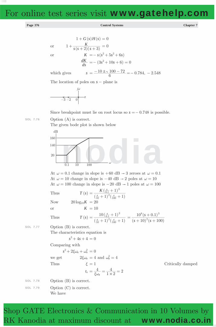
Page 376 Control Systems Chapter 7
nodia
Shop GATE Electronics & Communication in 10 Volumes by RK Kanodia at maximum discount at www.nodia.co.in
For online test series visit www.gatehelp.com
( ) ( )G s H s1 + 0=
or ( )( )s s s
K12 3
++ +
0=
or K ( )s s s s5 62 2=- + +
dsdK ( )s s3 10 6 02=- + + =
which gives s 0.784, 2.5486
10 100 72!= - - =- -
The location of poles on s - plane is
Since breakpoint must lie on root locus so .s 0 748=- is possible.
SOL 7.76 Option (A) is correct.The given bode plot is shown below
At .0 1w = change in slope is 60+ dB 3" zeroes at .0 1w =At 10w = change in slope is 40- dB 2" poles at 10w =At 100w = change in slope is 20- dB 1" poles at 100w =
Thus ( )T s ( ) ( )
( )K1 1
1.s s
s
102
100
0 13
=+ +
+
Now log K20 10 20=or K 10=
Thus ( )T s ( ) ( )
( )1 1
10 1.s s
s
102
100
0 13
=+ +
+
( ) ( )( . )
s ss
10 10010 0 1
2
8 3
=+ +
+
SOL 7.77 Option (B) is correct.The characteristics equation is
s s4 42 + + 0=Comparing with
s 2 n n2 2xw w+ + 0=
we get 2 nxw 4= and 4n2w =
Thus x 1= Critically damped
ts 41 2
4 2n #xw
= = =
SOL 7.78 Option (B) is correct.
SOL 7.79 Option (C) is correct.We have

Chapter 7 Control Systems Page 377
nodia
Shop GATE Electronics & Communication in 10 Volumes by RK Kanodia at maximum discount at www.nodia.co.in
For online test series visit www.gatehelp.com
xx1
2o
o= G
xx
11
01
1
2= = =G G and
( )( )
xx
00
10
1
2== =G G
A 11
01= = G
( )sI A- s
ss
s00 1
101
11
01= - =
-- -= = =G G G
( )sI A 1- - ( )
( )( )s
ss1
1 11
01
0
( )
s
s s2
11
11
11
2
=-
-+ - = -
-+
-> >H H
[( ) ]L sI A1 1-- - eete e
0Att
t t= = = G
( )x t [ ( )]e x tete e
ete
0 10
Att
t t
t
t0#= = == = =G G G
SOL 7.80 Option (C) is correct.The characteristics equation is
ks s 62 + + 0=
or sK
sK
1 62 + + 0=
Comparing with s s2 n n2 2xw w+ + 0= we have
we get 2 nxw K1= and
K6
n2w =
or . K2 0 5 6# # w K1
= Given .0 5x =
or K6
K1
2= & K 61=
SOL 7.81 Option (B) is correct.Any point on real axis lies on the root locus if total number of poles and zeros to the right of that point is odd. Here .s 1 5=- does not lie on real axis because there are total two poles and zeros (0 and 1- ) to the right of .s 1 5=- .
SOL 7.82 Option (D) is correct.From the expression of OLTF it may be easily see that the maximum magnitude is 0.5 and does not become 1 at any frequency. Thus gain cross over frequency does not exist. When gain cross over frequency does not exist, the phase margin is infinite.
SOL 7.83 Option (D) is correct.
We have ( )x to ( ) ( )x t u t2 2=- + ...(i)
Taking Laplace transform we get
( )sX s ( ) ( )X s U s2 2=- +or ( ) ( )s X s2+ ( )U s2=
or ( )X s ( )
( )sU s
22=+
Now ( )y t . ( )x t0 5= ( )Y s . ( )X s0 5=
or ( )Y s . ( )
sU s2
0 5 2#=+
or ( )( )
U sY s
( )s 2
1=+

Page 378 Control Systems Chapter 7
nodia
Shop GATE Electronics & Communication in 10 Volumes by RK Kanodia at maximum discount at www.nodia.co.in
For online test series visit www.gatehelp.com
SOL 7.84 Option (D) is correct.From Mason gain formula we can write transfer function as
( )( )
R sY s
( ) ( )s K
K1 3 3s s
KsK
3=- +
= - --
For system to be stable ( )K3 0<- i.e. K 3>
SOL 7.85 Option (B) is correct.The characteristics equation is
( )( )s s1 100+ + 0= s s101 1002 + + 0=Comparing with s 2 n n
2 2xw w+ + 0= we get
2 nxw 101= and 100n2w =
Thus x 20101= Overdamped
For overdamped system settling time can be determined by the dominant pole
of the closed loop system. In given system dominant pole consideration is at
s 1=- . Thus
T1 1= and Ts sec
T4 4= =
SOL 7.86 Option (B) is correct.Routh table is shown below. Here all element in 3rd row are zero, so system is marginal stable.
s5 2 4 2
s4 1 2 1
s3 0 0 0
s2
s1
s0
SOL 7.87 Option (B) is correct.The open loop transfer function is
( ) ( )G s H s ( )s s s 1
12=+ +
Substituting s jw= we have
( ) ( )G j H jw w ( )j j 1
12w w w
=- + +
( ) ( )G j H j+ w w ( )
tan2 11
2p
ww=- --
-
The frequency at which phase becomes 180c- , is called phase crossover
frequency.
Thus 180- 90 tan1
12w
w=- -- f
f-
or 90- tan1
12w
w=-- f
f-
or 1 2w- f 0=

Chapter 7 Control Systems Page 379
nodia
Shop GATE Electronics & Communication in 10 Volumes by RK Kanodia at maximum discount at www.nodia.co.in
For online test series visit www.gatehelp.com
wf 1= rad/sec
The gain margin at this frequency 1w =f is
GM ( ) ( )log G j H j20 10 w w=- f f
( ( )log20 1102 2 2w w w= - +f f f log20 1 0=- =
SOL 7.88 Option (A) is correct.
Z P N= -N " Net encirclement of ( )j1 0- + by Nyquist plot,
P " Number of open loop poles in right had side of s - plane
Z " Number of closed loop poles in right hand side of s - plane
Here N 0= (1 encirclement in CW direction and other in CCW)
and P 0=Thus Z 0=Hence there are no roots on RH of s - plane.
SOL 7.89 Option (D) is correct.Take off point is moved after G2 as shown below
SOL 7.90 Option (D) is correct.If roots of characteristics equation lie on negative axis at different positions (i.e. unequal), then system response is over damped.From the root locus diagram we see that for K0 1< < , the roots are on imaginary axis and for K1 5< < roots are on complex plain. For K 5> roots are again on imaginary axis.Thus system is over damped for 0 1K <# and K 5> .
SOL 7.91 Option (C) is correct.
The characteristics equation is
s s2 22 + + 0=Comparing with s 2 n n
2 2xw w+ + 0= we get
2 nxw 2= and 2n2w =
nw 2=
and x 2
1=
Since 1<x thus system is under damped
SOL 7.92 Option (C) is correct.From SFG we have
( )I s1 ( ) ( )G V s HI si1 2= + ...(1)
( )I s2 ( )G I s2 1= ...(2)
( )V s0 ( )G I s3 2= ...(3)
Now applying KVL in given block diagram we have
( )V si ( ) ( ) [ ( ) ( )] ( )I s Z s I s I s Z s1 1 1 2 3= + - ...(4)

Page 380 Control Systems Chapter 7
nodia
Shop GATE Electronics & Communication in 10 Volumes by RK Kanodia at maximum discount at www.nodia.co.in
For online test series visit www.gatehelp.com
0 [ ( ) ( )] ( ) ( ) ( ) ( ) ( )I s I s Z s I s Z s I s Z s2 1 3 2 2 2 4= - + + ...(5)
From (4) we have
or ( )V si ( )[ ( ) ( )] ( ) ( )I s Z s Z S I s Z S1 1 3 2 3= + -
or ( )I s1 ( ) ( ) ( ) ( )
( )V
Z s Z sI
Z s Z sZ s1
i1 3
21 3
3=+
++
...(6)
From (5) we have
( ) ( )I s Z S1 3 ( )[ ( ) ( ) ( )]I s Z s Z s Z s2 2 3 4= + + ...(7)
or ( )I ss ( ) ( ) ( )
( ) ( )Z s Z s Z s
I s Z s3 2 4
1 3=+ +
Comparing (2) and (7) we have
G2 ( ) ( ) ( )( )
Z s Z s Z sZ s
3 2 4
3=+ +
Comparing (1) and (6) we have
H ( ) ( )
( )Z s Z s
Z s1 3
3=+
SOL 7.93 Option (B) is correct.For unity negative feedback system the closed loop transfer function is
CLTF ( )
( )G s
G ss s
s1 7 13
42=
+=
+ ++ , ( )G s OL" Gain
or ( )
( )G s
G s1 +
ss s
47 132
=+
+ +
or ( )G s1
ss s
47 13 1
2=
++ + -
ss s
46 92
=+
+ +
or ( )G s s s
s6 9
42=+ ++
For DC gain s 0= , thus
Thus ( )G 0 94=
SOL 7.94 Option (C) is correct.From the Block diagram transfer function is
( )T s ( ) ( )( )
G s H sG s
1=
+
Where ( )G s ( )( )s
K s22=
+-
and ( )H s ( )s 2= -The Characteristic equation is
( ) ( )G s H s1 + 0=
( )
( )( )
sK s
s12
222+
+- - 0=
or ( ) ( )s K s2 22 2+ + - 0=or ( ) ( )K s K s K1 4 1 4 42+ + - + + 0=Routh Table is shown below. For System to be stable k1 0>+ , and k4 4 0>+
and k4 4 0>- . This gives K1 1< <-As per question for K0 1<#

Chapter 7 Control Systems Page 381
nodia
Shop GATE Electronics & Communication in 10 Volumes by RK Kanodia at maximum discount at www.nodia.co.in
For online test series visit www.gatehelp.com
s2 k1 + k4 4+
s1 k4 4- 0
s0 k4 4+
SOL 7.95 Option (B) is correct.It is stable at all frequencies because for resistive network feedback factor is always less than unity. Hence overall gain decreases.
SOL 7.96 Option (B) is correct.The characteristics equation is s s ks 32 2a+ + + 0=The Routh Table is shown below
For system to be stable 0>a and K 3 0>a
a -
Thus 0>a and K 3>a
s3 1 K
s2 a 3
s1 K 3a
a - 0
s0 3
SOL 7.97 Option (B) is correct.Closed loop transfer function is given as
( )T s s s4 9
92=+ +
by comparing with standard form we get natural freq.
A2w 9=
nw 3= 2 nxw 4=
Damping factor x /2 34 2 3#
= =
For second order system the setting time for 2-percent band is given by
ts 4
nxw= /3 2 3
424
#= = 2=
SOL 7.98 Option (D) is correct.Given loop transfer function is
( ) ( )G s H s ( )s s 1
2= +
( ) ( )G j H jw w ( )j j 1
2w w= +
Phase cross over frequency can be calculated as
( )at p
f ww w=
180c=-So here ( )f w ( )tan90 1c w=- - -
( )tan90 p1c w- - - 180c=-
( )tan p1 w- 90c=
pw 3=

Page 382 Control Systems Chapter 7
nodia
Shop GATE Electronics & Communication in 10 Volumes by RK Kanodia at maximum discount at www.nodia.co.in
For online test series visit www.gatehelp.com
Gain margin
20( ) ( )
log atG j H j
110 w w w= G pw=
. .G M ( ) ( )
logG j H j
20 1p
10 w w= e o
( ) ( )G j H jp pw w 1
2 0p p
2w w=
+=
so . .G M log20 01
10 3= =b l
SOL 7.99 Option (A) is correct.
Here A 02
13= -= G, B
01= = G and C [ ]1 1=
The controllability matrix is
QC [ ]B AB= 01
13= -= G
detQC 0! Thus controllable
The observability matrix is
Q0 [ ]C A CT T T= 011
22 != -= G
detQ0 0! Thus observable
SOL 7.100 Option (D) is correct.
we have ( ) ( )G s H s ( )s s 12 3= +
or ( ) ( )G j H jw w ( )j j 12 3
w w= +Gain cross over frequency
( ) ( )G j H jat g
w ww w=
1=
or 1
2 32w w +
1=
12 ( )12 2w w= + 124 2w w+ - 0= ( 4)( )32 2w w+ - 0= 2w 3= and 42w =-
which gives ,1 2w w 3!=
gw 3= ( )
at g
f ww w=
90 ( )tan g1 w=- - -
tan90 31=- - -
90 60=- - 150=- Phase margin ( )180
at g
f w= +w w=
180 150= - 30c=
SOL 7.101 Option (B) is correct.
SOL 7.102 Option (C) is correct.Closed-loop transfer function is given by
( )T s ...s a s a s a
a s an n
n n
n n
11
1
1=+ + + +
+-
-
-

Chapter 7 Control Systems Page 383
nodia
Shop GATE Electronics & Communication in 10 Volumes by RK Kanodia at maximum discount at www.nodia.co.in
For online test series visit www.gatehelp.com
1
...
...
s a s a sa s a
s a s a sa s a
n nn
n n
n nn
n n
11
22
1
11
22
1
=+
+ ++
+ ++
--
-
--
-
Thus ( ) ( )G s H s ....s a s a s
a s an n
n
n n
11
22
1=+ +
+-
-
-
For unity feed back ( )H s 1=
Thus ( )G s ....s a s a s
a s an n
n
n n
11
22
1=+ +
+-
-
-
Steady state error is given by
( )E s ( )( ) ( )
limR sG s H s1
1s 0
= +"
for unity feed back ( )H s 1=
Here input ( )R s ( )unit Ramps12=
so ( )E s ( )
lims G s1
11
s 0 2= +"
....
....lims s a s a
s a s a s1s n n
n
n nn
0 21
11
12
2
=+ + +
+ + +" -
--
aa
n
n 2= -
SOL 7.103 Option (B) is correct.
SOL 7.104 Option (A) is correct.
SOL 7.105 Option (A) is correct.Applying Routh’s criteria
s s s5 7 33 2+ + + 0=
s3 1 7
s2 5 3
s15
7 5 3532=# - 0
s0 3
There is no sign change in the first column. Thus there is no root lying in the left-half plane.
SOL 7.106 Option (A) is correct.Techometer acts like a differentiator so its transfer function is of the form ks .
SOL 7.107 Option (A) is correct.Open loop transfer function is
( )G s ( )s s
K1
= +Steady state error
( )E s ( ) ( )( )
limG s H ssR s
1s 0= +"
Where ( )R s ( )input H s 1= = (unity feedback)
( )R s s1=
Page 384 Control Systems Chapter 7
nodia
Shop GATE Electronics & Communication in 10 Volumes by RK Kanodia at maximum discount at www.nodia.co.in
For online test series visit www.gatehelp.com
so ( )E s
( )
( )lim lim
s sK
sss s Ks s
11
11
0s s0 0 2=
+ +
=+ +
+ =" "
SOL 7.108 Option (B) is correct.Fig given below shows a unit impulse input given to a zero-order hold circuit which holds the input signal for a duration T & therefore, the output is a unit step function till duration T .
( )h t ( ) ( )u t u t T= - -Taking Laplace transform we have
( )H s s s e1 1 sT= - - s e1 1 sT= - -6 @
SOL 7.109 Option (C) is correct.
Phase margin 180 gc q= + where gq value= of phase at gain crossover
frequency.
Here gq 125c=-so P.M 180 125 55c c c= - =
SOL 7.110 Option (B) is correct.Open loop transfer function is given by
( ) ( )G s H s ( )( )
( . )s s s
K s1 1 2
1 0 5= + ++
Close looped system is of type 1.
It must be noted that type of the system is defined as no. of poles lyinglies at origin
in OLTF.
SOL 7.111 Option (D) is correct.Transfer function of the phase lead controller is
.T F ( )( )
sTs
T jT j
11 3
11 3
ww= +
+ = ++
Phase is
( )f w ( ) ( )tan tanT T31 1w w= -- -
( )f w tanT
T T1 331
2 2ww w=
+--
; E
( )f w tanT
T1 3
212 2w
w=+
-; E
For maximum value of phase
( )
dd
wf w
0=
or 1 T3 2 2w=
Tw 3
1=
Chapter 7 Control Systems Page 385
nodia
Shop GATE Electronics & Communication in 10 Volumes by RK Kanodia at maximum discount at www.nodia.co.in
For online test series visit www.gatehelp.com
So maximum phase is
maxf tanT
T1 3
212 2w
w=+
-; E at T
31w =
30tan tan1 3
2
311
31
31
1
#c=
+= =- -
> ;H E
SOL 7.112 Option (A) is correct.( ) ( )G j H jw w enclose the ( 1, 0)- point so here ( ) ( )G j H j 1>p pw w
pw Phase= cross over frequency
Gain Margin ( ) ( )
logG j H j
20 1p p
10 w w=
so gain margin will be less than zero.
SOL 7.113 Option (B) is correct.The denominator of Transfer function is called the characteristic equation of the system. so here characteristic equation is
( 1) ( 2)s s 02+ + =
SOL 7.114 Option (C) is correct.In synchro error detector, output voltage is proportional to [ ( )]tw , where ( )tw is the rotor velocity so here n 1=
SOL 7.115 Option (C) is correct.By masson’s gain formulae
xy
Pk k
DD= /
Forward path gain P1 5 2 1 10# #= = D ( )1 2 2 1 4 5#= - - = + = 1D 1=
so gain xy 5
10 1 2#= =
SOL 7.116 Option (C) is correct.By given matrix equations we can have
X1o dt
dx x x 011 2= = - +
X2o dt
dx x022 m= = + +
y [ ]xx x x1 1
1
21 2= = +> H
dtdy dt
dxdtdx1 2= +
dtdy x1 m= +
dtdy
t 0= ( ) ( )x 0 01 m= +
1 0= + 0=
***********

CHAPTER 8ELECTROMAGNETICS
nodia
2013 ONE MARK
MCQ 8.1 Consider a vector field A rv v^ h. The closed loop line integral A dl:v v# can be expressed as
(A) A ds# :d v v^ h## over the closed surface bounded by the loop
(B) A dv:d v^ h### over the closed volume bounded by the loop
(C) A dv:d v^ h### over the open volume bounded by the loop
(D) A ds# :d v v^ h## over the open surface bounded by the loop
MCQ 8.2 The divergence of the vector field A xa ya zax y z= + +v t t t is(A) 0 (B) 1/3
(C) 1 (D) 3
MCQ 8.3 The return loss of a device is found to be 20 dB. The voltage standing wave ratio (VSWR) and magnitude of reflection coefficient are respectively(A) 1.22 and 0.1 (B) 0.81 and 0.1
(C) – 1.22 and 0.1 (D) 2.44 and 0.2
2013 TWO MARKS
Statement for Linked Answer Questions 4 and 5:A monochromatic plane wave of wavelength 600 mml = is propagating in the direction as shown in the figure below. Ei
v , Erv and Et
v denote incident, reflected, and transmitted electric field vectors associated with the wave.
MCQ 8.4 The angle of incidence iq and the expression for Eiv are
(A) 60c and /V mE a a e2
x zj
x0
3 2
10 24
-#p
-+
t t^^
hh

Chapter 8 Electromagnetics Page 387
nodia
Shop GATE Electronics & Communication in 10 Volumes by RK Kanodia at maximum discount at www.nodia.co.in
For online test series visit www.gatehelp.com
(B) 45c and /V mE a a e2
x zj z
0 3104
+#p-t t^ h
(C) 45c and /V mE a a e2
x zj
x z0
3 2
104
-#p
-+
t t^^
hh
(D) 60c and /V mE a a e2
x zj z
0 3104
-#p-t t^ h
MCQ 8.5 The expression for Erv is
(A) 0.23 /V mE a a e2
x zj
x z0
3 2
104
+#p
--
t t^^
hh
(B) /V mE a a e2
x zj z
0 3104
- +#p
t t^ h
(C) 0.44 /V mE a a e2
x zj
x z0
3 2
104
+#p
--
t t^^
hh
(D) /V mE a a e2
x zj
x z0 3
104
+#p
-+
t t^^
hh
2012 ONE MARK
MCQ 8.6 A plane wave propagating in air with (8 6 5 ) /V meE a a a ( )x y z
j t x y3 4= + + w + - is incident on a perfectly conducting slab positioned at x 0# . The E field of the reflected wave is(A) ( 8 6 5 ) /V mea a a ( )
x y zj t x y3 4- - - w + +
(B) ( 8 6 5 ) /V mea a a ( )x y z
j t x y3 4- + - w + + -
(C) ( 8 6 5 ) /V mea a a ( )x y z
j t x y3 4- - - w - -
(D) ( 8 6 5 ) /V mea a a ( )x y z
j t x y3 4- + - w - -
MCQ 8.7 The electric field of a uniform plane electromagnetic wave in free space, along the positive x direction is given by 10( )j eE a ay z
j x25= + - . The frequency and polarization of the wave, respectively, are(A) 1.2 GHz and left circular (B) 4 Hz and left circular
(C) 1.2 GHz and right circular (D) 4 Hz and right circular
MCQ 8.8 A coaxial-cable with an inner diameter of mm1 and outer diameter of 2.4 mm is filled with a dielectric of relative permittivity 10.89. Given 4 10 / ,H m0
7m p#= -
/F m3610
0
9
e p=-
, the characteristic impedance of the cable is
(A) 330W (B) 100W(C) 143.3W (D) 43.4 W
MCQ 8.9 The radiation pattern of an antenna in spherical co-ordinates is given by ( )F q ; /cos 0 24 # #q q p= . The directivity of the antenna is
(A) 10 dB (B) 12.6 dB
(C) 11.5 dB (D) 18 dB
2012 TWO MARKS
MCQ 8.10 A transmission line with a characteristic impedance of 100W is used to match a 50W section to a 200W section. If the matching is to be done both at 429 MHz and 1GHz, the length of the transmission line can be approximately

Page 388 Electromagnetics Chapter 8
nodia
Shop GATE Electronics & Communication in 10 Volumes by RK Kanodia at maximum discount at www.nodia.co.in
For online test series visit www.gatehelp.com
(A) 82.5 cm (b) 1.05 m
(C) 1.58 cm (D) 1.75 m
MCQ 8.11 The magnetic field among the propagation direction inside a rectangular waveguide with the cross-section shown in the figure is
Hz ( . ) ( . ) ( . )cos cos cosx y t z3 2 094 10 2 618 10 6 283 102 2 10# # # b= -
The phase velocity vp of the wave inside the waveguide satisfies(A) v c>p (B) v cp =(C) v c0 < <p (D) v 0p =
Statement for Linked Answer Question 12 and 13 :An infinitely long uniform solid wire of radius a carries a uniform dc current of density J
MCQ 8.12 The magnetic field at a distance r from the center of the wire is proportional to(A) 1/for and forr r a r r a< >2 (B) 1/for and forr a r r a0 < >(C) 1/for and forr r a r r a< > (D) 0 1/for and forr a r r a< >2
MCQ 8.13 A hole of radius ( )b b a< is now drilled along the length of the wire at a distance d from the center of the wire as shown below.
The magnetic field inside the hole is(A) uniform and depends only on d
(B) uniform and depends only on b
(C) uniform and depends on both andb d
(D) non uniform
2011 ONE MARK
MCQ 8.14 Consider the following statements regarding the complex Poynting vector Pv for the power radiated by a point source in an infinite homogeneous and lossless medium. Re(Pv) denotes the real part of ,P Sv denotes a spherical surface whose centre is at the point source, and nt denotes the unit surface normal on S . Which of the following statements is TRUE?

Chapter 8 Electromagnetics Page 389
nodia
Shop GATE Electronics & Communication in 10 Volumes by RK Kanodia at maximum discount at www.nodia.co.in
For online test series visit www.gatehelp.com
(A) Re(Pv) remains constant at any radial distance from the source
(B) Re(Pv) increases with increasing radial distance from the source
(C) ( )Re P n dSs
:v t## remains constant at any radial distance from the source
(D) ( )Re P n dSs
:v t## decreases with increasing radial distance from the source
MCQ 8.15 A transmission line of characteristic impedance 50W is terminated by a 50W load. When excited by a sinusoidal voltage source at 10 GHz, the phase difference between two points spaced 2 mm apart on the line is found to be /4p radians. The phase velocity of the wave along the line is(A) 0.8 10 /m s8
# (B) 1.2 10 /m s8#
(C) 1.6 10 /m s8# (D) 3 10 /m s8
#
MCQ 8.16 The modes in a rectangular waveguide are denoted by TMTE
mn
mn where m and n are the eigen numbers along the larger and smaller dimensions of the waveguide respectively. Which one of the following statements is TRUE?(A) The TM10 mode of the waveguide does not exist
(B) The TE10 mode of the waveguide does not exist
(C) The TM10 and the TE10 modes both exist and have the same cut-off frequencies
(D) The TM10 and the TM01 modes both exist and have the same cut-off frequencies
2011 TWO MARKS
MCQ 8.17 A current sheet 10 /A mJ uy=v t lies on the dielectric interface x 0= between two dielectric media with 5, 1r r1 1me = = in Region-1 ( )x 0< and 2, 2r r2 2me = = in Region-2 ( 0)x 2 . If the magnetic field in Region-1 at x 0= - is 3 30 /A mH u ux y1 = +v t t the magnetic field in Region-2 at x 0= + is
(A) 1.5 30 10 /A mH u u ux y z2 = + -v t t t
(B) 30 10 /A mH u u u3 x y z2 = + -v t t t
(C) 1.5 40 /A mH u ux y2 = +v t t
(D) 3 30 10 /A mH u u ux y z2 = + +v t t t
MCQ 8.18 A transmission line of characteristic impedance 50 W is terminated in a load impedance ZL . The VSWR of the line is measured as 5 and the first of the voltage maxima in the line is observed at a distance of l/4 from the load. The value of ZL is(A) 10 W (B) 250 W(C) (19.23 46.15)j W+ (D) (19.23 46.15)j W-
MCQ 8.19 The electric and magnetic fields for a TEM wave of frequency 14 GHz in a homogeneous medium of relative permittivity re and relative permeability 1rm =

Page 390 Electromagnetics Chapter 8
nodia
Shop GATE Electronics & Communication in 10 Volumes by RK Kanodia at maximum discount at www.nodia.co.in
For online test series visit www.gatehelp.com
are given by /V mE E e u( 280 )p
j t yz= pw -v t and 3 /A mH e u( 280 )j t y
x= pw -v t . Assuming the speed of light in free space to be 3 10 /m s8
# , the intrinsic impedance of free space to be 120p , the relative permittivity re of the medium and the electric field amplitude Ep are(A) 3, 120Er p pe = = (B) 3, 360Er p pe = =(C) 9, 360Er p pe = = (D) 9, 120Er p pe = =
2010 ONE MARK
MCQ 8.20 If the scattering matrix [ ]S of a two port network is
[ ]S .
0.9 900.9 900.1 90
0 2 0cc
c
c
++
++= > H, then the network is
(A) lossless and reciprocal (B) lossless but not reciprocal
(C) not lossless but reciprocal (D) neither lossless nor reciprocal
MCQ 8.21 A transmission line has a characteristic impedance of 50W and a resistance of 0.1 /mW . If the line is distortion less, the attenuation constant(in Np/m) is(A) 500 (B) 5
(C) 0.014 (D) 0.002
MCQ 8.22 The electric field component of a time harmonic plane EM wave traveling in a nonmagnetic lossless dielectric medium has an amplitude of 1 V/m. If the relative permittivity of the medium is 4, the magnitude of the time-average power density vector (in /W m2) is
(A) 301p (B) 60
1p
(C) 1201p (D) 240
1p
2010 TWO MARKS
MCQ 8.23 If A xya x ax y2= +v t t , then A dl
C$v v#o over the path shown in the figure is
(A) 0 (B) 3
2
(C) 1 (D) 2 3
MCQ 8.24 A plane wave having the electric field components 24cosE y a3 10i x8
# b= -v t^ h V/m and traveling in free space is incident normally on a lossless medium with
0m m= and 9 0e e= which occupies the region y 0$ . The reflected magnetic field component is given by
(A) 10 (3 10 ) /cos A mt y a1x
8
p # + t
Chapter 8 Electromagnetics Page 391
nodia
Shop GATE Electronics & Communication in 10 Volumes by RK Kanodia at maximum discount at www.nodia.co.in
For online test series visit www.gatehelp.com
(B) 20 (3 10 ) /cos A mt y a1x
8
p # + t
(C) 20 (3 10 ) /cos A mt y a1x
8
p #- + t
(D) 10 (3 10 ) /cos A mt y a1x
8
p #- + t
MCQ 8.25 In the circuit shown, all the transmission line sections are lossless. The Voltage Standing Wave Ration(VSWR) on the 60 W line is
(A) 1.00 (B) 1.64
(C) 2.50 (D) 3.00
2009 ONE MARK
MCQ 8.26 Two infinitely long wires carrying current are as shown in the figure below. One wire is in the y z- plane and parallel to the y - axis. The other wire is in the x y- plane and parallel to the x - axis. Which components of the resulting magnetic field are non-zero at the origin ?
(A) , ,x y z components (B) ,x y components
(C) ,y z components (D) ,x z components
MCQ 8.27 Which of the following statements is true regarding the fundamental mode of the metallic waveguides shown ?
(A) Only P has no cutoff-frequency
(B) Only Q has no cutoff-frequency
(C) Only R has no cutoff-frequency

Page 392 Electromagnetics Chapter 8
nodia
Shop GATE Electronics & Communication in 10 Volumes by RK Kanodia at maximum discount at www.nodia.co.in
For online test series visit www.gatehelp.com
(D) All three have cutoff-frequencies
2009 TWO MARKS
MCQ 8.28 If a vector field V is related to another vector field A through V A4#= , which of the following is true? (Note : C and SC refer to any closed contour and any surface whose boundary is C . )
(A) V Adl dSC CS
$ $= ### (B) A Vdl dSC CS
$ $= ###
(C) V Adl dSC CS
# $ $D D #= ### (D) V Vdl dSC CS
# $ $D = ###
MCQ 8.29 A transmission line terminates in two branches, each of length 4l , as shown.
The branches are terminated by 50W loads. The lines are lossless and have the characteristic impedances shown. Determine the impedance Zi as seen by the source.
(A) 200W (B) 100W(C) 50W (D) 25W
MCQ 8.30 A magnetic field in air is measured to be
B Bx y
x yx y
y x0 2 2 2 2=+
-+
t tc m
What current distribution leads to this field ?[Hint : The algebra is trivial in cylindrical coordinates.]
(A) , 0J B zx y
r10
02 2 !
m=
+tc m (B) , 0J B z
x yr2
0
02 2 !
m=-
+tc m
(C) 0, 0rJ != (D) , 0J B zx y
r10
02 2 !
m=
+tc m
2008 ONE MARK
MCQ 8.31 For a Hertz dipole antenna, the half power beam width (HPBW) in the E -plane is(A) 360c (B) 180c
(C) 90c (D) 45c
MCQ 8.32 For static electric and magnetic fields in an inhomogeneous source-free medium, which of the following represents the correct form of Maxwell’s equations ?(A) 0E4$ = , B 04# = (B) 0E4$ = , 0B4$ =(C) E 04# = , B 04# = (D) E 04# = , 0B4$ =
2008 TWO MARKS
MCQ 8.33 A rectangular waveguide of internal dimensions (a 4= cm and b 3= cm) is to be

Chapter 8 Electromagnetics Page 393
nodia
Shop GATE Electronics & Communication in 10 Volumes by RK Kanodia at maximum discount at www.nodia.co.in
For online test series visit www.gatehelp.com
operated in TE11 mode. The minimum operating frequency is(A) 6.25 GHz (B) 6.0 GHz
(C) 5.0 GHz (D) 3.75 GHz
MCQ 8.34 One end of a loss-less transmission line having the characteristic impedance of 75W and length of 1 cm is short-circuited. At 3 GHz, the input impedance at the other end of transmission line is(A) 0 (B) Resistive
(C) Capacitive (D) Inductive
MCQ 8.35 A uniform plane wave in the free space is normally incident on an infinitely thick dielectric slab (dielectric constant 9e = ). The magnitude of the reflection coefficient is(A) 0 (B) 0.3
(C) 0.5 (D) 0.8
MCQ 8.36 In the design of a single mode step index optical fibre close to upper cut-off, the single-mode operation is not preserved if(A) radius as well as operating wavelength are halved
(B) radius as well as operating wavelength are doubled
(C) radius is halved and operating wavelength is doubled
(D) radius is doubled and operating wavelength is halved
MCQ 8.37 At 20 GHz, the gain of a parabolic dish antenna of 1 meter and 70% efficiency is(A) 15 dB (B) 25 dB
(C) 35 dB (D) 45 dB
2007 ONE MARK
MCQ 8.38 A plane wave of wavelength l is traveling in a direction making an angle 30c with positive x - axis and 90c with positive y - axis. The E field of the plane wave can be represented as (E0 is constant)
(A) E yE ej t x z0
3= w l
plp- -t c m (B) E yE ej t x z
03
= w lp
lp- -t c m
(C) E yE ej t x z0
3= w l
plp+ +t c m (D) E yE ej t x z
03
= w lp
lp- +t c m
MCQ 8.39 If C is code curve enclosing a surface S , then magnetic field intensity H , the current density j and the electric flux density D are related by
(A) H Dds jt
dtS c
$ $22= +c m# # # #
(B) H Dd l jt
dSS S
$ $22= +c m# # #
(C) H DdS jt
dtS C
$ $22= +c m## #
(D) H Dd l jt
dsC S
c
$ $22= +c m# ## #
2007 TWO MARKS
MCQ 8.40 The E field in a rectangular waveguide of inner dimension a b# is given by

Page 394 Electromagnetics Chapter 8
nodia
Shop GATE Electronics & Communication in 10 Volumes by RK Kanodia at maximum discount at www.nodia.co.in
For online test series visit www.gatehelp.com
E ( )sin sinh
Ha
x t z y2
22 0
2wm l p w b= - t` `j j
Where H0 is a constant, and a and b are the dimensions along the x - axis and
the y - axis respectively. The mode of propagation in the waveguide is(A) TE20 (B) TM11
(C) TM20 (D) TE10
MCQ 8.41 A load of 50W is connected in shunt in a 2-wire transmission line of Z 500 W= as shown in the figure. The 2-port scattering parameter matrix (s-matrix) of the shunt element is
(A) 21
21
21
21
--> H (B)
01
10= G
(C) 31
32
32
31
--> H (D) 4
1
43
43
41-
-> H
MCQ 8.42 The parallel branches of a 2-wirw transmission line re terminated in 100W and 200W resistors as shown in the figure. The characteristic impedance of the line is
Z 500 W= and each section has a length of 4l . The voltage reflection coefficient G
at the input is
(A) j57- (B)
75-
(C) j75 (D)
75
MCQ 8.43 The H field (in A/m) of a plane wave propagating in free space is given by
( )H cosx t z y t z5 320h
w b w b p= - + - +t t` j.
The time average power flow density in Watts is
(A) 100
0h (B) 1000h
(C) 50 02h (D) 50
0h
MCQ 8.44 An air-filled rectangular waveguide has inner dimensions of 3 cm # 2 cm. The

Chapter 8 Electromagnetics Page 395
nodia
Shop GATE Electronics & Communication in 10 Volumes by RK Kanodia at maximum discount at www.nodia.co.in
For online test series visit www.gatehelp.com
wave impedance of the TE20 mode of propagation in the waveguide at a frequency of 30 GHz is (free space impedance 3770h W= )(A) 308 W (B) 355 W(C) 400 W (D) 461 W
MCQ 8.45 A 2l dipole is kept horizontally at a height of 2
0l above a perfectly conducting infinite ground plane. The radiation pattern in the lane of the dipole (E plane) looks approximately as
MCQ 8.46 A right circularly polarized (RCP) plane wave is incident at an angle 60c to the normal, on an air-dielectric interface. If the reflected wave is linearly polarized, the relative dielectric constant r2x is.
(A) 2 (B) 3
(C) 2 (D) 3
2006 ONE MARK
MCQ 8.47 The electric field of an electromagnetic wave propagation in the positive direction is given by ( ) ( /2)sin sinE a t z a t zx yw b w b p= - + - +t t . The wave is(A) Linearly polarized in the z -direction
(B) Elliptically polarized
(C) Left-hand circularly polarized
(D) Right-hand circularly polarized
MCQ 8.48 A transmission line is feeding 1 watt of power to a horn antenna having a gain of 10 dB. The antenna is matched to the transmission line. The total power radiated by the horn antenna into the free space is(A) 10 Watts (B) 1 Watts
(C) 0.1 Watts (D) 0.01 Watt
2006 TWO MARKS
MCQ 8.49 When a planes wave traveling in free-space is incident normally on a medium having the fraction of power transmitted into the medium is given by

Page 396 Electromagnetics Chapter 8
nodia
Shop GATE Electronics & Communication in 10 Volumes by RK Kanodia at maximum discount at www.nodia.co.in
For online test series visit www.gatehelp.com
(A) 98 (B)
21
(C) 31 (D)
65
MCQ 8.50 A medium of relative permittivity 2r2e = forms an interface with free - space. A point source of electromagnetic energy is located in the medium at a depth of 1 meter from the interface. Due to the total internal reflection, the transmitted beam has a circular cross-section over the interface. The area of the beam cross-section at the interface is given by(A) 2p m2 (B) 2p m2
(C) 2p m2 (D) p m2
MCQ 8.51 A rectangular wave guide having TE10 mode as dominant mode is having a cut off frequency 18 GHz for the mode TE30. The inner broad - wall dimension of the rectangular wave guide is(A) 5/3 cm (B) 5 cm
(C) 5/2 cm (D) 10 cm
MCQ 8.52 A medium is divide into regions I and II about x 0= plane, as shown in the figure below.
An electromagnetic wave with electric field 4 3 5E a a ax y z1 = + +t t t is incident normally on the interface from region I . The electric file E2 in region II at the interface is(A) E E2 1= (B) 4 0.75 1.25a a ax y z+ -t t t
(C) 3 3 5a a ax y z+ +t t t (D) 3 3 5a a ax y z- + +t t t
MCQ 8.53 A mast antenna consisting of a 50 meter long vertical conductor operates over a perfectly conducting ground plane. It is base-fed at a frequency of 600 kHz. The radiation resistance of the antenna is Ohms is
(A) 5
2 2p (B) 5
2p
(C) 5
4 2p (D) 20 2p
2005 ONE MARK
MCQ 8.54 The magnetic field intensity vector of a plane wave is given by
( , , , )H x y z t 10 (50000 0.004 30)sin t x ay= + + t
where ayt , denotes the unit vector in y direction. The wave is propagating with a
phase velocity.(A) 5 104# m/s (B) 3 108#- m/s
(C) .1 25 107#- m/s (D) 3 108# m/s

Chapter 8 Electromagnetics Page 397
nodia
Shop GATE Electronics & Communication in 10 Volumes by RK Kanodia at maximum discount at www.nodia.co.in
For online test series visit www.gatehelp.com
MCQ 8.55 Refractive index of glass is 1.5. Find the wavelength of a beam of light with frequency of 1014 Hz in glass. Assume velocity of light is 3 108# m/s in vacuum(A) 3 mm (B) 3 mm
(C) 2 mm (D) 1 mm
2005 TWO MARKS
MCQ 8.56 Which one of the following does represent the electric field lines for the mode in the cross-section of a hollow rectangular metallic waveguide ?
MCQ 8.57 Characteristic impedance of a transmission line is 50 W. Input impedance of the open-circuited line when the transmission line a short circuited, then value of the input impedance will be.(A) 50 W (B) j100 150W+(C) . .j7 69 11 54W+ (D) . .j7 69 11 54W-
MCQ 8.58 Two identical and parallel dipole antennas are kept apart by a distance of 4l in
the H - plane. They are fed with equal currents but the right most antenna has a phase shift of 90c+ . The radiation pattern is given as.
Statement of Linked Answer Questions 59 & 60 :Voltage standing wave pattern in a lossless transmission line with characteristic impedance 50 and a resistive load is shown in the figure.

Page 398 Electromagnetics Chapter 8
nodia
Shop GATE Electronics & Communication in 10 Volumes by RK Kanodia at maximum discount at www.nodia.co.in
For online test series visit www.gatehelp.com
MCQ 8.59 The value of the load resistance is(A) 50 W (B) 200 W(C) 12.5 W (D) 0
MCQ 8.60 The reflection coefficient is given by(A) .0 6- (B) 1-(C) 0.6 (D) 0
MCQ 8.61 Many circles are drawn in a Smith Chart used for transmission line calculations. The circles shown in the figure represent
(A) Unit circles
(B) Constant resistance circles
(C) Constant reactance circles
(D) Constant reflection coefficient circles.
2004 ONE MARK
MCQ 8.62 The phase velocity of an electromagnetic wave propagating in a hollow metallic rectangular waveguide in the TE10 mode is(A) equal to its group velocity
(B) less than the velocity of light in free space
(C) equal to the velocity of light in free space
(D) greater than the velocity of light in free space
MCQ 8.63 Consider a lossless antenna with a directive gain of 6+ dB. If 1 mW of power is fed to it the total power radiated by the antenna will be(A) 4 mW (B) 1 mW
(C) 7 mW (D) 1/4 mW
2004 TWO MARKS
MCQ 8.64 A parallel plate air-filled capacitor has plate area of 10 4- m2 and plate separation of 10 3- m. It is connect - ed to a 0.5 V, 3.6 GHz source. The magnitude of the displacement current is ( 1036
1 9e = p- F/m)
(A) 10 mA (B) 100 mA
(C) 10 A (D) 1.59 mA
MCQ 8.65 Consider a 300 W, quarter - wave long (at 1 GHz) transmission line as shown in Fig. It is connected to a 10 V, 50 W source at one end and is left open circuited at the other end. The magnitude of the voltage at the open circuit end of the line is

Chapter 8 Electromagnetics Page 399
nodia
Shop GATE Electronics & Communication in 10 Volumes by RK Kanodia at maximum discount at www.nodia.co.in
For online test series visit www.gatehelp.com
(A) 10 V (B) 5 V
(C) 60 V (D) 60/7 V
MCQ 8.66 In a microwave test bench, why is the microwave signal amplitude modulated at 1 kHz(A) To increase the sensitivity of measurement
(B) To transmit the signal to a far-off place
(C) To study amplitude modulations
(D) Because crystal detector fails at microwave frequencies
MCQ 8.67 If ( )E a ja ex yjkz k t= + w-t t and ( / )( )H k a ka ey x
jkz j twm= + w-t t , the time-averaged Poynting vector is(A) null vector (B) ( / )k azwm t
(C) (2 / )k azwm t (D) ( /2 )k azwm t
MCQ 8.68 Consider an impedance Z R jX= + marked with point P in an impedance Smith chart as shown in Fig. The movement from point P along a constant resistance circle in the clockwise direction by an angle 45c is equivalent to
(A) adding an inductance in series with Z
(B) adding a capacitance in series with Z
(C) adding an inductance in shunt across Z
(D) adding a capacitance in shunt across Z
MCQ 8.69 A plane electromagnetic wave propagating in free space is incident normally on a large slab of loss-less, non-magnetic, dielectric material with > 0e e . Maxima and minima are observed when the electric field is measured in front of the slab. The maximum electric field is found to be 5 times the minimum field. The intrinsic impedance of the medium should be(A) 120p W (B) 60p W(C) 600p W (D) 24p W
MCQ 8.70 A lossless transmission line is terminated in a load which reflects a part of the incident power. The measured VSWR is 2. The percentage of the power that is reflected back is(A) 57.73 (B) 33.33
(C) 0.11 (D) 11.11

Page 400 Electromagnetics Chapter 8
nodia
Shop GATE Electronics & Communication in 10 Volumes by RK Kanodia at maximum discount at www.nodia.co.in
For online test series visit www.gatehelp.com
2003 ONE MARK
MCQ 8.71 The unit of H4# is(A) Ampere (B) Ampere/meter
(C) Ampere/meter2 (D) Ampere-meter
MCQ 8.72 The depth of penetration of electromagnetic wave in a medium having conductivity s at a frequency of 1 MHz is 25 cm. The depth of penetration at a frequency of 4 MHz will be(A) 6.25 dm (B) 12.50 cm
(C) 50.00 cm (D) 100.00 cm
2003 TWO MARKS
MCQ 8.73 Medium 1 has the electrical permittivity .1 51 0e e= farad/m and occupies the region to the left of x 0= plane. Medium 2 has the electrical permittivity .2 52 0e e= farad/m and occupies the region to the right of x 0= plane. If E1 in medium 1 is
(2 3 1 )E u u ux y z1 = - + volt/m, then E2 in medium 2 is(A) (2.0 7.5 2.5 )u u ux y z- + volt/m
(B) (2.0 2.0 0.6 )u u ux y z- + volt/m
(C) (2.0 3.0 1.0 )u u ux y z- + volt/m
(D) (2.0 2.0 0.6 )u u ux y z- + volt/m
MCQ 8.74 If the electric field intensity is given by ( )E xu yu zux y z= + + volt/m, the potential difference between ( , , )X 2 0 0 and ( , , )Y 1 2 3 is(A) 1+ volt (B) 1- volt
(C) 5+ volt (D) 6+ volt
MCQ 8.75 A uniform plane wave traveling in air is incident on the plane boundary between air and another dielectric medium with 4re = . The reflection coefficient for the normal incidence, is(A) zero (B) .0 5 180c+
(B) .0 333 0c+ (D) .0 333 180c+
MCQ 8.76 If the electric field intensity associated with a uniform plane electromagnetic wave traveling in a perfect dielectric medium is given by ( , )E z t ( . )cos t z10 2 10 0 17p p= - V/m, then the velocity of the traveling wave is(A) .3 00 108# m/sec (B) .2 00 108# m/sec
(C) .6 28 107# m/sec (D) .2 00 107# m/sec
MCQ 8.77 Two identical antennas are placed in the /2q p= plane as shown in Fig. The elements have equal amplitude excitation with 180c polarity difference, operating at wavelength l. The correct value of the magnitude of the far-zone resultant electric field strength normalized with that of a single element, both computed for 0f = , is

Chapter 8 Electromagnetics Page 401
nodia
Shop GATE Electronics & Communication in 10 Volumes by RK Kanodia at maximum discount at www.nodia.co.in
For online test series visit www.gatehelp.com
(A) 2 cos s2lp
b l (B) 2 sin s2lp
b l
(C) 2 cos slp
a k (D) 2 sin slp
a k
MCQ 8.78 A short - circuited stub is shunt connected to a transmission line as shown in fig. If Z 500 = ohm, the admittance Y seen at the junction of the stub and the transmission line is
(A) ( . . )j0 01 0 02- mho (B) ( . . )j0 02 0 01- mho
(C) ( . . )j0 04 0 02- mho (D) ( . )j0 02 0+ mho
MCQ 8.79 A rectangular metal wave guide filled with a dielectric material of relative permittivity 4re = has the inside dimensions 3.0 cm # 1.2 cm. The cut-off frequency for the dominant mode is(A) 2.5 GHz (B) 5.0 GHz
(C) 10.0 GHz (D) 12.5 GHz
2002 ONE MARK
MCQ 8.80 The VSWR can have any value between(A) 0 and 1 (B) 1- and 1+(C) 0 and 3 (D) 1 and 3
MCQ 8.81 In in impedance Smith movement along a constant resistance circle gives rise to(A) a decrease in the value of reactance
(B) an increase in the value of reactance
(C) no change in the reactance value
(D) no change in the impedance
MCQ 8.82 The phase velocity for the TE10 -mode in an air-filled rectangular waveguide is (c is the velocity of plane waves in free space)(A) less than c (B) equal to c
(C) greater than c (D) none of these
2002 TWO MARKS
MCQ 8.83 A plane wave is characterized by (0.5 )E x ye e/j j t jkz2= + p w -t t . This wave is

Page 402 Electromagnetics Chapter 8
nodia
Shop GATE Electronics & Communication in 10 Volumes by RK Kanodia at maximum discount at www.nodia.co.in
For online test series visit www.gatehelp.com
(A) linearly polarized (B) circularly polarized
(C) elliptically polarized (D) unpolarized
MCQ 8.84 Distilled water at 25c C is characterized by .1 7 10 4#s = - mho/m and 78 oe e= at a frequency of 3 GHz. Its loss tangent tan d is ( 36
10 9
e = p-
F/m)
(A) .1 3 10 5#
- (B) 1.3 10 3#
-
(C) 1.3 10 /784#
- (D) 1.3 10 /7850e#
-
MCQ 8.85 The electric field on the surface of a perfect conductor is 2 V/m. The conductor is immersed in water with 80 oe e= . The surface charge density on the conductor is ( 36
10 9
e = p-
F/m)(A) 0 C/m2 (B) 2 C/m2
(C) .1 8 10 11#- C/m2 (D) .1 41 10 9#
- C/m2
MCQ 8.86 A person with receiver is 5 Km away from the transmitter. What is the distance that this person must move further to detect a 3-dB decrease in signal strength(A) 942 m (B) 2070 m
(C) 4978 m (D) 5320 m
2001 ONE MARK
MCQ 8.87 A transmission line is distortonless if
(A) RLGC1= (B) RL GC=
(C) LG RC= (D) RG LC=
MCQ 8.88 If a plane electromagnetic wave satisfies the equal ZE c
tEx x
2
22
2
2
dd
dd= , the wave
propagates in the(A) x - direction
(B) z - direction
(C) y - direction
(D) xy plane at an angle of 45c between the x and z direction
MCQ 8.89 The plane velocity of wave propagating in a hollow metal waveguide is(A) grater than the velocity of light in free space
(B) less than the velocity of light in free space
(C) equal to the velocity of light free space
(D) equal to the velocity of light in free
MCQ 8.90 The dominant mode in a rectangular waveguide is TE10, because this mode has(A) the highest cut-off wavelength
(B) no cut-off
(C) no magnetic field component
(D) no attenuation

Chapter 8 Electromagnetics Page 403
nodia
Shop GATE Electronics & Communication in 10 Volumes by RK Kanodia at maximum discount at www.nodia.co.in
For online test series visit www.gatehelp.com
2001 TWO MARKS
MCQ 8.91 A material has conductivity of 10 2- mho/m and a relative permittivity of 4. The frequency at which the conduction current in the medium is equal to the displacement current is(A) 45 MHz (B) 90 MHz
(C) 450 MHz (D) 900 MHz
MCQ 8.92 A uniform plane electromagnetic wave incident on a plane surface of a dielectric material is reflected with a VSWR of 3. What is the percentage of incident power that is reflected ?(A) 10% (B) 25%
(C) 50% (D) 75%
MCQ 8.93 A medium wave radio transmitter operating at a wavelength of 492 m has a tower antenna of height 124. What is the radiation resistance of the antenna?(A) 25 W (B) 36.5 W(C) 50 W (D) 73 W
MCQ 8.94 In uniform linear array, four isotropic radiating elements are spaced 4l apart. The
progressive phase shift between required for forming the main beam at 60c off the end - fire is :(A) p- (B) 2- p radians
(C) 4- p radians (D) 8- p radians
2000 ONE MARK
MCQ 8.95 The magnitudes of the open-circuit and short-circuit input impedances of a transmission line are 100 W and 25 W respectively. The characteristic impedance of the line is,(A) 25 W (B) 50 W(C) 75 W (D) 100 W
MCQ 8.96 A TEM wave is incident normally upon a perfect conductor. The E and H field at the boundary will be respectively,(A) minimum and minimum (B) maximum and maximum
(C) minimum and maximum (D) maximum and minimum
MCQ 8.97 If the diameter of a 2l dipole antenna is increased from
100l to
50l , then its
(A) bandwidth increases (B) bandwidth decrease
(C) gain increases (D) gain decreases
2000 TWO MARKS
MCQ 8.98 A uniform plane wave in air impings at 45c angle on a lossless dielectric material with dielectric constant rd . The transmitted wave propagates is a 30c direction with respect to the normal. The value of rd is(A) 1.5 (B) .1 5
(C) 2 (D) 2

Page 404 Electromagnetics Chapter 8
nodia
Shop GATE Electronics & Communication in 10 Volumes by RK Kanodia at maximum discount at www.nodia.co.in
For online test series visit www.gatehelp.com
MCQ 8.99 A rectangular waveguide has dimensions 1 cm # 0.5 cm. Its cut-off frequency is(A) 5 GHz (B) 10 GHz
(C) 15 GHz (D) 12 GHz
MCQ 8.100 Two coaxial cable 1 and 2 are filled with different dielectric constants r1e and r2e respectively. The ratio of the wavelength in the cables ( / )1 2l l is(A) /r r1 2e e (B) /r r2 1e e(C) /r r1 2e e (D) /r r2 1e e
MCQ 8.101 For an 8 feet (2.4m) parabolic dish antenna operating at 4 GHz, the minimum distance required for far field measurement is closest to(A) 7.5 cm (B) 15 cm
(C) 15 m (D) 150 m
1999 ONE MARK
MCQ 8.102 An electric field on a place is described by its potential
V ( )r r20 1 2= +- -
where r is the distance from the source. The field is due to(A) a monopole (B) a dipole
(C) both a monopole and a dipole (D) a quadruple
MCQ 8.103 Assuming perfect conductors of a transmission line, pure TEM propagation is NOT possible in(A) coaxial cable (B) air-filled cylindrical waveguide
(C) parallel twin-wire line in air
(D) semi-infinite parallel plate wave guide
MCQ 8.104 Indicate which one of the following will NOT exist in a rectangular resonant cavity.(A) TE110 (B) TE011
(C) TM110 (D) TM111
MCQ 8.105 Identify which one of the following will NOT satisfy the wave equation.(A) e50 ( )j t z3w - (B) [ ( )]sin z t10 5w +(C) ( )cos y t52 + (D) ( ) ( )sin cosx t
1999 TWO MARKS
MCQ 8.106 In a twin-wire transmission line in air, the adjacent voltage maxima are at . .cm and cm12 5 27 5 . The operating frequency is
(A) MHz300 (B) GHz1
(C) GHz2 (D) . GHz6 28
MCQ 8.107 A transmitting antenna radiates W251 isotropically. A receiving antenna, located m100 away from the transmitting antenna, has an effective aperture of cm500 2.
The total received by the antenna is(A) W10 m (B) W1 m(C) W20 m (D) W100 m

Chapter 8 Electromagnetics Page 405
nodia
Shop GATE Electronics & Communication in 10 Volumes by RK Kanodia at maximum discount at www.nodia.co.in
For online test series visit www.gatehelp.com
MCQ 8.108 In air, a lossless transmission line of length cm50 with /H mL 10 m= , 40 pFC /m= is operated at MHz25 . Its electrical path length is(A) 0.5 meters (B) metersl(C) /2 radiansp (D) 180 deg rees
MCQ 8.109 A plane wave propagating through a medium [ 8, 2, 0]andr re m s= = = has its electric field given by 0.5 (10 ) /sin V mE Xe t z( / )z 3 8 b= --v t . The wave impedance, in ohms is(A) 377 (B) 198.5 180c+
(C) .182 9 14c+ (D) 133.3
1998 ONE MARK
MCQ 8.110 The intrinsic impedance of copper at high frequencies is(A) purely resistive
(B) purely inductive
(C) complex with a capacitive component
(D) complex with an inductive component
MCQ 8.111 The Maxwell equation V H JtD
# 22= + is based on
(A) Ampere’s law (B) Gauss’ law
(C) Faraday’s law (D) Coulomb’s law
MCQ 8.112 All transmission line sections shown in the figure is have a characteristic impedance R j0 0+ . The input impedance Zin equals
(A) R32
0 (B) R0
(C) R23
0 (D) R2 0
1998 TWO MARKS
MCQ 8.113 The time averages Poynting vector, in /W m2, for a wave with 24 /V mE e a( )j t zy= w b+v v
in free space is
(A) . a2 4zp- v (B) . a2 4
zpv
(C) . a4 8zpv (D) . a4 8
zp- v

Page 406 Electromagnetics Chapter 8
nodia
Shop GATE Electronics & Communication in 10 Volumes by RK Kanodia at maximum discount at www.nodia.co.in
For online test series visit www.gatehelp.com
MCQ 8.114 The wavelength of a wave with propagation constant ( . . )j m0 1 0 2 1p p+ - is
(A) .
m0 052
(B) 10 m
(C) 20 m (D) 30 m
MCQ 8.115 The depth of penetration of wave in a lossy dielectric increases with increasing(A) conductivity
(B) permeability
(C) wavelength
(D) permittivity
MCQ 8.116 The polarization of wave with electric field vector E E e a aj t zx y0= +w b+v v v^^ hh is
(A) linear (B) elliptical
(C) left hand circular (D) right hand circular
MCQ 8.117 The vector H in the far field of an antenna satisfies(A) 0 0andH H$ #d d= =v v
(B) 0 0andH H$ ! !#d dv v
(C) 0 0andH H$ !#d d=v v
(D) 0 0andH H$ ! #d d =v v
MCQ 8.118 The radiation resistance of a circular loop of one turn is .0 01W. The radiation resistance of five turns of such a loop will be(A) .0 002W (B) .0 01W(C) .0 05W (D) .0 25W
MCQ 8.119 An antenna in free space receives 2 Wm of power when the incident electric field is 20 /mV m rms. The effective aperture of the antenna is(A) 0.005 m2 (B) 0.05 m2
(C) 1.885 m2 (D) 3.77 m2
MCQ 8.120 The maximum usable frequency of an ionospheric layer at 60c incidence and with 8 MHz critical frequency is
(A) 16 MHz (B) MHz3
16
(C) 8 MHz (D) 6.93 MHz
MCQ 8.121 A loop is rotating about they y -axis in a magnetic field ( )cosB B t ax0 w f= +v v T. The voltage in the loop is(A) zero
(B) due to rotation only
(C) due to transformer action only
(D) due to both rotation and transformer action
MCQ 8.122 The far field of an antenna varies with distance r as
(A) r1
(B) r12
(C) r13 (D)
r1

Chapter 8 Electromagnetics Page 407
nodia
Shop GATE Electronics & Communication in 10 Volumes by RK Kanodia at maximum discount at www.nodia.co.in
For online test series visit www.gatehelp.com
1997 ONE MARK
MCQ 8.123 A transmission line of 50W characteristic impedance is terminated with a 100W resistance. The minimum impedance measured on the line is equal to(A) 0W (B) 25W(C) 50W (D) 100W
MCQ 8.124 A rectangular air filled waveguide has cross section of cm cm4 10# . The minimum frequency which can propagate in the waveguide is(A) . GHz0 75 (B) 2.0 GHz
(C) 2.5 GHz (D) 3.0 GHz
1997 TWO MARKS
MCQ 8.125 A very lossy, /4l long, 50W transmission line is open circuited at the load end. The input impedance measured at the other end of the line is approximately(A) 0 (B) 50W(C) 3 (D) None of the above
MCQ 8.126 The skin depth at 10 MHz for a conductor is 1 cm. The phase velocity of an electromagnetic wave in the conductor at 1,000 MHz is about(A) 6 10 / secm6
# (B) 6 10 / secm7#
(C) 3 10 / secm8# (D) 6 10 / secm8
#
1996 ONE MARK
MCQ 8.127 A lossless transmission line having 50W characteristic impedance and length /4l is short circuited at one end and connected to an ideal voltage source of 1 V at the other end. The current drawn from the voltage source is(A) 0 (B) 0.02 A
(C) 3 (D) none of these
MCQ 8.128 The capacitance per unit length and the characteristic impedance of a lossless transmission line are C and Z0 respectively. The velocity of a travelling wave on the transmission line is
(A) Z C0 (B) Z C10
(C) CZ0 (D) Z
C0
1996 TWO MARKS
MCQ 8.129 A uniform plane wave in air is normally incident on infinitely thick slab. If the refractive index of the glass slab is 1.5, then the percentage of incident power that is reflected from the air-glass interface is(A) 0% (B) 4%
(C) 20% (D) 100%
MCQ 8.130 The critical frequency of an ionospheric layer is 10 MHz. What is the maximum launching angle from the horizon for which 20 MHz wave will be reflected by the layer ?

Page 408 Electromagnetics Chapter 8
nodia
Shop GATE Electronics & Communication in 10 Volumes by RK Kanodia at maximum discount at www.nodia.co.in
For online test series visit www.gatehelp.com
(A) 0c (B) 30c
(C) 45c (D) 90c
MCQ 8.131 Some unknown material has a conductivity of 10 /mho m6 and a permeability of 4 10 /H m7p#
- . The skin depth for the material at 1GHz is(A) 15.9 mm (B) 20.9 mm(C) 25.9 mm (D) 30.9 mm
***********

Chapter 8 Electromagnetics Page 409
nodia
Shop GATE Electronics & Communication in 10 Volumes by RK Kanodia at maximum discount at www.nodia.co.in
For online test series visit www.gatehelp.com
SOLUTION
SOL 8.1 Option (D) is correct.Stoke’s theorem states that the circulation a vector field Av around a closed path l is equal to the surface integral of the curl of Av over the open surface S bounded by l .
i.e., A dl:v v# A ds# :d= v v^ h##Here, line integral is taken across a closed path which is denoted by a small circle on the integral notation where as, the surface integral of A#d v^ h is taken over open surface bounded by the loop.
SOL 8.2 Option (D) is correct.Given, the vector field
Av xa ya zax y z= + +v v v
so,
A$d v (Divergence of Av) xA
yA
zAx y z
22
22
22= + +
1 1 1 3= + + =
SOL 8.3 Option (A) is correct.Given, the return loss of device as 20 dBi.e.,
in dBG
^ h 20 dB=- (loss)
or, 20 log G 20=-
& G .10 0 11= =-
Therefore, the standing wave ration is given by
VSWR 11
GG
= -+
.1 .
.
. .1 0 10 1
0 91 1 1 22= -
+ = =
SOL 8.4 Option (C) is correct.For the given incidence of plane wave, we have the transmitting angle tq .19 2c=From Snell’s law, we know sinn i1 q sinn t2 q=
sinc i1 1m e q sinc t2 2m e q= ...(1)For the given interfaces, we have 1m 12m= = 1e 1= , .4 52e =So, from Eq. (1) sin iq . .sin4 5 19 2=or, iq 45c.
Now, the component of Eiv can be obtained as
Eiv E a E a eox x oz z
j k= - b-v v_ i (observed from the shown figure)Since, the angle 45i cq = so,

Page 410 Electromagnetics Chapter 8
nodia
Shop GATE Electronics & Communication in 10 Volumes by RK Kanodia at maximum discount at www.nodia.co.in
For online test series visit www.gatehelp.com
Eox E E2
ozo= =
Therefore, Eiv E a a e
2o
x zj k= - b-v v_ i ...(1)
Now, the wavelength of EM wave is l 600 mm=
So, b 23 104#l
p p= =
Also, direction of propagation is
akv a a2
x z= +v v
So, k x z2
= +
Substituting it in equation (1), we get
Eiv E a a e
2o
x zj
x z
3 2
104
= -#p
-+
v v_^
ih
SOL 8.5 Option (A) is correct.We obtain the reflection coefficient for parallel polarized wave (since, electric field is in the plane of wave propagation) as
G z cos coscos cos
t i
t i
2 1
2 1
h q h qh q h q= +
- ...(1)
As we have already obtained
45i cq = , .19 2t cq =
Also, 2h . .4 51
4 50
0
em h h= = =
and 1h 11
0 0em h h= = =
Substituting these in eq. (1) we get
G z 19.2 . 45
. .cos coscos cos
4 519 2 4 5 45
c cc c=+-
.0 227=- .0 23.-Therefore, the reflected field has the magnitude given by
EE
io
ro T '
11=
or Ero 0.23E Eio ioG= =-z
Hence, the expression of reflected electric field is
Erv . E a a e0 23
2o
x zj k
3104
=- - -#p-v v_ i (2)
Again, we have the propagation vector of reflected wave as
akv a a
2x z= -v v
or, k x z2
= -
Substituting it in Eq. (2), we get
Erv 0.23 E a a e
2o
x zj x z
310
2
4
=- - -#p- -v v_ bi l
Erv 0.23 E a a e
2o
x z
j x zmV
3 2
104
= +#p
--
v v_^
ih
SOL 8.6 Option (C) is correct.Electric field of the propagating wave in free space is given as

Chapter 8 Electromagnetics Page 411
nodia
Shop GATE Electronics & Communication in 10 Volumes by RK Kanodia at maximum discount at www.nodia.co.in
For online test series visit www.gatehelp.com
Ei (8 6 5 ) /V mea a a ( )x y z
j t x y3 4= + + w + -
So, it is clear that wave is propagating in the direction ( 3 4 )a ax y- + .Since, the wave is incident on a perfectly conducting slab at x 0= . So, the reflection coefficient will be equal to 1- .
i.e. Er 0 ( )E1 i0= - 8 6 5a a ax y z=- - -Again, the reflected wave will be as shown in figure.
i.e. the reflected wave will be in direction a a3 4x y+ . Thus, the electric field of the reflected wave will be.
Ex ( 8 6 5 ) /V mea a a ( )x y z
j t x y3 4= - - - w - -
SOL 8.7 Option (A) is correct.The field in circular polarization is found to be
Es ( )E j ea ay zj x
0 != b- propagating in ve+ x -direction.
where, plus sign is used for left circular polarization and minus sign for right
circular polarization. So, the given problem has left circular polarization.
b c25 w= =
25 cf2p= & f .
c2
252 3 14
25 3 108#
## #
p= = 1.2 GHz=
SOL 8.8 Option (B) is correct.
Let b " outer diameter
a " inner diameter
Characteristic impedance,
Z0 ln ab
r0
0
e em= b l .
.ln10 10 89
4 10 361
2 49
7
## #p p= -
-
b l 100W=
SOL 8.9 Option (A) is correct.The directivity is defined as
D FFmax
avg=
Fmax 1=
Favg ( , )F d41p q f W= # ( , )sinF d d4
10
2
0
2
p q f q q f=pp
; E##
cos sin d d41 /
4
0
2
0
2
p q q q f=pp
; E##
cos41 2 5
/5
0
2
p p q= -p
b l; E 41 2 0 5
1#p p= - +: D
41
52
101
#pp= =
D 101 10= =

Page 412 Electromagnetics Chapter 8
nodia
Shop GATE Electronics & Communication in 10 Volumes by RK Kanodia at maximum discount at www.nodia.co.in
For online test series visit www.gatehelp.com
or, ( )in dBD 10 10 10log dB= =
SOL 8.10 Option (C) is correct.
Since Z0 Z Z1 2=
100 50 200#=This is quarter wave matching. The length would be odd multiple of /4l .
l ( )m2 1 4l= +
429 ,MHzf1 = l1 0.174 mfc
4 429 10 43 10
16
8
# # ##= = =
1GHzf2 = , l2 0.075 mfc
4 1 10 43 10
29
8
# # ##= = =
Only option (C) is odd multiple of both andl l1 2.
( )m2 1+ .l
1 58 91
= =
( )m2 1+ .l
1 58 212
-=
SOL 8.11 Option (D) is correct.
Hz 3 (2.094 10 ) (2.618 10 ) (6.283 10 )cos cos cosx y t z2 2 10 b# # #= - xb .2 094 102
#= yb .2 618 102
#= w 6.283 10 /rad s10
#=For the wave propagation,
b ( )c x y2
22 2w b b= - +
Substituting above values,
b . ( . . )3 10
6 283 10 2 094 2 618 108
10 22 2 4
## #= - +c m j261-
b is imaginary so mode of operation is non-propagating.
vp 0=
SOL 8.12 Option (C ) is correct.
For r a> , Ienclosed ( )a J2p=
H dl:# Ienclosed=
H r2# p ( )a J2p=
H rI
2o
p= ( )I a Jo2p=
H r1\ , for r a>
For r a< , Ienclosed ( )
aJ r
aJr
2
2
2
2
pp= =
So, H dl:# Ienclosed=
H r2# p a
Jr2
2
=
H a
Jr2 2p
=
H r\ , for r a<

Chapter 8 Electromagnetics Page 413
nodia
Shop GATE Electronics & Communication in 10 Volumes by RK Kanodia at maximum discount at www.nodia.co.in
For online test series visit www.gatehelp.com
SOL 8.13 Option (A) is correct.Assuming the cross section of the wire on x -y plane as shown in figure.
Since, the hole is drilled along the length of wire. So, it can be assumed that the drilled portion carriers current density of J- .Now, for the wire without hole, magnetic field intensity at point P will be given as
( )H R21 pf ( )J R2p=
( )H R21 pf JR2=
Since, point o is at origin. So, in vector form
H1 ( )J x ya a2 x y= +
Again only due to the hole magnetic field intensity will be given as.
( )( )H r22 pf ( )J r 2p=-
H 2f Jr2= -
Again, if we take Ol at origin then in vector form
H2 ( )J x ya a2 x y= - +l l
where xl and yl denotes point ‘P ’ in the new co-ordinate system.Now the relation between two co-ordinate system will be.
x x d= +l
y y= l
So, H2 [( ) ]J x d ya a2 x y= - - +
So, total magnetic field intensity J dH H a2 x1 2= + =
So, magnetic field inside the hole will depend only on ‘d ’.
SOL 8.14 Option (C) is correct.Power radiated from any source is constant.
SOL 8.15 Option (C) is correct.
We have 2 mmd = and f 10= GHz

Page 414 Electromagnetics Chapter 8
nodia
Shop GATE Electronics & Communication in 10 Volumes by RK Kanodia at maximum discount at www.nodia.co.in
For online test series visit www.gatehelp.com
Phase difference d24l
p p= = ;
or 8 2 mmd8 16l #= = = = mm
v f 10 10 16 109 3# # #l= = -
1.6 10 / secm8#=
SOL 8.16 Option (A) is correct.TM11 is the lowest order mode of all the TMmn modes.
SOL 8.17 Option (A) is correct.From boundary condition
Bn1 Bn2= Hx1 1m Hx2 2m=
or Hx2 1.5Hx2
1= =
or Hx2 . u1 5 x= t
Further if H z . u Au Bu1 5 x y z= + +t t
Then from Boundary condition
( )u u u3 30x y x+t t t (1.5 )u Au Bu xJu10
x y zy= + + +t t t t
vt
u Au Bu u30 10z z y y=- =- + +t t t t
Comparing we get 30A = and B 10=-So H 2 1.5 30 10 /A mu u ux y z= + -t t t
SOL 8.18 Option (A) is correct.Since voltage maxima is observed at a distance of /4l from the load and we know that the separation between one maxima and minima equals to /4l so voltage minima will be observed at the load, Therefore load can not be complex it must be pure resistive.
Now G ss
11= +
-
also R sR
L0= (since voltage maxima is formed at the load)
RL 550 10W= =
SOL 8.19 Option (D) is correct.From the expressions of Ev & Hv , we can write,
b 280 p=
or 2lp 280 p= & l 140
1=
Wave impedance, Zw HE E
3120p
rep= = =
v
v
again, f 14 GHz=
Now l f
C14 10
3 10140
3r r r
9
8
##
e e e= = =
or 140
3re 140
1=
or re 9=
Now E3
p E9
120 120pp p= = =

Chapter 8 Electromagnetics Page 415
nodia
Shop GATE Electronics & Communication in 10 Volumes by RK Kanodia at maximum discount at www.nodia.co.in
For online test series visit www.gatehelp.com
SOL 8.20 Option (C) is correct.For a lossless network
S S112
212+ 1=
For the given scattering matrix
.S 0 2 011 c= , .S 0 9 9012 c= .S 0 9 9021 c= , .S 0 1 9022 c=Here, ( . ) ( . )0 2 0 92 2+ 1! (not lossless)Reciprocity :
S12 .S 0 9 9021 c= = (Reciprocal)
SOL 8.21 Option (D) is correct.For distortion less transmission line characteristics impedance
Z0 GR=
Attenuation constant
a RG=
So, a ZR
0= . .50
0 1 0 002= =
SOL 8.22 Option (C) is correct.Intrinsic impedance of EM wave
h 4 0
0m me e= = 2
120 60p p= =
Time average power density
Pav EH E21
21 2
h= = 2 601
1201
# p p= =
SOL 8.23 Option (C) is correct.
Av xya x ax y2= +t t
dlv dxa dyax y= +t t
A dlC
:v v# ( ) ( )xya x a dxa dyax y x yC
2 := + +t t t t# ( )xydx x dyC
2= +#
xdx xdx dy dy3 34
31
/
/
/
/
2 3
1 3
1
3
3
1
1 3
2 3= + + +# # ##
[ ] [ ]21
34
31
23
31
34
34 3 1 3
1 1 3= - + - + - + -: :D D 1=
SOL 8.24 Option (A) is correct.In the given problem
Reflection coefficient
t 2 1
2 1
h hh h= +- 40 120
400 12021
p pp p= +- =-
t is negative So magnetic field component does not change its direction Direction

Page 416 Electromagnetics Chapter 8
nodia
Shop GATE Electronics & Communication in 10 Volumes by RK Kanodia at maximum discount at www.nodia.co.in
For online test series visit www.gatehelp.com
of incident magnetic field
a aE H#t t aK= t
a aZ H#t t ay= t
aHt ax= t ( x+ direction)So, reflection magnetic field component
Hr (3 10 ) , 0cos y a y24x
8# $ht b#= + t
(3 10 ) , 0cos y a y2 1201 24
x8
## $p b#= + t
b v 3 103 10 1
C8
8
##w= = =
So, Hr (3 10 ) , 0cos t y a y101
x8 $p #= + t
SOL 8.25 Option (B) is correct.For length of /4l transmission line
Zin tantanZ Z jZ l
Z jZ lo
o L
L o
bb= +
+; E
30ZL W= , Zo 30 , , l24b l
p lW= = =
So, tan lb tan 24: 3l
p l= =b l
Zin
tan
tanZ
lZ jZ
lZ jZ
oo
L
Lo
b
b=+
+R
T
SSSS
V
X
WWWW
60ZZ
L
02
W= =
For length of /8l transmission line
Zin tantanZ Z jZ l
Z jZ lo
o L
L o
bb= +
+; E
Zo 30 , Z 0LW= = (short)
tan lb tan 28 1:l
p l= =b l
Zin tanjZ l j30o b= =Circuit is shown below.
Reflection coefficient
t Z ZZ Z
L o
L o= +- j
j60 3 6060 3 60
171= + +
+ - =
VSWR 11
tt
= -+
.1 171 17 1 64=-+ =
SOL 8.26 Option (D) is correct.

Chapter 8 Electromagnetics Page 417
nodia
Shop GATE Electronics & Communication in 10 Volumes by RK Kanodia at maximum discount at www.nodia.co.in
For online test series visit www.gatehelp.com
Due to 1 A current wire in x y- plane, magnetic field be at origin will be in x direction.Due to 1 A current wire in y z- plane, magnetic field be at origin will be in z direction.Thus x and z component is non-zero at origin.
SOL 8.27 Option (A) is correct.Rectangular and cylindrical waveguide doesn’t support TEM modes and have cut off frequency.Coaxial cable support TEM wave and doesn’t have cut off frequency.
SOL 8.28 Option (B) is correct.
We have V A4#= ...(1)
By Stokes theorem
A dl$# ( )A ds4# $= # # ...(2)
From (1) and (2) we get
A dl$# V ds$= # #SOL 8.29 Option (D) is correct.
The transmission line are as shown below. Length of all line is 4l
Zi1 ZZ
50100 200
L1
012 2
W= = =
Zi2 ZZ
50100 200
L2
022 2
W= = =
ZL3 Z Z 200 200 100i i1 2 W W W= = =
Zi ZZ
10050 25
L3
02 2
W= = =
SOL 8.30 Option (C) is correct.
We have Bv Bx y
x ax y
y ay x0 2 2 2 2=+
-+c m ...(1)
To convert in cylindrical substituting
x cosr f= and siny r f= ax cos sina arf f= - f
and ay sin cosa arf f= + f
In (1) we have
Bv B a0= fv
Now Hv B B a0 0
0
m m= = fv v
constant
Jv 0H4#= =v since H is constant
SOL 8.31 Option (C) is correct.

Page 418 Electromagnetics Chapter 8
nodia
Shop GATE Electronics & Communication in 10 Volumes by RK Kanodia at maximum discount at www.nodia.co.in
For online test series visit www.gatehelp.com
The beam-width of Hertizian dipole is 180c and its half power beam-width is 90c.
SOL 8.32 Option (D) is correct.Maxwell equations
B4- 0=
E4$ /Er=
E4# B=-
H4# t D J= +For static electric magnetic fields
B4$ 0=
E4$ /Er=
E4# 0=
H4# t J=
SOL 8.33 Option (A) is correct.Cut-off Frequency is
fc cam
bn
22 2= +` `j j
For TE11 mode,
fc .2
3 1041
31 6 25
102 2#= =+` `j j GHz
SOL 8.34 Option (D) is correct.
Zin ( )( )
tantan
ZZ iZ lZ iZ l
oo L
L o
bb=
++
For Z 0L = , Zin ( )taniZ lo b=The wavelength is
l .fc
3 103 10 0 19
8
##= = = m or 10 cm
lb l2102 1
5#lp p p= = =
Thus Zin taniZ5op=
Thus Zin is inductive because tanZ5op is positive
SOL 8.35 Option (C) is correct.
We have h em=
Reflection coefficient
G 2 1
2 1
h hh h=
+-
Substituting values for 1h and 2h we have
t o r
o
o
o
o r
o
o
o
=+-
e em
em
e em
em
11
1 91 9
r
r
ee=
+- =
+- since 9re =
.0 5=-
SOL 8.36 Option (B) is correct.In single mode optical fibre, the frequency of limiting mode increases as radius decreases

Chapter 8 Electromagnetics Page 419
nodia
Shop GATE Electronics & Communication in 10 Volumes by RK Kanodia at maximum discount at www.nodia.co.in
For online test series visit www.gatehelp.com
Hence r f1\
So. if radius is doubled, the frequency of propagating mode gets halved, and
wavelength is doubled.
SOL 8.37 Option (D) is correct.
l fc
20 103 10
2003
9
8
##= = =
Gain Gp D2 2hp
l= ` j . .0 7 1 30705 42
1003
2# p= =c m
.44 87= dB
SOL 8.38 Option (A) is correct.
g cos sinx y30 30!c cb b=
x y223 2
21!
lp
lp=
x y3 !l
plp=
E a E e ( )y
j t0= w g- a E ey
j t x y0
3= !w
lp
lp-c m; E
SOL 8.39 Option (D) is correct.
H4# JtD22= + Maxwell Equations
H dss
4# $# # .JtD ds
s22= +` j# # Integral form
H dl$# .JtD ds
s22= +` j# # Stokes Theorem
SOL 8.40 Option (A) is correct.
E ( )sin sinh
Ha
x t z y2
22 0
2wm p p w b= - t` `j j
This is TE mode and we know that
Ey sin cosa
m xb
m y\ p p
` `j j
Thus m 2= and n 0= and mode is TE20
SOL 8.41 Option (C) is correct.The 2-port scattering parameter matrix is
S SS
SS
11
21
12
22= = G
S11 ( )( )Z Z ZZ Z Z
L o
L o
0
0=+-
( )( )50 50 5050 50 50
31=
+- =-
S12 S21= ( )
( )Z Z Z
Z Z2L o o
L o=+
( )
( )50 50 502 50 50
32=
+=
S22 ( )( )Z Z ZZ Z Z
L o o
L o o=+-
( )( )50 50 5050 50 50
31=
+- =-
SOL 8.42 Option (D) is correct.The input impedance is
Zin ZZ
L
o2
= ; if l4l=
Zin1 ZZ
10050 25
L
o
1
12 2
= = =

Page 420 Electromagnetics Chapter 8
nodia
Shop GATE Electronics & Communication in 10 Volumes by RK Kanodia at maximum discount at www.nodia.co.in
For online test series visit www.gatehelp.com
Zin2 .ZZ
20050 12 5
L
o
2
22 2
= = =
Now ZL Z Zin in1 2=
.25 12 5 325=
Zs /( )25 350
3002
= =
G Z ZZ Z
300 50300 50
75
S o
S o=+- =
+- =
SOL 8.43 Option (D) is correct.
We have H 2 H Hx y2 2= + 5 3 5 10
o o o
2 2 2
h h h= + =c c cm m m
For free space P E H2 2o
o2 2
hh
= = 2
10 50o
o o
2hh h
= =c m watts
SOL 8.44 Option (C) is correct.The cut-off frequency is
fc cam
bn
22 2= +` `j j
Since the mode is , 2TE m20 = and n 0=
fc .c m2 2 2 0 03
3 10 2 108
## #= = = GHz
'h
ff1
3 1010
377c
o2
10
10 2
#
h=-
=1 -c cm m
400W=
SOL 8.45 Option (B) is correct.Using the method of images, the configuration is as shown below
Here , ,d l a p= = thus d 2b p=
Array factor is cos cosd2
b y a= +; E
cos cos2
2p y p= +; E ( )sin cosp y=
SOL 8.46 Option (D) is correct.The Brewster angle is
tan nq r
r
1
2
ee=
tan60c 1r2e=
or r2e 3=
SOL 8.47 Option (C) is correct.
We have E ( ) ( /2)sin sina t z a t zxx yw b w b p= - + - +t t
Here E Ex y= and ,0x y 2f f= = p

Chapter 8 Electromagnetics Page 421
nodia
Shop GATE Electronics & Communication in 10 Volumes by RK Kanodia at maximum discount at www.nodia.co.in
For online test series visit www.gatehelp.com
Phase difference is 2p , thus wave is left hand circularly polarized.
SOL 8.48 Option (A) is correct.
We have logG10 10= dB
or G 10=
Now gain G PP
in
rad=
or 10 W
P1
rad=
or Prad 10= Watts
SOL 8.49 Option (A) is correct.
G 2 1
2 1
o r
o
o
o
o r
o
o
o
h hh h=
+- =
+-
e em
em
e em
em
11
1 41 4
31
r
r
ee=
++ =
+- =-
The transmitted power is
Pt ( )P1 i2G= - 1
91
98= - =
or PP
i
t 98=
SOL 8.50 Option (D) is correct.
sinq 12
1re
= =
or q 454
c p= =
The configuration is shown below. Here A is point source.
Now AO 1= m
From geometry BO 1= m
Thus area r OB2 #p p p= = = m2
SOL 8.51 Option (C) is correct.The cut-off frequency is
fc cam
bm
22 2= +` `j j
Since the mode is TE30, m 3= and n 0=
fc cam
2=
or 18 109# a2
3 10 38#=
or a 401= m
25= cm
SOL 8.52 Option (C) is correct.
We have E1 u u u4 3 5x y z= + +

Page 422 Electromagnetics Chapter 8
nodia
Shop GATE Electronics & Communication in 10 Volumes by RK Kanodia at maximum discount at www.nodia.co.in
For online test series visit www.gatehelp.com
Since for dielectric material at the boundary, tangential component of electric
field are equal
E21 3 5E a at y z1= = +t t
at the boundary, normal component of displacement vector are equal
i.e. Dn2 Dn1=or E n2 2e E n1 1e=or E4 o n2e 3 4ao ze= t
or E n2 3ax= t
Thus E2 E Et a2 2= + 3 3 5a a ax y z= + +t t t
SOL 8.53 Option (C) is correct.Since antenna is installed at conducting ground,
Rrad 80 dl2 2p
l= ` j
.80
0 5 10502
3
2
#p= c m
54 2p W=
SOL 8.54 Option (C) is correct.
w ,50 000= and b .0 004=-
Phase Velocity is vP 4 105 10
3
4
##
bw= =
- - .1 25 107#= m/s
SOL 8.55 Option (C) is correct.Refractive index of glass .1 5m =Frequency f 1014= Hz
c 3 108#= m/sec
l fc
103 10
14
8#= = 3 10 6#= -
wavelength in glass is
gl .1 5
3 10 6#ma= =
- 2 10 6#= - m
SOL 8.56 Option (D) is correct.
SOL 8.57 Option (D) is correct.
Zo2 .Z ZOC SC=
ZZC ZZOC
o2
= j j100 150
50 502 3
50#=+
=+
( )j13
50 2 3= - . . j7 69 11 54= -
SOL 8.58 Option (A) is correct.The array factor is
A cos sind2
b q a= +b l
Here b 2lp= , d
4l= and a 90c=
Thus A cossin
2
24 2q
=+l
p l p
c m cos sin4 2p q p= +` j
The option (A) satisfy this equation.
SOL 8.59 Option (C) is correct.From the diagram, VSWR is

Chapter 8 Electromagnetics Page 423
nodia
Shop GATE Electronics & Communication in 10 Volumes by RK Kanodia at maximum discount at www.nodia.co.in
For online test series visit www.gatehelp.com
s 4VV
14
min
max= = =
When minima is at load .Z s ZO L=
or ZL .sZ
450 12 5o W= = =
SOL 8.60 Option (A) is correct.The reflection coefficient is
G .
. .Z ZZ Z
125 5012 5 50 0 6
L O
L O=+- =
+- =-
SOL 8.61 Option (C) is correct.The given figure represent constant reactance circle.
SOL 8.62 Option (D) is correct.We know that v c v> >p g .
SOL 8.63 Option (A) is correct.
We have ( , )GD q f ( , )
PU4
rad
p q f=
For lossless antenna
Prad Pin=Here we have Prad P 1in= = mW
and ( , )logG10 D q f 6= dB
or ( , )GD q f .3 98=Thus the total power radiated by antenna is
( , )U4p q f ( , )P Grad D q f= 1= m . .3 98 3 98# = mW
SOL 8.64 Option (D) is correct.The capacitance is
C .dA
108 85 10 10o
3
12 4# #e= = -
- - .8 85 10 13#= -
The charge on capacitor is
Q CV= . .8 85 10 4 427 1013 13# #= =- -
Displacement current in one cycle
I TQ fQ= = . . .4 427 10 3 6 10 1 5913 9# # #= =- mA
SOL 8.65 Option (C) is correct.
VV
in
L ZZ
in
O=
or VL ZZ V
in
Oin= 6
5010 300 0#= = V
SOL 8.66 Option (D) is correct.
SOL 8.67 Option (A) is correct.
Ravg [ ]Re21 E H*#=
E H*# ( ) ( )a ja e k ja a ex yjkz j t
x yjkz j t
wm#= + - +w w- - +t t t t
( )( ) 0a k j j kz wm wm
= - - =t; E

Page 424 Electromagnetics Chapter 8
nodia
Shop GATE Electronics & Communication in 10 Volumes by RK Kanodia at maximum discount at www.nodia.co.in
For online test series visit www.gatehelp.com
Thus Ravg [ ]Re21 E H*#= 0=
SOL 8.68 Option (A) is correct.Suppose at point P impedance is
Z ( )r j 1= + -If we move in constant resistance circle from point P in clockwise direction by
an angle 45c, the reactance magnitude increase. Let us consider a point Q at
45c from point P in clockwise direction. It’s impedance is
Z1 .r j0 5= -or Z1 .Z j0 5= +Thus movement on constant r - circle by an 45c+ in CW direction is the
addition of inductance in series with Z .
SOL 8.69 Option (D) is correct.
We have VSWR EE 5
11
min
max
GG
= = =+-
or G 32=
Thus G 32=-
Now G 2 1
2 1
h hh h=
+-
or 32-
120120
2
2
h ph p=
+-
or 2h 24p=
SOL 8.70 Option (D) is correct.
The VSWR 2 11
GG
=+-
or G 31=
Thus PP
inc
ref 912G= =
or Pref P9inc=
i.e. 11.11% of incident power is reflected.
SOL 8.71 Option (C) is correct.By Maxwells equations
H4# t
JD22= +
Thus H4# has unit of current density J that is /A m2
SOL 8.72 Option (B) is correct.
We know that d f
1\
Thus 1
2
dd
ff2
1=
25
2d 41=

Chapter 8 Electromagnetics Page 425
nodia
Shop GATE Electronics & Communication in 10 Volumes by RK Kanodia at maximum discount at www.nodia.co.in
For online test series visit www.gatehelp.com
or 2d .41 25 12 5#= = cm
SOL 8.73 Option (C) is correct.
We have E1 u u u2 3 1x y z= - + E t1 3u uy z=- + and E u2n x1 =Since for dielectric material at the boundary, tangential component of electric
field are equal
E t1 3u u Ey z t2=- + = (x 0= plane)
E n1 u2 x=At the boundary the for normal component of electric field are
D n1 D n2=or E n1 1e E n2 2e=or . u1 5 2o xe . E2 5 o n2e=
or E n2 .
.u u2 53 1 2x x= =
Thus E2 E Et n2 2= + .u u u3 1 2y z x=- + +
SOL 8.74 Option (C) is correct.
We have E xu yu zux y z= + + dl u dx u dy u dzx y z= + +t t t
VXY .E dlX
Y=- # xdxu ydyu zdzuzx z
2
0
1
2
3
0= + +t t t## #
x y z2 2 2
2
1
2 2
2
0 2
3
0=- + += G
[ ]21 2 1 0 2 0 32 2 2 2 2 2=- - + - + - 5=
SOL 8.75 Option (D) is correct.
h em=
Reflection coefficient
t 2 1
2 1
h hh h=
+-
Substituting values for 1h and 2h we have
t o r
o
o
o
o r
o
o
0
=+-
e em
em
e em
em
11
1 41 4
r
r
ee=
+- =
+- since 4re =
.31 0 333 180c+= - =
SOL 8.76 Option (B) is correct.
We have ( , )E z t ( . )cos t z10 2 10 0 17#p p= -where w t2 107#p= b .0 1p=
Phase Velocity u 0.1
2 10 2 107
8# #bw
pp= = = m/s
SOL 8.77 Option (D) is correct.
Normalized array factor 2 cos2y=

Page 426 Electromagnetics Chapter 8
nodia
Shop GATE Electronics & Communication in 10 Volumes by RK Kanodia at maximum discount at www.nodia.co.in
For online test series visit www.gatehelp.com
y sin cosdb q f d= + q 90c= ,
d s2= ,
f 45c= ,
d 180c=
Now 2 cos2y 2 cos sin cosd
2b q f d= +; E
.
cos coss22
2 2 452
180clp= +8 B
cos s2 90clp= +8 B sin s2
lp= ` j
SOL 8.78 Option (A) is correct.The fig of transmission line is as shown below.
We know that Zin [ ][ ]
tantan
ZZ jZ lZ jZ l
oo L
L o
bb=
++
For line 1, l2l= and ,Z2 100L1b
lp W= =
Thus Zin1 [ ][ ]
tantan
ZZ jZZ jZ
Z 100oo L
L oLp
p W=++ = =
For line 2, l8l= and ,Z2 0L2b
lp= = (short circuit)
Thus Zin2 [ 0][ ]tan
ZZjZ
jZ j0
50oo
oo
4
+W=
+= =
p
Y Z Z1 1in in1 2
= + . .j
j1001
501 0 01 0 02= + = -
SOL 8.79 Option (A) is correct.
u .c2
3 10 1 5 100
88# #
e= = =
In rectangular waveguide the dominant mode is TE10 and
fC vam
bn
22 2= +` `j j
.
. b21 5 10
0 031 0
82 2#= +` `j j
.. .0 06
1 5 10 2 58#= = GHz
SOL 8.80 Option (D) is correct.

Chapter 8 Electromagnetics Page 427
nodia
Shop GATE Electronics & Communication in 10 Volumes by RK Kanodia at maximum discount at www.nodia.co.in
For online test series visit www.gatehelp.com
VSWR s 11
GG=
-+ where G varies from 0 to 1
Thus s varies from 1 to 3.
SOL 8.81 Option (B) is correct.Reactance increases if we move along clockwise direction in the constant resistance circle.
SOL 8.82 Option (C) is correct.Phase velocity
VP
ff
Vc
C2
=1 - c m
When wave propagate in waveguide f f V V< >c P C$
SOL 8.83 Option (C) is correct.
We have E (0.5 )x ye e ( )j j t kz2= + w -p
t t
Ex 0.5e ( )j t kz= w -
Ey e e ( )j j t kz2=p w -
EE
y
x 0.5e 2=
p-
Since EE
1y
x! , it is elliptically polarized.
SOL 8.84 Option (A) is correct.
Loss tangent tana wes= .
2 3 10 781 7 10
o9
4
# # ##
p e=
-
.3 10 39
1 7 10 9 109
4 9
# ## # #=
- .1 3 10 5#= -
SOL 8.85 Option (D) is correct.The flux density is
s E Er0e e e= = .80 8 854 10 212# # #= -
or s .1 41 10 9#= - C/m2
SOL 8.86 Option (B) is correct.
P r12\
Thus PP
2
1 rr1222
=
3 dB decrease $ Strength is halved
Thus PP
2
1 2=
Substituting values we have
2 r5222
=
or r2 5 2= kM 7071= m
Distance to move 7071 5000 2071= - = m
SOL 8.87 Option (C) is correct.

Page 428 Electromagnetics Chapter 8
nodia
Shop GATE Electronics & Communication in 10 Volumes by RK Kanodia at maximum discount at www.nodia.co.in
For online test series visit www.gatehelp.com
A transmission line is distortion less if LG RC=
SOL 8.88 Option (B) is correct.
We have dz
d Ex2
2 c
dtd Ex2
2
2=
This equation shows that x component of electric fields Ex is traveling in z
direction because there is change in z direction.
SOL 8.89 Option (A) is correct.In wave guide v c v> >p g and in vacuum v c vp g= =where vp $ Phase velocity
c $ Velocity of light
vg $ Group velocity
SOL 8.90 Option (A) is correct.In a wave guide dominant gives lowest cut-off frequency and hence the highest cut-off wavelength.
SOL 8.91 Option (A) is correct.
Ic Id=or Es j Edw=or s f2 o rp e e= f2w p= and r 0e e e=
or f 2 4
2o r o r#p e e
spe es= =
49 10 2 109 2# # #=
-
or f 45 10 456#= = MHz
SOL 8.92 Option (B) is correct.
VSWR 11
GG=
-+
or 3 11
GG=
-+
or G .0 5=
Now PP
i
r .0 252G= =
Thus 25% of incident power is reflected.
SOL 8.93 Option (A) is correct.
We have l 492= m
and height of antenna 124= m 4
.l
It is a quarter wave monopole antenna and radiation resistance is 25W.
SOL 8.94 Option (C) is correct.The array factor is
y cosdb q d= +
where d 4l= Distance between elements
y 0= Because of end fire
q 60c=
Thus 0 cos24
60# clp l d= +
2 21#p d= +
or d 4p=-

Chapter 8 Electromagnetics Page 429
nodia
Shop GATE Electronics & Communication in 10 Volumes by RK Kanodia at maximum discount at www.nodia.co.in
For online test series visit www.gatehelp.com
SOL 8.95 Option (B) is correct.
Zo .Z Z 100 25OC SC #= = 10 5 50# W= =
SOL 8.96 Option (C) is correct.As the impedance of perfect conductor is zero, electric field is minimum and magnetic field is maximum at the boundary.
SOL 8.97 Option (B) is correct.
BW 1(Diameter)
\
As diameter increases Bandwidth decreases.
SOL 8.98 Option (C) is correct.The fig is as shown below :
As per snell law
sinsin
i
t
qq 1
re=
or sinsin
4530
cc 1
re=
2
121
1re
=
or re 2=
SOL 8.99 Option (C) is correct.
Cutoff frequency fc v
am
bn
2p 2 2= +` `j j
For rectangular waveguide dominant mode is TE01
Thus fc av2 2 10
3 10 15 10p2
89
## #= = =- For air v 3 10p
8#=
15= GHz
SOL 8.100 Option (B) is correct.
Phase Velocity b 2lp w me= =
or l 2w me
p=
Thus l 1\e
we get 2
1
ll
1
2
ee=
SOL 8.101 Option (D) is correct.
d2l
` j l2=

Page 430 Electromagnetics Chapter 8
nodia
Shop GATE Electronics & Communication in 10 Volumes by RK Kanodia at maximum discount at www.nodia.co.in
For online test series visit www.gatehelp.com
l fc
4 103 10
403
9
8
##= = = m
d40 2
3#` j ( . )2 4 2=
or d ( . )3
80 2 4150
2#.= m
SOL 8.102 Option (C) is correct.We know that for a monopole its electric field varies inversely with r 2 while its potential varies inversely with r . Similarly for a dipole its electric field varies inversely as r 3 and potential varies inversely as r 2.In the given expression both the terms a r r
1 11 2+- -_ i are present, so this potential is
due to both monopole & dipole.
SOL 8.103 Option (D) is correct.In TE mode E 0z = , at all points within the wave guide. It implies that electric field vector is always perpendicular to the waveguide axis. This is not possible in semi-infine parallel plate wave guide.
SOL 8.104 Option (A) is correct.
SOL 8.105 Option (C) is correct.A scalar wave equation must satisfy following relation
tE
zE
2
22
2
2
22
22m- 0= ...(1)
Where m bw= (Velocity)
Basically w is the multiply factor of t and b is multiply factor of or orz x y .
In option (A) E e50 ( )j t z3= w -
m 3bw w= =
We can see that equations in option (C) does not satisfy equation (1)
SOL 8.106 Option (B) is correct.We know that distance between two adjacent voltage maxima is equal to /2l , where l is wavelength.
2l . .27 5 12 5= -
l 2 15 30 cm#= =
Frequency u 1GHzC30
3 1010#
l= = =
SOL 8.107 Option (D) is correct.Power received by antenna
PR ( )apeturer
P4
T2p #=
( )4 100251 500 10
2
4
# ## #p
=-
100 Wm=
SOL 8.108 Option (C) is correct.Electrical path length lb=
Where b , 50 cml2lp= =
We know that
l fu= f LC
1 1#=
LC1a u =

Chapter 8 Electromagnetics Page 431
nodia
Shop GATE Electronics & Communication in 10 Volumes by RK Kanodia at maximum discount at www.nodia.co.in
For online test series visit www.gatehelp.com
25 10
110 10 40 10
16 6 12##
# # #=
- -
2 m25 105 10
6
7
##= =
Electric path length 52 50 10 2
# #p= -
radian2p=
SOL 8.109 Option (D) is correct.In a lossless dielectric ( )0s = median, impedance is given by
h 0cem=
r
r
0
0
e em m=
120r
r#p e
m=
120 82
#p= 188.4 W=
SOL 8.110 Option (D) is correct.Impedance is written as
h jj
s wewm= +
Copper is good conductor i.e. >>s we
So h j 45cswm
swm= =
Impedance will be complex with an inductive component.
SOL 8.111 Option (A) is correct.This equation is based on ampere’s law as we can see
H dll
$# ( ' )ampere s lawIenclosed=
or H dll
$# Jdss
= #
Applying curl theorem
( )H dss4# $# Jds
s= #
H4# J=then it is modified to
H4# JtD
22= + Based on continuity equation
SOL 8.112 Option (A) is correct.
SOL 8.113 Option (B) is correct.
SOL 8.114 Option (B) is correct.Propagation constant
r . .i j0 1 0 2a b p p= + = +
here b .2 0 2lp p= =
l . 10 m0 22= =

Page 432 Electromagnetics Chapter 8
nodia
Shop GATE Electronics & Communication in 10 Volumes by RK Kanodia at maximum discount at www.nodia.co.in
For online test series visit www.gatehelp.com
SOL 8.115 Option (C) is correct.The depth of penetration or skin depth is defined as –
d f1p ms
=
d f
1\ \ l
so depth increases with increasing in wavelength.
SOL 8.116 Option (A) is correct.Given
( , )E z t E e a e a( ) ( )o
j t zx
j t zy0e= +w b w b+ +v v ...(1)
Generalizing
( )E z ( ) ( )a E z a E zx y1 2= +v v ...(2)Comparing (1) and (2) we can see that ( ) ( )andE z E z1 2 are in space quadrature but in time phase, their sum E will be linearly polarized along a line that makes an angle f with x -axis as shown below.
SOL 8.117 Option (C) is correct.
Hv A1 4m #= v v
where Av is auxiliary potential function.
So H4: ( )A 04: 4#= = H4# ( )A 04 4##= =Y
SOL 8.118 Option (D) is correct.Radiation resistance of a circular loop is given as
Rr N S
38 3
2hplD= : D
Rx N 2\ .no of turnsN "
So, Rr2 N Rr2
1#= ( ) .5 0 012
#= 0.25W=
SOL 8.119 Option (C) is correct.We have
Aperture Area RePolynting vector of incident wave
Power ceived=
A PW=
P E0
2
h= 1200h p= is intrinsic impedance of space
So A ( )
.E
2 1020 102 10 120 3 14
0
2
6
3 2
6#
## # #
h
= =-
-
-
c m
.400 10
2 10 12 3 146
6
## # #= -
- 1.884 m2=
SOL 8.120 Option (B) is correct.Maximum usable frequency
fm sinAf
e
o=

Chapter 8 Electromagnetics Page 433
nodia
Shop GATE Electronics & Communication in 10 Volumes by RK Kanodia at maximum discount at www.nodia.co.in
For online test series visit www.gatehelp.com
fm 8sinMHz
60c=
23
8=c m
MHz3
16=
SOL 8.121 Option (D) is correct.When a moving circuit is put in a time varying magnetic field educed emf have two components. One for time variation of B and other turn motion of circuit in B .
SOL 8.122 Option (A) is correct.
Far field r1\
SOL 8.123 Option (B) is correct.
Zmin
in SZ0=
where S = standing wave ratio
S 11
L
L
GG
= -+
LG = reflection coefficient
LG Z ZZ Z
100 50100 50
15050
31
L
L
0
0= +- = +
- = =
S 21 3
11 3
1=
-
+=
Zmin
in 25250 W= =
SOL 8.124 Option (A) is correct.The cutoff frequency is given by
fc am n
2 22 2m= +l
a ak k
Here a b< , so minimum cut off frequency will be for mode TE01
,m 0= n 1=
fc ( )2 23 10
10 1018
12##
#= -
c
c
2
3 108
a
#
m =
=
l*
2 2 10 10
3 102
8
# # ##= - 0.75 GHz=
SOL 8.125 Option (A) is correct.For any transmission line we can write input impedance
Zin tanhtanhZ Z jZ l
Z jZ lL
L0
0
0
gg= +
+; E
Here given ZL 3= (open circuited at load end)
so Zin limtanh
tanh
Z
ZZ j l
ZjZ l1
Z
L
L0
0
0
L g
g
=+
+
"3
R
T
SSSS
V
X
WWWW
tanhj lZ0
g=
SOL 8.126 Option (A) is correct.We know that skin depth is given by

Page 434 Electromagnetics Chapter 8
nodia
Shop GATE Electronics & Communication in 10 Volumes by RK Kanodia at maximum discount at www.nodia.co.in
For online test series visit www.gatehelp.com
s 1 10 mf11
2
mp s#= = -
or 10 10
16
# # # mp s 10 2= - 10 MHzf1 =
or ms 10 3
p=-
Now phase velocity at another frequency
f 2 1000 MHz= is
V f4 2
msp=
Put ms 10 3
p=-
in above equation
V 6 10 / secm10
4 1000 103
66# # # # -p p
#= -
SOL 8.127 Option (A) is correct.Input impedance of a lossless transmission line is given by
Zin tantanZ Z jZ l
Z jZ lL
L0
0
0
bb= +
+; E
where Z0 Charateristic impedance of line= ZL Load impedance=
b lengthl2lp= =
so here lb 24l
p l= 2p=
ZL 0 ( )Short circuited=and Z0 50W=
so Zin //
tantan
jj
5050 0 20 50 2
pp= +
+= G 3=
Thus infinite impedance, and current will be zero.
SOL 8.128 Option (B) is correct.For lossless transmission line, we have
Velocity V LC1
bw= = ...(1)
Characteristics impedance for a lossless transmission line
Z0 CL= ...(2)
From eqn. (1) and (2)
V ( )C Z C Z C1 1
0 0= =
SOL 8.129 Option (C) is correct.Reflected power
Er EiG= Incident powerEi "
G = Reflection coefficient
G 2 1
2 1
h hh h= +- .
.1 5 11 5 1= +
- 51=
So Er E51
i#=

Chapter 8 Electromagnetics Page 435
nodia
Shop GATE Electronics & Communication in 10 Volumes by RK Kanodia at maximum discount at www.nodia.co.in
For online test series visit www.gatehelp.com
EE
i
r %20=
SOL 8.130 Option (B) is correct.We have maximum usable frequency formulae as
fm sinAf
e
0=
20 106# sinA
10 10e
6#=
sinAe 21=
Ae 30c=
SOL 8.131 Option (A) is correct.
Skin depth d f1p ms
=
Putting the given value
d 3.14 1 10 4 10 10
19 7 6p# # # # #
=-
15.9 mm=
***********

CHAPTER 9COMMUNICATION SYSTEMS
nodia
2013 ONE MARK
MCQ 9.1 The bit rate of a digital communication system is /kbits sR . The modulation used is 32-QAM. The minimum bandwidth required for ISI free transmission is(A) /10 HzR (B) /10 kHzR
(C) /5 HzR (D) /5 kHzR
2013 TWO MARKS
MCQ 9.2 Let U and V be two independent zero mean Gaussain random variables of
variances 41 and 9
1 respectively. The probability P V U3 2F^ h is
(A) 4/9 (B) 1/2
(C) 2/3 (D) 5/9
MCQ 9.3 Consider two identically distributed zero-mean random variables U and V . Let the cumulative distribution functions of U and V2 be F x^ h and G x^ h respectively. Then, for all values of x(A) F x G x 0#-^ ^h h (B) F x G x 0$-^ ^h h
(C) ( ) ( ) .F x G x x 0#-^ h (D) ( ) ( ) .F x G x x 0$-^ h
MCQ 9.4 Let U and V be two independent and identically distributed random variables
such that P U P U1 1 21=+ = =- =^ ^h h . The entropy H U V+^ h in bits is
(A) 3/4 (B) 1
(C) 3/2 (D) log 32
Common Data for Questions 5 and 6:Bits 1 and 0 are transmitted with equal probability. At the receiver, the pdf of the respective received signals for both bits are as shown below.
MCQ 9.5 If the detection threshold is 1, the BER will be
(A) 21 (B) 4
1
(C) 81 (D) 16
1

Chapter 9 Communication Systems Page 437
nodia
Shop GATE Electronics & Communication in 10 Volumes by RK Kanodia at maximum discount at www.nodia.co.in
For online test series visit www.gatehelp.com
MCQ 9.6 The optimum threshold to achieve minimum bit error rate (BER) is
(A) 21 (B) 5
4
(C) 1 (D) 23
2012 ONE MARK
MCQ 9.7 The power spectral density of a real process ( )X t for positive frequencies is shown below. The values of [ ( )]E X t2 and [ ( )] ,E X t respectively, are
(A) / ,6000 0p (B) / ,6400 0p(C) / ,6400 p 20/( )2p (D) / ,6000 p 20/( )2p
MCQ 9.8 In a baseband communications link, frequencies upto 3500 Hz are used for signaling. Using a raised cosine pulse with %75 excess bandwidth and for no inter-symbol interference, the maxi mum possible signaling rate in symbols per second is(A) 1750 (B) 2625
(C) 4000 (D) 5250
MCQ 9.9 A source alphabet consists of N symbols with the probability of the first two symbols being the same. A source encoder increases the probability of the first symbol by a small amount e and decreases that of the second by e. After encoding, the entropy of the source(A) increases (B) remains the same
(C) increases only if N 2= (D) decreases
MCQ 9.10 Two independent random variables X and Y are uniformly distributed in the interval ,1 1-6 @. The probability that ,max X Y6 @ is less than /1 2 is(A) /3 4 (B) /9 16
(C) /1 4 (D) /2 3
2012 TWO MARKS
MCQ 9.11 A BPSK scheme operating over an AWGN channel with noise power
spectral density of / ,N 20 uses equiprobable signals ( ) ( )sins t TE t2
c1 w= and
( ) ( )sins t TE t2
c2 w=- over the symbol interval ( , )T0 . If the local oscillator in a coherent receiver is ahead in phase by 45c with respect to the received signal, the probability of error in the resulting system is
(A) 2Q NE0
c m (B) Q NE
0c m

Page 438 Communication Systems Chapter 9
nodia
Shop GATE Electronics & Communication in 10 Volumes by RK Kanodia at maximum discount at www.nodia.co.in
For online test series visit www.gatehelp.com
(C) Q NE
2 0c m (D) Q N
E4 0
c m
MCQ 9.12 A binary symmetric channel (BSC) has a transition probability of /1 8. If the binary symbol X is such that ( ) / ,P X 0 9 10= = then the probability of error for an optimum receiver will be(A) /7 80 (B) /63 80
(C) /9 10 (D) /1 10
MCQ 9.13 The signal ( )m t as shown is applied to both a phase modulator (with kp as the phase constant) and a frequency modulator (with kf as the frequency constant) having the same carrier frequency.
The ratio /k kp f (in rad/Hz) for the same maximum phase deviation is(A) 8p (B) 4p(C) 2p (D) p
Statement for Linked Answer Question 14 and 15 :The transfer function of a compensator is given as
( )G sc s bs a= ++
MCQ 9.14 ( )G sc is a lead compensator if(A) 1, 2a b= = (B) 3, 2a b= =(C) 3, 1a b=- =- (D) 3, 1a b= =
MCQ 9.15 The phase of the above lead compensator is maximum at(A) /rad s2 (B) /rad s3
(C) /rad s6 (D) 1/ /rad s3
2011 ONE MARK
MCQ 9.16 An analog signal is band-limited to 4 kHz, sampled at the Nyquist rate and the samples are quantized into 4 levels. The quantized levels are assumed to be independent and equally probable. If we transmit two quantized samples per second, the information rate is (A) 1 bit/sec (B) 2 bits/sec
(C) 3 bits/sec (D) 4 bits/sec
MCQ 9.17 The Column -1 lists the attributes and the Column -2 lists the modulation systems. Match the attribute to the modulation system that best meets it.

Chapter 9 Communication Systems Page 439
nodia
Shop GATE Electronics & Communication in 10 Volumes by RK Kanodia at maximum discount at www.nodia.co.in
For online test series visit www.gatehelp.com
Column -1 Column -2
P. Power efficient transmission of signals 1. Conventional AM
Q. Most bandwidth efficient transmission of voice signals
2. FM
R. Simplest receiver structure 3. VSB
S. Bandwidth efficient transmission of signals with significant dc component
4. SSB-SC
(A) P-4, Q-2, R-1, S-3
(B) P-2, Q-4, R-1, S-3
(C) P-3, Q-2, R-1, S-4
(D) P-2, Q-4, R-3, S-1
2011 TWO MARKS
MCQ 9.18 ( )X t is a stationary random process with auto-correlation function ( ) ( )expRX
2t pt= - . This process is passed through the system shown below. The power spectral density of the output process ( )Y t is
(A) (4 1) ( )expf f2 2 2p p+ - (B) (4 1) ( )expf f2 2 2p p- -(C) (4 1) ( )expf f2 2p p+ - (D) (4 1) ( )expf f2 2p p- -
MCQ 9.19 A message signal ( ) 2000 4 4000cos cosm t t tp p= + modulates the carrier ( ) 2cosc t f tcp= where 1MHzfc = to produce an AM signal. For demodulating
the generated AM signal using an envelope detector, the time constant RC of the detector circuit should satisfy(A) 0.5 ms < RC < 1 ms (B) 1 μs << RC < 0.5 ms
(C) RC << 1 μs (D) RC >> 0.5 ms
Statement for Linked Answer Questions: 20 and 21A four-phase and an eight-phase signal constellation are shown in the figure below.

Page 440 Communication Systems Chapter 9
nodia
Shop GATE Electronics & Communication in 10 Volumes by RK Kanodia at maximum discount at www.nodia.co.in
For online test series visit www.gatehelp.com
MCQ 9.20 For the constraint that the minimum distance between pairs of signal points be d for both constellations, the radii r 1, and r 2 of the circles are(A) 0.707 , 2.782r d r d1 2= = (B) 0.707 , 1.932r d r d1 2= =(C) 0.707 , 1.545r d r d1 2= = (D) 0.707 , 1.307r d r d1 2= =
MCQ 9.21 Assuming high SNR and that all signals are equally probable, the additional average transmitted signal energy required by the 8-PSK signal to achieve the same error probability as the 4-PSK signal is(A) 11.90 dB (B) 8.73 dB
(C) 6.79 dB (D) 5.33 dB
2010 ONE MARK
MCQ 9.22 Suppose that the modulating signal is ( ) 2 (2 )cosm t f tmp= and the carrier signal is ( ) (2 )cosx t A f tC C Cp= , which one of the following is a conventional AM signal without over-modulation(A) ( ) ( ) (2 )cosx t A m t f tC Cp=(B) ( ) [1 ( )] (2 )cosx t A m t f tC Cp= +
(C) ( ) (2 ) ( ) (2 )cos cosx t A f t A m t f t4C CC
Cp p= +
(D) ( ) (2 ) (2 ) (2 ) (2 )cos cos sin sinx t A f t f t A f t f tC m C C m Cp p p p= +
MCQ 9.23 Consider an angle modulated signal
( )x t 6 [2 10 2 (800 )] 4 (800 )cos sin cost t t6p p p#= + +The average power of ( )x t is(A) 10 W (B) 18 W
(C) 20 W (D) 28 W
MCQ 9.24 Consider the pulse shape ( )s t as shown below. The impulse response ( )h t of the filter matched to this pulse is

Chapter 9 Communication Systems Page 441
nodia
Shop GATE Electronics & Communication in 10 Volumes by RK Kanodia at maximum discount at www.nodia.co.in
For online test series visit www.gatehelp.com
2010 TWO MARKS
Statement for linked Answer Question : 25 and 26 :Consider a baseband binary PAM receiver shown below. The additive channel noise ( )n t is with power spectral density ( ) /2 10 /W HzS f Nn 0
20= = - . The low-pass filter is ideal with unity gain and cut-off frequency 1 MHz. Let Yk represent the random variable ( )y tk . Y Nk k= , if transmitted bit b 0k = Y a Nk k= + if transmitted bit b 1k =Where Nk represents the noise sample value. The noise sample has a probability density function, ( ) 0.5P n eNk
na= a- (This has mean zero and variance 2/ 2a). Assume transmitted bits to be equiprobable and threshold z is set to /2 10 Va 6= - .
MCQ 9.25 The value of the parameter a (in V 1- ) is(A) 1010 (B) 107
(C) .1 414 10 10#
- (D) 2 10 20#
-
MCQ 9.26 The probability of bit error is(A) . e0 5 .3 5
#- (B) . e0 5 5
#-
(C) 0.5 e 7#
- (D) 0.5 e 10#
-
MCQ 9.27 The Nyquist sampling rate for the signal
( )(500 ) (700)sin sin
s t tt
tt
pp
pp
#= is given by
(A) 400 Hz (B) 600 Hz
(C) 1200 Hz (D) 1400 Hz
MCQ 9.28 ( )X t is a stationary process with the power spectral density ( )S f 0>x , for all f . The process is passed through a system shown below
Let ( )S fy be the power spectral density of ( )Y t . Which one of the following statements is correct(A) ( )S f 0>y for all f
(B) ( )S f 0y = for f 1> kHz

Page 442 Communication Systems Chapter 9
nodia
Shop GATE Electronics & Communication in 10 Volumes by RK Kanodia at maximum discount at www.nodia.co.in
For online test series visit www.gatehelp.com
(C) ( )S f 0y = for , 2 kHzf nf f0 0= = kHz, n any integer
(D) ( )S f 0y = for (2 1) 1 kHzf n f0= + = , n any integer
2009 ONE MARK
MCQ 9.29 For a message siganl ( ) ( )cosm t f t2 mp= and carrier of frequency fc , which of the following represents a single side-band (SSB) signal ?(A) ( ) ( )cos cosf t f t2 2m cp p (B) ( )cos f t2 cp(C) [ ( ) ]cos f f t2 c mp + (D) [ ( ) ( )cos cosf t f t1 2 2m cp p+
2009 TWO MARKS
MCQ 9.30 Consider two independent random variables X and Y with identical distributions.
The variables X and Y take values 0, 1 and 2 with probabilities ,21
41 and
41
respectively. What is the conditional probability ( )P X Y X Y2 0+ = - = ?
(A) 0 (B) 1/16
(C) 1/6 (D) 1
MCQ 9.31 A discrete random variable X takes values from 1 to 5 with probabilities as shown in the table. A student calculates the mean X as 3.5 and her teacher calculates the variance of X as 1.5. Which of the following statements is true ?
k 1 2 3 4 5
( )P X k= 0.1 0.2 0.3 0.4 0.5
(A) Both the student and the teacher are right(B) Both the student and the teacher are wrong(C) The student is wrong but the teacher is right(D) The student is right but the teacher is wrong
MCQ 9.32 A message signal given by ( ) ( ) ( )cos sinm t t t21
1 21
2w w= - amplitude - modulated with a carrier of frequency Cw to generator ( )[ ( )]coss t m t t1 cw+ . What is the power efficiency achieved by this modulation scheme ?(A) . %8 33 (B) . %11 11
(C) %20 (D) %25
MCQ 9.33 A communication channel with AWGN operating at a signal to noise ration SNR 1>> and bandwidth B has capacity C1. If the SNR is doubled keeping constant, the resulting capacity C2 is given by(A) C C22 1. (B) C C B2 1. +(C) C C B22 1. + (D) 0.3C C B2 1. +
Common Data For Q. 34 and 35 :The amplitude of a random signal is uniformly distributed between -5 V and 5 V.
MCQ 9.34 If the signal to quantization noise ratio required in uniformly quantizing the signal is 43.5 dB, the step of the quantization is approximately(A) 0.033 V (B) 0.05 V

Chapter 9 Communication Systems Page 443
nodia
Shop GATE Electronics & Communication in 10 Volumes by RK Kanodia at maximum discount at www.nodia.co.in
For online test series visit www.gatehelp.com
(C) 0.0667 V (D) 0.10 V
MCQ 9.35 If the positive values of the signal are uniformly quantized with a step size of 0.05 V, and the negative values are uniformly quantized with a step size of 0.1 V, the resulting signal to quantization noise ration is approximately(A) 46 dB (B) 43.8 dB
(C) 42 dB (D) 40 dB
2008 ONE MARK
MCQ 9.36 Consider the amplitude modulated (AM) signal cos cos cosA t t t2c c m cw w w+ . For demodulating the signal using envelope detector, the minimum value of Ac should be(A) 2 (B) 1
(C) 0.5 (D) 0
2008 TWO MARKS
MCQ 9.37 The probability density function (pdf) of random variable is as shown below
The corresponding commutative distribution function CDF has the form
MCQ 9.38 A memory less source emits n symbols each with a probability p . The entropy of the source as a function of n(A) increases as log n (B) decreases as ( )log n
1
(C) increases as n (D) increases as logn n
MCQ 9.39 Noise with double-sided power spectral density on K over all frequencies is passed through a RC low pass filter with 3 dB cut-off frequency of fc . The noise power at the filter output is(A) K (B) Kfc(C) k fcp (D) 3
MCQ 9.40 Consider a Binary Symmetric Channel (BSC) with probability of error being p. To transmit a bit, say 1, we transmit a sequence of three 1s. The receiver will

Page 444 Communication Systems Chapter 9
nodia
Shop GATE Electronics & Communication in 10 Volumes by RK Kanodia at maximum discount at www.nodia.co.in
For online test series visit www.gatehelp.com
interpret the received sequence to represent 1 if at least two bits are 1. The probability that the transmitted bit will be received in error is(A) ( )p p p3 13 2+ - (B) p3
(C) ( )p1 3- (D) ( )p p p13 2+ -
MCQ 9.41 Four messages band limited to , ,W W W2 and W3 respectively are to be multiplexed using Time Division Multiplexing (TDM). The minimum bandwidth required for transmission of this TDM signal is(A) W (B) W3
(C) W6 (D) W7
MCQ 9.42 Consider the frequency modulated signal[ ( ) . ( )]cos sin sint t t10 2 10 5 2 1500 7 5 2 10005# # #p p p+ +
with carrier frequency of 105 Hz. The modulation index is(A) 12.5 (B) 10
(C) 7.5 (D) 5
MCQ 9.43 The signal .cos cos sint t t0 5c m cw w w+ is(A) FM only (B) AM only
(C) both AM and FM (D) neither AM nor FM
Common Data For Q. 40 to 46 :A speed signal, band limited to 4 kHz and peak voltage varying between +5 V and 5- V, is sampled at the Nyquist rate. Each sample is quantized and represented by 8 bits.
MCQ 9.44 If the bits 0 and 1 are transmitted using bipolar pulses, the minimum bandwidth required for distortion free transmission is(A) 64 kHz (B) 32 kHz
(C) 8 kHz (D) 4 kHz
MCQ 9.45 Assuming the signal to be uniformly distributed between its peak to peak value, the signal to noise ratio at the quantizer output is(A) 16 dB (B) 32 dB
(C) 48 dB (D) 4 kHz
MCQ 9.46 Assuming the signal to be uniformly distributed between its peak to peak value, the signal to noise ratio at the quantizer output is(A) 1024 (B) 512
(C) 256 (D) 64
2007 ONE MARK
MCQ 9.47 If ( )R t is the auto correlation function of a real, wide-sense stationary random process, then which of the following is NOT true(A) ( ) ( )R Rt t= -(B) ( ) ( )R R 0#t(C) ( ) ( )R Rt t=- -(D) The mean square value of the process is ( )R 0

Chapter 9 Communication Systems Page 445
nodia
Shop GATE Electronics & Communication in 10 Volumes by RK Kanodia at maximum discount at www.nodia.co.in
For online test series visit www.gatehelp.com
MCQ 9.48 If ( )S f is the power spectral density of a real, wide-sense stationary random process, then which of the following is ALWAYS true?(A) ( ) ( )S S f0 # (B) ( )S f 0$
(C) ( ) ( )S f S f- =- (D) ( )S f df 0=3
3
-#
MCQ 9.49 If E denotes expectation, the variance of a random variable X is given by(A) [ ] [ ]E X E X2 2- (B) [ ] [ ]E X E X2 2+(C) [ ]E X2 (D) [ ]E X2
2007 TWO MARKS
MCQ 9.50 A Hilbert transformer is a(A) non-linear system (B) non-causal system
(C) time-varying system (D) low-pass system
MCQ 9.51 In delta modulation, the slope overload distortion can be reduced by(A) decreasing the step size (B) decreasing the granular noise
(C) decreasing the sampling rate (D) increasing the step size
MCQ 9.52 The raised cosine pulse ( )p t is used for zero ISI in digital communications. The expression for ( )p t with unity roll-off factor is given by
( )p t ( )
sinWt W t
Wt4 1 16
42 2p
p=-
The value of ( )p t at tW41= is
(A) .0 5- (B) 0
(C) 0.5 (D) 3
MCQ 9.53 In the following scheme, if the spectrum ( )M f of ( )m t is as shown, then the spectrum ( )Y f of ( )y t will be
MCQ 9.54 During transmission over a certain binary communication channel, bit errors occur independently with probability p . The probability of AT MOST one bit in

Page 446 Communication Systems Chapter 9
nodia
Shop GATE Electronics & Communication in 10 Volumes by RK Kanodia at maximum discount at www.nodia.co.in
For online test series visit www.gatehelp.com
error in a block of n bits is given by(A) pn (B) p1 n-
(C) ( ) ( )np p p1 1n n1- + +- (D) ( )p1 1 n- -
MCQ 9.55 In a GSM system, 8 channels can co-exist in 200 kHz bandwidth using TDMA. A GSM based cellular operator is allocated 5 MHz bandwidth. Assuming a
frequency reuse factor of 51 , i.e. a five-cell repeat pattern, the maximum number
of simultaneous channels that can exist in one cell is(A) 200 (B) 40
(C) 25 (D) 5
MCQ 9.56 In a Direct Sequence CDMA system the chip rate is .1 2288 106# chips per second. If the processing gain is desired to be AT LEAST 100, the data rate(A) must be less than or equal to .12 288 103# bits per sec
(B) must be greater than .12 288 103# bits per sec
(C) must be exactly equal to .12 288 103# bits per sec
(D) can take any value less than .122 88 103# bits per sec
Common Data For Q. 57 and 58 :Two 4-array signal constellations are shown. It is given that 1f and 2f constitute an orthonormal basis for the two constellation. Assume that the four
symbols in both the constellations are equiprobable. Let N20 denote the power
spectral density of white Gaussian noise.
MCQ 9.57 The if ratio or the average energy of Constellation 1 to the average energy of Constellation 2 is(A) a4 2 (B) 4
(C) 2 (D) 8
MCQ 9.58 If these constellations are used for digital communications over an AWGN channel, then which of the following statements is true ?(A) Probability of symbol error for Constellation 1 is lower
(B) Probability of symbol error for Constellation 1 is higher
(C) Probability of symbol error is equal for both the constellations
(D) The value of N0 will determine which of the constellations has a lower probability of symbol error
Statement for Linked Answer Question 59 and 60 :An input to a 6-level quantizer has the probability density function ( )f x as shown in the figure. Decision boundaries of the quantizer are chosen so as to

Chapter 9 Communication Systems Page 447
nodia
Shop GATE Electronics & Communication in 10 Volumes by RK Kanodia at maximum discount at www.nodia.co.in
For online test series visit www.gatehelp.com
maximize the entropy of the quantizer output. It is given that 3 consecutive decision boundaries are’ '.' '1 0- and ' '1 .
MCQ 9.59 The values of a and b are
(A) a61= and b
121= (B) a
51= and b
403=
(C) a41= and b
161= (D) a
31= and b
241=
MCQ 9.60 Assuming that the reconstruction levels of the quantizer are the mid-points of the decision boundaries, the ratio of signal power to quantization noise power is
(A) 9
152 (B) 364
(C) 376 (D) 28
2006 ONE MARK
MCQ 9.61 A low-pass filter having a frequency response ( ) ( )H j A e ( )jw w= f w does not produce any phase distortions if(A) ( ) , ( )A C k3 3w w f w w= = (B) ( ) , ( )A C k2w w f w w= =
(C) ( ) , ( )A C k 2w w f w w= = (D) ( ) , ( )A C k 1w f w w= = -
2006 TWO MARKS
MCQ 9.62 A signal with bandwidth 500 Hz is first multiplied by a signal ( )g t where
( )g t ( ) ( . )t k1 0 5 10k
R
4#d= - -3
3-
=-/
The resulting signal is then passed through an ideal lowpass filter with
bandwidth 1 kHz. The output of the lowpass filter would be(A) ( )td (B) ( )m t
(C) 0 (D) ( ) ( )m t td
MCQ 9.63 The minimum sampling frequency (in samples/sec) required to reconstruct the following signal from its samples without distortion
( )x t 5 7sin sint
tt
t2 100 2 1003 2
pp
pp= +` `j j would be
(A) 2 103# (B) 4 103#
(C) 6 103# (D) 8 103#
MCQ 9.64 The minimum step-size required for a Delta-Modulator operating at 32k samples/sec to track the signal (here ( )u t is the unit-step function)
( )x t 125[ ( ) ( 1) (250 )[ ( 1) ( 2)]u t u t t u t u t= +- - - - -so that slope-overload is avoided, would be(A) 2 10- (B) 2 8-

Page 448 Communication Systems Chapter 9
nodia
Shop GATE Electronics & Communication in 10 Volumes by RK Kanodia at maximum discount at www.nodia.co.in
For online test series visit www.gatehelp.com
(C) 2 6- (D) 2 4-
MCQ 9.65 A zero-mean white Gaussian noise is passes through an ideal lowpass filter of bandwidth 10 kHz. The output is then uniformly sampled with sampling period
.t 0 03s = msec. The samples so obtained would be(A) correlated (B) statistically independent
(C) uncorrelated (D) orthogonal
MCQ 9.66 A source generates three symbols with probabilities 0.25, 0.25, 0.50 at a rate of 3000 symbols per second. Assuming independent generation of symbols, the most efficient source encoder would have average bit rate is(A) 6000 bits/sec (B) 4500 bits/sec
(C) 3000 bits/sec (D) 1500 bits/sec
MCQ 9.67 The diagonal clipping in Amplitude Demodulation (using envelop detector) can be avoided it RC time-constant of the envelope detector satisfies the following condition, (here W is message bandwidth and w is carrier frequency both in rad/sec)
(A) RCW1< (B) RC
W1>
(C) RC 1<w
(D) RC 1>w
MCQ 9.68 A uniformly distributed random variable X with probability density function
( )f xx ( ) ( )]pu x u x101 5 5= + - -
where (.)u is the unit step function is passed through a transformation given in
the figure below. The probability density function of the transformed random
variable Y would be
(A) ( ) [ ( . ) ( . )]f y u y u y51 2 5 2 25y = + - -
(B) ( ) . ( ) . ( )f y y y0 5 0 5 1y d d= + -(C) ( ) . ( . ) . ( . ) ( )f y y y y0 25 2 5 0 25 2 5 5y d d d= + + - +
(D) ( ) . ( . ) . ( . ) [ ( . ) ( . )]f y y y u y u y0 25 2 5 0 25 2 5101 2 5 2 5y d d= + + - + + - -
MCQ 9.69 In the following figure the minimum value of the constant " "C , which is to be added to ( )y t1 such that ( )y t1 and ( )y t2 are different , is
(A) 3 (B) 23

Chapter 9 Communication Systems Page 449
nodia
Shop GATE Electronics & Communication in 10 Volumes by RK Kanodia at maximum discount at www.nodia.co.in
For online test series visit www.gatehelp.com
(C) 12
23 (D) L3
MCQ 9.70 A message signal with bandwidth 10 kHz is Lower-Side Band SSB modulated with carrier frequency f 10c1
6= Hz. The resulting signal is then passed through a Narrow-Band Frequency Modulator with carrier frequency f 10c2
9= Hz.The bandwidth of the output would be(A) 4 104# Hz (B) 2 106# Hz
(C) 2 109# Hz (D) 2 1010# Hz
Common Data For Q. 71 and 72 :Let ( ) ( )*( )g t p t pt= , where * denotes convolution & ( ) ( ) ( ) limp t u t u t 1
z= - -
"3
with ( )u t being the unit step function
MCQ 9.71 The impulse response of filter matched to the signal ( ) ( ) ( )* ( )s t g t g t1 2d= - - is given as :(A) ( )s t1 - (B) ( )s t1- -(C) ( )s t- (D) ( )s t
MCQ 9.72 An Amplitude Modulated signal is given as
( )x tAM [ ( ) . ( )]cosp t g t t100 0 5 cw= +in the interval t0 1# # . One set of possible values of modulating signal and
modulation index would be(A) , .t 0 5 (B) , .t 1 0
(C) , .t 2 0 (D) , .t 0 52
Common Data For Q. 73 and 74 :The following two question refer to wide sense stationary stochastic process
MCQ 9.73 It is desired to generate a stochastic process (as voltage process) with power spectral density ( ) 16/(16 )S 2w w= + by driving a Linear-Time-Invariant system by zero mean white noise (As voltage process) with power spectral density being constant equal to 1. The system which can perform the desired task could be(A) first order lowpass R-L filter
(B) first order highpass R-C filter
(C) tuned L-C filter
(D) series R-L-C filter
MCQ 9.74 The parameters of the system obtained in previous Q would be(A) first order R-L lowpass filter would have R 4W= L H1=(B) first order R-C highpass filter would have R 4W= .C F0 25=(C) tuned L-C filter would have L H4= C F4=(D) series R-L-C lowpass filter would have R 1W= , L H4= , C F4=
Common Data For Q. 75 an 76 :Consider the following Amplitude Modulated (AM) signal, where f B<m
( )X tAM ( . )sin cosf t f t10 1 0 5 2 2m cp p= +

Page 450 Communication Systems Chapter 9
nodia
Shop GATE Electronics & Communication in 10 Volumes by RK Kanodia at maximum discount at www.nodia.co.in
For online test series visit www.gatehelp.com
MCQ 9.75 The average side-band power for the AM signal given above is(A) 25 (B) 12.5
(C) 6.25 (D) 3.125
MCQ 9.76 The AM signal gets added to a noise with Power Spectral Density ( )S fn given in the figure below. The ratio of average sideband power to mean noise power would be :
(A) N B825
0 (B)
N B425
0
(C) N B225
0 (D)
N B250
2005 ONE MARK
MCQ 9.77 Find the correct match between group 1 and group 2.Group 1 Group 2P. { ( ) ( )}sinkm t A t1 cw+ W. Phase modulationQ. ( ) ( )sinkm t A tcw X. Frequency modulationR. { ( )}sinA t km tcw + Y. Amplitude modulation
S. ( )sinA t k m t dtct
w +3-
; E# Z. DSB-SC modulation
(A) P Z, Q Y, R X, S W- - - -(B) P W, Q X, R Y, S Z- - - -(C) P X, Q W, R Z, S Y- - - -(D) P Y, Q Z, R W, S X- - - -
MCQ 9.78 Which of the following analog modulation scheme requires the minimum transmitted power and minimum channel bandwidth ?(A) VSB (B) DSB-SC
(C) SSB (D) AM
2005 TWO MARKS
MCQ 9.79 A device with input ( )X t and output ( )y t is characterized by: ( ) ( )Y t x t2= . An FM signal with frequency deviation of 90 kHz and modulating signal bandwidth of 5 kHz is applied to this device. The bandwidth of the output signal is(A) 370 kHz (B) 190 kHz
(C) 380 kHz (D) 95 kHz
MCQ 9.80 A signal as shown in the figure is applied to a matched filter. Which of the following does represent the output of this matched filter ?

Chapter 9 Communication Systems Page 451
nodia
Shop GATE Electronics & Communication in 10 Volumes by RK Kanodia at maximum discount at www.nodia.co.in
For online test series visit www.gatehelp.com
MCQ 9.81 Noise with uniform power spectral density of N0 W/Hz is passed though a filter ( ) ( )expH j t2 dw w= - followed by an ideal pass filter of bandwidth B Hz. The
output noise power in Watts is(A) N B2 0 (B) N B4 0
(C) N B8 0 (D) N B16 0
MCQ 9.82 An output of a communication channel is a random variable v with the probability density function as shown in the figure. The mean square value of v is
(A) 4 (B) 6
(C) 8 (D) 9
MCQ 9.83 A carrier is phase modulated (PM) with frequency deviation of 10 kHz by a single tone frequency of 1 kHz. If the single tone frequency is increased to 2 kHz, assuming that phase deviation remains unchanged, the bandwidth of the PM signal is(A) 21 kHz (B) 22 kHz
(C) 42 kHz (D) 44 kHz
Common Data For Q. 84 and 85 :Asymmetric three-level midtread quantizer is to be designed assuming equiprobable occurrence of all quantization levels.

Page 452 Communication Systems Chapter 9
nodia
Shop GATE Electronics & Communication in 10 Volumes by RK Kanodia at maximum discount at www.nodia.co.in
For online test series visit www.gatehelp.com
MCQ 9.84 If the probability density function is divide into three regions as shown in the figure, the value of a in the figure is
(A) 31 (B)
32
(C) 21 (D)
41
MCQ 9.85 The quantization noise power for the quantization region between a- and a+ in the figure is
(A) 814 (B)
91
(C) 815 (D)
812
2004 ONE MARK
MCQ 9.86 In a PCM system, if the code word length is increased from 6 to 8 bits, the signal to quantization noise ratio improves by the factor
(A) 68 (B) 12
(C) 16 (D) 8
MCQ 9.87 An AM signal is detected using an envelop detector. The carrier frequency and modulating signal frequency are 1 MHz and 2 kHz respectively. An appropriate value for the time constant of the envelop detector is(A) sec500m (B) sec20m(C) . sec0 2m (D) sec1m
MCQ 9.88 An AM signal and a narrow-band FM signal with identical carriers, modulating signals and modulation indices of 0.1 are added together. The resultant signal can be closely approximated by(A) broadband FM (B) SSB with carrier
(C) DSB-SC (D) SSB without carrier
MCQ 9.89 In the output of a DM speech encoder, the consecutive pulses are of opposite polarity during time interval t t t1 2# # . This indicates that during this interval(A) the input to the modulator is essentially constant
(B) the modulator is going through slope overload
(C) the accumulator is in saturation
(D) the speech signal is being sampled at the Nyquist rate
MCQ 9.90 The distribution function ( )F xx of a random variable x is shown in the figure. The probability that X 1= is

Chapter 9 Communication Systems Page 453
nodia
Shop GATE Electronics & Communication in 10 Volumes by RK Kanodia at maximum discount at www.nodia.co.in
For online test series visit www.gatehelp.com
(A) zero (B) 0.25
(C) 0.55 (D) 0.30
2004 TWO MARKS
MCQ 9.91 A 1 mW video signal having a bandwidth of 100 MHz is transmitted to a receiver through cable that has 40 dB loss. If the effective one-side noise spectral density at the receiver is 10 20- Watt/Hz, then the signal-to-noise ratio at the receiver is(A) 50 dB (B) 30 dB
(C) 40 dB (D) 60 dB
MCQ 9.92 Consider the signal ( )x t shown in Fig. Let ( )h t denote the impulse response of the filter matched to ( )x t , with ( )h t being non-zero only in the interval 0 to 4 sec. The slope of ( )h t in the interval t3 4< < sec is
(A) sec21 1- (B) sec1 1- -
(C) sec21 1- - (D) sec1 1-
MCQ 9.93 A source produces binary data at the rate of 10 kbps. The binary symbols are represented as shown in the figure.The source output is transmitted using two modulation schemes, namely Binary PSK (BPSK) and Quadrature PSK (QPSK). Let B1 and B2 be the bandwidth requirements of the above rectangular pulses is 10 kHz, B1 and B2 are
(A) B 201 = kHz, B 202 = kHz (B) B 101 = kHz, B 202 = kHz
(C) B 201 = khz, B 102 = kHz (D) B 101 = kHz, B 102 = kHz
MCQ 9.94 A 100 MHz carrier of 1 V amplitude and a 1 MHz modulating signal of 1 V amplitude are fed to a balanced modulator. The ourput of the modulator is passed through an ideal high-pass filter with cut-off frequency of 100 MHz. The output of the filter is added with 100 MHz signal of 1 V amplitude and 90c phase

Page 454 Communication Systems Chapter 9
nodia
Shop GATE Electronics & Communication in 10 Volumes by RK Kanodia at maximum discount at www.nodia.co.in
For online test series visit www.gatehelp.com
shift as shown in the figure. The envelope of the resultant signal is
(A) constant (B) ( )sin t1 2 106#p+
(C) ( )sin t45 2 106p- - (D) ( )cos t
45 2 106#p+
MCQ 9.95 Two sinusoidal signals of same amplitude and frequencies 10 kHz and 10.1 kHz are added together. The combined signal is given to an ideal frequency detector. The output of the detector is(A) 0.1 kHz sinusoid (B) 20.1 kHz sinusoid
(C) a linear function of time (D) a constant
MCQ 9.96 Consider a binary digital communication system with equally likely 0’s and 1’s. When binary 0 is transmitted the detector input can lie between the levels .0 25- V and .0 25+ V with equl probability : when binary 1 is transmitted, the voltage at the detector can have any value between 0 and 1 V with equal probability. If the detector has a threshold of 0.2 V (i.e., if the received signal is greater than 0.2 V, the bit is taken as 1), the average bit error probability is(A) 0.15 (B) 0.2
(C) 0.05 (D) 0.5
MCQ 9.97 A random variable X with uniform density in the interval 0 to 1 is quantized as follows : If .X0 0 3# # , x 0q = If . X0 3 1< # , .x 0 7q =where xq is the quantized value of .XThe root-mean square value of the quantization noise is(A) 0.573 (B) 0.198
(C) .2 205 (D) .0 266
MCQ 9.98 Choose the current one from among the alternative , , ,A B C D after matching an item from Group 1 with the most appropriate item in Group 2.Group 1 Group 21. FM P. Slope overload2. DM Q. m-law3. PSK R. Envelope detector4. PCM S. Hilbert transform T. Hilbert transform U. Matched filter(A) 1 - T, 2 - P, 3 - U, 4 - S (B) 1 - S, 2 - U, 3 - P, 4 - T
(C) 1 - S, 2 - P, 3 - U, 4 - Q (D) 1 - U, 2 - R, 3 - S, 4 - Q
MCQ 9.99 Three analog signals, having bandwidths 1200 Hz, 600 Hz and 600 Hz, are sampled at their respective Nyquist rates, encoded with 12 bit words, and time division multiplexed. The bit rate for the multiplexed. The bit rate for the multiplexed signal is(A) 115.2 kbps (B) 28.8 kbps

Chapter 9 Communication Systems Page 455
nodia
Shop GATE Electronics & Communication in 10 Volumes by RK Kanodia at maximum discount at www.nodia.co.in
For online test series visit www.gatehelp.com
(C) 57.6 kbps (D) 38.4 kbps
MCQ 9.100 Consider a system shown in the figure. Let ( )X f and ( )Y f and denote the Fourier transforms of ( )x t and ( )y t respectively. The ideal HPF has the cutoff frequency 10 kHz.
The positive frequencies where ( )Y f has spectral peaks are(A) 1 kHz and 24 kHz (B) 2 kHz and 24 kHz
(C) 1 kHz and 14 kHz (D) 2 kHz and 14 kHz
2003 ONE MARK
MCQ 9.101 The input to a coherent detector is DSB-SC signal plus noise. The noise at the detector output is(A) the in-phase component (B) the quadrature - component
(C) zero (D) the envelope
MCQ 9.102 The noise at the input to an ideal frequency detector is white. The detector is operating above threshold. The power spectral density of the noise at the output is(A) raised - cosine (B) flat
(C) parabolic (D) Gaussian
MCQ 9.103 At a given probability of error, binary coherent FSK is inferior to binary coherent PSK by.(A) 6 dB (B) 3 dB
(C) 2 dB (D) 0 dB
2003 TWO MARKS
MCQ 9.104 Let X and Y be two statistically independent random variables uniformly distributed in the ranges ( , )1 1- and ( , )2 1- respectively. Let Z X Y= + . Then the probability that ( )z 1#- is
(A) zero (B) 61
(C) 31 (D)
121
Common Data For Q. 105 and 106 :

Page 456 Communication Systems Chapter 9
nodia
Shop GATE Electronics & Communication in 10 Volumes by RK Kanodia at maximum discount at www.nodia.co.in
For online test series visit www.gatehelp.com
( )X t is a random process with a constant mean value of 2 and the auto correlation function ( ) ( )R e4 1.
xx0 2t = +t- .
MCQ 9.105 Let X be the Gaussian random variable obtained by sampling the process at t ti= and let
( )Q a e dy21 x
2
2
p= -
3
a#
The probability that x 1#6 @ is(A) ( . )Q1 0 5- (B) ( . )Q 0 5
(C) Q2 2
1c m (D) Q1
2 21- c m
MCQ 9.106 Let Y and Z be the random variable obtained by sampling ( )X t at t 2= and t 4= respectively. Let W Y Z= - . The variance of W is(A) 13.36 (B) 9.36
(C) 2.64 (D) 8.00
MCQ 9.107 A sinusoidal signal with peak-to-peak amplitude of 1.536 V is quantized into 128 levels using a mid-rise uniform quantizer. The quantization-noise power is(A) 0.768 V (B) V48 10 6 2# -
(B) 12 10 V6 2# - (D) .3 072 V
MCQ 9.108 Let ( ) ( ) ( ). ( )cos cosx t t x t2 800 1400p p= + is sampled with the rectangular pulse train shown in the figure. The only spectral components (in kHz) present in the sampled signal in the frequency range 2.5 kHz to 3.5 kHz are
(A) 2.7, 3.4 (B) 3.3, 3.6
(C) 2.6, 2.7, 3.3, 3.4, 3.6 (D) 2.7, 3.3
MCQ 9.109 A DSB-SC signal is to be generated with a carrier frequency f 1c = MHz using a non-linear device with the input-output characteristic V a v a vi i0 0 1
3= + where a0 and a1 are constants. The output of the non-linear device can be filtered by an appropriate band-pass filter.Let ( ) ( )cosV A f c m t2i c
i i tp= + is the message signal. Then the value of fci (in MHz) is(A) 1.0 (B) 0.333
(B) 0.5 (D) 3.0
Common Data For Q. 110 and 111 : Let ( ) [( ) ]cosm t t4 103#p= be the message signal &
( )c t 5 [(2 10 )]cos t6#= p be the carrier.
MCQ 9.110 ( )c t and ( )m t are used to generate an AM signal. The modulation index of the
generated AM signal is 0.5. Then the quantity Carrier power
Total sideband power is
(A) 21 (B)
41

Chapter 9 Communication Systems Page 457
nodia
Shop GATE Electronics & Communication in 10 Volumes by RK Kanodia at maximum discount at www.nodia.co.in
For online test series visit www.gatehelp.com
(C) 31 (D)
81
MCQ 9.111 ( )c t and ( )m t are used to generated an FM signal. If the peak frequency deviation of the generated FM signal is three times the transmission bandwidth of the AM signal, then the coefficient of the term [ ( )]cos t2 1008 103#p in the FM signal (in terms of the Bessel coefficients) is
(A) ( )J5 34 (B) ( )J25 38
(C) ( )J25 48 (D) ( )J5 64
MCQ 9.112 Choose the correct one from among the alternative , , ,A B C D after matching an item in Group 1 with most appropriate item in Group 2.Group 1 Group 2P. Ring modulator 1. Clock recoveryQ. VCO 2. Demodulation of FMR. Foster-Seely discriminator 3. Frequency conversionS. Mixer 4. Summing the two inputs 5. Generation of FM 6. Generation of DSB-Sc(A) ; ; ;P Q R S1 3 2 4- - - - (B) ; ; ;P Q R S6 5 2 3- = - -(C) ; ; ;P Q R S6 1 3 2- - - - (D) ; ; ;P Q R S5 6 1 3- - - -
MCQ 9.113 A superheterodyne receiver is to operate in the frequency range 550 kHz - 1650 kHz, with the intermediate frequency of 450 kHz. Let /R C Cmax min= denote the required capacitance ratio of the local oscillator and I denote the image frequency (in kHz) of the incoming signal. If the receiver is tuned to 700 kHz, then(A) . ,R I4 41 1600= = (B) . ,R I2 10 1150= -(C) . ,R I3 0 600= = (D) . ,R I9 0 1150= =
MCQ 9.114 If Eb , the energy per bit of a binary digital signal, is 10 5- watt-sec and the one-sided power spectral density of the white noise, N 100
6= - W/Hz, then the output SNR of the matched filter is(A) 26 dB (B) 10 dB
(C) 20 dB (D) 13 dB
MCQ 9.115 The input to a linear delta modulator having a step-size .0 6283= is a sine wave with frequency fm and peak amplitude Em . If the sampling frequency f 40x = kHz, the combination of the sine-wave frequency and the peak amplitude, where slope overload will take place is Em fm(A) 0.3 V 8 kHz(B) 1.5 V 4 kHz(C) 1.5 V 2 kHz(D) 3.0 V 1 kHz
MCQ 9.116 If S represents the carrier synchronization at the receiver and r represents the bandwidth efficiency, then the correct statement for the coherent binary PSK is(A) . ,S0 5r = is required (B) . ,S1 0r = is required
(C) . ,S0 5r = is not required (D) . ,S1 0r = is not required

Page 458 Communication Systems Chapter 9
nodia
Shop GATE Electronics & Communication in 10 Volumes by RK Kanodia at maximum discount at www.nodia.co.in
For online test series visit www.gatehelp.com
MCQ 9.117 A signal is sampled at 8 kHz and is quantized using 8 - bit uniform quantizer. Assuming SNRq for a sinusoidal signal, the correct statement for PCM signal with a bit rate of R is(A) R 32= kbps, .SNR 25 8q = dB
(B) R 64= kbps, .SNR 49 8q = dB
(C) R 64= kbps, .SNR 55 8q = dB
(D) R 32= kbps, .SNR 49 8q = dB
2002 ONE MARK
MCQ 9.118 A 2 MHz sinusoidal carrier amplitude modulated by symmetrical square wave of period 100 secm . Which of the following frequencies will NOT be present in the modulated signal ?(A) 990 kHz (B) 1010 kHz
(C) 1020 kHz (D) 1030 kHz
MCQ 9.119 Consider a sample signal ( ) ( ) ( )y t t t nT5 10 sn
6# # d= -3
3-
=-
+
/where ( ) ( )cosx t t10 8 103#p= and T 100s m= sec.When ( )y t is passed through an ideal lowpass filter with a cutoff frequency of 5 KHz, the output of the filter is(A) 5 10 (8 10 )cos t6 3# #p- (b) ( )cos t5 10 8 105 3# #p-
(C) ( )cos t5 10 8 101 3# #p- (D) ( )cos t10 8 103#p
MCQ 9.120 For a bit-rate of 8 Kbps, the best possible values of the transmitted frequencies in a coherent binary FSK system are(A) 16 kHz and 20 kHz (C) 20 kHz and 32 kHz
(C) 20 kHz and 40 kHz (D) 32 kHz and 40 kHz
MCQ 9.121 The line-of-sight communication requires the transmit and receive antennas to face each other. If the transmit antenna is vertically polarized, for best reception the receiver antenna should be(A) horizontally polarized
(B) vertically polarized
(C) at 45c with respect to horizontal polarization
(D) at 45c with respect to vertical polarization
2002 TWO MARKS
MCQ 9.122 An angle-modulated signal is given by
( )s t ( )cos sin cost t t2 2 10 30 150 40 1506#p= + + .
The maximum frequency and phase deviations of ( )s t are(A) 10.5 kHz, 140p rad (B) 6 kHz, 80p rad
(C) 10.5 kHz, 100p rad (D) 7.5 kHz, 100p rad
MCQ 9.123 In the figure ( ) , ( )sin cosm tt
t s t t2 2 200p p= = and ( ) sinn tt
t199p= .The output ( )y t will be

Chapter 9 Communication Systems Page 459
nodia
Shop GATE Electronics & Communication in 10 Volumes by RK Kanodia at maximum discount at www.nodia.co.in
For online test series visit www.gatehelp.com
(A) sint
t2p (B) sin sin cost
tt
t t2 3p p p+
(C) . .sin sin cost
tt
t t2 0 5 1 5p p p+ (D) .sin sin cost
tt
t t2 0 75p p p+
MCQ 9.124 A signal ( ) ( )cosx t t100 24 103#p= is ideally sampled with a sampling period of sec50m ana then passed through an ideal lowpass filter with cutoff frequency of
15 kHz. Which of the following frequencies is/are present at the filter output ?(A) 12 kHz only (B) 8 kHz only
(C) 12 kHz and 9 kHz (D) 12 kHz and 8 kHz
MCQ 9.125 If the variance x2a of ( ) ( ) ( )d n x n x n 1= - - is one-tenth the variance x
2a of stationary zero-mean discrete-time signal ( )x n , then the normalized autocorrelation function
( )R k
x
xx2a
at k 1= is(A) 0.95 (B) 0.90
(C) 0.10 (D) 0.05
2001 ONE MARK
MCQ 9.126 A bandlimited signal is sampled at the Nyquist rate. The signal can be recovered by passing the samples through(A) an RC filter
(B) an envelope detector
(C) a PLL
(D) an ideal low-pass filter with the appropriate bandwidth
MCQ 9.127 The PDF of a Gaussian random variable X is given by
( )p x e3 2
1 ( )
x
x184 2
p= -
-. The probability of the event { }X 4= is
(A) 21 (B)
3 21p
(C) 0 (D) 41
2001 TWO MARKS
MCQ 9.128 A video transmission system transmits 625 picture frames per second. Each frame consists of a 400 400# pixel grid with 64 intensity levels per pixel. The data rate of the system is(A) 16 Mbps (B) 100 Mbps
(C) 600 Mbps (D) 6.4 Gbps
MCQ 9.129 The Nyquist sampling interval, for the signal ( ) ( )sin sinc t c t700 500+ is
(A) sec3501 (B) sec
350p
(C) sec7001 (D) sec
175p
MCQ 9.130 During transmission over a communication channel, bit errors occur independently

Page 460 Communication Systems Chapter 9
nodia
Shop GATE Electronics & Communication in 10 Volumes by RK Kanodia at maximum discount at www.nodia.co.in
For online test series visit www.gatehelp.com
with probability p . If a block of n bits is transmitted, the probability of at most one bit error is equal to(A) ( )p1 1 n- - (B) ( )( )p n p1 1+ - -
(C) ( )np p1 n 1- - (D) ( ) ( )p np p1 1n n 1- + - -
MCQ 9.131 The PSD and the power of a signal ( )g t are, respectively, ( )Sg w and Pg . The PSD and the power of the signal ( )ag t are, respectively,(A) ( )a Sg
2 w and a Pg2 (B) ( )a Sg
2 w and aPg
(C) ( )aSg w and a Pg2 (D) ( )aSg w and aPs
2000 ONE MARK
MCQ 9.132 The amplitude modulated waveform ( ) [ ( )]coss t A K m t t1c a cw= + is fed to an ideal envelope detector. The maximum magnitude of ( )K m t0 is greater than 1. Which of the following could be the detector output ?(A) ( )A m tc (B) [ ( )]A K m t1c a
2 2+(C) [ ( ( )]A K m t1c a+ (D) [ ( )]A K m t1c a
2+
MCQ 9.133 The frequency range for satellite communication is(A) 1 KHz to 100 KHz (B) 100 KHz to 10 KHz
(C) 10 MHz to 30 MHz (D) 1 GHz to 30 GHz
2000 TWO MARKS
MCQ 9.134 In a digital communication system employing Frequency Shift Keying (FSK), the 0 and 1 bit are represented by sine waves of 10 KHz and 25 KHz respectively. These waveforms will be orthogonal for a bit interval of(A) sec45m (B) sec200m(C) sec50m (D) sec250m
MCQ 9.135 A message ( )m t bandlimited to the frequency fm has a power of Pm . The power of the output signal in the figure is
(A) cosP2
m q (B) P4m
(C) sinP4
m2q (D) cosP
4m
2q
MCQ 9.136 The Hilbert transform of cos sint t1 2w w+ is(A) sin cost t1 2w w- (B) sin cost t1 2w w+(C) cos sint t1 2w w- (D) sin sint t1 2w w+
MCQ 9.137 In a FM system, a carrier of 100 MHz modulated by a sinusoidal signal of 5 KHz. The bandwidth by Carson’s approximation is 1 MHz. If ( )y t = (modulated waveform)3, than by using Carson’s approximation, the bandwidth of ( )y t around 300 MHz and the and the spacing of spectral components are, respectively.(A) 3 MHz, 5 KHz (B) 1 MHz, 15 KHz

Chapter 9 Communication Systems Page 461
nodia
Shop GATE Electronics & Communication in 10 Volumes by RK Kanodia at maximum discount at www.nodia.co.in
For online test series visit www.gatehelp.com
(C) 3 MHz, 15 KHz (D) 1 MHz, 5 KHz
1999 ONE MARK
MCQ 9.138 The input to a channel is a bandpass signal. It is obtained by linearly modulating a sinusoidal carrier with a single-tone signal. The output of the channel due to this input is given by
( )y t (1/100) (100 10 ) (10 1.56)cos cost t6 6= - --
The group delay ( )tg and the phase delay ( )tp in seconds, of the channel are(A) , .t t10 1 56g p
6= =- (B) . ,t t1 56 10g p6= = -
(C) , .t t10 1 56 10g p8 6
#= = - (D) , .t t10 1 56g p8= =
MCQ 9.139 A modulated signal is given by ( ) ( ) (2 ) ( ) (2 )cos sins t m t f t m t f tc c1 2p p= +where the baseband signal ( )m t1 and ( )m t2 have bandwidths of 10 kHz, and
15 kHz, respectively. The bandwidth of the modulated signal, in kHz, is(A) 10 (B) 15
(C) 25 (D) 30
MCQ 9.140 A modulated signal is given by ( )s t [( ) ] ( )cose t u tatcw wD= +- ,
where a andcw wD are positive constants, and >>cw wD . The complex envelope of ( )s t is given by(A) ( ) [ ( ) ] ( )exp expat j t u tcw wD- +(B) ( ) ( ) ( )exp expat j t u twD-(C) ( ) ( )exp j t u twD(D) [ ) ]exp j tcw wD+
1999 TWO MARKS
MCQ 9.141 The Nyquist sampling frequency (in Hz) of a signal given by( ) * ( )sin sinc t c t6 10 400 10 1004 2 6 3
# is(A) 200 (B) 300
(C) 500 (D) 1000
MCQ 9.142 The peak-to-peak input to an 8-bit PCM coder is 2 volts. The signal power-to-quantization noise power ratio (in dB) for an input of . ( )cos t0 5 mw is(A) 47.8 (B) 49.8
(C) 95.6 (D) 99.6
MCQ 9.143 The input to a matched filter is given by
( )s t ( )sin sec
otherwiset2 10 0 1 10< <0
10 6 4#p
=-
"
The peak amplitude of the filter output is(A) 10 volts (B) volts5
(C) millivolts10 (D) millivolts5
MCQ 9.144 Four independent messages have bandwidths of 100 Hz, Hz and Hz200 400 , respectively. Each is sampled at the Nyquist rate, and the samples are time division multiplexed (TDM) and transmitted. The transmitted sample rate (in Hz) is

Page 462 Communication Systems Chapter 9
nodia
Shop GATE Electronics & Communication in 10 Volumes by RK Kanodia at maximum discount at www.nodia.co.in
For online test series visit www.gatehelp.com
(A) 1600 (B) 800
(C) 400 (D) 200
1998 ONE MARK
MCQ 9.145 The amplitude spectrum of a Gaussian pulse is(A) uniform (B) a sine function
(C) Gaussian (D) an impulse function
MCQ 9.146 The ACF of a rectangular pulse of duration T is(A) a rectangular pulse of duration T
(B) a rectangular pulse of duration T2
(C) a triangular pulse of duration T
(D) a triangular pulse of duration T2
MCQ 9.147 The image channel selectivity of superheterodyne receiver depends upon(A) IF amplifiers only
(B) RF and IF amplifiers only
(C) Preselector, RF and IF amplifiers
(D) Preselector, and RF amplifiers only
MCQ 9.148 In a PCM system with uniform quantisation, increasing the number of bits from 8 to 9 will reduce the quantisation noise power by a factor of(A) 9 (B) 8
(C) 4 (D) 2
MCQ 9.149 Flat top sampling of low pass signals(A) gives rise to aperture effect (B) implies oversampling
(C) leads to aliasing (D) introduces delay distortion
MCQ 9.150 A DSB-SC signal is generated using the carrier ( )cos tew q+ and modulating signal ( )x t . The envelope of the DSB-SC signal is(A) ( )x t (B) ( )x t
(C) only positive portion of ( )x t (D) ( )cosx t q
MCQ 9.151 Quadrature multiplexing is(A) the same as FDM
(B) the same as TDM
(C) a combination of FDM and TDM
(D) quite different from FDM and TDM
MCQ 9.152 The Fourier transform of a voltage signal ( )x t is ( )X f . The unit of ( )X f is(A) volt (B) volt-sec
(C) volt/sec (D) volt2
MCQ 9.153 Compression in PCM refers to relative compression of(A) higher signal amplitudes (B) lower signal amplitudes
(C) lower signal frequencies (D) higher signal frequencies
MCQ 9.154 For a give data rate, the bandwidth Bp of a BPSK signal and the bandwidth B0

Chapter 9 Communication Systems Page 463
nodia
Shop GATE Electronics & Communication in 10 Volumes by RK Kanodia at maximum discount at www.nodia.co.in
For online test series visit www.gatehelp.com
of the OOK signal are related as
(A) B B4p
0= (B) B B2p
0=
(C) B Bp 0= (D) B B2p 0=
MCQ 9.155 The spectral density of a real valued random process has(A) an even symmetry (B) an odd symmetry
(C) a conjugate symmetry (D) no symmetry
MCQ 9.156 The probability density function of the envelope of narrow band Gaussian noise is(A) Poisson (B) Gaussian
(C) Rayleigh (D) Rician
1997 ONE MARK
MCQ 9.157 The line code that has zero dc component for pulse transmission of random binary data is(A) Non-return to zero (NRZ)
(B) Return to zero (RZ)
(C) Alternate Mark Inversion (AM)
(D) None of the above
MCQ 9.158 A probability density function is given by ( )p x Ke x< </x 22
3 3= -- . The value of K should be
(A) 21p
(B) 2p
(C) 2
1p
(D) 2
1p
MCQ 9.159 A deterministic signal has the power spectrum given in the figure is, The minimum sampling rate needed to completely represent this signal is
(A) 1 kHz (B) 2 kHz
(C) 3 kHz (D) None of these
MCQ 9.160 A communication channel has first order low pass transfer function. The channel is used to transmit pulses at a symbol rate greater than the half-power frequency of the low pass function. Which of the network shown in the figure is can be used to equalise the received pulses?

Page 464 Communication Systems Chapter 9
nodia
Shop GATE Electronics & Communication in 10 Volumes by RK Kanodia at maximum discount at www.nodia.co.in
For online test series visit www.gatehelp.com
MCQ 9.161 The power spectral density of a deterministic signal is given by [ ( )/ ]sin f f 2 where f is frequency. The auto correlation function of this signal in the time domain is(A) a rectangular pulse (B) a delta function
(C) a sine pulse (D) a triangular pulse
1996 ONE MARK
MCQ 9.162 A rectangular pulse of duration T is applied to a filter matched to this input. The out put of the filter is a(A) rectangular pulse of duration T
(B) rectangular pulse of duration T2
(C) triangular pulse
(D) sine function
MCQ 9.163 The image channel rejection in a superheterodyne receiver comes from(A) IF stages only (B) RF stages only
(C) detector and RF stages only (D) detector RF and IF stages
1996 TWO MARKS
MCQ 9.164 The number of bits in a binary PCM system is increased from n to n 1+ . As a result, the signal to quantization noise ratio will improve by a factor
(A) nn 1+
(B) 2( )/n n1+
(C) 2 ( )/n n2 1+ (D) which is independent of n
MCQ 9.165 The auto correlation function of an energy signal has(A) no symmetry (B) conjugate symmetry
(C) odd symmetry (D) even symmetry
***********

Chapter 9 Communication Systems Page 465
nodia
Shop GATE Electronics & Communication in 10 Volumes by RK Kanodia at maximum discount at www.nodia.co.in
For online test series visit www.gatehelp.com
SOLUTIONS
SOL 9.1 Option (B) is correct.In ideal Nyquist Channel, bandwidth required for ISI (Inter Symbol reference) free transmission is
W 2Rb=
Here, the used modulation is QAM32 - (Quantum Amplitude modulationi.e., q 32=or 2v 32= v 5 bits=So, the signaling rate (sampling rate) is
Rb R5= (R " given bit rate)
Hence, for ISI free transmission, minimum bandwidth is
W kHzR R2 10
b= =
SOL 9.2 Option (B) is correct.
Given, random variables U and V with mean zero and variances 41 and 9
1
i.e., U V 0= =
u2s 4
1=
and v2s 9
1=
so, P U 0$^ h 21=
and P V 0$^ h 21=
The distribution is shown in the figure below
f uu ^ h 2
e1u
u2 2 u
2
p s= s
-
f vv ^ h e21
v
v2 2 v
2
p s= s
-
We can express the distribution in standard form by assuming
X 2uYu U0
u 2s= - = =
and Y vYv V0 3
v 3s= - = =

Page 466 Communication Systems Chapter 9
nodia
Shop GATE Electronics & Communication in 10 Volumes by RK Kanodia at maximum discount at www.nodia.co.in
For online test series visit www.gatehelp.com
for which we have X U2 0= = Y V2 0= =and X2 4U 12= =also, Y2 9V 12= =Therefore, X Y- is also a normal random variable with X Y- 0=Hence,
P X Y 0$-^ h P X Y 0 21#= - =^ h
or, we can say
P U V2 3 0#-^ h 21=
Thus, P V U3 2$^ h 21=
SOL 9.3 Option (C) is correct.The mean of random variables U and V are both zeroi.e., U V 0= =Also, the random variables are identicali.e., f uU ^ h f vV= ^ hor, F uU ^ h F vV= ^ hi.e., their cdf are also same. So, F uU ^ h F v2V2= ^ hi.e., the cdf of random variable V2 will be also same but for any instant V2 U$Therefore, G x^ h F x= ^ hbut, x G x^ h xF x$ ^ hor, F x G x x-^ ^h h6 @ 0#
SOL 9.4 Option (C) is correct.
Given, P U 1=+^ h P U 1 21= =- =^ h
where U is a random variable which is identical to V i.e.,
P V 1=+^ h P V 1 21= =- =^ h
So, random variable U and V can have following values U ,1 1=+ - ; ,V 1 1=+ -Therefore the random variable U V+ can have the following values,
U V+ 1
1, 1 1, 11
WhenWhen orWhen
U VU V u vU V
202
=- = =-
= = =- == =
*
Hence, we obtain the probabilities for U V+ as follows
U V+ P U V+^ h
2-21
21
41
# =
021
21
21
21
21
# #+ =b bl l
221
21
41
# =
Therefore, the entropy of the U V+^ h is obtained as

Chapter 9 Communication Systems Page 467
nodia
Shop GATE Electronics & Communication in 10 Volumes by RK Kanodia at maximum discount at www.nodia.co.in
For online test series visit www.gatehelp.com
H U V+^ h logP U VP U V
12= +
+^^
hh' 1/
4 2log log log41
21
41 42 2 2= + +
42
21
42= + +
23=
SOL 9.5 Option (D) is correct.For the shown received signal, we conclude that if 0 is the transmitted signal then the received signal will be also zero as the threshold is 1 and the pdf of bit 0 is not crossing 1. Again, we can observe that there is an error when bit 1 is received as it crosses the threshold. The probability of error is given by the area enclosed by the 1 bit pdf (shown by shaded region)
P (error when bit 1 received) .21 1 0 25 8
1# #= =
or transmittedreceivedP 0
1b l 8
1=
Since, the 1 and 0 transmission is equiprobable:
i.e., P 0^ h P 1 21= =^ h
Hence bit error rate (BER) is
BER transmittedreceived
transmittedreceivedP P P P1
0 0 01 1= +b ^ b ^l h l h
0 81
21
#= +
161=
SOL 9.6 Option (B) is correct.The optimum threshold is the threshold value for transmission as obtained at the intersection of two pdf. From the shown pdf. We obtain at the intersection
(transmitted, received) ,54
51= b l
we can obtain the intersection by solving the two linear eqs x y+ 1= pdf of received bit 0
y . x20 5= pdf of received bit 1
Hence for threshold 54= , we have
BER 1transmitted
receivedtransmitted
receivedP P P P0 0 10 1= +b ^ b ^l h l h
21
51
21
21
21
54
51
21
# # # ## #= +b bl l
201= <(BER for threshold 1= )

Page 468 Communication Systems Chapter 9
nodia
Shop GATE Electronics & Communication in 10 Volumes by RK Kanodia at maximum discount at www.nodia.co.in
For online test series visit www.gatehelp.com
Hence, optimum threshold is 54
SOL 9.7 Option (A) is correct.The mean square value of a stationary process equals the total area under the graph of power spectral density, that is
[ ( )]E X t2 ( )S f dfX=3
3
-#
or, [ ( )]E X t2 ( )S d21
Xp w w=3
3
-#
or, [ ( )]E X t2 2 ( )S d21
X0p w w#=3
# (Since the PSD is even)
[ ]intarea under the triangle egration of delta function1p= +
21 1 10 61 2 4003
p # # #= +b l; E
1 6000 400p= +6 @ 6400p=
[ ( )]E X t is the absolute value of mean of signal ( )X t which is also equal to value of ( )X w at ( )0w = .From given PSD
( )SX0
ww=
0=
( )SX w ( )X 02w= =
( )X0
2ww=
0=
( )X0
ww=
0=
SOL 9.8 Option (C) is correct.For raised cosine spectrum transmission bandwidth is given as
BT (1 )W a= + "a Roll of factor
BT ( )R2 1b a= + Rb " Maximum signaling rate
3500 ( . )R2 1 0 75b= +
Rb .1 753500 2 4000#= =
SOL 9.9 Option (D) is correct.Entropy function of a discrete memory less system is given as
H logP P1
kkk
N
0
1
==
-
b l/where Pk is probability of symbol Sk .For first two symbols probability is same, so
H log log logP P P P P P1 1 1
kkk
N
11
22 3
1
= + +=
-
b b bl l l/
log log logP P P P P Pk kk
N
1 1 2 23
1
=- + +=
-
e o/
log logP P P P2 k kk
N
3
1
=- +=
-
e o/ ( )P P P1 2= =

Chapter 9 Communication Systems Page 469
nodia
Shop GATE Electronics & Communication in 10 Volumes by RK Kanodia at maximum discount at www.nodia.co.in
For online test series visit www.gatehelp.com
Now, P1 ,P e= + P P2 e= -
So, Hl ( ) ( ) ( ) ( )log log logP P P P P Pk kk
N
3
1
e e e e=- + + + - - +=
-
= G/
By comparing, Hl H< , Entropy of source decreases.
SOL 9.10 Option (B) is correct.Probability density function of uniformly distributed variables X and Y is shown as
[ ( , )]maxP x y 21<& 0
Since X and Y are independent.
[ ( , )]maxP x y 21<& 0 P X P Y2
121< <= b bl l
P X 21<b l shaded area 4
3= =
Similarly for Y : P Y 21<b l 4
3=
So [ ( , )]maxP x y 21<& 0 4
343
169
#= =
Alternate Method:From the given data since random variables X and Y lies in the interval [ , ]1 1- as from the figure X , Y lies in the region of the square ABCD .
Probability for , 1/2max X Y <6 @ : The points for , /max X Y 1 2<6 @ will be inside the region of square AEFG .
So, ,maxP X Y 21<6 @& 0 Area of square
Area ofABCD
AEFG4=
2 223
23
169
#
#= =
SOL 9.11 Option (B) is correct.

Page 470 Communication Systems Chapter 9
nodia
Shop GATE Electronics & Communication in 10 Volumes by RK Kanodia at maximum discount at www.nodia.co.in
For online test series visit www.gatehelp.com
In a coherent binary PSK system, the pair of signals ( )s t1 and ( )s t2 used to represent binary system 1 and 0 respectively.
( )s t1 sinTE t2
cw=
( )s t2 sinTE t2
cw=-
where t T0 # # , E is the transmitted energy per bit.General function of local oscillator
( )t1f ( ),sinT t2cw= t T0 <#
But here local oscillator is ahead with 45c. so,
( )t1f ( )sinT t2 45c cw= +
The coordinates of message points are
s11 ( ) ( )s t t dtT
1 10
f= #
( )sin sinTE t T t dt2 2 45c
T
c0
cw w= +#
( ) ( )sin sinTE t t dt2 45c c
T
0cw w= +#
[ ( )]sin sinTE
T t dt2 221 45 2 45c
T
0c cw= + +#
( )sinT E dt T E t dt12
1 1 2 45T
c
T
0 0
0
cw= + +1 2 34444444 4444444
# #
E2=
Similarly, s21 E2=-
Signal space diagram
Now here the two message points are s11 and s21.The error at the receiver will be considered.When : (i) s11 is transmitted and s21 received (ii) s21 is transmitted and s11 receivedSo, probability for the 1st case will be as :
transmittedreceivedP s
s11
21b l ( )P X 0<= (as shown in diagram)
/P E N2 0<= +_ i
/P N E 2<= -_ iTaking the Gaussian distribution as shown below :

Chapter 9 Communication Systems Page 471
nodia
Shop GATE Electronics & Communication in 10 Volumes by RK Kanodia at maximum discount at www.nodia.co.in
For online test series visit www.gatehelp.com
Mean of the Gaussian distribution /E 2=
Variance N2
0=Putting it in the probability function :
P N E2<-b l N
e dx2 2
1/
/
N
x E
0
02 2
2
0
2
p=
3-
-+` j
#
N
e dx1 /
N
x E
0
200
2
p=
3
-+
-
` j
#
Taking, //
Nx E
22
0
+ t=
dx N dt20=
So, /P N E 2<-_ i e dt21
/
t
E N2
0
2
p=
3 -# Q NE
0c m
where Q is error function.Since symbols are equiprobable in the 2nd case
So,
transmittedreceivedP s
s21
11b l Q N
E0
= c m
So the average probability of error
transmittedreceived
transmittedreceivedP s
s P ss
21
11
21
21
11= +b bl l; E
Q NE Q N
E Q NE
21
0 0 0= + =c c cm m m= G
SOL 9.12 Option ( ) is correct.
SOL 9.13 Option (B) is correct.General equation of FM and PM waves are given by
( )tFMf ( )cosA t k m d2c c f
t
0w p t t= +; E#
( )tPMf [ ( )]cosA t k m tc c pw= +For same maximum phase deviation.
[ ( )]k m t maxp ( )k m d2max
f
t
0p t t= ; E#
2kp # 2 [ ( )]k x t maxfp=
where, ( )x t ( )m dt
0t t= #

Page 472 Communication Systems Chapter 9
nodia
Shop GATE Electronics & Communication in 10 Volumes by RK Kanodia at maximum discount at www.nodia.co.in
For online test series visit www.gatehelp.com
[ ( )]x t max 4=So, 2kp # 2 4kf #p=
kk
f
p 4p=
SOL 9.14 Option (A) is correct.
( )G sC s bs a
j bj aww= +
+ = ++
Phase lead angle f tan tana b1 1w w= -- -a ak k
f tan
ab
a b
1
12w
w w=
+
--
J
L
KKK
N
P
OOO
( )tan
abb a1
2ww=
+--
c m
For phase-lead compensation 0>f b a- 0> b a>Note: For phase lead compensator zero is nearer to the origin as compared to pole, so option (C) can not be true.
SOL 9.15 Option (A) is correct.
f tan tana b1 1w w= -- -a ak k
ddwf
/ /
a
a
b
b
1
1
1
10
2 2w w=+
-+
=a ak k
a ab1
2
2w+ b b a1 1
2
2w= +
a b1 1- ab a b
1 12w= -b l
w ab= / secrad1 2 2#= =
SOL 9.16 Option (D) is correct.
Quantized 4 level require 2 bit representation i.e. for one sample 2 bit are
required. Since 2 sample per second are transmitted we require 4 bit to be
transmitted per second.
SOL 9.17 Option (B) is correct.In FM the amplitude is constant and power is efficient transmitted. No variation in power.There is most bandwidth efficient transmission in SSB- SC. because we transmit only one side band.Simple Diode in Non linear region ( Square law ) is used in conventional AM that is simplest receiver structure.

Chapter 9 Communication Systems Page 473
nodia
Shop GATE Electronics & Communication in 10 Volumes by RK Kanodia at maximum discount at www.nodia.co.in
For online test series visit www.gatehelp.com
In VSB dc. component exists.
SOL 9.18 Option (A) is correct.
We have ( )S fx { ( )} { ( )}expF R Fx2t pt= = -
2fp-e=The given circuit can be simplified as
Power spectral density of output is
( )S fy ( ) ( )G f S fx2=
2
2( ( ) )
j f
f
2 1
2 1
f
f
2
2 2
p
p
-
= +
p
p
-
-e
e=
or ( )S fy 2(4 1)f f2 2p= + p-e
SOL 9.19 Option (B) is correct.
Highest frequency component in ( )m t is /f 4000 2 2000m p p= = Hz
Carrier frequency fC 1= MHzFor Envelope detector condition
/f1 C 1/RC f<< << m
1 μs 0.5 msRC<< <<
SOL 9.20 Option (D) is correct.
Four phase signal constellation is shown below
Now d2 r r12
12= +
d2 r2 12=
r1 / 0.707dd 2= =
q M2
82
4p p p= = =
Applying Cooine law we have

Page 474 Communication Systems Chapter 9
nodia
Shop GATE Electronics & Communication in 10 Volumes by RK Kanodia at maximum discount at www.nodia.co.in
For online test series visit www.gatehelp.com
d2 cosr r r2 422
22
22 p= + -
2 2 1/r r 222
22= - ( )r2 2 2
2= -
or r2 1.3065dd2 2
=-
=
SOL 9.21 Option (D) is correct.Here Pe for 4 PSK and 8 PSK is same because Pe depends on d . Since Pe is same, d is same for 4 PSK and 8 PSK.
Additional Power SNR
( ) ( )SNR SNR2 1= -
log logNoE
NoE10 10S S2 1= -b bl l
log EE10
S
S
1
2= b l
0.7071.3065log log log d
drr
rr10 20 20
1
2 2
1
2&= =a ak k
Additional SNR 5.33 dB=
SOL 9.22 Option (C) is correct.Conventional AM signal is given by
( )x t [ ( )] ( )cosA m t f t1 2C Cm p= +Where 1<m , for no over modulation.In option (C)
( )x t ( ) ( )cosA m t f t1 41 2C Cp= +: D
Thus 141 <m = and this is a conventional AM-signal without over-modulation
SOL 9.23 Option (B) is correct.
Power P ( )
18 W26 2
= =
SOL 9.24 Option (C) is correct.Impulse response of the matched filter is given by
( )h t ( )S T t= -

Chapter 9 Communication Systems Page 475
nodia
Shop GATE Electronics & Communication in 10 Volumes by RK Kanodia at maximum discount at www.nodia.co.in
For online test series visit www.gatehelp.com
SOL 9.25 Option (B) is correct.Let response of LPF filters
( )H f 1, 1
0,
MHz
elsewhere
f <= *
Noise variance (power) is given as
P 2s= ( )H f N df 2fo
0
2
2o
a= =# (given)
df2 10 20
0
1 106
## -# 2
2a=
2 10 1020 6# #
- 22a
=
2a 1014=or a 107=
SOL 9.26 Option (D) is correct.Probability of error is given by
Pe [ ( / ) ( / )]P P21 0 1 1 0= +
( / )P 0 1 . .e dn e0 5 0 5/ n a2 10= =3
aa - -
-
-#
where a 2 10 V6#= - and a V107 1= -
( / )P 1 0 . e dn0 5/
n
a 2= 3 a-# . e0 5 10= -
Pe . e0 5 10= -
SOL 9.27 Option (C) is correct.
( )S t ( ) ( )sin sinc t c t500 700=( )S f is convolution of two signals whose spectrum covers 250 Hzf 1 = and
350 Hzf 2 = . So convolution extends
f 25 350 600 Hz= + =Nyquist sampling rate
N f2 2 600#= = 1200 Hz=
SOL 9.28 Option (D) is correct.For the given system, output is written as
( )y t [ ( ) ( . )]dtd x t x t 0 5= + -
( )y t ( ) ( . )
dtdx t
dtdx t 0 5= + -
Taking Laplace on both sides of above equation
( )Y s ( ) ( )sX s se X s. s0 5= + -
( )H s ( )( )
( )X sY s
s e1 . s0 5= = + -

Page 476 Communication Systems Chapter 9
nodia
Shop GATE Electronics & Communication in 10 Volumes by RK Kanodia at maximum discount at www.nodia.co.in
For online test series visit www.gatehelp.com
( )H f ( )jf e1 . f0 5 2= + # p- ( )jf e1 f= + p-
Power spectral density of output
( )S fY ( ) ( )H f S fX2= ( ) ( )f e S f1 f
X2 2= + p-
For ( )S f 0Y = , e1 f+ p- 0= f ( )n f2 1 0= +or f0 1 KHz=
SOL 9.29 Option (C) is correct.
(2 ) (2 )cos cosf t f tm cp p $ DSB suppressed carrier
( )cos f t2 cp $ Carrier Only
[ ( ) ]cos f f t2 c mp + $ USB Only
[ ( ) ( )]cos cosf t f t1 2 2m cp p+ $ USB with carrier
SOL 9.30 Option (C) is correct.We have
( )p X 0= ( )p Y 021= = =
( )p X 1= ( )p Y 141= = =
( )p X 2= ( )p Y 241= = =
Let X Y+ A2 $=and X Y- B0 $=Now
( )P X Y X Y2 0+ = - = ( )
( )P B
P A B+=
Event ( )P A B+ happen when X Y 2+ = and X Y 0- = . It is only the case
when X 1= and Y 1= .
Thus ( )P A B+ 41
41
161#= =
Now event ( )P B happen when
X Y- 0= It occurs when X Y= , i.e.
X 0= and Y 0= or
X 1= and Y 1= or
X 2= and Y 2=
Thus ( )P B 21
21
41
41
41
41
166# # #= + + =
Now ( )
( )P B
P A B+
//
6 161 16
61= =
SOL 9.31 Option (B) is correct.
The mean is
X ( )x p xi iS= . . . . .1 0 1 2 0 2 3 0 4 4 0 2 5 0 1# # # # #= + + + + . . . . .0 1 0 4 1 2 0 8 0 5= + + + + .3 0=
X2 ( )x p xi i2S=
. . . . .1 0 1 4 0 2 9 0 4 16 0 2 25 0 1# # # # #= + + + +

Chapter 9 Communication Systems Page 477
nodia
Shop GATE Electronics & Communication in 10 Volumes by RK Kanodia at maximum discount at www.nodia.co.in
For online test series visit www.gatehelp.com
. . . . .0 1 0 8 3 6 3 2 2 5= + + + + .10 2=
Variance x2s X X2 2= - ^ h
. ( )10 2 3 2= - .1 2=
SOL 9.32 Option (C) is correct.
( )m t cos sint t21
21
1 2w w= -
( )s tAM [ ( )]cosm t t1 cw= +
Modulation index ( )V
m tmax
c=
m 21
21
212 2
= + =` `j j
h %m
m2
1002
2#=
+ % %
2100 20
21 2
21 2
#=+
=`
`
j
j
SOL 9.33 Option (B) is correct.
We have C1 logBNS12= +` j
logBNS
2. ` j As NS 1>>
If we double the NS ratio then
C2 logBNS2
2. ` j
log logB BNS22 2. +
B C1. +
SOL 9.34 Option (C) is correct.
We have SNR . n1 76 6= +or .43 5 . n1 76 6= + n6 . .43 5 1 76= + n6 . n41 74 7$ .=No. of quantization level is
27 128=Step size required is
V V128
H L= - ( )
1285 5
12810= - - =
.078125= .0667.
SOL 9.35 Option (B) is correct.For positive values step size
s+ .0 05= V
For negative value step size
s- .0 1= V
No. of quantization in ive+ is
.s
50 055 100= = =
+

Page 478 Communication Systems Chapter 9
nodia
Shop GATE Electronics & Communication in 10 Volumes by RK Kanodia at maximum discount at www.nodia.co.in
For online test series visit www.gatehelp.com
Thus 2n+ n100 7$= =+
No. of quantization in ve-
Q1 .s5
0 15 50= = =
-
Thus 2n-
n50 6$= =-
NS
+` j . n1 76 6= + + . .1 76 42 43 76= + = dB
NS
-` j . n1 76 6= + - 1.76 .36 37 76= + = dB
Best NS
0` j .43 76= dB
SOL 9.36 Option (A) is correct.
We have ( )x tAM cos cos cosA t t2c c m cw w w= +
cos cosAA
t t1 2C
cm cw w= +c m
For demodulation by envelope demodulator modulation index must be less than
or equal to 1.
Thus A2
c 1#
Ac 2$
Hence minimum value of A 2c =
SOL 9.37 Option (A) is correct.CDF is the integration of PDF. Plot in option (A) is the integration of plot given in question.
SOL 9.38 Option (A) is correct.The entropy is
H logpp1
iii
m
21
==/ bits
Since p1 ...p pn1
n2= = = =
H logn
n1i
n
1
==/ logn=
SOL 9.39 Option (C) is correct.
PSD of noise is N20 K= ...(1)
The 3-dB cut off frequency is
fc RC21
p= ...(2)
Output noise power is
RCN
40= N
RC2 210= c m K fcp=
SOL 9.40 Option (D) is correct.At receiving end if we get two zero or three zero then its error.Let p be the probability of 1 bit error, the probability that transmitted bit error is
= Three zero + two zero and single one

Chapter 9 Communication Systems Page 479
nodia
Shop GATE Electronics & Communication in 10 Volumes by RK Kanodia at maximum discount at www.nodia.co.in
For online test series visit www.gatehelp.com
( )C p C p p3 133
32
2= + - ( )p p p13 2= + -
SOL 9.41 Option (D) is correct.Bandwidth of TDM is
21= (sum of Nyquist Rate)
[ ]W W W W21 2 2 4 6= + + + W7=
SOL 9.42 Option (B) is correct.
We have iq ( ) . ( )sin sint t t2 10 5 2 1500 7 5 2 10005p p p= + +
2 10 10 1500 (2 1500 ) 15 1000 (2 1000 )cos cosdtd t ti
i 5w q p p p p p= = + +
Maximum frequency deviation is
max3w ( . )2 5 1500 7 5 1000# #p= + fmax3 15000=
Modulation index is ff
150015000 10max
m
3= = =
SOL 9.43 Option (C) is correct.
SOL 9.44 Option (B) is correct.
fm 4= KHz
fs f2 8m= = kHz
Bit Rate Rb nfs= 8 8 64#= = kbps
The minimum transmission bandwidth is
BW R2
32b= = kHz
SOL 9.45 Option (C) is correct.
NS
0
0c m . n1 76 6= + dB
.1 76 6 8#= + .49 76= dB We have n 8=
SOL 9.46 Option (B) is correct.
As Noise L12\
To reduce quantization noise by factor 4, quantization level must be two times
i.e. L2 .
Now L 2 2 256n 8= = =Thus L2 512=
SOL 9.47 Option (C) is correct.Autocorrelation is even function.
SOL 9.48 Option (B) is correct.Power spectral density is non negative. Thus it is always zero or greater than zero.
SOL 9.49 Option (A) is correct.The variance of a random variable x is given by
[ ] [ ]E X E X2 2-

Page 480 Communication Systems Chapter 9
nodia
Shop GATE Electronics & Communication in 10 Volumes by RK Kanodia at maximum discount at www.nodia.co.in
For online test series visit www.gatehelp.com
SOL 9.50 Option (A) is correct.A Hilbert transformer is a non-linear system.
SOL 9.51 Option (D) is correct.Slope overload distortion can be reduced by increasing the step size
Ts
3$ slope of ( )x t
SOL 9.52 Option (C) is correct.
We have ( )p t ( )( )sin
Wt W tWt
4 1 164
2 2pp=-
at tW41= it is
00 form. Thus applying 'L Hospital rule
)p( W4
1
[ ]
( )cosW W tW Wt
4 1 484 4
2 2pp p=
-
( )cos
W tWt
1 484
2 2
p=-
.cos1 3
0 5p=-
=
SOL 9.53 Option (B) is correct.The block diagram is as shown below
Here ( )M f1 ( )M f= t
( )Y f1 ( )M f e e2
j B j B2 2= +p p-
c m
( )Y f2 ( )M f e e2
j B j B
1
2 2= -p p-
c m
( )Y f ( ) ( )Y f Y f1 2= +All waveform is shown below

Chapter 9 Communication Systems Page 481
nodia
Shop GATE Electronics & Communication in 10 Volumes by RK Kanodia at maximum discount at www.nodia.co.in
For online test series visit www.gatehelp.com
SOL 9.54 Option (C) is correct.By Binomial distribution the probability of error is
pe ( )C p p1nr
r n r= - -
Probability of at most one error
= Probability of no error + Probability of one error
( ) ( )C p p C p p1 1n n n n0
0 01
1 1= - + -- -
(1 ) (1 )n p np pn n 1= - + - -
SOL 9.55 Option (B) is correct.Bandwidth allocated for 1 Channel 5= M Hz
Average bandwidth for 1 Channel 55 1= MHz
Total Number of Simultaneously Channel 1 8 40Mk200#= = Channel
SOL 9.56 Option (A) is correct.
Chip Rate RC .1 2288 106#= chips/sec
Data Rate Rb GRC=
Since the processing gain G must be at least 100, thus for Gmin we get
R maxb GRmin
C= .100
1 2288 106#= .12 288 103#= bps
SOL 9.57 Option (B) is correct.Energy of constellation 1 is
Eg1
( ) ( ) ( ) ( ) ( )a a a a0 2 2 2 2 22 2 2 2 2= + - + - + + - a a a a2 2 2 82 2 2 2= + + + a16 2=Energy of constellation 2 is
Eg2 a a a a2 2 2 2= + + + a4 2=
Ratio EE
aa
416 4
g
g
2
12
2= = =
SOL 9.58 Option (A) is correct.
Noise Power is same for both which is N20 .
Thus probability of error will be lower for the constellation 1 as it has higher signal energy.
SOL 9.59 Option (A) is correct.Area under the pdf curve must be unity
Thus a a b2 4 4+ + 1= a b2 8+ 1= ...(1)
For maximum entropy three region must by equivaprobable thus
a2 b b4 4= = ...(2)
From (1) and (2) we get

Page 482 Communication Systems Chapter 9
nodia
Shop GATE Electronics & Communication in 10 Volumes by RK Kanodia at maximum discount at www.nodia.co.in
For online test series visit www.gatehelp.com
b 121= and a
61=
SOL 9.60 Option (*) is correct.
SOL 9.61 Option (B) is correct.A LPF will not produce phase distortion if phase varies linearly with frequency.
( )f w \ wi.e. ( )f w kw=
SOL 9.62 Option (B) is correct.Let ( )m t is a low pass signal, whose frequency spectra is shown below
Fourier transform of ( )g t
( )G t .
( )f k0 5 10
1 20 10k
43
##d= -
3
3
-=-/
Spectrum of ( )G f is shown below
Now when ( )m t is sampled with above signal the spectrum of sampled signal will look like.
When sampled signal is passed through a LP filter of BW 1 kHz, only ( )m t will remain.
SOL 9.63 Option (C) is correct.The highest frequency signal in ( )x t is 1000 3 3# = kHz if expression is expanded. Thus minimum frequency requirement is
f 2 3 10 6 103 3# # #= = Hz
SOL 9.64 Option (B) is correct.We have
( ) 125 [ ( ) ( 1)] (250 125 )[ ( 1) ( 2)]x t t u t u t t u t u t= - - + - - - -

Chapter 9 Communication Systems Page 483
nodia
Shop GATE Electronics & Communication in 10 Volumes by RK Kanodia at maximum discount at www.nodia.co.in
For online test series visit www.gatehelp.com
The slope of expression ( )x t is 125 and sampling frequency fs is 32 1000#
samples/sec.
Let 3 be the step size, then to avoid slope overload
Ts
3 $ slope ( )x t
fc3 $ slope ( )x t
320003# 125$
3 32000125
$
3 2 8= -
SOL 9.65 Option (A) is correct.The sampling frequency is
fs 0.031 33
m= = kHz
Since f f2s m$ , the signal can be recovered and are correlated.
SOL 9.66 Option (B) is correct.We have .p 0 251 = , .p 0 252 = and .p 0 53 =
H logpp1
i1 2
11
3
==/ bits/symbol
log log logpp
pp
pp
1 1 11 2
12 2
23 2
3= + +
..
..
..
log log log0 250 251 0 25
0 251 0 5
0 51
2 2 2= + +
. . .log log log0 25 4 0 25 4 0 5 22 2 2= + +
. .0 5 0 521
23= + + = bits/symbol
Rb 3000= symbol/sec
Average bit rate R Hb=
23 3000#= 4500= bits/sec
SOL 9.67 Option (A) is correct.The diagonal clipping in AM using envelop detector can be avoided if
1cw RC
W1<< <
But from RC1
cossin
WtW Wt
1$
mm
+
We can say that RC depends on W , thus
RC W1<
SOL 9.68 Option (B) is correct.
SOL 9.69 Option (B) is correct.When /23 is added to ( )y t then signal will move to next quantization level.
Otherwise if they have step size less than 23 then they will be on the same
quantization level.
SOL 9.70 Option (C) is correct.After the SSB modulation the frequency of signal will be f fc m- i.e.

Page 484 Communication Systems Chapter 9
nodia
Shop GATE Electronics & Communication in 10 Volumes by RK Kanodia at maximum discount at www.nodia.co.in
For online test series visit www.gatehelp.com
1000 10- kHz 1000. kHz
The bandwidth of FM is
BW ( ) f2 1 3b= +For NBFM 1<<b , thus
BWNBFM f23. ( )2 10 10 2 109 6 9#.= -
SOL 9.71 Option (A) is correct.
We have ( )p t ( ) ( )u t u t 1= - - ( )g t ( )* ( )p t p t= ( )s t ( ) ( )* ( )g t t g t2d= - - ( ) ( )g t g t 2= - -All signal are shown in figure below :
The impulse response of matched filter is
( )h t ( )s T t= - ( )s t1= -Here T is the time where output SNR is maximum.
SOL 9.72 Option (A) is correct.
We have ( )x tAM [ ( ) . ( )]cosP t g t t10 0 5 cw= +where ( )p t ( ) ( )u t u t 1= - -and ( )g t ( ) ( ) ( )r t r t r t2 1 2= - - + -For desired interval t0 1# # , ( )p t 1= and ( )g t t= , Thus we have,
( )x tAM ( . )cost t100 1 0 5 cw= -Hence modulation index is 0.5
SOL 9.73 Option (A) is correct.
We know that ( )SYY w ( ) . ( )H SXX2w w=
Now ( )SYY w 16
162w
=+
and ( )S 1XX w = white noise
Thus 16
162w+ ( )H 2w=
or ( )H w 16
42w
=+
or ( )H s s4
4=+
which is a first order low pass RL filter.
SOL 9.74 Option (A) is correct.
We have R sL
R+
s4
4=+
or sL
RLR
+
s44=+
Comparing we get L 1= H and R 4W=
SOL 9.75 Option (C) is correct.

Chapter 9 Communication Systems Page 485
nodia
Shop GATE Electronics & Communication in 10 Volumes by RK Kanodia at maximum discount at www.nodia.co.in
For online test series visit www.gatehelp.com
We have ( )x tAM ( . )sin cosf t f t10 1 0 5 2 2m cp p= +The modulation index is 0.5
Carrier power Pc ( )
210
502
= =
Side band power Ps ( )
210
502
= =
Side band power Ps m P
2c
2=
( . ) ( ).
20 5 50
6 252
= =
SOL 9.76 Option (B) is correct.
Mean noise power = Area under the PSD curve
B N421
2o# #= ; E BNo=
The ratio of average sideband power to mean noise power is
Noise Power
Side Band Power .N B N B6 25
425
o0= =
SOL 9.77 Option (D) is correct.
{ ( )} ( )sinkm t A t1 cw+ $ Amplitude modulation
( ) ( )dm t A tsin cw $ DSB-SC modulation
{ ( )}sin cosA t km t+ $ Phase Modulation
[ ] ( )sinA k m t dtct tw + 3- $ Frequency Modulation
SOL 9.78 Option (C) is correct.
VSB f fm c$ + DSB - SC f2 m$
SSB fm$
AM f2 m$
Thus SSB has minimum bandwidth and it require minimum power.
SOL 9.79 Option (A) is correct.Let ( )x t be the input signal where
( )x t ( )cos cos cost tm1b w= +
( )y t ( )x t2= ( )cos cost t
21
22 2c m1w b w= + +
Here b 2 1b= and ff
590 18
m1
3b = = =
BW ( ) f2 1 mb= + ( )2 2 18 1 5# #= + 370= kHz
SOL 9.80 Option (C) is correct.The transfer function of matched filter is
( )h t ( ) ( )x t t x t2= - = -The output of matched filter is the convolution of ( )x t and ( )h t as shown below

Page 486 Communication Systems Chapter 9
nodia
Shop GATE Electronics & Communication in 10 Volumes by RK Kanodia at maximum discount at www.nodia.co.in
For online test series visit www.gatehelp.com
SOL 9.81 Option (B) is correct.
We have ( )H f e2 j td= w-
( )H f 2= ( )G f0 ( ) ( )H f G fi
2= N4 o= W/Hz
The noise power is N B4 o #=
SOL 9.82 Option (C) is correct.As the area under pdf curve must be unity
( )k21 4 # k1
21
$= =
Now mean square value is
v2s ( )v p v dv2=
3
3
-
+#
v v dv8
2
0
4= ` j# as ( )p v v
81=
v dv8
3
0
4= c m# 8=
SOL 9.83 Option (D) is correct.The phase deviation is
b ff
110 10
m
3= = =
If phase deviation remain same and modulating frequency is changed
BW ( ) f2 1 'mb= + ( )2 10 1 2= + 44= kHz
SOL 9.84 Option (B) is correct.As the area under pdf curve must be unity and all three region are equivaprobable. Thus are under each region must be 3
1 .
a241# a
31
32
$= =
SOL 9.85 Option (A) is correct.
Nq ( )x p x dxa
a 2=-
+# 2 x dx
41a 2
0$= # x a
21
3 6a3
0
3= =; E
Substituting a32= we have
Nq 814=
SOL 9.86 Option (C) is correct.When word length is 6
NS
N 6=` j 2 22 6 12= =#

Chapter 9 Communication Systems Page 487
nodia
Shop GATE Electronics & Communication in 10 Volumes by RK Kanodia at maximum discount at www.nodia.co.in
For online test series visit www.gatehelp.com
When word length is 8
NS
N 8=` j 2 22 8 16= =#
Now NS
N
NS
N
6
8=
=^
^
h
h
22 2 1612
164= = =
Thus it improves by a factor of 16.
SOL 9.87 Option (B) is correct.
Carrier frequency fc 1 106#= Hz
Modulating frequency
fm 2 103#= Hz
For an envelope detector
f2 cp Rc
f1 2> > mp
f2
1cp RC
f21< <
mp
f2
1cp RC
f21< <
mp
2 10
16p RC
2 101< < 3#
.1 59 10 7#- .RC 7 96 10< < 5#
-
so, 20 msec sec best lies in this interval.
SOL 9.88 Option (B) is correct.
( )S tAM [ . ]cos cosA t t1 0 1c m mw w= + ( )s tNBFM [ . ]cos sinA t t0 1c c mw w= + ( )s t ( ) ( )S t S f tAM NB m= + [ . ] ( . )cos cos cos sinA t t A t t1 0 1 0 1c m c c c mw w w w= + + + 0.1cos cos cosA t A t tc c c m c= +w w w
(0.1 ) . ( . )cos cos sin sin sin sinA t t A t t0 1c c m c c m+ w w w w-As . sin t0 1 mw .0 1,+ to .0 1-so, ( . )cos sin t0 1 mw 1.
As when q is small cos 1.q and sin ,q q, thus
( . )sin sin t0 1 mw 0.1 sincos cos cost t A tc m c c= +w w w 0.1 sin sinA t tc m cw w- . ( )cos cosA t A t2 0 1
cosec
c c c c m
USB
w w w= + +1 2 344 44 1 2 344444 44444
Thus it is SSB with carrier.
SOL 9.89 Option (A) is correct.Consecutive pulses are of same polarity when modulator is in slope overload.Consecutive pulses are of opposite polarity when the input is constant.
SOL 9.90 Option (D) is correct.
( )F x X x<1 2# ( ) ( )p X x P X x2 1= = - =
or ( )P X 1= ( 1 ) ( 1 )P X P X= = =-+ -

Page 488 Communication Systems Chapter 9
nodia
Shop GATE Electronics & Communication in 10 Volumes by RK Kanodia at maximum discount at www.nodia.co.in
For online test series visit www.gatehelp.com
. .0 55 0 25= - .0 30=
SOL 9.91 Option (A) is correct.The SNR at transmitter is
SNRtr BPN
tr=
10 100 10
1020 6
3
# #-
- 109=
In dB SNRtr log10 10 909= = dB
Cable Loss 40= db
At receiver after cable loss we have
SNRRc 90 40 50= - = dB
SOL 9.92 Option (B) is correct.The impulse response of matched filter is
( )h t ( )x T t= -Since here T 4= , thus
( )h t ( )x t4= -The graph of ( )h t is as shown below.
From graph it may be easily seen that slope between t3 4< < is 1- .
SOL 9.93 Option (C) is correct.The required bandwidth of M array PSK is
BW nR2 b=
where M2n = and Rb is bit rate
For BPSK, M n2 2 1n$= = =
Thus B1 R1
2 2 10 20b #= = = kHz
For QPSK, M n4 2 2n$= = =
Thus B2 R2
2 10b= = kHz
SOL 9.94 Option (C) is correct.
We have fc 100= MHz 100 106#= and f 1m = MHz
1 106#=The output of balanced modulator is
( )V tBM [ ][ ]cos cost tc cw w=
[ ( ) ( ) ]cos cost t21
c m c mw w w w= + + -
If ( )V tBM is passed through HPF of cut off frequency f 100 10H6#= , then only
( )c mw w+ passes and output of HPF is

Chapter 9 Communication Systems Page 489
nodia
Shop GATE Electronics & Communication in 10 Volumes by RK Kanodia at maximum discount at www.nodia.co.in
For online test series visit www.gatehelp.com
( )V tHP ( )cos t21
c mw w= +
Now ( )V t0 ( ) ( )sinV t t2 100 10HP6# #p= +
[2 100 10 2 1 10 ] (2 100 10 )cos sint t21 6 6 6p p p# # # # #= + +
[ ] ( )cos sint t21 2 10 2 10 2 108 6 8p p p= + +
[ (2 10 ) (2 10 )] [2 10 (2 10 ) 2 10 ]cos cos sin sin sint t t t t t21 8 6 8 6 8p p p p p= - +
( )cos cos sin sint t t t21 2 10 2 10 1
21 2 10 2 106 8 6 8p p p p= + -` j
This signal is in form
cos sinA t B t2 10 2 108 8p p= +The envelope of this signal is
A B2 2= +
( ) (cos sint t21 2 10 1
21 2 106 2 6 2
p p= + -` `j j
( ) ( ) ( )cos sin sint t t41 2 10 1
41 2 10 2 102 6 2 6 6p p p= + + -
( )sin t41 1 2 106p= + - ( )sin t
45 2 106p= -
SOL 9.95 Option (A) is correct.
( )s t [ ] [ . ]cos cosA t A t2 10 10 2 10 1 103 3# #p p= +
Here T1 sec10 10
1 1003#m= =
and T2 .
sec10 1 10
1 993#m= =
Period of added signal will be LCM [ , ]T T1 2
Thus T [ , ] secLCM 100 99 9900m= =
Thus frequency f .9900
1 0 1m
= = kHz
SOL 9.96 Option (A) is correct.The pdf of transmission of 0 and 1 will be as shown below :
Probability of error of 1
( . )P X0 0 2# # .0 2=Probability of error of 0 :
( . . )P X0 2 0 25# # .0 05 2#= .0 1=
Average error ( . ) ( . . )P X P X
20 0 2 0 2 0 25# # # #= +
. . .0
0 2 0 1 0 15= + =

Page 490 Communication Systems Chapter 9
nodia
Shop GATE Electronics & Communication in 10 Volumes by RK Kanodia at maximum discount at www.nodia.co.in
For online test series visit www.gatehelp.com
SOL 9.97 Option (B) is correct.The square mean value is
2s ( ) ( )x x f x dxq2= -
3
3
-#
( ) ( )x x f x dxq2
0
1= -#
( ) ( ) ( . ) ( )x f x dx x f x dx0 0 7.
.. 2 2
0 3
0 1
0
0 3= - + -##
.x x x x3 3
0 49 142
.
.
3
0
0 3 3 2
0 3
1= + + -; ;E E
or 2s .0 039=
RMS 2s= .0 039= .0 198=
SOL 9.98 Option (C) is correct.
FM $ Capture effect
DM $ Slope over load
PSK $ Matched filter
PCM $ m- law
SOL 9.99 Option (C) is correct.Since f f2s m= , the signal frequency and sampling frequency are as follows
fm1 1200= Hz 2400$ samples per sec
fm2 600= Hz 1200$ samples per sec
fm3 600= Hz 1200$ samples per sec
Thus by time division multiplexing total 4800 samples per second will be sent.
Since each sample require 12 bit, total 4800 12# bits per second will be sent
Thus bit rate Rb .4800 12 57 6#= = kbps
SOL 9.100 Option (B) is correct.The input signal ( )X f has the peak at 1 kHz and 1- kHz. After balanced modulator the output will have peak at f 1c ! kHz i.e. :
10 1! 11$ and 9 kHz
( )10 1! - 9$ and 11 kHz
9 kHz will be filtered out by HPF of 10 kHz. Thus 11 kHz will remain. After
passing through 13 kHz balanced modulator signal will have 13 11! kHz signal
i.e. 2 and 24 kHz.
Thus peak of ( )Y f are at 2 kHz and 24 kHz.
SOL 9.101 Option (A) is correct.The input is a coherent detector is DSB - SC signal plus noise. The noise at the detector output is the in-phase component as the quadrature component ( )n tq of the noise ( )n t is completely rejected by the detector.
SOL 9.102 Option (C) is correct.The noise at the input to an ideal frequency detector is white. The PSD of noise at the output is parabolic
SOL 9.103 Option (B) is correct.
We have Pe E
21
2erfc d= hc m

Chapter 9 Communication Systems Page 491
nodia
Shop GATE Electronics & Communication in 10 Volumes by RK Kanodia at maximum discount at www.nodia.co.in
For online test series visit www.gatehelp.com
Since Pe of Binary FSK is 3 dB inferior to binary PSK
SOL 9.104 Option (D) is correct.The pdf of Z will be convolution of pdf of X and pdf of Y as shown below.
Now [ ]p Z z# ( )f z dzZz
=3-
#
[ ]p Z 2#- ( )f z dzZ2
=3-
-#
= Area [ ]z 2#-
21
61 1
121# #= =
SOL 9.105 Option (D) is correct.
We have ( )RXX t ( )e4 1.0 2= +t-
( )R 0XX ( )e4 1 8.0 2 0 2s= + = =-
or s 2 2= Given
mean m 0=Now ( )P x 1# ( )F 1x=
1 Q Xsm= - -
c m at x 1=
1 Q2 21 0= - -
c m 1 Q2 2
1= - c m
SOL 9.106 Option (C) is correct.
W Y Z= - [ ]E W2 [ ]E Y Z 2= - [ ] [ ] [ ]E Y E Z E YZ22 2= + - w
2s=We have [ ( )]E X t2 ( )R 10x=
[ ]e4 1.0 2 0= +- [ ]4 1 1 8= + = [ ]E Y2 [ ( )]E X 2 82= =

Page 492 Communication Systems Chapter 9
nodia
Shop GATE Electronics & Communication in 10 Volumes by RK Kanodia at maximum discount at www.nodia.co.in
For online test series visit www.gatehelp.com
[ ]E Z2 [ ( )]E X 4 82= = [ ]E YZ ( )R 2XX= 4[ 1]e . ( )0 2 4 2= +- - .6 68= [ ]E W2 .8 8 2 6 68w
2 #s= = + - .2 64=
SOL 9.107 Option (C) is correct.
Step size d . .Lm2
1281 536 0 012p= = = V
Quantization Noise power ( . )
12 120 0122 2
d= =
12 10 6#= - V2
SOL 9.108 Option (D) is correct.The frequency of pulse train is
f101
3- 1= k Hz
The Fourier Series coefficient of given pulse train is
Cn T Ae dt1/
/
o
jn t
T
T
2
2o
o
o
= w-
-
-
#
T Ae dt1/
/
o
j t
T
T
6
6o
o
o
= hw-
-
-
#
( )
[ ]T j
A e //
o o
j tTT
66o
o
o
hw= -w-
--
( )
( )j nA e e2
/j t j T 6o o o
p= - -w hw-
( )j nA e e2
/ /j j3 3
p= -hp hp-
or Cn sinn
A n3pp= ` j
From Cn it may be easily seen that , , , ,1 2 4 5 7, harmonics are present and , , , ,..0 3 6 9 are absent. Thus ( )p t has 1 kHz, 2 kHz, 4 kHz, 5 kHz, 7 kHz,... frequency component and 3 kHz, 6 kHz.. are absent.
The signal ( )x t has the frequency components 0.4 kHz and 0.7 kHz. The
sampled signal of ( )x t i.e. ( )* ( )x t p t will have
.1 0 4! and .1 0 7! kHz
.2 0 4! and .2 0 7! kHz
.4 0 4! and .4 0 7! kHz
Thus in range of 2.5 kHz to 3.5 kHz the frequency present is
.2 0 7+ .2 7= kHz
.4 0 7- .3 3= kHz
SOL 9.109 Option (C) is correct.
vi ( ) ( )cosA f t m t2c c1 p= +
v0 a v avo i i3= +
v0 [ ( ) ( )] [ ( ) ( )]cos cosa A f t m t a A f t m t2 2' ' ' 'c c c c0 1
3p p= + + + (2 ) ( ) [( 2 )cos cosa A f t a m t a A f t' ' ' '
c c c c0 0 13
= + +p p ( (2 ) ) ( ) ( ) ( ) ( )]cos cosA f t m t A f t m t m t3 2' ' ' '
c c c c2 2 3
+ p p+ + (2 ) ( ) ( 2 )cos cosa A f t a m t a A f t' ' ' '
c c c c0 0 13
= + +p
3( )
( )cos
a Af t
m t2
1 4''
cc
12
++ p
; E

Chapter 9 Communication Systems Page 493
nodia
Shop GATE Electronics & Communication in 10 Volumes by RK Kanodia at maximum discount at www.nodia.co.in
For online test series visit www.gatehelp.com
( ) ( ) ( )cosa A f t m t m t3 2' 'c c1
2 3p= +The term 3 ( ) ( )a A m t' 4cos
cf t
1 2
'cp is a DSB-SC signal having carrier frequency 1. MHz.
Thus f2 1'c = MHz or .f 0 5'
c = MHz
SOL 9.110 Option (D) is correct.
PT P 12c
2a= +c m
Psb ( . )P P
2 20 5c c
2 2a= =
or PP
c
sb 81=
SOL 9.111 Option (D) is correct.
AM Band width f2 m=Peak frequency deviation ( )f f3 2 6m m= =
Modulation index b ff6 6m
m= =
The FM signal is represented in terms of Bessel function as
( )x tFM ( ) ( )cosA J n tc n c nn
b w w= -3
3
=-/
nc mw w+ ( )2 1008 103#p= n2 10 4 106 3#p p+ ( ),n2 1008 10 43#p= =Thus coefficient ( )J5 64=
SOL 9.112 Option (B) is correct.
Ring modulation $ Generation of DSB - SC
VCO $ Generation of FM
Foster seely discriminator $ Demodulation of fm
mixer $ frequency conversion
SOL 9.113 Option (A) is correct.
fmax 1650 450 2100= + = kHz
fmin 550 450 1000= + = kHz
or f LC2
1p
=
frequency is minimum, capacitance will be maximum
R ( . )CC
ff 2 1
min
max
min
max2
22= = =
or R .4 41= fi f f2c IF= + ( )700 2 455 1600= + = kHz
SOL 9.114 Option (D) is correct.
Eb 10 6= - watt-sec
No 10 5= - W/Hz
(SNR) matched filler .E2 10
10 05No
25
6
o #= = =-
(SNR)dB ( . )log10 10 0 05= 13= dB
SOL 9.115 Option (B) is correct.

Page 494 Communication Systems Chapter 9
nodia
Shop GATE Electronics & Communication in 10 Volumes by RK Kanodia at maximum discount at www.nodia.co.in
For online test series visit www.gatehelp.com
For slopeoverload to take place Eff
2mm
s3$
pThis is satisfied with .E 1 5m = V and f 4m = kHz
SOL 9.116 Option (A) is correct.
If s " carrier synchronization at receiver
r " represents bandwidth efficiency
then for coherent binary PSK .0 5r = and s is required.
SOL 9.117 Option (B) is correct.
Bit Rate k8 8 64#= = kbps
(SNR)q . . n1 76 6 02= + dB
. . .1 76 6 02 8 49 8#= + = dB
SOL 9.118 Option (C) is correct.The frequency of message signal is
fc 1000= kHz
1 The frequency of message signal is
fm 100 10
1 106#
= =- kHz
Here message signal is symmetrical square wave whose FS has only odd
harmonics i.e. 10 kHz, 30 kHz 50 kHz. Modulated signal contain f fc m!
frequency component. Thus modulated signal has
f fc m! ( )1000 10!= kH 1010= kHz, 990 kHz
f f3c m! ( )1000 10!= kH 1030= kHz, 970 kHz
Thus, there is no 1020 kHz component in modulated signal.
SOL 9.119 Option (C) is correct.
We have ( )y t ( ) ( )x t t nT5 10 sn
6# d= -3
3-
=-
+
/
( )x t ( )cos t10 8 103#p= Ts sec100m=The cut off fc of LPF is 5 kHz
We know that for the output of filter
( ) ( )
Tx t y t
s=
( )cos t
100 1010 8 10 5 10
6
3 6
#
# # #p= -
-
( )cos t5 10 8 101 3# #p= -
SOL 9.120 Option (C) is correct.Transmitted frequencies in coherent BFSK should be integral of bit rate 8 kHz.
SOL 9.121 Option (B) is correct.For best reception, if transmitting waves are vertically polarized, then receiver should also be vertically polarized i.e. transmitter and receiver must be in same polarization.
SOL 9.122 Option (D) is correct.
( )s t ( )cos sin cost t t2 2 10 30 150 40 1506#p= + +

Chapter 9 Communication Systems Page 495
nodia
Shop GATE Electronics & Communication in 10 Volumes by RK Kanodia at maximum discount at www.nodia.co.in
For online test series visit www.gatehelp.com
{ ( )}cos sint t4 10 100 1506p p q= + +Angle modulated signal is
( )s t { ( )}cos sinA t tc mw b w q= + +Comparing with angle modulated signal we get
Phase deviations b 100p=Frequency deviations
f3 .f 1002150 7 5m #b pp
= = = kHz
SOL 9.123 Option (*) is correct.
We have ( ) ( )m t s t ( )y t1=
( ) ( )sin cos
tt t2 2 200p p=
( ) ( )sin sin
tt t202 198p p= -
( ) ( )y t n t1 + ( ) sin sin siny tt
t tt
t202 198 1992
p p p= = - +
( ) ( )y t s t2 ( )u t=
[ ]sin sin sin cos
tt t t t202 198 199 200p p p p= - +
[ (402 ) (2 ) { (398 ) (2 )} (399 ) ( )]sin sin sin sin sin sint t t t t t21 p p p p p p= + - - + -
After filtering ( )y t ( ) ( ) ( )sin sin sin
tt t t
22 2p p p= + -
( ) ( . ) ( . )sin sin cos
tt t t
22 2 0 5 1 5p p= +
. 1.5sin sin cost
tt
t t22 0 5p p p= +
SOL 9.124 Option (B) is correct.The signal frequency is
fm 2
24 10 123
pp= = kHz
Ts sec fT
50 1501 10 20s
s
6" #m= = = = kHz
After sampling signal will have f fs m! frequency component i.e. 32 and 12 kHz
At filter output only 8 kHz will be present as cutoff frequency is 15 kHz.
SOL 9.125 Option (A) is correct.
( )d n ( ) ( )x n x n 1= - - [ ( )]E d n 2 [ ( ) ( )]E x n x n 1 2= - -or [ ( )]E d n 2 [ ( )] [ ( )] [ ( ) ( )]E x n E x n E x n x n1 2 12 2= + - - -or d
2s ( )R2 1x x xx2 2s s= + - as k 1=
As we have been given d2s
10x2s= , therefore
10
x2s ( )R2 1x x xx
2 2s s= + -
or ( )R2 1xx 1019
x2s=

Page 496 Communication Systems Chapter 9
nodia
Shop GATE Electronics & Communication in 10 Volumes by RK Kanodia at maximum discount at www.nodia.co.in
For online test series visit www.gatehelp.com
or Rx
xx2s
.2019 0 95= =
SOL 9.126 Option (A) is correct.An ideal low - pass filter with appropriate bandwidth fm is used to recover the signal which is sampled at nyquist rate f2 m .
SOL 9.127 Option (A) is correct.
For any PDF the probability at mean is 21 . Here given PDF is Gaussian random
variable and X 4= is mean.
SOL 9.128 Option (C) is correct.We require 6 bit for 64 intensity levels because 64 26=Data Rate = Frames per second # pixels per frame # bits per pixel
625 400 400 6 600# # #= = Mbps sec
SOL 9.129 Option (C) is correct.We have
( ) ( )sin sinc t c t700 500+ ( ) ( )sin sin
tt
tt
700700
500500
pp
pp= +
Here the maximum frequency component is f2 700mp p= i.e. f 350m = Hz
Thus Nyquist rate fs f2 m= ( )2 350 700= = Hz
Thus sampling interval sec7001=
SOL 9.130 Option (D) is correct.
Probability of error p= Probability of no error ( )q p1= = -Probability for at most one bit error
= Probability of no bit error
+ probability of 1 bit error
( ) ( )p np p1 1n n 1= - + - -
SOL 9.131 Option (A) is correct.
If ( ) ( )g t GFT wthen PSD of ( )g t is
( )Sg w ( )G 2w=and power is
Pg ( )S d21
gpw w=
3
3
-#
Now ( )ag t ( )aGFT wPSD of ( )ag t is
( )Sag w ( ( ))a G 2w= ( )a G2 2w=or ( )Sag w ( )a Sg
2 w=Similarly Pag a Pg
2=
SOL 9.132 Option (C) is correct.The envelope of the input signal is [ ( )]k m t1 a+ that will be output of envelope

Chapter 9 Communication Systems Page 497
nodia
Shop GATE Electronics & Communication in 10 Volumes by RK Kanodia at maximum discount at www.nodia.co.in
For online test series visit www.gatehelp.com
detector.
SOL 9.133 Option (D) is correct.Frequency Range for satellite communication is 1 GHz to 30 GHz,
SOL 9.134 Option (B) is correct.Waveform will be orthogonal when each bit contains integer number of cycles of carrier.
Bit rate Rb ( , )HCF f f1 2= ( , )HCF k k10 25= 5= kHz
Thus bit interval is Tb R k1
51
b= = .0 2= msec 200= msec
SOL 9.135 Option (D) is correct.
We have Pm ( )m t2=The input to LPF is
( )x t ( ) ( )cos cosm t t to ow w q= +
( )
[ ( ) ]cos cosm t
t2
2 ow q q= + +
( ) ( ) ( )cos cosm t t m t
22
2ow q q= + +
The output of filter will be
( )y t ( )cosm t
2q=
Power of output signal is
Py ( )y t2= ( )cosm t41 2 2q= cosP
4m
2q=
SOL 9.136 Option (A) is correct.Hilbert transformer always adds 90c- to the positive frequency component and 90c to the negative frequency component.Hilbert Trans form
cos tw sin t" w sin tw cos t" wThus cos sint t1 2w w+ sin cost t1 2" w w-
SOL 9.137 Option (A) is correct.
We have ( )x t { }cos sinA t tc c mw b w= + ( )y t { ( )}x t 3=
( ) ( )cos sin cos sinA t t t t3 3 3c c m c m2 w b w w b w= + + +
Thus the fundamental frequency doesn’t change but BW is three times.
BW ( ') ( )f f2 2 3 33 3 #= = = MHz
SOL 9.138 Option (C) is correct.
SOL 9.139 Option (C) is correct.This is Quadrature modulated signal. In QAM, two signals having bandwidth.
&B B1 2 can be transmitted simultaneous over a bandwidth of ( )B B Hz1 2+

Page 498 Communication Systems Chapter 9
nodia
Shop GATE Electronics & Communication in 10 Volumes by RK Kanodia at maximum discount at www.nodia.co.in
For online test series visit www.gatehelp.com
so . .B W (15 10) 25 kHz= + =
SOL 9.140 Option (B) is correct.A modulated signal can be expressed in terms of its in-phase and quadrature component as
( )S t ( ) ( ) ( ) ( )cos sinS t f t S t f t2 2c Q c1 p p= -Here ( )S t [ ] ( )cos sin sine cps t t e t t tat
cat
c mw w w wD D= --
[ ] [ ]cos cos sin sine t f t e t f t2 2atc
atcw p w pD D= -- -
( ) ( )cos sinS t f t S t f t2 2c Q c1 p p= -Complex envelope of ( )s t is
( )S t ( ) ( )S t jS tQ1= + cos sine t je tat atw wD D= +- -
[ ]cos sine t j tat w wD D= +-
( ) ( ) ( )exp expat j t tmwD= -
SOL 9.141 Option (B) is correct.Given function
( )g t ( ) ( )sin sinc t c t6 10 400 10 1004 2 6 3# )=
Let ( )g t1 ( )sinc t6 10 4004 2#=
( )g t2 ( ) ( )sinc t10 1006 3=We know that ( ) ( ) ( ) ( )g t g t G G1 2 1 2?) w w occupies minimum of Bandwidth of
( ) ( )orG G1 2w w Band width of ( )G1 w 2 400 800 / 400secrad or Hz#= = = Band width of ( )G2 w 3 100 300 / 150secrad or Hz#= =Sampling frequency 2 150 300 Hz#= =
SOL 9.142 Option (B) is correct.For a sinusoidal input ( )dBSNR is PCM is obtained by following formulae.
( )dBSNR . n1 8 6= + n is no. of bits
Here n 8=So, ( )dBSNR .1 8 6 8#= + .49 8=
SOL 9.143 Option (D) is correct.We know that matched filter output is given by
( )g t0 ( ) ( )g g T t d0l l l= - +3
3
-# at t T0=
( )g tmax06 @ ( ) ( )g g dl l l=
3
3
-# ( )g t dt2=
3
3
-#
[10 (2 10 ) ]sin dt1 10
6 2
0
4
p#=#
-
#
[ ( )]g t max0 21 100 10 4# #= - 5= mV
SOL 9.144 Option (B) is correct.Sampling rate must be equal to twice of maximum frequency.
f s 2 400#= 800 Hz=
SOL 9.145 Option (C) is correct.The amplitude spectrum of a gaussian pulse is also gaussian as shown in the fig.
( )f yY exp y21
2
2
p= -
c m

Chapter 9 Communication Systems Page 499
nodia
Shop GATE Electronics & Communication in 10 Volumes by RK Kanodia at maximum discount at www.nodia.co.in
For online test series visit www.gatehelp.com
SOL 9.146 Option (C) is correct.Let the rectangular pulse is given as
Auto correlation function is given by
( )Rxx t ( ) ( )T x t x t dt1/
/
T
T
2
2
t= --#
When ( )x t is shifted to right ( ), ( )x t0>t t- will be shown as dotted line.
( )Rxx t T A dt1 2
2
2
T
T
=t
t
- +
+
#
TA T T
TA T
2 2 22 2
t t= + - = -: :D D
( )t can be negative or positive, so generalizing above equations
( )Rxx t TA T
22
t= -: D
( )Rxx t is a regular pulse of duration T .

Page 500 Communication Systems Chapter 9
nodia
Shop GATE Electronics & Communication in 10 Volumes by RK Kanodia at maximum discount at www.nodia.co.in
For online test series visit www.gatehelp.com
SOL 9.147 Option (B) is correct.Selectivity refers to select a desired frequency while rejecting all others. In super heterodyne receiver selective is obtained partially by RF amplifier and mainly by IF amplifier.
SOL 9.148 Option (C) is correct.In PCM, SNR 2 n2aso if bit increased from 8 to 9
( )( )SNRSNR
2
1 22 2 4
12 9
2 82= = =
#
#
so SNR will increased by a factor of 4
SOL 9.149 Option (A) is correct.In flat top sampling an amplitude distortion is produced while reconstructing original signal ( )x t from sampled signal ( )s t . High frequency of ( )x t are mostly attenuated. This effect is known as aperture effect.
SOL 9.150 Option (A) is correct.
Carrier ( )C t ( )cos tew q= + Modulating signal ( )x t= DSB - SC modulated signal ( ) ( )x t c t= ( ) ( )cosx t tew q= + envelope ( )x t=
SOL 9.151 Option (D) is correct.In Quadrature multiplexing two baseband signals can transmitted or modulated using I4 phase & Quadrature carriers and its quite different form FDM & TDM.
SOL 9.152 Option (A) is correct.Fourier transform perform a conversion from time domain to frequency domain for analysis purposes. Units remain same.
SOL 9.153 Option (A) is correct.In PCM, SNR is depends an step size (i.e. signal amplitude) SNR can be improved by using smaller steps for smaller amplitude. This is obtained by compressing the signal.
SOL 9.154 Option (C) is correct.Band width is same for BPSK and APSK(OOK) which is equal to twice of signal Bandwidth.
SOL 9.155 Option (A) is correct.The spectral density of a real value random process symmetric about vertical axis so it has an even symmetry.
SOL 9.156 Option (A) is correct.
SOL 9.157 Option (C) is correct.It is one of the advantage of bipolar signalling (AMI) that its spectrum has a dc null for binary data transmission PSD of bipolar signalling is

Chapter 9 Communication Systems Page 501
nodia
Shop GATE Electronics & Communication in 10 Volumes by RK Kanodia at maximum discount at www.nodia.co.in
For online test series visit www.gatehelp.com
SOL 9.158 Option (A) is correct.Probability Density function (PDF) of a random variable x defined as
( )P xx e21 /x 22
p= -
so here K 21p
=
SOL 9.159 Option (C) is correct.Here the highest frequency component in the spectrum is 1.5 kHz[at 2 kHz is not included in the spectrum]
Minimum sampling freq. .1 5 2#= 3 kHz=
SOL 9.160 Option (B) is correct.We need a high pass filter for receiving the pulses.
SOL 9.161 Option (D) is correct.Power spectral density function of a signal ( )g t is fourier transform of its auto correlation function
( )Rg t ( )SgF w
( )here Sg w ( )sinc f2=so ( )R tg is a triangular pulse.
[ .]triangf ( )sinc f2=
SOL 9.162 Option (C) is correct.For a signal ( )g t , its matched filter response given as
( )h t ( )g T t= -so here ( )g t is a rectangular pulse of duration T .
output of matched filter
( )y t ( ) ( )g t h t)=

Page 502 Communication Systems Chapter 9
nodia
Shop GATE Electronics & Communication in 10 Volumes by RK Kanodia at maximum discount at www.nodia.co.in
For online test series visit www.gatehelp.com
if we shift ( )g t- for convolution ( )y t increases first linearly then decreases to zero.
SOL 9.163 Option (C) is correct.The difference between incoming signal frequency ( )fc and its image frequency ( )fc is I2 f (which is large enough). The RF filter may provide poor selectivity against adjacent channels separated by a small frequency differences but it can provide reasonable selectivity against a station separated by I2 f . So it provides adequate suppression of image channel.
SOL 9.164 Option (C) is correct.In PCM SNR is given by
SNR 23 2 n2=
if no. of bits is increased from n to ( )n 1+ SNR will increase by a factor of
2 ( )/n n2 1+
SOL 9.165 Option (D) is correct.The auto correlation of energy signal is an even function.auto correlation function is gives as
( )R t ( ) ( )x t x t dtt= +3
3
-
#
put ( )R t- ( ) ( )x t x t dtt= -3
3
-
#Let t t- a= dt da=
( )R t- ( ) ( )x x da t a a= +3
3
-
#
Changing variable t"a
( )R t- ( ) ( ) ( )x t x t dt Rt t= + =3
3
-
#
( )R t- ( )R t= even function
***********