2250labmanual - belmont university
TRANSCRIPT

Scott H. Hawley, Ph.D. Chemistry & Physics Dept.
Belmont University Nashville TN
PHY2250 Electronics & Circuit
Theory
Laboratory Manual

PHY2250 Electronics & Circuit Theory, Fall 2013
2
To the Electronics & Circuit Theory students, past and present: Thanks for your flexibility, ingenuity,
and senses of humor.
And to Sal: Thanks for all your advice and help, man.
© 2012 Scott H. Hawley

PHY2250 Electronics & Circuit Theory, Fall 2013
3
All rights reserved.

PHY2250 Electronics & Circuit Theory, Fall 2013
4
Table of Contents
. Welcome and Orientation .................................................................................................................. 5Rules of the Physics Lab .................................................................................................................... 6Notice of Safety and Consent .......................................................... Error! Bookmark not defined.Reference: Guidelines & Troubleshooting ........................................................................................ 7Lab: Ohm's Law ................................................................................................................................. 8Reference: Resistor Color Code ....................................................................................................... 13Lab: Resistivity of Conductors ........................................................................................................ 14Lab: Internal Resistance ................................................................................................................... 19Pre-Lab: Breadboarding & Loaded Voltage Divider ....................................................................... 21Lab: Breadboarding & Loaded Voltage Divider ............................................................................. 22Pre-Lab: Oscilloscope Orientation ................................................................................................... 25Lab: Oscilloscope Orientation ......................................................................................................... 26Lab: RC Circuits .............................................................................................................................. 29Lab: Loudspeaker Impedance .......................................................................................................... 32Lab: Transformers ............................................................................................................................ 33Lab : Diodes & DC Power Supplies ................................................................................................ 38Lab: Transistors & Simple Amplifier .............................................................................................. 42Pre-Lab: Op-Amps ........................................................................................................................... 45Lab: Op Amp Circuits ...................................................................................................................... 47Lab: Distortion! ................................................................................................................................ 50Reference: Formulas & Prefixes ...................................................................................................... 52Student's Notes: ................................................................................................................................ 53 .

PHY2250 Electronics & Circuit Theory, Fall 2013
5
Welcome and Orientation You have in your hands the most advanced, most up-to-date laboratory manual for Physics 2250 at Belmont University ever devised by man. The material in this book is constantly being refined to make the laboratory component of the course more fruitful. Countless circuit components have been burned out by real live students in testing the labs contained herein, to bring you the very best. This course provides a survey of basic analog electronics. Students in Physics and Computer science will benefit greatly for this course, although it is primarily geared toward Audio Engineering Technology (AET) majors. The course itself is a co-requisite for Sal Greco's Studio Maintenance I class, in which students apply the concepts they learn in Physics 2250 to electronics work in recording studios. The importance of hands-on experience with circuits cannot be overestimated. Simply learning the "theory" behind circuitry is very different from having to apply that knowledge in the real world. This is why the laboratory component of the course is essential: Always come to lab, and always bring your lab book! Here are a few of the things we will be doing in lab:
• Designing and building circuits • Troubleshooting • Using measurement devices (e.g., oscilloscopes) • Building "signal processors" such as filters & amplifiers • Transforming our "book knowledge" into practical knowledge
Here are a few things we will not be doing in lab: • Soldering - because of space & safety concerns. Twenty students in close quarters all with
burning hot, pointy irons in hand is not something we're able to safely accommodate. Instead we'll build our more complicated circuits using solderless breadboards.
• Wire-stripping - because we don't have to. The solderless breadboards we use accommodate pre-stripped jumpers which we have in kits, in order to maximize our time and avoid the tedium of stripping wires.
• Building our own audio gear. The level, pacing and size of this class do not easily accommodate individual projects. The choice has been made that all students will complete the same lab assignments, and to allow project-building to occur primarily the Studio Maintenance I & II classes.

PHY2250 Electronics & Circuit Theory, Fall 2013
6
Rules of the Physics Lab Be aware that the rules of the lab are for your safety and the safety of others. These rules are based on the guidelines set forth by the EPA and OSHA. Failure to abide by these rules violates Belmont, EPA and OSHA policies.
1. Always use appropriate safety equipment as designated by the lab instructor. 2. Always wear appropriate clothing, including closed-toe shoes. NO sandals, flip flops, etc
are permitted. "No shoes, (no shirt,) no service." 3. Long hair must be restrained. 4. Book packs, bags, purses, coats, etc. must not obstruct walkways. 5. ABSOLUTELY NO food or drink in the lab. This includes food, water bottles or drinks in
book bags, purses, coats, etc. 6. Follow all the instructions of the instructor and/or assistant. 7. Report any accidents or spills to the instructor. 8. You may only work in the lab during your assigned lab time. Make-up labs may be
arranged at the discretion of the instructor in the event of an excused absence. 9. Your work area and common areas must be clean before you leave the lab. 10. All waste must be discarded in appropriate container. 11. Know the locations of all exits, fire extinguishers, fire blankets, eyewashes, and safety
showers.

PHY2250 Electronics & Circuit Theory, Fall 2013
7
Reference: Guidelines & Troubleshooting Here is a quick-reference guide for methods used in the laboratory. General Guidelines:
• When using measurement equipment (e.g., multimeters, oscilloscope) Always use the scale which gives you the greatest level of precision possible. This typically means the lowest setting (e.g. 200mV) for which you can still get a reading.
• Ammeters go in series. Never parallel. • Pay attention to where the oscilloscope ground clip is placed.
Troubleshooting Ideas:
• Trace the "signal path": Start from the + output on the source, and follow the current all the way back to the "-" (or "GND") terminal on the source.
• Test each part of the circuit independently. • Burned-out components and damaged wires will often become "open". • Test for open circuit (components) using an Ohmmeter. Open circuits will show an infinite
resistance ("1" or "OL" on all scales of Ohmmeter) • Ammeters may be faulty due to a blown fuse. Try a different meter. • Breadboard holes are very small. Make sure that components you want to be connected
really are connected via your using of breadboard columns. • When you can't see any oscilloscope trace at all, switch the channel's voltage switch to
"GND", make sure the intensity is up, and turn the "Vert. Pos." knob until you see the green line. Then switch from "GND" to "AC" or "DC", as appropriate.
• If all you're able to see on the 'scope is a flat green line, make sure the channel's voltage switch is no longer set to "GND", increase the setting of "Sec./Div.", decrease the setting of "Volts/Div.", and make sure you're both triggering on ("Source") and displaying ("Mode") the channel you have connected to the circuit.
PHY2250 Electronics & Circuit Theory, Fall 2013
8
Lab: Ohm's Law Purposes: To explore the relation(s) between voltage, current and resistance in a circuit. To learn how to construct simple circuits. To gain familiarity in using equipment such as a DC power supplies and multimeters. Equipment:
• 1 DC power supply • 2 Multimeters (without leads) • 5 Wires with banana ends (2 black, 2 red, 1 other color) • 2 Banana-alligator clips (with rubber shielding) • Your textbook • 2 Resistors with different color codes (e.g., 500W and 100kW) • Computer (e.g., laptops shared between students)
Important Safety notes: While every reasonable precaution has been taken to ensure your safety during this lab, when working with electric circuits there is always the "potential" for accidental shock and/or injury. The following guidelines will help to make for a safe and enjoyable lab experience:
• Don't ever put your finger on a resistor "to see if it's hot". If it is hot, you'll burn yourself. Resistors never "look" hot, so just don't touch one when it's in a circuit. In fact…
• Don't touch any part of the circuit while the current's flowing or when the DC power supply is on. You may think it's safe and you know what you're doing... Assume it's not safe and you could have made a mistake. Turn the power off first.
• Never exceed the maximum wattage rating for the resistor. You can burn it out and even damage other equipment
• When the multimeter is in ammeter mode, it goes in series. Series, series, series. Not parallel. Never parallel. You can really break things if you put the ammeter in parallel.
On a separate sheet, you will attest in writing to that you've read these guidelines. Use of Meters: We'll be using digital multimeters to measure Ohms, Volts and (milli or mico) Amps. Although our DC power supplies have their own indicators of current & voltage, we'll use our own meters because they offer greater precision. When making a measurement with a meter, start on the largest range possible (exception: for some current measurements, the "10A" input is unfused -- use the "200mA" as shown later on in this lab description), and turn the range down until you can read as many significant digits as possible without exceeding the maximum range for the setting you're using. In general, avoid flipping the dial on the meter around while the current is flowing.
PHY2250 Electronics & Circuit Theory, Fall 2013
9
Procedure: You'll repeat the following steps for two resistors.
1. Read the color code for the resistor. If you need to, refer to the color code guide in the textbook. Write the colors and the value on the data sheet provided.
2. Using an Ohmmeter (as described in the text), measure the resistance of the resistor. Write the value in the appropriate place.
3. Using the value of R obtained from the Ohmmeter, calculate the maximum voltage you can safely apply across the resistor and not exceed the 1/2 watt rating of the resistor. Write this value on the data sheet.
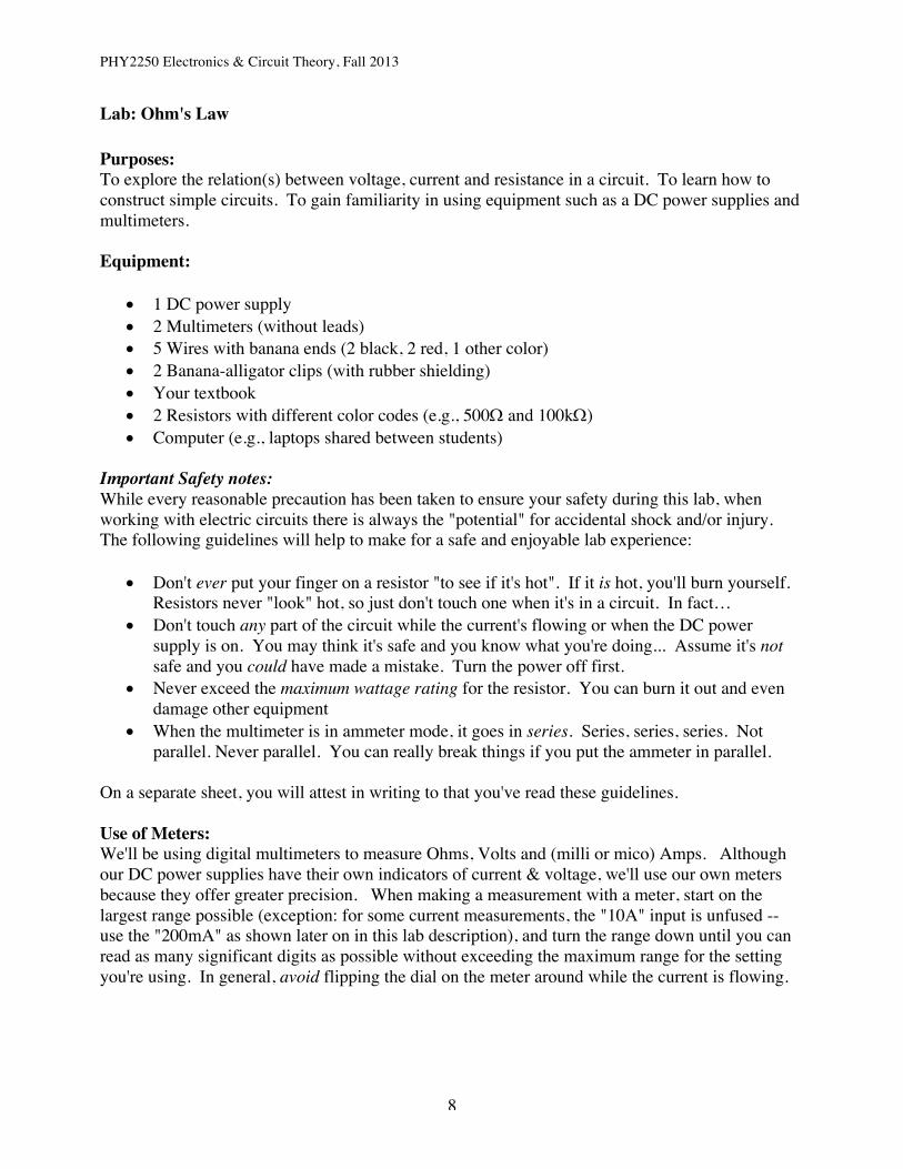
4. Next you'll measure current vs. voltage through the resistor via the following steps: a. Set up a circuit as shown in the diagram(s) below. Don't turn the power on yet!
Schematic diagram: "Physical" diagram (not to scale!):
b. Make sure the voltage and current knobs on the power supply are turned all the way counter-clockwise (zero voltage and current).
c. To avoid overloading the meters: Make sure the ammeter (multimeter set to "A") is on the maximum range for the 200mA setting, and the voltmeter (multimeter set to "V") is on the 200V range. Once the power is on, you may safely decrease the maximum range setting as needed.
d. Now you should be ready to go. Flip the power on the DC power supply and turn the current knob up about halfway. (If the current knob is not turned up high enough for a given voltage, you may end up "current limited".)
V/W COM 200mA 10A
#.## V A
W
AM
VM + -
DC Power
- + Volts Amps V I
#.## #.##
V/W COM 200mA 10A
#.## V A
W
Clip
!
Clip
!
Plugs in back
Plugs in back
Black
Black Red
Red
Blue?

PHY2250 Electronics & Circuit Theory, Fall 2013
10
e. Measure current through and voltage across the resistor for at least six values of voltage (never exceeding the maximum voltage). Write these in the spaces provided, being sure to keep track of the units (e.g. mA or µA).
f. Enter these values in an Excel Spreadsheet, and calculate the values of V/I for each pair of values. Also make an "XY Scatter" plot of V vs. I for these values.
g. Fit a line to your data: Right click on a data point, and select "Add Trendline" on the pop-up menu. Select "Linear" and under "Options", tell Excel to print the slope and intercept on the graph, as shown in the example graph (below). The slope of this trendline (the number before the "x") constitutes another measure of resistance.
h. Print out the graph (the printer is in HSB101) 5. Answer the questions on the following page. 6. Staple together your data sheet, answered questions, and graph printout(s) and turn them in.
You're finished!
Sample Data for Ohm's Law LabResistor 1 (R,R,R,Gold)R from color code (Ω): 2200Min R (w/in 5% Tolerance): 2090Max R (w/in 5% Tolerance): 2310Ohmmeter (Ω): 2200Max V for 0.5W: 33.16625
I (mA) I (A) V (V) V/I (Ω)0.409 0.000409 0.863 2110.0241.065 0.001065 2.22 2084.507
1.56 0.00156 3.04 1948.7183.18 0.00318 5.91 1858.4914.83 0.00483 9.28 1921.3255.99 0.00599 11.46 1913.189
Resistor 2 (Y,Blue,Y,Gold)R from color code (Ω): 4.70E+05Min R (w/in 5% Tolerance): 4.47E+05Max R (w/in 5% Tolerance): 4.94E+05Ohmmeter (Ω): 4.74E+05Max V for 0.5W: 484.768
I (µA) I (A) V (V) V/I (Ω)2.5 2.5E-06 0.972 3888008.9 8.9E-06 3.44 386516.923 0.000023 8.86 385217.4
36.4 3.64E-05 14.04 385714.369.1 6.91E-05 26.5 383502.2
V vs. I
y = 1890.1x + 0.0963R2 = 0.9994
0
2
4
6
8
10
12
14
0 0.002 0.004 0.006 0.008
Current (A)
Vo
ltag
e (V
)
V vs. I
y = 383371x + 0.0357R2 = 1
0
5
10
15
20
25
30
0 0.00002 0.00004 0.00006 0.00008
Current (A)
Vo
ltag
e (V
)

PHY2250 Electronics & Circuit Theory, Fall 2013
11
Ohm's Law Data Sheet Name(s)____________________________________________
Resistor 1: Color Code: ________ ________ ________ ________
R from Color Code: __________ +/- _________ R from Ohmmeter: ________________
Maximum Voltage for 0.5W: ______________
Voltage (units?) Current (units?)
Resistor 2: Color Code: _________ _________ _________ _________
R from Color Code: __________ +/- _________ R from Ohmmeter: ________________
Maximum Voltage for 0.5W: ______________
Voltage (units?) Current (units?)

PHY2250 Electronics & Circuit Theory, Fall 2013
12
Questions: Answer these as they apply to both resistors you measured. 1. How do your different determinations of resistance (color code, ohmmeter, V vs. I) agree or disagree? 2. Are the measurements within the tolerance value for the resistor(s)? 3. To what extent is Ohm's Law being obeyed or not? (e.g., is the graph of V vs. I at least linear?) 4. Do you notice any trends in the V/I ratio as you change the voltage? If so, what are they? 5. What might be responsible for the difference(s) in the resistance values you measured/calculated? 6. Which method for measuring resistance do you regard to be the most accurate? Why? Which is the least accurate and why? 7. Given these differences in resistance values, how would apply this knowledge when it comes time to design your own electronic circuitry?

PHY2250 Electronics & Circuit Theory, Fall 2013
13
Reference: Resistor Color Code
Colors: Digit Mnemonic (Make your Own)
Black 0 B________ Brown 1 B________
Red 2 R________ Orange 3 O________ Yellow 4 Y________ Green 5 G________ Blue 6 B________
Violet 7 V________ Gray 8 G________ White 9 W________
Tolerances: Gold +/- 5% Silver +/- 10% None +/- 20%
Example: A resistor with bands Red, Blue, Green, Silver.
Red Blue Green Silver 2 6 5 10%
= 26x105 ± 10% = 2.6x10⁶ ± 2.6x105 = 2.6 ± 0.26 MW.
First Digit Second
Digit
x Power of Ten Tolerance

PHY2250 Electronics & Circuit Theory, Fall 2013
14
Lab: Resistivity of Conductors - NOTE: Usually we skip this lab, and go on to Internal Resistance Purpose: To investigate the effects of wire length, cross-sectional area and Resistivity on the resistance of conductors Equipment:
• DC power supply, with a readout for current in Amperes • PASCO EM-8812 Resistivity Apparatus, and Wire Set • 1 DC Voltmeter • 4 Wires with banana ends • Your textbook: Electronics: A Complete Course by Nigel P. Cook • Computer (e.g., laptops shared between students)
Introduction: Recall that the functional dependence of resistance R on length !, cross-sectional area A and resistivity r is (supposedly) given by
€
R = ρA
.
The Apparatus: It has current-limiting resistors in it, and a 2 Amp fuse. You do not want to blow this fuse! The current-limiting resistors mean that the resistance of the wire sample will have only a small effect on the current in the (series) circuit. In fact, each wire sample will only acquire tens of millivolts and have a resistance of tenths of an Ohm. Below is a picture of the apparatus. You should NOT connect it until instructed to do so in the Procedure, below. Procedure: This lab will be conducted in three successive parts:
Part I: Variation of Resistance with Length 1. Choose the copper conductor with diameter D = 0.040 inches, which equals 40 mils.
(1 mil = 1 thousandth of an inch). Attach it to the Resistivity Apparatus in the following way:
a. Push the two "probe leads" all the way to the "outside" of the apparatus. b. Thread the copper wire under the probe leads and into the metal clamps at the
sides of the apparatus.
0 2 4 6 8 10 12 14 16 18 20 22 24
"Probe leads" (to voltmeter)
To DC Power Supply
screw clamp screw clamp wire sample

PHY2250 Electronics & Circuit Theory, Fall 2013
15
c. Screw the clamps down so that electrical contact is made. Note that power from the power supply will make direct contact with these clamps.
2. Hook up the leads of the voltmeter to the two probe leads, and use the "200mV" setting. 3. With the DC power supply off, connect the positive and negative terminals to the other
banana ports on the sides of the apparatus. 4. On the power supply, turn the voltage knob and the current knob all the way down, and
flip on the power switch for the supply. 5. We want to make sure we stay well below the 2A limit on the Resistivity Apparatus.
So adjust the voltage and current knob so that the readout on the power supply reads 1.5 Amperes. You can now leave the power supply at these settings for the entire lab. There is no need to adjust the power supply settings in the exercises that follow.
6. Now set the left probe lead at zero centimeters. By placing the right probe lead at different locations spaced out along the length of the conductor, take six voltage readings from the voltmeter. (We recommend 2cm, 4cm, 8cm, 14cm, 19cm and 24cm, but you may use other values.) These will likely range from 0.5 mV to 8mV.
7. Using the current of 1.5A and Ohm's Law, convert your voltage readings into resistance values.
8. Make a plot of resistance R vs. the length ! of the conductor. You may want to express the resistance in Ohms and the length in feet (1 inch = 2.54 cm, 1 foot = 12 inches) before making the chart.
9. Fit a trendline to this, and for "Options," select "Set intercept y = 0" and "Display Equation on Chart".
10. The slope of this line gives you a measure of R/!, which you can then multiply by the cross sectional area A = (40 mil)2
= 1600 cmil, to get the resistivity r. Part II: Variation of Resistance with Area
1. Disconnect the power supply. Now slide the probe leads to the far sides of the apparatus, unscrew the clamps and remove the copper.
2. Select the thinnest brass wire (D = .020 in = 20 mil) and attach it as you had the copper. Reconnect the power supply, and note that the current reading on the power supply is probably no longer 1.5A. This is to be expected. Just make a record of the current value every time you switch the wire sample, but do not adjust the power supply.
3. Set the probe leads to "0 cm" and "24 cm", and measure the voltage across the wire. 4. Repeat 1-3 with the other three gauges of brass wire, making sure to record the current
from the power supply each time. Use the same length of wire for each sample. 5. Noting that cross-sectional area in "cmil" is simply the square of diameter in mils,
compute the reciprocal of the area, 1/A, for each of these wire gauges. 6. Using your voltage and current readings, compute resistance values for each brass wire. 7. Make a plot of R vs. 1/A, and fit a line to it. 8. Similarly, you can take the slope of this line, divide by the length of the wire !, and find
the resistivity r.
Part III: Variation of Resistivity with Material Repeat the method for Part I, using aluminum and nichrome wires as well, i.e. plot resistance vs. length for each of these. Remember to have the power supply disconnected when attaching the wires and screw clamps! Calculate resistivities for both materials.
Conclusions: Answer the questions which follow the data sheet.

PHY2250 Electronics & Circuit Theory, Fall 2013
16
Sample Data: Part I: R vs. L for CopperCurrent (A) = 1.5
L (cm) V (mV) L (ft) R (Ohms)2 0.6 0.06562 0.00044 1.3 0.13123 0.000866678 2.6 0.26247 0.00173333
14 4.5 0.45932 0.00319 6.1 0.62336 0.0040666724 7.8 0.7874 0.0052
Slope (Ohm/ft) = 0.00657D (mil) = 40A (cmil) = 1600rho (Ohm cmil/ft) = 10.5
Part II: R vs. 1/A for BrassLength (cm) = 24
D (mil) I (A) V (mV) 1/A (1/cmil) R (Ohms)20 1.31 115.7 0.0025 0.08832132 1.44 47.4 0.00097656 0.03291740 1.45 30.8 0.000625 0.02124150 1.45 20.3 0.0004 0.014
Slope (Ohm*cmil) = 35.054Length (ft) = 0.78740157rho (Ohm cmil/ft) = 44.5
Part III: R vs. L for Aluminum & Nichrome, D=40 mil
Aluminum:Current (A) = 1.45L (cm) V (mV) L (ft) R (Ohms)
2 1.7 0.06562 0.001133334 3.5 0.13123 0.002333338 7 0.26247 0.00466667
14 12.2 0.45932 0.0081333319 16.6 0.62336 0.0110666724 21 0.7874 0.014
Slope (Ohm/ft) = 0.0178rho (Ohm cmil/ft) = 28.5
Nichrome:Current (A) = 1.04L (cm) V (mV) L (ft) R (Ohms)
2 20.9 0.06562 0.013933334 41.5 0.13123 0.027666678 82.2 0.26247 0.0548
14 143.4 0.45932 0.095619 194.8 0.62336 0.1298666724 246 0.7874 0.164
Slope (Ohm/ft) = 0.2083rho (Ohm cmil/ft) = 333
y = 6.57E-03x
0
0.001
0.002
0.003
0.004
0.005
0.006
0 0.2 0.4 0.6 0.8
L (ft)
R (
Ohm
s)y = 35.054x
0
0.01
0.02
0.03
0.04
0.05
0.06
0.07
0.08
0.09
0.1
0 0.001 0.002 0.003
1/A (1/cmil)
R (
Ohm
s)\
y = 0.0178x
y = 0.2083x
0
0.02
0.04
0.06
0.08
0.1
0.12
0.14
0.16
0.18
0 0.2 0.4 0.6 0.8
L (ft)
R (
Ohm
s) Aluminum
Nichrome
Linear(Aluminum)Linear(Nichrome)

PHY2250 Electronics & Circuit Theory, Fall 2013
17
Resistivity Data Sheet Name(s)___________________________________________ (You may record values directly to a spreadsheet if you wish, provided it is will-annotated.) Part I: Resistance vs. Length (Copper)
Current = __________________.
Position Voltage
Slope from line fit = ___________________ (units?)
Cross-Sectional Area = _________________ cmil
Resistivity of Copper (measured) r = _______________________ Part II: Resistance vs. 1/Area (Brass)
Diameter Current Voltage
Slope from line fit = ___________________ (units?)
Length of Wire = _______________ inches
Resistivity of Brass (measured) r = ________________
Part III: Resistivity vs. Material Repeat resistance vs. length measurements as in Part I, and find resistivities for:
Aluminum, D = 40mil: r = _____________________
Nichrome, D = 40mil: r = ______________________.

PHY2250 Electronics & Circuit Theory, Fall 2013
18
Questions:
1. Was R vs. ! linear? 2. What about R vs. 1/A? 3. In what sense was the equation R = r!/A confirmed or disproved?
4. Compare the resistivity values you measured with those listed in your textbook. How well do they agree or disagree? Be specific.
5. Anything suggestions that would make this lab more interesting and/or "relevant"?
PHY2250 Electronics & Circuit Theory, Fall 2013
19
Lab: Internal Resistance Purposes:
• To gain some experience with series circuits • To demonstrate that "real world" components, while not perfect, at least have measurable
deficiencies Equipment:
• 1 Voltmeter • 1 Ammeter • One voltage source, e.g. "D" Dry Cell Battery • Variety of resistors, e.g. a resistor bank
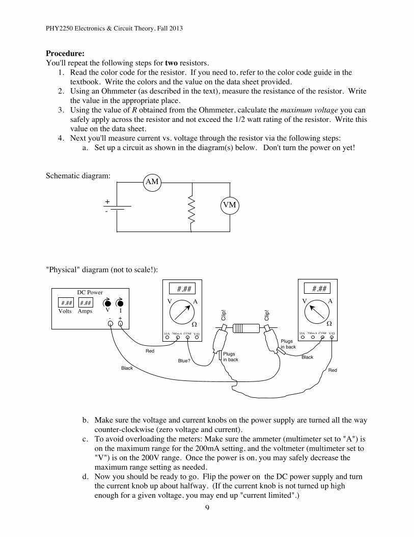
Introduction: The setup will be essentially the same as the Ohm's Law lab, however we will use a battery instead of a DC power supply. The EMF (voltage) of the battery will be represented by E, and its internal resistance r, in the circuit below: We will neglect the small amount of current which flows through the voltmeter, and the small resistance of the ammeter. One of the important concepts in series or parallel circuit analysis is Kirchoff's Loop Rule: The sum of the voltage changes around any closed loop (in a circuit) is zero. If we regard voltage sources as positive changes in voltage, and resistors and negative changes (of amount -IR), then, starting in the lower left corner of the circuit diagram, the sum of the voltage changes around the loop containing the load resistor can be written as
€
E − Ir − IR = 0 . But IR is the same as the potential difference measured across the load resistor, V. Thus we can rearrange the above expression as
€
V = −rI + E . Note that this has the form of a linear equation, y = mx + b. Procedure:
1. Set up the circuit in a similar manner to that of the Ohm's Law lab. 2. Vary the load resistance R in the circuit (you do not need to record the resistances) and
record various readings of the current I and the potential difference across the load resistor, V.
3. Make a graph of V vs. I (i.e. voltage on the y axis, current on the x axis). 4. Fit a line to the graph, and record the slope and y-intercept of this line. These tell you the
"ideal" EMF of the battery, E, and the internal resistance of the battery, r! 5. Print out the graph, answer the questions on the data sheet.
AM
VM + -
R r
E
I V

PHY2250 Electronics & Circuit Theory, Fall 2013
20
Internal Resistance Lab Name(s): ____________________________________ Data Sheet
Current Reading (units?) Voltage Reading (units?)
Slope of graph (units?): _______________ y-intercept (units?):______________ Questions: 1. What is the internal resistance of your battery? 2. What is E, the "ideal" EMF of the battery? 3. Given these two quantities, what is the theoretical maximum current that could be supplied by the battery? (Consider a short circuit connecting the two ends of the battery.) 4. What is the maximum power that can be delivered by the battery? (𝑃#$% = 𝐸(/(4r) ). 5. How does the internal resistance affect the voltage produced by the real battery as a source produces more current? Why does a new 1.5 volt AA battery yield a reading of about 1.60 Volts when not in a circuit?

PHY2250 Electronics & Circuit Theory, Fall 2013
21
Pre-Lab: Breadboarding & Loaded Voltage Divider Name:________________________ 1. When laying out a circuit on a breadboards, the objective is a) visual clarity b) looking cool c) use long wires d) using as few jumpers as possible 2. Make a guess as to why we bother with insulated jumper wires at all --- why not just use bare wire everywhere? 3. We'll be using a R1 as a "current limiter" (instead of a fuse). If the power supply is set to VS = 10V, and we want to make sure that, no matter what R2 or R3 we plug in, we'll never exceed the 1/4 Watt rating of the resistors, then what minimum value does R1 need to be? 4. Let's say our input is 10V and we want (ideally) 4V for Vout,("ideally" implying the open-circuit output voltage in which R3=infinity). What should we use for R2 (using the R1 value found in #3)? 5. What's the maximum possible Vout you can get, given a Vs of 10V (and using the R1 value found above)?

PHY2250 Electronics & Circuit Theory, Fall 2013
22
Lab: Breadboarding & Loaded Voltage Divider Purpose(s):
• To gain practical experience designing, building and testing series-parallel circuits. • To see how "load" can affect the performance of a circuit • To gain familiarity and facility with circuit construction using solderless prototyping
boards, i.e. "breadboards"
Equipment: • Solderless Breadboard • Wires & Alligator Clips • Regulated DC power supply • Assortment of resistors of various values • Multimeter(s)
Introduction: For the remainder of this course, we will build our circuits using solderless "protoboards" or "prototyping boards," typically called "breadboards." The holes in the breadboard are connected in short columns or long rows by conducting strips beneath the board:
The holes in each set of 5 holes are connected "vertically" in a column. Bus lines/strips. Each bus line is connected as a row. Note that the bus lines are only half the length of the board.
Breadboard Etiquette Convention has it to use the bus lines chiefly for power distribution, i.e. connect the + terminal of the power supply to the top bus line, and the - terminal to the bottom bus line. Components are connected by using holes sharing the same column, and/or via the use of (ideally short) wires called jumpers. The efficient and neat physical layout of circuit elements is essential to building intelligible and troubleshoot-able electronic circuitry. Refer to pp. 45-47 of the text for such examples. Long wires are to be avoided, because they make for "spaghetti" circuits, making it hard to visually follow signal flow.

PHY2250 Electronics & Circuit Theory, Fall 2013
23
The use of colored jumper wires is encouraged, in order to "label" certain functions (e.g., red for positive, black for negative), and/or to visually group common elements of a circuit together. Also, it is best to avoid "crossing" jumper wires and/or components whenever possible, again because crossing inhibits easy visual comprehension of current flow. Jumpers are typically used such that they are flat (or nearly flat) against the breadboard whenever possible. Also, it is good to add "jumpers with one end free" to make it easy to connect/disconnect peripherals such as power supplies and meters (via clipping them to the free end of the jumper wire), that circuit components are not subjected to undue mechanical stress. There is not a hard line of "right" and "wrong" when building a circuit with a breadboard, however the goal should be to maximize visual clarity so that an outside observer can easily and quickly determine your circuit layout and follow the path(s) of current. The Voltage Divider In this lab we will study the behavior of a voltage divider circuit under different loads. The circuit shown below is a prototypical voltage divider.
Procedure: 1. Designing the Circuit: Set Vs=10V. Select a resistor for R1 which is at least as large as the value you found in the prelab. Select a resistor for R2 which will place Vout between 3.5V and 4V. Measure these resistors with an ohmmeter, and calculate the expected value of Vout. Show your calculations below:
R1=_____________________ R2=____________________
Expected Vout=_________________ 2. Measurement. Build the circuit shown above and measure the voltage and current through the circuit:
Vout=_____________________ IT=____________________
VM
AM R1
R2
Vs
Vout

PHY2250 Electronics & Circuit Theory, Fall 2013
24
3. Loading the divider. Now you will place third resistor, R3, in parallel with R2, and measure the current I and voltage Vout. Do this for five values of R3 (measured with an ohmmeter!), e.g. 10kW down to 100W and record the results below.
R3 Vout IT 4. Analysis: Make two plots, one of Vout vs. R3 and another of I vs. R3. Conclusions: 1. How did your expected Vout agree or disagree with the value of Vout you measured for the unloaded (no R3) voltage divider? 2. How does the output voltage (Vout) vary as you change the load (R3) on the divider? Be as specific as possible. 3. How does the current required of the power supply (I) vary as you change the load (R3) on the divider? Be as specific as possible. 4. How does the current through R2 vary as you change the load? (Note I2 = Vout / R2) 5. Reflect on Sal Greco's saying, "You need enough I to keep the V across the R" in the context of this "loaded" voltage divider example.

PHY2250 Electronics & Circuit Theory, Fall 2013
25
Pre-Lab: Oscilloscope Orientation Name:________________________________ 1. Your 'scope is set to 0.2V/div and 5ms/div. Draw an example of the oscilloscope trace for a sine wave with amplitude 0.65V and period 30ms:
Note that in this example, we have used the maximum Volts/div and Sec/div settings which still allow this (particular) complete waveform to be seen -- i.e. that make it "biggest" on the screen. Such settings allow us to make the most accurate readings of our signals, and should be used as a matter of habit when using the 'scope: Always make the signal as "big" as possible, to get the most accurate readings. 2. After hooking up your source to the scope on Channel 1, you see only a straight line rather than an AC signal. Which of the following could be the source of this problem?
a) Selector switch set to "GND" instead of "AC" b) Channel selector set to "Ch2" instead of "Ch1" c) Time/Div switch set at too low (i.e. too fine) of a setting d) Bad scope lead e) Any of the above
3. Your input is a triangle wave of frequency 50Hz and amplitude 500mV. Decide on two different combinations of Volts/div and Time/div settings (which may or may not maximize the "size" of the image waveform), and draw the signal you'd see at each of these settings:
4. Explain the effect on the oscilloscope trace of adjusting the triggering level and selecting the triggering slope. Also, describe the sort of picture are you likely to see if the trigger level is set at the maximum or minimum (i.e. amplitude) of a sinusoidal signal.
Volts/div: _______________
Time/div: _______________
Volts/div: _______________
Time/div: _______________

PHY2250 Electronics & Circuit Theory, Fall 2013
26
Lab: Oscilloscope Orientation Name(s):________________________________ Purpose: To gain facility in the use of the oscilloscope for measuring properties of AC circuits Equipment:
• Oscilloscope, e.g. BK Precision 2120 • Signal Generator • Oscilloscope probe and/or something to go from BNC connector ('scope input) to banana plug (signal
generator output) Introduction/About the Scope: The oscilloscope is essentially a voltmeter --- the voltage of a signal is directly linked to the voltage which causes electrons in the 'scopes cathode ray tube (CRT) to deviate in the vertical direction. The speed at which the electron beam sweeps across the screen is set by the "Time" (or "Sec/Div") knob. There are lots of knobs and switches on the scope. Their operation is described in our textbook and the 'scope manual. The key knobs and switches you'll be using are shown below:
Our oscilloscopes are analog (as opposed to digital) scopes, and their operation is "manual"; that is to say, they do not automatically select the appropriate scale (so-called "auto scale") nor do they have an automated frequency analyzer to tell you what the frequency of your signal is. Rather, we will select our scales manually such that the maximum deviation of the scope trace is visible for a given voltage, and that no more than one (complete) period of oscillation is visible on the trace. As a voltmeter, the oscilloscope has a very large impedance, (which is like resistance), meaning that it can be hooked up in parallel to a circuit element and very little current will flow. If, however, the circuit component you are measuring has itself a very large impedance (e.g. a 1MOhm resistor), then hooking up the scope can distort the operation of the circuit you are trying to measure. For most of the circuits we cover in this course, this will not be a problem, but you should keep this in mind whenever you are measuring a high-impedance source. The two principal inputs on the scope are two BNC (bayonet Neil-Concelman) connectors. The BNC connector is a type of RF connector used for terminating coaxial cables. The cables we will use will terminate on the other end with either an oscilloscope probe, a pair of alligator clips, or a pair of banana plugs. For each of these "probe-like" ends, there will be a positive side and a "ground" side. Often you only need to use the positive side, because…
Intensity
Power
Trig. Lev. Focus
AC
DC GND
AC
DC GND
Vert. Pos. Vert. Pos. Horiz. Pos.
Ch1 Ch2
Add Dual
Cal
V/Div V/Div
Sec/Div
Source Ch1 Ch2
Aux E/M
Ch1 Ch2
Mode
Ch1 In Ch2 In
'SCOPEY '08 Var Sweep
PHY2250 Electronics & Circuit Theory, Fall 2013
27
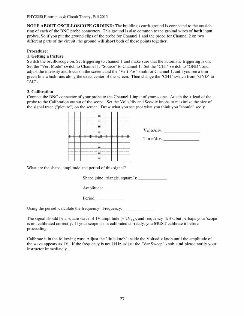
NOTE ABOUT OSCILLOSCOPE GROUND: The building's earth-ground is connected to the outside ring of each of the BNC probe connectors. This ground is also common to the ground wires of both input probes. So if you put the ground clips of the probe for Channel 1 and the probe for Channel 2 on two different parts of the circuit, the ground will short both of those points together. Procedure: 1. Getting a Picture Switch the oscilloscope on. Set triggering to channel 1 and make sure that the automatic triggering is on. Set the "Vert Mode" switch to Channel 1, "Source" to Channel 1. Set the "CH1" switch to "GND", and adjust the intensity and focus on the screen, and the "Vert Pos" knob for Channel 1, until you see a thin green line which runs along the exact center of the screen. Then change the "CH1" switch from "GND" to "AC". 2. Calibration Connect the BNC connector of your probe to the Channel 1 input of your scope. Attach the + lead of the probe to the Calibration output of the scope. Set the Volts/div and Sec/div knobs to maximize the size of the signal trace ("picture") on the screen. Draw what you see (not what you think you "should" see!): What are the shape, amplitude and period of this signal?
Shape (sine, triangle, square?): _____________ Amplitude: ____________ Period: ____________
Using the period, calculate the frequency. Frequency: ______________ The signal should be a square wave of 1V amplitude (= 2Vp-p), and frequency 1kHz, but perhaps your 'scope is not calibrated correctly. If your scope is not calibrated correctly, you MUST calibrate it before proceeding. Calibrate it in the following way: Adjust the "little knob" inside the Volts/div knob until the amplitude of the wave appears as 1V. If the frequency is not 1kHz, adjust the "Var Sweep" knob, and please notify your instructor immediately.
Volts/div: _______________
Time/div: _______________

PHY2250 Electronics & Circuit Theory, Fall 2013
28
3. Measuring General Signals 3.1- With your signal generator turned off, hook up the input of the scope to the output of the signal generator. Turn the amplitude of the signal generator all the way the zero setting (which is all the way counterclockwise) and turn it on. Set the shape to sine wave, the frequency to 800Hz, and turn up the amplitude about a quarter turn (or less). Draw what you see: What are the amplitude and period of this wave?
Amplitude:______________ Period:________________ 3.2 - The x5 switch - Now pull out the little knob in the middle of the Channel 1 Volts/Div knob. What happens to the picture? i.e., what changes and what does not change? 4. Additional Questions 4.1 - How would you measure a DC signal using an oscilloscope? 4.2 - We didn't talk about multi-channel input modes, e.g. X-Y mode, summing, and so forth. What would you like to learn about these, and in particular, what uses for multi-channel scope tracing might you find in audio engineering applications?
Volts/div: _______________
Time/div: _______________

PHY2250 Electronics & Circuit Theory, Fall 2013
29
Lab: RC Circuits Name(s):__________________________________ Purpose: To observe the response of series RC circuits to both DC and AC sources. Equipment:
• AC Signal Generator • Oscilloscope and probe • Resistor and a ceramic capacitors (e.g. 11nF) • Computer with Excel • Digital Multimeter
Part 1: DC Circuits In this first part, we will investigate the charging and discharging of a capacitor in a DC circuit. Procedure: Select a capacitor and resistor, e.g. 11nF and 2200W, respectively. Measure the resistance and capacitance using a multimeter, and write them here: R: ________________ C:________________ Use these to compute the value of your RC time constant t. t = ________________. Build the following circuit: Use your signal generator as Vsource and connect oscilloscope Channel 1 across it. Use Channel 2 as Vout, i.e. the voltage across the capacitor. Set the signal generator to square wave, with a period several times larger than your RC time constant, e.g. around 10 kHz. Set the scope to dual trace, triggering on channel 1. Set both Ch1 and Ch2 on the same number of volts/div, while maximizing the size of the waveform(s) --- you can set the "zero" to be a line near the bottom of the screen, rather than the center line. Draw a picture of what you see on Channel 2.
~ Vsource
Vout
Settings: V/div: ______________ Sec/div: ______________

PHY2250 Electronics & Circuit Theory, Fall 2013
30
Now, using the discharging phase of the oscillation, on Channel 2, take several values of the voltage at different times from at beginning of the discharge (t=0), and write them on the following table:
Time t Voltage V
0
We expect the discharge phase of the capacitor's cycle to go as
€
V = V0 exp(−t /τ ). Dividing by Vo and taking the natural log of both sides, we find
€
ln VV0
"
# $
%
& ' = −
1τt .
Using Excel, make a graph of ln(V/V0) vs. time. Fit a line to it and take its slope. The inverse of this slope will be a measure of your time constant t.
t (experimentally determined): ___________________. Question: How does this value of t correspond to the value obtained at the beginning of the lab? Part 2: AC Circuits - the Low Pass Filter When the signal oscillates too rapidly, the capacitor does not have sufficient time to charge completely, resulting in a decreased output for the capacitor. The "turn-over" frequency at which this begins to occur is given by
€
f0 =12πτ
=1
2πRC.
Calculate what you expect your turn-over frequency to be in Hz:
f0 = ____________________.
The general behavior or amplitude response from the filter is given by the gain G, which is the ratio of the output amplitude to the source amplitude:
€
G =Aout
As
=1
1+ ff0
" # $ %
& ' 2
= V0

PHY2250 Electronics & Circuit Theory, Fall 2013
31
Procedure: Now switch the signal generator to sine wave. Start the sine wave at a very low frequency f<< f0 and choose some input voltage, e.g. 1V (amplitude or peak-to-peak; just be consistent below…). For several widely-spaced values of the input frequency (e.g. 20Hz to 90kHz), record the output voltage. Record a few extra frequencies/voltage pairs around f0. Record them on the following table on the following page. (You may simply record the frequency reading from the signal generator.)
Frequency (Hz) Vout
20
90000
Take your values and plot them on a log-log plot of Vout vs. frequency. If necessary, create extra columns in which to calculate log10(f) and log10 (Vout). Print out the graph and staple it to your report. Questions: Referring to your graph, what happens for f< f0? What happens for f> f0?
And how would you describe the voltage output (or gain) near f0?

PHY2250 Electronics & Circuit Theory, Fall 2013
32
Lab: Loudspeaker Impedance Name(s):____________________________
Equipment: • Two multimeters • Loudspeaker • Resistor, 5 – 30 Ohms, preferably 10 Ohms. • Signal Generator
Recommendation: *Bring earplugs for this lab*
Background: A loudspeaker presents a load which a combination of inductive reactance (due to the coil that makes up the electromagnet), resistance (due to the wire in the coil having a finite resistance), and mechanical impedance (due the mechanical process of pushing the cone in and out against air resistance). These three combine to form the overall speaker impedance ZSp. In this lab, we will measure ZSp, the impedance of a loudspeaker, as a function of frequency. We will do this by placing it in series with a resistor R and measuring the voltages VR and VSp across the resistor and speaker, respectively. With this information, we can compute ZSp by noting that the relative lengths of the voltage vectors are similar to the relative lengths of the impedances (think of the impedance diagram and voltage diagram), i.e. R / VR = ZSp / VSp. In other words,
𝑍/0 = 𝑅𝑉/0𝑉3.
red
black
R
Sp VSp
VR
R
ZSp
VR
VSp

PHY2250 Electronics & Circuit Theory, Fall 2013
33
Procedure:
1. Before building the circuit, first use the ohmmeter setting on a multimeter to measure R, the resistance of your resistor, and (separately) RSp, the resistance of the loudspeaker:
R = ___________ Resistor, RSp =____________ Speaker Resistance
2. Now build the circuit: Place the resistor in series with the loudspeaker, and attach the signal generator across this combination, as shown in the schematic. Set both multimeters to AC volts. Place one meter across R to measure VR, and the other meter across the speaker to measure VSp.
3. Turn the amplitude knob a quarter-way up on the signal generator. 4. By varying the frequency and reading voltages using the meters, record (simultaneous)
values for VR and VSp, for frequencies from 10 Hz to 10000 Hz, choosing frequency values that are farther spaced apart as you increase the frequency – you will ultimately be using a logarithmic scale for frequency. Note: Do not simply choose frequency values a priori, but rather choose your values as you follow the shape of the graph, getting multiple values below 100 Hz where it curves the most. Get 18 points in all. Cautionary note: make sure to get at least 3 digits of precision for all measurements, especially for VR.
5. Calculate ZSp, the impedance of the speaker for all frequencies, using the formula on the previous page.
6. Make a plot of ZSp vs. log frequency. (See sample data, below..
Question(s): 1. How do the values of ZSp shown in your graph compare with the value of RSp? 2. At what (“low”) frequency is the speaker impedance a local maximum? 3. Why do you think your speaker is “rated” at 8 Ohms by the manufacturer?
Sample Data:
Quote: ‘A speaker is not linear 8 ohms at all frequencies. We did this [test] at Prince’s [studio]. The JBL 18” in the mains were rated at 600 watts 8 ohm, however the impedance dropped to 2 ohms at 60 Hz flowing A LOT more power at 60 Hz. No wonder the JBLs were so punchy because they flowed over 2000 watts at 60 Hz. This is also why Prince could literally blow the cone out of the basket. I had 18 spares to keep 8 in service.’
-- Sal Greco, Head Engineer, Belmont OceanWay Studios. Formerly head engineer for Prince.
0
2
4
6
8
10
12
14
16
10 100 1000 10000
Z_Sp(Ohm
s)
Frequency(Hz)

PHY2250 Electronics & Circuit Theory, Fall 2013
34

PHY2250 Electronics & Circuit Theory, Fall 2013
35
Lab: Transformers Purpose: To investigate the practical application of magnetic induction, become acquainted with the construction and operation of transformers. Equipment:
• PASCO™ Basic Coil Set • AC Power Supply / Signal Generator • 2 Digital Multimeters • Solderless Breadboard • 8-Pin Iron Core Transformer • Resistors of various values • Wires w/ banana plugs • Alligator clips
Part I: Transformer Construction The ideal output of a transformer is given by the formula
€
V2 =N2
N1V1 (1)
where V2 is the secondary voltage, N2/N1 is the turns ratio of the transformer, and V1 is the primary voltage. In real life, this ideal is rarely realized. In this section of the lab, we will see how close we can come to it, by varying the construction of the transformer. Procedure: 1. With the signal generator off, set the Digital Multimeter to AC Volts (20V range) and connect it to the signal generator. Turn the signal generator on, set it to sine wave and 1000 Hz. Adjust the amplitude of the AC source until it registers 6V on the multimeter. Turn off the signal generator and disconnect the multimeter. 2. Using wires & alligator clips, put a resistor of RS=100W and an ammeter in series with the (N1=)400-turn coil, and connect this combination across the signal generator. 3. Connect a resistance of approximately RL=100W across another coil with turns N2. Using the other multimeter, measure the voltage V1 across the primary coil (note that it won't be 6V due to the resistor), and then the voltage V2 across the secondary. Record this on the data sheet provided. 4. Make measurements for two different secondary coils, for the air core transformer shown above, as well as the following transformer configurations:
AC Generator
"Air Core"
N1 N2 RL RS
"Single Rod" "U-Shaped" "Ring-Shaped"
AM

PHY2250 Electronics & Circuit Theory, Fall 2013
36
5. Using your measurements of I1, your measurements of V2 and your measured value of the resistor RL (using the ohmmeter), calculate I2 (=V2/R2) and the ratio I1/I2. Part II: Frequency Response, using "Real" Transformers We have a set of ring-shaped transformers which can be pressed into solderless breadboards. These transformers have eight leads, arranged and numbered from 1 to 8. We'll be using the transformer "backwards" and stepping up the voltage. Using jumper kits, connect leads 2 and 3 together. Hook the source voltage across leads 5 and 6, and the load resistance across leads 1 and 4. The following diagram shows the final configuration: Fix the AC signal fixed at some voltage (or just leave it at 6V), press the "range" buttons on the signal generator to record the primary and secondary voltages for 10Hz, 100Hz, 1000Hz, and 10000Hz. Part IV: Impedance Matching
€
N2
N1=
ZL
Zs
(2)
Depending on time, we may or may not be able to do this in lab. A separate handout will be distributed for this section if it is undertaken.
2
3
4
6
7
8
~ 1 5 V1 = VS (Input!)
RL VM V2

PHY2250 Electronics & Circuit Theory, Fall 2013
37
Transformer Lab Data Sheet Name(s):_______________________________________
Part I: Transformer Construction RS = _____________ RL = _____________
Core N1 N2 V1 (meas.) Not 6V!
V2 calc'd,
=V1N2/N1
V2 (meas.)
V2/V1 I1 (meas.)
I2 =V2/RL
I1/I2
Air 400
Air 400
Air, 90o
Rod 400
Rod 400
U 400
U 400
Ring 400
Ring 400
Questions: 1. How did varying the construction of the transformer affect its output? 2. How do your output voltage (V2) values compare with the ideal expectation (Eq. (1))? 3. How did the ratios V2/V1 and I1/I2 compare? 4. Why do you think V1 changed even though you weren't changing the amplitude of the source? Part II: Frequency Response, using "Real" Transformers
N2 / N1 = _________________
Frequency (Hz) V1 (meas.) V2 (meas.) V2 / V1
10
100
1000
10000
Question: How would you describe the frequency response of the transformer?

PHY2250 Electronics & Circuit Theory, Fall 2013
38
Lab : Diodes & DC Power Supplies Name(s):____________________________ Purpose: To gain hands-on experience in constructing AC-to-DC power conversion circuitry using semiconductor components. Overview: In this lab, we will start with a simple half-wave rectifier and build up to a DC power supply using a bridge rectifier and capacitive filter. We will also do some thinking about the use of voltage regulators! Equipment:
• AC signal generator • Oscilloscope and probe(s) • Solderless breadboard • 4 Diodes • 1 Resistor, 100W • 2 Capacitors: one "small" (10 µF) and one "large" (1mF)
Part I: Half-Wave Rectifier Build the circuit below, and draw the source and output voltages on the grids provided. For the source voltage, use a sine wave with amplitude 5V at a frequency of 1kHz. Use "DC" on the scope. Question: 1. What do you measure the voltage drop across your diode to be?
~ Vsource
Vout
Volts/div: _______________
Time/div: _______________
Volts/div: _______________
Time/div: _______________
Vsource Vout

PHY2250 Electronics & Circuit Theory, Fall 2013
39
Part II: Full-Wave Rectifier Now construct the bridge rectifier shown below and, using the same source settings, graph the output voltage. Note: It's best to use a "step up" transformer to make sure there is plenty of voltage to drive the secondary circuit.
Part III: Filtered Power Supply Now insert a small capacitor to function as a "filter" in the circuit you just built, as shown below. Graph the output voltage. Then do the same for a larger capacitor.
Volts/div: _______________
Time/div: _______________
Vout
Volts/div: _______________
Time/div: _______________
Vout - Small C
Volts/div: _______________
Time/div: _______________
Vout - Large C
Vout
~ Vsource
Vout
~ Vsource
5
6
1
4
2 3

PHY2250 Electronics & Circuit Theory, Fall 2013
40

PHY2250 Electronics & Circuit Theory, Fall 2013
41
Questions: 1. For the small capacitor, what is the maximum voltage obtained by the filtered full-wave signal? What is the minimum voltage? 2. What are the effects of increasing the capacitance in the filter? Part IV: Thinking about Regulators A voltage regulator can be a Zener diode or an integrated circuit (IC) regulator chip. It's designed to keep the voltage from exceeding a certain value, by allowing more current to flow through it at large voltage values and "shunting" it away from the load. If you don't put the minimum required voltage across the regulator, very little current will flow through it and, for the purposes of the power supply, it will function like an "open" circuit element. Put differently, you need as much or more voltage across the regulator than it is rated, for it to do anything in your power supply. So, for example, if you want a regulated 4.5V, you would need to supply 4.5V or more --- up to some limit; regulators are only rated to within a certain maximum voltage rating, beyond which they burn out Question: 1. Say you want to use a voltage regulator, but for some reason you don't include a capacitive filter before the regulator, and instead try to regulate the "bare" full-wave-rectified signal. Try to figure out what output you'd expect to see if the full-wave-rectified signal has a peak voltage of 5V and your regulator is rated at 3V, and graph this output below. (Assume a sine wave for the AC source voltage.)
Volts/div: _______________
Vout

PHY2250 Electronics & Circuit Theory, Fall 2013
42
Lab: Transistors & Simple Amplifier Name(s):______________________________ Purpose: To investigate the "variable resistor" properties of transistors, using them to construct a simple amplifier. Equipment:
• Oscilloscope & two probes. (All voltage measurements will be made via the scope, e.g. in "DC" mode)
• Ohmmeter • DC Power Supply • AC Signal Generator • Transistor • Capacitor (any size) • 4 resistors. (Suggested values: R1=560W, R2=100W, RC=560W, RE=100W)
Procedure: We will build this amplifier, shown below, in a series of stages, labeled Parts I-IV. I. Building the 1st Voltage Divider We will operate the transistor within its "active region", i.e. with a base voltage somewhere in between OV ("off") and VCC ("saturation"). To do this, we will use a voltage divider (circled region in diagram) to bias the transistor's base ("B" in the diagram). To begin, we will build only the voltage divider part of the circuit. (Don't hook up anything else.) Using your knowledge of voltage dividers in DC circuits, and a supply voltage of 10V, select two resistors (R1 and R2) to produce a voltage across R2 which is around VCC / 4. Write these measured resistor values below:
R1 = _________________ R2 = ______________ Build the voltage divider and measure the voltage across R2. This will be (roughly) the voltage at the transistor's base. Write that below:
VB = __________________
~ Vsource
Vout
VCC = +10V
R1
R2
RC
RE RL
C1
B C
E
Part I Part II
Part III
Part IV
Hi W out
Q1

PHY2250 Electronics & Circuit Theory, Fall 2013
43
II. Adding the "2nd Voltage Divider", i.e. the Transistor We will now add a second voltage divider to the circuit, but this one will contain a transistor, which will function as a variable resistor, and will result in a variable voltage divider, where the output of this second divider is measured across Q1 (the transistor) and RE. To achieve this, you will need to select resistors RC and RE. The second "voltage divider" is inverted, so you want an RC
which is "large" (say 500W) and an RE which is smaller (100W should suffice). Hook up the resistors and transistor to the power supply, taking care to match up the "E", "B" and "C" printed on the transistor with the appropriate parts of the circuit. Connect the base to the output of the first voltage divider. Your transistor should be on! Measure the voltage at the collector ("C" in the diagram), and write it below:
VC = __________________ III. Supplying an AC Signal Now connect the "high impedance" output AC signal generator to middle of the voltage divider. Thus we will add the AC sine wave to VB, resulting in a varying voltage applied to the transistor. This will cause the transistor's resistance to vary, which will cause VC to vary. Using the same DC settings for base and collector, draw the signal you see at these two terminals: IV. Stripping the DC Bias Now we will add the capacitor and load resistor, as shown in the schematic. The load resistor should be large, 10K or more. The capacitor may be either an unpolarized or a polarized capacitor. If it is polarized, make sure you line up its polarity properly! Question 1: We are looking at AC signals, and yet we may use a polarized capacitor, which requires current to always flow in the same direction. Why are we "okay" in using a polarized capacitor with our (amplified) AC signal?
Volts/div: _______________
Time/div: _______________
Volts/div: _______________
Time/div: _______________
VB VC

PHY2250 Electronics & Circuit Theory, Fall 2013
44
V. Gain The gain of an amplifier is the ratio of the amplitude of the output signal to that of the input. Measure the amplitude of input & output (i.e. the variation from DC), and compute the gain of your amplifier: Voltage Gain G = (output amplitude in V) / (input amplitude in V) = ______________________. Using an ammeter set to AC, measure the variation in the base current iB and the variation in the collector current iC. The AC current gain is the ratio of these. iC = ______________ iB = ______________ AC Current Gain = iC / iB = ________________________. Turn the input amplitude to zero an measure the DC base current (using an ammeter set to DC…) IB and the collector current IC. IC = ______________ IB = ______________ DC Current Gain bDC = IC / IB = ________________________. Question 2: What are a couple things you could modify about this amplifier circuit to increase the voltage gain?

PHY2250 Electronics & Circuit Theory, Fall 2013
45
Pre-Lab: Op-Amps Name:___________________________
5 groups. Answer 3 questions per group, and note where you found the information.
I. What is an Op-Amp?
1. Op-Amp is short for "operational amplifier". Why is this (latter) name used?
2. What does "IC" stand for, and what does it mean?
3. How does a differential amplifier work? What does a diff-amp consist of?
4. What are common mode input signals, and why might you want to reject them?
5. How many connections/terminals does an op-amp have, and what are they?
6. Explain the noise-rejecting feature of an op-amp and relate it to situations relevant to audio engineering technology.
7. What is a Darlington pair, and what is it used for?
8. Why do op-amps have so many transistors, i.e., are some of them used as "something else," and if so why?
9. Part of your IC op-amp is broken. What's your only troubleshooting option? Why?
10. What are offset nulls and what are they used for?
+ -

PHY2250 Electronics & Circuit Theory, Fall 2013
46
11. What is the common mode rejection ratio?
12. What does it mean for an op-amp to be a DC amplifier?
13. What are the three amplifier circuits ("sections") of an op-amp?
14. Explain the naming scheme (i.e. the model numbering/coding) for op-amps.
15. What are the three key characteristics of an op-amp? high ____, low ____, etc. Why are these qualities desirable?

PHY2250 Electronics & Circuit Theory, Fall 2013
47
Lab: Op Amp Circuits Purpose: To gain hands-on experience with operational amplifiers and their applications. Equipment:
• DC Power Supply • AC Signal Generator • 741 Op Amp • Oscilloscope and probe • Solderless breadboard and jumper wires • Various resistors and a capacitor (e.g. 11nF)
Introduction: We will build a closed-loop inverting amplifier, which has the following schematic:
Figure 1: Closed-loop inverting amplifier diagram The gain of the amplifier is expected to be G = -RF/Rin , i.e. Vout = - Vin RF/Rin. "Offset Ground": We'll "fool" the op amp into "thinking" we have DC power of +V= 10V and -V= -10V using a 20V power supply and a voltage divider, such that the middle of the voltage divider will serve as the "ground" (GND) for the op amp. Thus, the circuit we build is shown in Figure 2 -- but don’t build it yet! Keep reading until the instructions tell you to build it.
Figure 2: Using a positive DC power supply to "offset" a ground
In the figure above, quantities in parentheses show the voltage values relative to the op amp. All signals will be measured relative to "(GND)", i.e. relative to the ground for the op amp, not the ground of the DC power supply.
+ -
~ Vin
Rin
RF
Vout
+V
-V
(GND)
Rd=1kW
+20V (+10V) V
0V (-10V) V
RF=10kW
Vout V
('scope ground clip goes here too.) +
- RIn
Hi W black Vin
Rd =1kW
RF =10kW

PHY2250 Electronics & Circuit Theory, Fall 2013
48
IC Wiring: We'll be using a 741 IC op-amp, which is still one of the most common op amps in use today. The 741 has the following pin layout:
Figure 3: Pin layout for 741 IC op amp.
Note that the IC is just the right size to be turned sideways to "straddle" one of the wide spaces on our solderless breadboards, so that each pin on the IC gets its own 5-hole column of breadboard holes. Closed-Loop Inverting Amp Procedure: 1. Build the circuit shown in Figure 2, using Rd=1kW, RF = 10kW. Use the nominal color-code values of Rin as shown in parenthesis on the data sheet (next page) to select your resistors, but use an ohmmeter and write in the actual values of the resistors. 2. Measure the input amplitude and output amplitude for various frequencies. From these compute the gain G =Vout / Vin; remember that an inverting amplifier has negative gain. An Active Filter Now we'll modify the circuit so that the feedback loop's impedance (=RF until now) will vary with frequency. That is, we will replace RF with a reactive circuit element, namely a capacitor. The circuit will now look like this: Active Filter Procedure: 1. Add CF (e.g., 11nF) in parallel with RF, and use Rin = 100W. 2. Answer the questions on the data sheet. 3. Measure the gain of the amplifier as a function of frequency, as indicated by the data sheet. Include a couple additional measurements near the turnover frequency. 4. Plot the gains vs. frequency using Excel. 5. Answer any additional questions on the data sheet.
1
2
3
4
8
7
6
5
Null Unused
- Input +V
-V
Output
Null
+ Input
+ -
~ Vin
Rin
Vout
+V
-V
RF
CF
2 7
3 4
+ 6

PHY2250 Electronics & Circuit Theory, Fall 2013
49
Data Sheet: Op Amp Circuits Name(s):_____________________________ Closed-Loop Inverting Amplifier: Frequency
(Hz) Rin (W)
Gain
(Expected) Input
Amplitude (V) Output
Amplitude (V) Gain
(Measured) 1000 (1000) 1000 (330) 1000 (100) 50 (330)
50000 (330) Question 1: What do you notice about the behavior of the gain? Question 2: What happens to the output when you remove the feedback resistor? Active Filter: Question 3: Do you expect this circuit to be a low-pass or a high-pass filter? Question 4: If the turnover frequency were the same as that for a passive, series RC filter, what value would this frequency be?
Frequency (Hz)
Input Amplitude (V)
Output Amplitude (V)
Gain (Measured)
Es/10 100 500 1000 1700 4000 10000 50000
Plot the Gain vs. Frequency for the measured gains of the active filter. Use a logarithmic scale for the both axes, i.e. plot log( |G| ) vs. log(f). (Remember: "y vs. x".) Attach your graph to this sheet. Question 5: How does gain of this filter differ from that of the passive ("regular") filter circuits we studied in the chapter on RC circuits?

PHY2250 Electronics & Circuit Theory, Fall 2013
50
Lab: Distortion! The essence of distortion:
1. Clipthesignal–“square-wave-ify”2. Smoothfortone3. Rock!
Part 1. Simplest Distortion Two Diodes back to back, in parallel, will clip the signal on the top and bottom. Try that… Part 2. Tone: Add a capacitor In parallel. Try different values of capacitance! Part 3. Add Amplification w/ Gain Control URL: http://www.circuitlab.com/circuit/4supth/distortion/
Vin Vout
48nF = 4 x 12nF caps in parallel
2
3
4
6
7
741
1
2
3
4
8
7
6
5
Null Unused
- Input +V
-V
Output
Null
+ Input 741
NoninvertingAmp:
𝐴6 = 1 +𝑅9𝑅:

PHY2250 Electronics & Circuit Theory, Fall 2013
51
Part 4. Rock! Replace Vin with guitar input, run Vout into an amp, and rock out!

PHY2250 Electronics & Circuit Theory, Fall 2013
52
Reference: Formulas & Prefixes
Current:
€
I =ΔQΔt
Resistance:
€
R = ρA
Ohm's Law:
€
V = IR
Resistors: In series:
€
RT = R1 + R2 + R3 + In parallel:
€
1RT
=1R1
+1R2
+1R3
+
Power:
€
P = I2R = IV =V 2
R
AC Signals:
€
f =1T
€
ω ("omega") = 2πf
€
Amplitude A =Vp− p
2
Sine waves:
€
V (t) = A cos(ωt + φ)
€
VRMS =Vpeak
2
€
"VAvg"= Vpeak × 0.636
Capacitors:
€
Q = CV Parallel plate:
€
C = ε0κAd
Reactance:
€
XC =1ωC
(-90 degrees)
In series:
€
1CT
=1C1
+1C2
+1C3
+ In parallel:
€
CT = C1 + C2 + C3 +
RC Circuits: Time constant:
€
τ = RC Series Impedance:
€
Z = R2 + XC2 Filters:
€
f0 =12πτ
Charging:
€
V (t) = Vmax (1− e− t /τ ) Discharging:
€
V (t) = Vmaxe− t /τ
Faraday's Law:
€
V = −ΔΦB
Δt, where ΦB = BA
Inductors: Reactance:
€
XL = ωL (+90 degrees)
Transformers: Turns ratio:
€
n =N2
N1 Output:
€
V2 = nV1 Impedance Match:
€
n =ZL
ZS
Op Amps: Closed-Loop Inverting Amp:
€
Vout = −RF
Rin
#
$ %
&
' ( Vin
Prefix Abbreviation Power of Ten Example Giga G 109 1.21GW Mega M 106 10 MW Kilo K or k 103 20 kHz Mili m 10-3 4 mV
Micro µ ("mu") 10-6 20 µA Nano n 10-9 100 nF

PHY2250 Electronics & Circuit Theory, Fall 2013
53
Student's Notes:

PHY2250 Electronics & Circuit Theory, Fall 2013
54