20a ph boylestad 949281 - wordpress.com · power curves at resonance for the series resonant...
TRANSCRIPT

20
20.1 INTRODUCTION
This chapter will introduce the very important resonant (or tuned) circuit,which is fundamental to the operation of a wide variety of electrical andelectronic systems in use today. The resonant circuit is a combination of R,L, and C elements having a frequency response characteristic similar tothe one appearing in Fig. 20.1. Note in the figure that the response is a
ƒr
ffr
V, I
FIG. 20.1
Resonance curve.
maximum for the frequency fr, decreasing to the right and left of this fre-quency. In other words, for a particular range of frequencies the responsewill be near or equal to the maximum. The frequencies to the far left orright have very low voltage or current levels and, for all practical pur-poses, have little effect on the system’s response. The radio or televisionreceiver has a response curve for each broadcast station of the type indi-cated in Fig. 20.1. When the receiver is set (or tuned) to a particular sta-tion, it is set on or near the frequency fr of Fig. 20.1. Stations transmittingat frequencies to the far right or left of this resonant frequency are not car-ried through with significant power to affect the program of interest. Thetuning process (setting the dial to fr) as described above is the reason for
Resonance

888 RESONANCE
the terminology tuned circuit. When the response is at or near the maxi-mum, the circuit is said to be in a state of resonance.
The concept of resonance is not limited to electrical or electronicsystems. If mechanical impulses are applied to a mechanical system atthe proper frequency, the system will enter a state of resonance inwhich sustained vibrations of very large amplitude will develop. Thefrequency at which this occurs is called the natural frequency of thesystem. The classic example of this effect was the Tacoma NarrowsBridge built in 1940 over Puget Sound in Washington State. Fourmonths after the bridge, with its suspended span of 2800 ft, was com-pleted, a 42-mi/h pulsating gale set the bridge into oscillations at its nat-ural frequency. The amplitude of the oscillations increased to the pointwhere the main span broke up and fell into the water below. It has sincebeen replaced by the new Tacoma Narrows Bridge, completed in 1950.
The resonant electrical circuit must have both inductance and capac-itance. In addition, resistance will always be present due either to thelack of ideal elements or to the control offered on the shape of the res-onance curve. When resonance occurs due to the application of theproper frequency (fr), the energy absorbed by one reactive element isthe same as that released by another reactive element within the system.In other words, energy pulsates from one reactive element to the other.Therefore, once an ideal (pure C, L) system has reached a state of res-onance, it requires no further reactive power since it is self-sustaining.In a practical circuit, there is some resistance associated with the reac-tive elements that will result in the eventual “damping” of the oscilla-tions between reactive elements.
There are two types of resonant circuits: series and parallel. Eachwill be considered in some detail in this chapter.
SERIES RESONANCE
20.2 SERIES RESONANT CIRCUIT
A resonant circuit (series or parallel) must have an inductive and acapacitive element. A resistive element will always be present due tothe internal resistance of the source (Rs), the internal resistance of theinductor (Rl), and any added resistance to control the shape of theresponse curve (Rdesign ). The basic configuration for the series resonantcircuit appears in Fig. 20.2(a) with the resistive elements listed above.The “cleaner” appearance of Fig. 20.2(b) is a result of combining theseries resistive elements into one total value. That is,
(20.1)R Rs Rl Rd
ƒr
R L
C
–
+
Es
ZT
IRs Rd Rl L
CCoil
Source
–
+
Es
(a) (b)
FIG. 20.2
Series resonant circuit.

SERIES RESONANT CIRCUIT 889
The total impedance of this network at any frequency is determinedby
ZT R j XL j XC R j (XL XC)
The resonant conditions described in the introduction will occurwhen
(20.2)
removing the reactive component from the total impedance equation.The total impedance at resonance is then simply
(20.3)
representing the minimum value of ZT at any frequency. The subscripts will be employed to indicate series resonant conditions.
The resonant frequency can be determined in terms of the induc-tance and capacitance by examining the defining equation for resonance[Eq. (20.2)]:
XL XC
Substituting yields
qL and q2
and (20.4)
f hertz (Hz)or fs L henries (H) (20.5)
C farads (F)
The current through the circuit at resonance is
I 0°
which you will note is the maximum current for the circuit of Fig. 20.2for an applied voltage E since ZT is a minimum value. Consider alsothat the input voltage and current are in phase at resonance.
Since the current is the same through the capacitor and inductor, thevoltage across each is equal in magnitude but 180° out of phase at res-onance:
VL (I 0°)(XL 90°) IXL 90°
VC (I 0°)(XC 90°) IXC 90°
and, since XL XC, the magnitude of VL equals VC at resonance; that is,
(20.6)
Figure 20.3, a phasor diagram of the voltages and current, clearlyindicates that the voltage across the resistor at resonance is the inputvoltage, and E, and I, and VR are in phase at resonance.
VLs VCs
ER
E 0°R 0°
12pLC
qs
1
LC
1LC
1qC
ZTs R
XL XC
ƒr
180°out ofphase
I
E
VL
VC
VR
FIG. 20.3
Phasor diagram for the series resonant circuit at resonance.

890 RESONANCE
The average power to the resistor at resonance is equal to I2R, andthe reactive power to the capacitor and inductor are I2XC and I2XL,respectively.
The power triangle at resonance (Fig. 20.4) shows that the totalapparent power is equal to the average power dissipated by the resistorsince QL QC. The power factor of the circuit at resonance is
Fp cos v
and (20.7)
Plotting the power curves of each element on the same set of axes (Fig.20.5), we note that, even though the total reactive power at any instantis equal to zero (note that t t ′ ), energy is still being absorbed andreleased by the inductor and capacitor at resonance.
Fps 1
PS
ƒr
QL = I2XL
S = EI
P = I2R = EI
QC = I2XC
FIG. 20.4
Power triangle for the series resonant circuit at resonance.
pL
pR
pC
t1 t2 t3 t4 t5p′L
tp′C = p′L
pC pL
Powerreturned by
element
0
Powersupplied to
element
FIG. 20.5
Power curves at resonance for the series resonant circuit.
A closer examination reveals that the energy absorbed by the induc-tor from time 0 to t1 is the same as the energy released by the capacitorfrom 0 to t1. The reverse occurs from t1 to t2, and so on. Therefore, thetotal apparent power continues to be equal to the average power, eventhough the inductor and capacitor are absorbing and releasing energy.This condition occurs only at resonance. The slightest change in fre-quency introduces a reactive component into the power triangle, whichwill increase the apparent power of the system above the average powerdissipation, and resonance will no longer exist.
20.3 THE QUALITY FACTOR (Q )
The quality factor Q of a series resonant circuit is defined as the ratioof the reactive power of either the inductor or the capacitor to the aver-age power of the resistor at resonance; that is,
(20.8)
The quality factor is also an indication of how much energy is placed instorage (continual transfer from one reactive element to the other) com-pared to that dissipated. The lower the level of dissipation for the same
Qs r
a
e
v
a
e
c
r
t
a
i
g
v
e
e
p
p
o
o
w
w
e
e
r
r

THE QUALITY FACTOR (Q ) 891
reactive power, the larger the Qs factor and the more concentrated andintense the region of resonance.
Substituting for an inductive reactance in Eq. (20.8) at resonancegives us
Qs
and (20.9)
If the resistance R is just the resistance of the coil (Rl), we can speakof the Q of the coil, where
R Rl (20.10)
Since the quality factor of a coil is typically the information providedby manufacturers of inductors, it is often given the symbol Q without anassociated subscript. It would appear from Eq. (20.10) that Ql willincrease linearly with frequency since XL 2pfL. That is, if the fre-quency doubles, then Ql will also increase by a factor of 2. This isapproximately true for the low range to the midrange of frequencies suchas shown for the coils of Fig. 20.6. Unfortunately, however, as the fre-quency increases, the effective resistance of the coil will also increase,due primarily to skin effect phenomena, and the resulting Ql willdecrease. In addition, the capacitive effects between the windings willincrease, further reducing the Ql of the coil. For this reason, Ql must bespecified for a particular frequency or frequency range. For wide fre-quency applications, a plot of Ql versus frequency is often provided. Themaximum Ql for most commercially available coils is less than 200, withmost having a maximum near 100. Note in Fig. 20.6 that for coils of thesame type, Ql drops off more quickly for higher levels of inductance.
If we substitute
qs 2pfs
and then fs
into Eq. (20.9), we have
Qs L
and Qs R1
CL
(20.11)
providing Qs in terms of the circuit parameters.For series resonant circuits used in communication systems, Qs is
usually greater than 1. By applying the voltage divider rule to the cir-cuit of Fig. 20.2, we obtain
LRLC
LL
1LC
LR
12pLC
2pR
2pfsL
R
qsL
R
12pLC
Qcoil Ql X
RL
l
Qs X
RL
q
RsL
I 2XLI 2R
ƒr
Ql
100
80
60
40
20
05 10 25 50 100 250
Frequency (kHz) (log scale)
100mH
1 mH
1 H 10 mH
500
FIG. 20.6
Ql versus frequency for a series of inductorsof similar construction.

892 RESONANCE
VL (at resonance)
and (20.12)
or VC
and (20.13)
Since Qs is usually greater than 1, the voltage across the capacitor orinductor of a series resonant circuit can be significantly greater than theinput voltage. In fact, in many cases the Qs is so high that careful designand handling (including adequate insulation) are mandatory withrespect to the voltage across the capacitor and inductor.
In the circuit of Fig. 20.7, for example, which is in the state of reso-nance,
Qs 80
and VL VC Qs E (80)(10 V) 800 V
which is certainly a potential of significant magnitude.
480
6
XLR
VCs Qs E
XC E
R
XC E
ZT
VLs QsE
XL E
R
XL E
ZT
ƒr
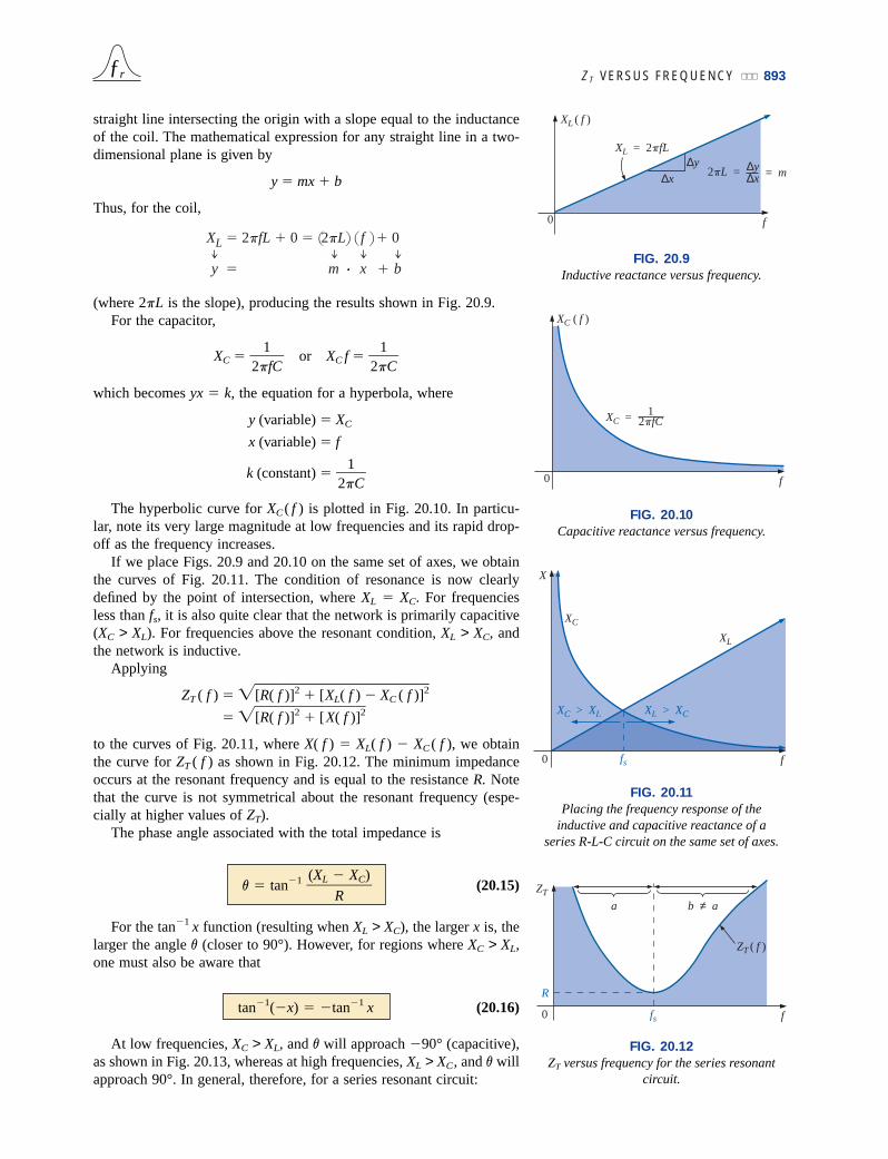
20.4 ZT VERSUS FREQUENCY
The total impedance of the series R-L-C circuit of Fig. 20.2 at any fre-quency is determined by
ZT R j XL j XC or ZT R j (XL XC)
The magnitude of the impedance ZT versus frequency is determined by
ZT R2 (XL XC)2The total-impedance-versus-frequency curve for the series resonant
circuit of Fig. 20.2 can be found by applying the impedance-versus-frequency curve for each element of the equation just derived, writtenin the following form:
(20.14)
where ZT ( f ) “means” the total impedance as a function of frequency.For the frequency range of interest, we will assume that the resistanceR does not change with frequency, resulting in the plot of Fig. 20.8. Thecurve for the inductance, as determined by the reactance equation, is a
ZT ( f ) [R( f)]2 [XL(f ) XC( f)]2
R = 6
XC = 480
–
+
E = 10 V ∠ 0°
XL = 480
FIG. 20.7
High-Q series resonant circuit.
R( f )
R
0 f
FIG. 20.8
Resistance versus frequency.
ZT VERSUS FREQUENCY 893
straight line intersecting the origin with a slope equal to the inductanceof the coil. The mathematical expression for any straight line in a two-dimensional plane is given by
y mx b
Thus, for the coil,
(where 2pL is the slope), producing the results shown in Fig. 20.9.For the capacitor,
XC or XC f
which becomes yx k, the equation for a hyperbola, where
y (variable) XC
x (variable) f
k (constant)
The hyperbolic curve for XC ( f ) is plotted in Fig. 20.10. In particu-lar, note its very large magnitude at low frequencies and its rapid drop-off as the frequency increases.
If we place Figs. 20.9 and 20.10 on the same set of axes, we obtainthe curves of Fig. 20.11. The condition of resonance is now clearlydefined by the point of intersection, where XL XC. For frequenciesless than fs, it is also quite clear that the network is primarily capacitive(XC > XL). For frequencies above the resonant condition, XL > XC, andthe network is inductive.
Applying
ZT ( f ) [R(f )]2 [XL(f ) XC(f )]2 [R(f )]2 [X(f )]2
to the curves of Fig. 20.11, where X( f ) XL( f ) XC ( f ), we obtainthe curve for ZT ( f ) as shown in Fig. 20.12. The minimum impedanceoccurs at the resonant frequency and is equal to the resistance R. Notethat the curve is not symmetrical about the resonant frequency (espe-cially at higher values of ZT).
The phase angle associated with the total impedance is
(20.15)
For the tan1 x function (resulting when XL > XC), the larger x is, thelarger the angle v (closer to 90°). However, for regions where XC > XL,one must also be aware that
(20.16)
At low frequencies, XC > XL, and v will approach 90° (capacitive),as shown in Fig. 20.13, whereas at high frequencies, XL > XC, and v willapproach 90°. In general, therefore, for a series resonant circuit:
tan1(x) tan1 x
v tan1 (XL
R
XC)
12pC
12pC
12pfC
XL 2pfL 0 2pL f 0
y m x b
ƒr
XL = 2pfL
XL ( f )
0
∆x
∆y2pL = = m∆y
∆x
f
FIG. 20.9
Inductive reactance versus frequency.
XC = 12pfC
f0
XC ( f )
FIG. 20.10
Capacitive reactance versus frequency.
XC
X
XL
XC > XL XL > XC
fs f0
FIG. 20.11
Placing the frequency response of the inductive and capacitive reactance of a
series R-L-C circuit on the same set of axes.
b ≠ a
ZT ( f )
ffs
a
ZT
R
0
FIG. 20.12
ZT versus frequency for the series resonant circuit.

894 RESONANCE
f < fs: network capacitive; I leads Ef > fs: network inductive; E leads If fs: network resistive; E and I are in phase
ƒr
Circuit capacitiveLeading Fp
v
90°45°0°
–45°–90°
(E leads I)
Circuit inductiveLagging Fp
fs f
FIG. 20.13
Phase plot for the series resonant circuit.
20.5 SELECTIVITY
If we now plot the magnitude of the current I E/ZT versus frequencyfor a fixed applied voltage E, we obtain the curve shown in Fig. 20.14,which rises from zero to a maximum value of E/R (where ZT is a mini-mum) and then drops toward zero (as ZT increases) at a slower rate thanit rose to its peak value. The curve is actually the inverse of the imped-ance-versus-frequency curve. Since the ZT curve is not absolutely sym-metrical about the resonant frequency, the curve of the current versusfrequency has the same property.
BW
I
Imax = ER
0.707Imax
0 f1 fs f2 f
FIG. 20.14
I versus frequency for the series resonant circuit.
There is a definite range of frequencies at which the current is nearits maximum value and the impedance is at a minimum. Those fre-quencies corresponding to 0.707 of the maximum current are called theband frequencies, cutoff frequencies, or half-power frequencies.They are indicated by f1 and f2 in Fig. 20.14. The range of frequenciesbetween the two is referred to as the bandwidth (abbreviated BW) ofthe resonant circuit.
Half-power frequencies are those frequencies at which the powerdelivered is one-half that delivered at the resonant frequency; that is,
(20.17)PHPF 12
Pmax

SELECTIVITY 895
The above condition is derived using the fact that
Pmax I2maxR
and PHPF I 2R (0.707Imax)2R (0.5)(I2
maxR) Pmax
Since the resonant circuit is adjusted to select a band of frequencies,the curve of Fig. 20.14 is called the selectivity curve. The term isderived from the fact that one must be selective in choosing the fre-quency to ensure that it is in the bandwidth. The smaller the bandwidth,the higher the selectivity. The shape of the curve, as shown in Fig.20.15, depends on each element of the series R-L-C circuit. If the resis-tance is made smaller with a fixed inductance and capacitance, thebandwidth decreases and the selectivity increases. Similarly, if the ratioL/C increases with fixed resistance, the bandwidth again decreases withan increase in selectivity.
In terms of Qs, if R is larger for the same XL, then Qs is less, asdetermined by the equation Qs qsL/R.
A small Qs, therefore, is associated with a resonant curve having alarge bandwidth and a small selectivity, while a large Qs indicates theopposite.
For circuits where Qs 10, a widely accepted approximation is thatthe resonant frequency bisects the bandwidth and that the resonantcurve is symmetrical about the resonant frequency.
These conditions are shown in Fig. 20.16, indicating that the cutoff fre-quencies are then equidistant from the resonant frequency.
For any Qs, the preceding is not true. The cutoff frequencies f1 and f2can be found for the general case (any Qs) by first employing the factthat a drop in current to 0.707 of its resonant value corresponds to anincrease in impedance equal to 1/0.707 2 times the resonant value,which is R.
Substituting 2R into the equation for the magnitude of ZT, we findthat
ZT R2 (XL XC)2becomes 2R R2 (XL XC)2or, squaring both sides, that
2R2 R2 (XL XC)2
and R2 (XL XC)2
Taking the square root of both sides gives us
R XL XC or R XL XC 0
Let us first consider the case where XL > XC, which relates to f2 orq2. Substituting q2L for XL and 1/q2C for XC and bringing both quanti-ties to the left of the equal sign, we have
R q2L 0 or Rq2 q22L 0
which can be written
q22 q2 0
1LC
RL
1C
1q2C
12
ƒr
BW
BW
fs f0
IR3 > R2 > R1 (L, C fixed)
R1(smaller)
R2
R3(larger)
fs f0
I
BW2
BW3
BW1
L3 /C3
L2/C2
L1/C1
(R fixed)L3/C3 > L2/C2 > L1/C1
(a)
(b)
BW
FIG. 20.15
Effect of R, L, and C on the selectivity curve for the series resonant circuit.
Imax
0.707Imax
a
b
a = b
f1 f2fs
FIG. 20.16
Approximate series resonance curve for Qs ≥ 10.
896 RESONANCE
Solving the quadratic, we have
q2
and q2 RL2
2
L4
C
with f2 21p
2RL
12
RL
2
L4
C (Hz) (20.18)
The negative sign in front of the second factor was dropped because
(1/2)(R/L)2 4/LC is always greater than R/(2L). If it were notdropped, there would be a negative solution for the radian frequency q.
If we repeat the same procedure for XC > XL, which relates to q1 or
f1 such that ZT R2 (XC XL)2, the solution f1 becomes
f1 21p
2RL
12
RL
2
L4
C (Hz) (20.19)
The bandwidth (BW) is
BW f2 f1 Eq. (20.18) Eq. (20.19)
and (20.20)
Substituting R/L qs /Qs from Qs qsL /R and 1/2p fs /qs from qs 2pfs gives us
BW
or (20.21)
which is a very convenient form since it relates the bandwidth to the Qs
of the circuit. As mentioned earlier, Equation (20.21) verifies that thelarger the Qs, the smaller the bandwidth, and vice versa.
Written in a slightly different form, Equation (20.21) becomes
(20.22)
The ratio ( f2 f1)/fs is sometimes called the fractional bandwidth, pro-viding an indication of the width of the bandwidth compared to the res-onant frequency.
It can also be shown through mathematical manipulations of the per-tinent equations that the resonant frequency is related to the geometricmean of the band frequencies; that is,
f2
fs
f1
Q
1
s
BW Q
fs
s
qsQs
fsqs
RL
12p
R2pL
BW f2 f1 2p
RL
12
R2L
(R/L) [(R/L)]2 [(4/LC)]
2
ƒr

VR, VL, AND VC 897
(20.23)
20.6 VR, VL, AND VC
Plotting the magnitude (effective value) of the voltages VR, VL, and VC
and the current I versus frequency for the series resonant circuit on thesame set of axes, we obtain the curves shown in Fig. 20.17. Note thatthe VR curve has the same shape as the I curve and a peak value equalto the magnitude of the input voltage E. The VC curve builds up slowlyat first from a value equal to the input voltage since the reactance of thecapacitor is infinite (open circuit) at zero frequency and the reactance ofthe inductor is zero (short circuit) at this frequency. As the frequencyincreases, 1/qC of the equation
VC IXC (I ) 1qC
fs f1f2
ƒr
VL
VCmax = VLmax
VCs = VLs
= QE
VRI
ffLmax
fCmax
fs0
Imax
E
VC
FIG. 20.17
VR, VL, VC, and I versus frequency for a series resonant circuit.
becomes smaller, but I increases at a rate faster than that at which 1/qCdrops. Therefore, VC rises and will continue to rise due to the quicklyrising current, until the frequency nears resonance. As it approaches theresonant condition, the rate of change of I decreases. When this occurs,the factor 1/qC, which decreased as the frequency rose, will overcomethe rate of change of I, and VC will start to drop. The peak value willoccur at a frequency just before resonance. After resonance, both VC
and I drop in magnitude, and VC approaches zero.The higher the Qs of the circuit, the closer fCmax
will be to fs, and thecloser VCmax
will be to QsE. For circuits with Qs ≥ 10, fCmax fs, and
VCmax QsE.
The curve for VL increases steadily from zero to the resonant fre-quency since both quantities qL and I of the equation VL IXL (I)(qL) increase over this frequency range. At resonance, I has reachedits maximum value, but qL is still rising. Therefore, VL will reach itsmaximum value after resonance. After reaching its peak value, the volt-age VL will drop toward E since the drop in I will overcome the rise inqL. It approaches E because XL will eventually be infinite, and XC willbe zero.

898 RESONANCE
As Qs of the circuit increases, the frequency fLmaxdrops toward fs, and
VLmaxapproaches QsE. For circuits with Qs ≥ 10, fLmax
fs, and VLmax
QsE.The VL curve has a greater magnitude than the VC curve for any fre-
quency above resonance, and the VC curve has a greater magnitude thanthe VL curve for any frequency below resonance. This again verifies thatthe series R-L-C circuit is predominantly capacitive from zero to theresonant frequency and predominantly inductive for any frequencyabove resonance.
For the condition Qs ≥ 10, the curves of Fig. 20.17 will appear asshown in Fig. 20.18. Note that they each peak (on an approximatebasis) at the resonant frequency and have a similar shape.
ƒr
VCmax = VLmax
= QsE
VC
EVL
VRImax
0 f1 fs f2
I
VL
VC
f
FIG. 20.18
VR, VL, VC, and I for a series resonant circuit where Qs ≥ 10.
In review,
1. VC and VL are at their maximum values at or near resonance(depending on Qs).
2. At very low frequencies, VC is very close to the source voltageand VL is very close to zero volts, whereas at very high frequen-cies, VL approaches the source voltage and VC approaches zerovolts.
3. Both VR and I peak at the resonant frequency and have the sameshape.
20.7 EXAMPLES (SERIES RESONANCE)
EXAMPLE 20.1
a. For the series resonant circuit of Fig. 20.19, find I, VR, VL, and VC
at resonance.b. What is the Qs of the circuit?c. If the resonant frequency is 5000 Hz, find the bandwidth.d. What is the power dissipated in the circuit at the half-power fre-
quencies?
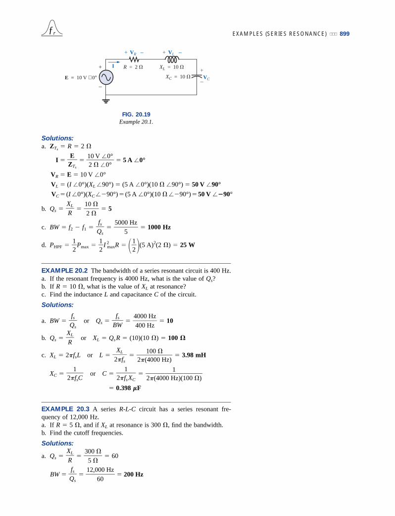
EXAMPLES (SERIES RESONANCE) 899
Solutions:
a. ZTs R 2
I 5 A 0°
VR E 10 V 0°
VL (I 0°)(XL 90°) (5 A 0°)(10 90°) 50 V 90°
10 V 0°2 0°
EZTs
ƒr
VR
VC
–
+
E = 10 V ∠ 0°
I
+ –
R = 2 XL = 10
VL+ –
XC = 10 +
–
FIG. 20.19
Example 20.1.
VC (I 0°)(XC 90°) (5 A 0°)(10 90°)50 V 90°
b. Qs 5
c. BW f2 f1 1000 Hz5000 Hz
5
fsQs
10 2
XLR
d. PHPF Pmax I 2maxR (5 A)2(2 ) 25 W
EXAMPLE 20.2 The bandwidth of a series resonant circuit is 400 Hz.a. If the resonant frequency is 4000 Hz, what is the value of Qs?b. If R 10 , what is the value of XL at resonance?c. Find the inductance L and capacitance C of the circuit.
Solutions:
a. BW or Qs 10
b. Qs or XL QsR (10)(10 ) 100
c. XL 2pfsL or L 3.98 mH
XC or C
0.398 mF
EXAMPLE 20.3 A series R-L-C circuit has a series resonant fre-quency of 12,000 Hz.a. If R 5 , and if XL at resonance is 300 , find the bandwidth.b. Find the cutoff frequencies.
Solutions:
a. Qs 60
BW 200 Hz12,000 Hz
60
fsQs
300
5
XLR
12p(4000 Hz)(100 )
12pfsXC
12pfsC
100 2p(4000 Hz)
XL2pfs
XLR
4000 Hz400 Hz
fsBW
fsQs
12
12
12

900 RESONANCE
b. Since Qs ≥ 10, the bandwidth is bisected by fs. Therefore,
f2 fs 12,000 Hz 100 Hz 12,100 Hz
and f1 12,000 Hz 100 Hz 11,900 Hz
EXAMPLE 20.4
a. Determine the Qs and bandwidth for the response curve of Fig.20.20.
b. For C 101.5 nF, determine L and R for the series resonant circuit.c. Determine the applied voltage.
Solutions:
a. The resonant frequency is 2800 Hz. At 0.707 times the peak value,
BW 200 Hz
and Qs 14
b. fs or L
31.832 mH
Qs or R
40
c. Imax or E ImaxR
(200 mA)(40 ) 8 V
EXAMPLE 20.5 A series R-L-C circuit is designed to resonant at qs 105 rad/s, have a bandwidth of 0.15qs, and draw 16 W from a 120-Vsource at resonance.a. Determine the value of R.b. Find the bandwidth in hertz.c. Find the nameplate values of L and C.d. Determine the Qs of the circuit.e. Determine the fractional bandwidth.
Solutions:
a. P and R 900
b. fs 15,915.49 Hz
BW 0.15fs 0.15(15,915.49 Hz) 2387.32 Hz
c. Eq. (20.20):
BW and L 60 mH900
2p(2387.32 Hz)
R2pBW
R2pL
105 rad/s
2p
qs2p
(120 V)2
16 W
E2
P
E2
R
ER
2p(2800 Hz)(31.832 103 H)
14
XLQs
XLR
14p2(2.8 103 Hz)2(101.5 109 F)
14p2fs
2C1
2pLC
2800 Hz200 Hz
fsBW
BW
2
ƒr
I (mA)
200
100
0 2000 3000 4000 f (Hz)
FIG. 20.20
Example 20.4.
fs and C
1.67 nF
14p2(15,915.49 Hz)2(60 103 H)
14p2fs
2L
12pLC
PARALLEL RESONANT CIRCUIT 901
d. Qs 6.67
e. 0.15
PARALLEL RESONANCE
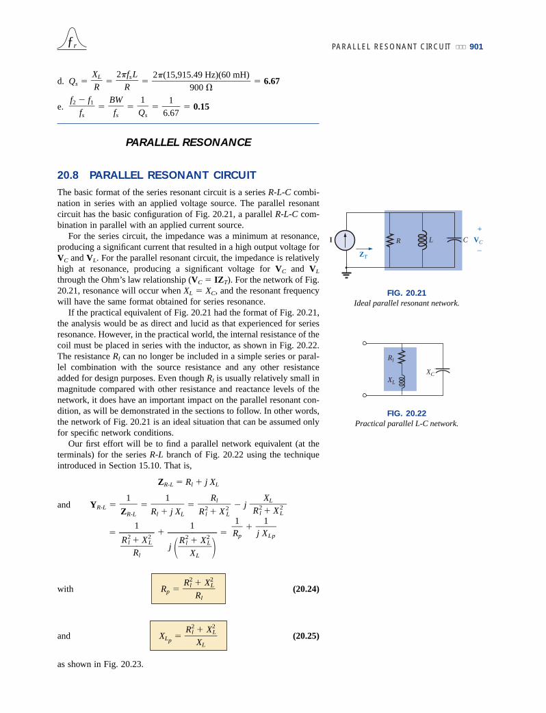
20.8 PARALLEL RESONANT CIRCUIT
The basic format of the series resonant circuit is a series R-L-C combi-nation in series with an applied voltage source. The parallel resonantcircuit has the basic configuration of Fig. 20.21, a parallel R-L-C com-bination in parallel with an applied current source.
For the series circuit, the impedance was a minimum at resonance,producing a significant current that resulted in a high output voltage forVC and VL. For the parallel resonant circuit, the impedance is relativelyhigh at resonance, producing a significant voltage for VC and VL
through the Ohm’s law relationship (VC IZT). For the network of Fig.20.21, resonance will occur when XL XC, and the resonant frequencywill have the same format obtained for series resonance.
If the practical equivalent of Fig. 20.21 had the format of Fig. 20.21,the analysis would be as direct and lucid as that experienced for seriesresonance. However, in the practical world, the internal resistance of thecoil must be placed in series with the inductor, as shown in Fig. 20.22.The resistance Rl can no longer be included in a simple series or paral-lel combination with the source resistance and any other resistanceadded for design purposes. Even though Rl is usually relatively small inmagnitude compared with other resistance and reactance levels of thenetwork, it does have an important impact on the parallel resonant con-dition, as will be demonstrated in the sections to follow. In other words,the network of Fig. 20.21 is an ideal situation that can be assumed onlyfor specific network conditions.
Our first effort will be to find a parallel network equivalent (at theterminals) for the series R-L branch of Fig. 20.22 using the techniqueintroduced in Section 15.10. That is,
ZR-L Rl j XL
and YR-L j
with (20.24)
and (20.25)
as shown in Fig. 20.23.
XLp
R2l
XL
X2L
Rp R2
l
Rl
X2L
1——
j R2l
X
L
X2L
1
—
R2
l
Rl
X2L
XLR2
l X2L
RlR2
l X2L
1Rl j XL
1ZR-L
16.67
1Qs
BW
fs
f2 f1
fs
2p(15,915.49 Hz)(60 mH)
900
2pfsL
R
XLR
ƒr
C VC
+
–R L
ZT
I
FIG. 20.21
Ideal parallel resonant network.
Rl
XL
XC
FIG. 20.22
Practical parallel L-C network.
R1
p
j X1
Lp

902 RESONANCE
Redrawing the network of Fig. 20.22 with the equivalent of Fig.20.23 and a practical current source having an internal resistance Rs willresult in the network of Fig. 20.24.
ƒr
Rl
XL
RpRl
2 + XL2
RLXLp
Rl2 + XL
2
RL=
FIG. 20.23
Equivalent parallel network for a series R-L combination.
I Rp
+VpXLp
–XCRs
ZT
YT
Source
FIG. 20.24
Substituting the equivalent parallel network for the series R-L combination ofFig. 20.22.
If we define the parallel combination of Rs and Rp by the notation
(20.26)
the network of Fig. 20.25 will result. It has the same format as the idealconfiguration of Fig. 20.21.
We are now at a point where we can define the resonance condi-tions for the practical parallel resonant configuration. Recall that forseries resonance, the resonant frequency was the frequency at whichthe impedance was a minimum, the current a maximum, and the inputimpedance purely resistive, and the network had a unity power factor.For parallel networks, since the resistance Rp in our equivalent modelis frequency dependent, the frequency at which maximum VC isobtained is not the same as required for the unity-power-factor char-acteristic. Since both conditions are often used to define the resonantstate, the frequency at which each occurs will be designated by differ-ent subscripts.
Unity Power Factor, fp
For the network of Fig. 20.25,
YT
j j 1XC
1XLp
1R
1j XC
1j XLp
1R
1Z3
1Z2
1Z1
R Rs Rp
XCR XLp
YT
I
ZT
FIG. 20.25
Substituting R Rs Rp for the network ofFig. 20.24.

PARALLEL RESONANT CIRCUIT 903
and (20.27)
For unity power factor, the reactive component must be zero asdefined by
0
Therefore,
and (20.28)
Substituting for XLpyields
(20.29)
The resonant frequency, fp, can now be determined from Eq. (20.29) asfollows:
R2l X2
L XC XL qL
or X2L R2
l
with 2pfpL R2l
and fp R2l
Multiplying the top and bottom of the factor within the square-rootsign by C/L produces
fp 1
and fp 1 RL
2l C (20.30)
or fp fs1 RL
2l C (20.31)
where fp is the resonant frequency of a parallel resonant circuit (for Fp 1) and fs is the resonant frequency as determined by XL XC forseries resonance. Note that unlike a series resonant circuit, the resonant
12pLC
R2lC
L
12pLC/L
1 R2l(C/L)
C/L
12pL
LC
12pL
LC
LC
LC
1qC
R2
l
XL
X2L
XC
XLp XC
1XLp
1XC
1XLp
1XC
YT R
1 j
X
1
C
X
1
Lp
ƒr

904 RESONANCE
frequency fp is a function of resistance (in this case Rl). Note also, how-ever, the absence of the source resistance Rs in Eqs. (20.30) and (20.31).Since the factor 1 (R2
lC/L) is less than 1, fp is less than fs. Recog-nize also that as the magnitude of Rl approaches zero, fp rapidlyapproaches fs.
Maximum Impedance, fm
At f fp the input impedance of a parallel resonant circuit will benear its maximum value but not quite its maximum value due to thefrequency dependence of Rp. The frequency at which maximumimpedance will occur is defined by fm and is slightly more than fp, asdemonstrated in Fig. 20.26. The frequency fm is determined by differ-entiating (calculus) the general equation for ZT with respect to fre-quency and then determining the frequency at which the resultingequation is equal to zero. The algebra is quite extensive and cumber-some and will not be included here. The resulting equation, however,is the following:
fm fs1 (20.32)
Note the similarities with Eq. (20.31). Since the square-root factor ofEq. (20.32) is always more than the similar factor of Eq. (20.31), fm isalways closer to fs and more than fp. In general,
(20.33)
Once fm is determined, the network of Fig. 20.25 can be used todetermine the magnitude and phase angle of the total impedance at theresonance condition simply by substituting f fm and performing therequired calculations. That is,
f fm(20.34)
20.9 SELECTIVITY CURVE FORPARALLEL RESONANT CIRCUITS
The ZT -versus-frequency curve of Fig. 20.26 clearly reveals that a par-allel resonant circuit exhibits maximum impedance at resonance ( fm),unlike the series resonant circuit, which experiences minimum resis-tance levels at resonance. Note also that ZT is approximately Rl at f 0 Hz since ZT Rs Rl Rl.
Since the current I of the current source is constant for any value ofZT or frequency, the voltage across the parallel circuit will have thesame shape as the total impedance ZT, as shown in Fig. 20.27.
For the parallel circuit, the resonance curve of interest is that of thevoltage VC across the capacitor. The reason for this interest in VC
derives from electronic considerations that often place the capacitor atthe input to another stage of a network.
ZTm R XLp
XC
fs > fm > fp
R2lC
L
14
ƒr
FIG. 20.26
ZT versus frequency for the parallel resonant circuit.
ZT
ZTm
Rl0 fm f
Vp( f ) I( f ) ZT ( f )
FIG. 20.27
Defining the shape of the Vp(f) curve.

SELECTIVITY CURVE FOR PARALLEL RESONANT CIRCUITS 905
Since the voltage across parallel elements is the same,
(20.35)
The resonant value of VC is therefore determined by the value of ZTm
and the magnitude of the current source I.The quality factor of the parallel resonant circuit continues to be
determined by the ratio of the reactive power to the real power. That is,
Qp
where R Rs Rp, and Vp is the voltage across the parallel branches.The result is
Qp X
R
Lp
(20.36a)
or since XLp XC at resonance,
Qp (20.36b)
For the ideal current source (Rs ∞ ) or when Rs is sufficientlylarge compared to Rp, we can make the following approximation:
R Rs Rp Rp
and Qp
so that Qp X
RL
l Ql
Rs k Rp
(20.37)
which is simply the quality factor Ql of the coil.In general, the bandwidth is still related to the resonant frequency
and the quality factor by
BW f2 f1 Q
fr
p (20.38)
The cutoff frequencies f1 and f2 can be determined using the equiva-lent network of Fig. 20.25 and the unity power condition for resonance.The half-power frequencies are defined by the condition that the outputvoltage is 0.707 times the maximum value. However, for parallel reso-nance with a current source driving the network, the frequency responsefor the driving point impedance is the same as that for the output volt-age. This similarity permits defining each cutoff frequency as the fre-quency at which the input impedance is 0.707 times its maximumvalue. Since the maximum value is the equivalent resistance R of Fig.20.25, the cutoff frequencies will be associated with an impedanceequal to 0.707R or (1/2)R.
(R2l X2
L)/Rl(R2
l X2L)/XL
RpXLp
Rs Rp
XLp
Rs Rp
XC
Rs Rp
XLp
V2p /XLp
V2
p /R
VC Vp IZT
ƒr
906 RESONANCE
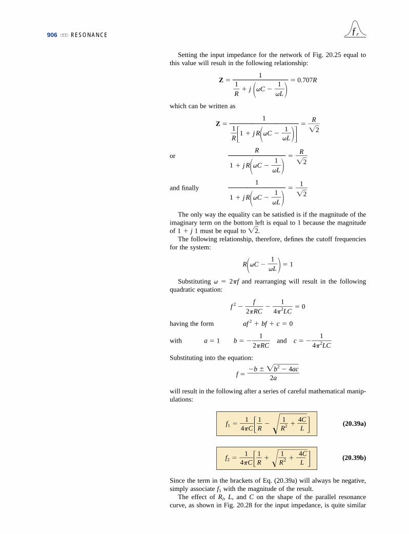
Setting the input impedance for the network of Fig. 20.25 equal tothis value will result in the following relationship:
Z 0.707R
which can be written as
Z R
2
1———
R
11 j RqC
q
1L
1———R
1 j qC
q
1
L
ƒr
or
and finally
The only way the equality can be satisfied is if the magnitude of theimaginary term on the bottom left is equal to 1 because the magnitudeof 1 j 1 must be equal to 2.
The following relationship, therefore, defines the cutoff frequenciesfor the system:
RqC 1
Substituting q 2pf and rearranging will result in the followingquadratic equation:
f 2 0
having the form af 2 bf c 0
with a 1 b and c
Substituting into the equation:
f
will result in the following after a series of careful mathematical manip-ulations:
f1 4p
1C
R1
R12
4LC (20.39a)
f2 4p
1C
R1
R12 4
LC (20.39b)
Since the term in the brackets of Eq. (20.39a) will always be negative,simply associate f1 with the magnitude of the result.
The effect of Rl, L, and C on the shape of the parallel resonancecurve, as shown in Fig. 20.28 for the input impedance, is quite similar
b b2 4ac
2a
14p2LC
12pRC
14p2LC
f2pRC
1qL
12
1———
1 j RqC q
1
L
R2
R———
1 j RqC q
1
L

EFFECT OF Ql ≥ 10 907
to their effect on the series resonance curve. Whether or not Rl is zero,the parallel resonant circuit will frequently appear in a networkschematic as shown in Fig. 20.28.
At resonance, an increase in Rl or a decrease in the ratio L /C willresult in a decrease in the resonant impedance, with a correspondingincrease in the current. The bandwidth of the resonance curves is givenby Eq. (20.38). For increasing Rl or decreasing L (or L /C for constantC), the bandwidth will increase as shown in Fig. 20.28.
At low frequencies, the capacitive reactance is quite high, and theinductive reactance is low. Since the elements are in parallel, the totalimpedance at low frequencies will therefore be inductive. At high fre-quencies, the reverse is true, and the network is capacitive. At reso-nance ( fp), the network appears resistive. These facts lead to the phaseplot of Fig. 20.29. Note that it is the inverse of that appearing for theseries resonant circuit because at low frequencies the series resonantcircuit was capacitive and at high frequencies it was inductive.
ƒr
Rl3
ffr0
Rl3 > Rl2
> Rl1
L/C fixed
ZpRl1
Rl2
Rl
ffr0
ZpL3
C3
L2
C2
L1
C1> >
Rl fixed L3/C3
L2/C2
L1/C1
FIG. 20.28
Effect of Rl, L, and C on the parallel resonance curve.
20.10 EFFECT OF Ql ≥ 10
The content of the previous section may suggest that the analysis ofparallel resonant circuits is significantly more complex than encoun-tered for series resonant circuits. Fortunately, however, this is not thecase since, for the majority of parallel resonant circuits, the quality fac-tor of the coil Ql is sufficiently large to permit a number of approxima-tions that simplify the required analysis.
FIG. 20.29
Phase plot for the parallel resonant circuit.
Resonance (resistive)Circuit inductiveLagging Fp
Circuit capacitiveLeading Fp
fp f
θ (Vp leads I)
90°
45°
0°
–45°
–90°

908 RESONANCE
Inductive Reactance, XLp
If we expand XLpas
XLp XL XL
then, for Ql ≥ 10, XL /Q2l 0 compared to XL, and
Ql ≥ 10(20.40)
and since resonance is defined by XLp XC, the resulting condition for
resonance is reduced to:
Ql ≥ 10(20.41)
Resonant Frequency, fp (Unity Power Factor)
We can rewrite the factor R2lC/L of Eq. (20.31) as
and substitute Eq. (20.41) (XL XC):
Equation (20.31) then becomes
fp fs1 Q1
2l
Ql ≥ 10
(20.42)
clearly revealing that as Ql increases, fp becomes closer and closer to fs.For Ql ≥ 10,
1 1
and fp fs Ql ≥ 10
(20.43)
Resonant Frequency, fm (Maximum VC)
Using the equivalency R2lC/L 1/Q2
l derived for Eq. (20.42), Equation(20.32) will take on the following form:
fm fs1 Ql ≥ 10
(20.44)1
Q2
l
14
12pLC
1Q2
l
1Q2
l
1—
X
R
2L
2l
1—
XL
R
X2l
C
1—X
RLX
2l
C
1—R
q2l q
L
C
1—(
(
q
q
)
)
R
L2l C
1—R
L2l C
R2lC
L
XL XC
XLp XL
XLQ2
l
R2l(XL)
XL(XL)
R2l X2
L
XL
ƒr

EFFECT OF Ql ≥ 10 909
The fact that the negative term under the square root will always beless than that appearing in the equation for fp reveals that fm will alwaysbe closer to fs than fp.
For Ql ≥ 10 the negative term becomes very small and can bedropped from consideration, leaving:
fm fs 2p
1
LC
Ql ≥ 10
(20.45)
In total, therefore, for Ql ≥ 10,
Ql ≥ 10 (20.46)
Rp
Rp Rl Rl Rl
Rl Q2l Rl (1 Q2
l )Rl
For Ql ≥ 10, 1 Q2l Q2
l , and
Ql ≥ 10(20.47)
Applying the approximations just derived to the network of Fig.20.24 will result in the approximate equivalent network for Ql ≥ 10 ofFig. 20.30, which is certainly a lot “cleaner” in general appearance.
Rp Q2lRl
X2L
R2
l
RlRl
X2L
Rl
R2l X2
L
Rl
fp fm fs
ƒr
Rs Rp = Q2RlZTp
I XLp = XL XC
FIG. 20.30
Approximate equivalent circuit for Ql ≥ 10.
Substituting Ql into Eq. (20.47),
Rp Ql2Rl
2Rl
andQl ≥ 10
(20.48)
ZTp
The total impedance at resonance is now defined by
Ql ≥ 10(20.49)ZTp
Rs Rp Rs Q2lRl
Rp R
L
lC
2pfLRl(2pfC)
XLXC
Rl
XL2
Rl
XLRl
XLRl

910 RESONANCE
For an ideal current source (Rs ∞ ), or if Rs k Rp, the equationreduces to
Ql ≥ 10, Rs k Rp
(20.50)
Qp
The quality factor is now defined by
Qp (20.51)
Quite obviously, therefore, Rs does have an impact on the qualityfactor of the network and the shape of the resonant curves.
If an ideal current source (Rs ∞ ) is employed, or if Rs k Rp,
Qp
and Ql ≥ 10, Rs k Rp(20.52)
BW
The bandwidth defined by fp is
BW f2 f1 Q
fp
p (20.53)
By substituting Qp from above and performing a few algebraic manip-ulations, we can show that
BW f2 f1 (20.54)
clearly revealing the impact of Rs on the resulting bandwidth. Of course,if Rs ∞ (ideal current source):
BW f2 f1 2
R
p
l
L
Rs ∞
(20.55)
IL and IC
A portion of Fig. 20.30 is reproduced in Fig. 20.31, with IT defined asshown.
As indicated, ZTpat resonance is Q2
lR
l. The voltage across the paral-
lel network is, therefore,
VC VL VR ITZTp IT Q2
lRl
1RsC
RlL
12p
Qp Ql
Q2l
Ql
Q2l
XL/Rl
Q2lRl
XL
Rs Q2lRl
XL
Rs Q2l Rl
XL
RXLp
ZTp Q2
lRl
ƒr

SUMMARY TABLE 911
The magnitude of the current IC can then be determined using Ohm’slaw, as follows:
IC
Substituting XC XL when Ql ≥ 10,
IC IT IT
and Ql ≥ 10 (20.56)
revealing that the capacitive current is Ql times the magnitude of thecurrent entering the parallel resonant circuit. For large Ql, the current IC
can be significant.A similar derivation results in
Ql ≥ 10 (20.57)
Conclusions
The equations resulting from the application of the condition Ql ≥ 10are obviously a great deal easier to apply than those obtained earlier. Itis, therefore, a condition that should be checked early in an analysis todetermine which approach must be applied. Although the condition Ql ≥ 10 was applied throughout, many of the equations are still goodapproximations for Ql < 10. For instance, if Ql 5, XLp
(XL/Q2l )
Xl (XL/25) XL 1.04XL, which is very close to XL. In fact, forQl 2, XLp
(XL/4) XL 1.25XL, which agreeably is not XL, but itis only 25% off. In general, be aware that the approximate equationscan be applied with good accuracy with Ql < 10. The smaller the levelof Ql, however, the less valid the approximation. The approximate equa-tions are certainly valid for a range of values of Ql < 10 if a roughapproximation to the actual response is desired rather than one accurateto the hundredths place.
20.11 SUMMARY TABLE
In an effort to limit any confusion resulting from the introduction of fpand fm and an approximate approach dependent on Ql, summary Table20.1 was developed. One can always use the equations for any Ql, but
IL QlIT
IC QlIT
Q2l
Ql
Q2l
—
X
RL
l
IT Q2lRl
XL
ITQ2lRl
XC
VCXC
ƒr
IT
RP XL XC VC
+
–
ICIL
ZTp = Rp = Ql
2Rl
FIG. 20.31
Establishing the relationship between IC and IL and the current IT.

912 RESONANCE ƒr
a proficiency in applying the approximate equations defined by Ql willpay dividends in the long run.
For the future, the analysis of a parallel resonant network might pro-ceed as follows:
1. Determine fs to obtain some idea of the resonant frequency.Recall that for most situations, fs, fm, and fp will be relativelyclose to each other.
2. Calculate an approximate Ql using fs from above, and compare itto the condition Ql ≥ 10. If the condition is satisfied, the approx-imate approach should be the chosen path unless a high degree ofaccuracy is required.
3. If Ql is less than 10, the approximate approach can be applied, butit must be understood that the smaller the level of Ql, the lessaccurate the solution. However, considering the typical variationsfrom nameplate values for many of our components and that aresonant frequency to the tenths place is seldom required, the useof the approximate approach for many practical situations is usu-ally quite valid.
20.12 EXAMPLES (PARALLEL RESONANCE)
EXAMPLE 20.6 Given the parallel network of Fig. 20.32 composedof “ideal” elements:a. Determine the resonant frequency fp.b. Find the total impedance at resonance.c. Calculate the quality factor, bandwidth, and cutoff frequencies f1 and
f2 of the system.
TABLE 20.1
Parallel resonant circuit (fs 1/(2pLC)).
Any Ql Ql ≥ 10 Ql ≥ 10, Rs k Ql2Rl
fp fs1 fs fs
fm fs1 fs fs
ZTpRs Rp Rs Rs Q2
lRl Q2lRl
ZTmRs ZRL ZC Rs Q2
l Rl Q2lRl
Qp Ql
BW or
IL , IC Network analysis IL IC QlIT IL IC QlIT
fsQl
fpQl
fsQp
fpQp
fmQp
fpQp
ZTpXC
ZTpXL
ZTpXC
ZTpXLp
R2l X2
L
Rl
R2lC
L
14
R2lC
L

EXAMPLES (PARALLEL RESONANCE) 913
d. Find the voltage VC at resonance.e. Determine the currents IL and IC at resonance.
Solutions:
a. The fact that Rl is zero ohms results in a very high Ql ( XL/Rl), per-mitting the use of the following equation for fp:
fp fs
5.03 kHz
b. For the parallel reactive elements:
ZL ZC
but XL XC at resonance, resulting in a zero in the denominator ofthe equation and a very high impedance that can be approximated byan open circuit. Therefore,
ZTp Rs ZL ZC Rs 10 k
c. Qp 316.41
BW 15.90 Hz
Eq. (20.39a):
f1 R
12 4L
C1
R
14pC
5.03 kHz
316.41
fpQp
10 k2p(5.03 kHz)(1 mH)
Rs2pfpL
RsXLp
(XL 90°)(XC 90°)
j(XL XC)
12p(1 mH)(1mF)
12pLC
ƒr
FIG. 20.32
Example 20.6.
ZTp10 k 1 mH 1 mF VC
+
–
ICIL
I = 10 mA Rs
Source “Tank circuit”
L C
5.025 kHz
Eq. (20.39b):
f2 4p
1
C
R
1
R
12 4L
C
5.041 kHz
d. VC IZTp (10 mA)(10 k) 100 V
e. IL 3.16 A
IC 3.16 A ( QpI )100 V31.6
VCXC
100 V31.6
100 V2p(5.03 kHz)(1 mH)
VC2pfp L
VLXL
4(1 mF)
1 mH1
(10 k)2
110 k
14p(1 mF)
914 RESONANCE
Example 20.6 demonstrates the impact of Rs on the calculationsassociated with parallel resonance. The source impedance is the onlyfactor to limit the input impedance and the level of VC.
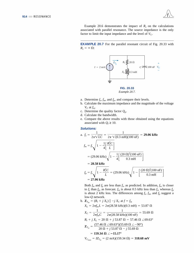
EXAMPLE 20.7 For the parallel resonant circuit of Fig. 20.33 with Rs :
ƒr
Rl 20
XL 0.3 mH
C 100 nF VC
+
–
ZTp
I = 2 mA
a. Determine fs, fm, and fp, and compare their levels.b. Calculate the maximum impedance and the magnitude of the voltage
VC at fm.c. Determine the quality factor Qp.d. Calculate the bandwidth.e. Compare the above results with those obtained using the equations
associated with Ql ≥ 10.
Solutions:
a. fs 29.06 kHz1
2p (0.3 mH)(100 nF)
12pLC
FIG. 20.33
Example 20.7.
fm fs1 1
4RL
2lC
(29.06 kHz)1 28.58 kHz
fp fs1 RL
2lC (29.06 kHz)1
27.06 kHz
Both fm and fp are less than fs, as predicted. In addition, fm is closerto fs than fp, as forecast. fm is about 0.5 kHz less than fs, whereas fpis about 2 kHz less. The differences among fs, fm, and fp suggest alow-Q network.
b. ZTm (Rl j XL) j XC at f fm
XL 2pfmL 2p(28.58 kHz)(0.3 mH) 53.87
XC 55.69
Rl j XL 20 j 53.87 57.46 69.63°
ZTm
159.34 15.17°
VCmax IZTm
(2 mA)(159.34 ) 318.68 mV
(57.46 69.63°)(55.69 90°)
20 j 53.87 j 55.69
12p(28.58 kHz)(100 nF)
12pfmC
(20 )2(100 nF)
0.3 mH
(20 )2(100 nF)
0.3 mH
14

EXAMPLES (PARALLEL RESONANCE) 915
c. Rs ∞ ; therefore,
Qp Ql
2.55
The low Q confirms our conclusion of part (a). The differencesamong fs, fm, and fp will be significantly less for higher-Q net-works.
d. BW 10.61 kHz
e. For Ql ≥ 10, fm fp fs 29.06 kHz
Qp Ql 2.74
(versus 2.55 above)
ZTp Q2
lRl (2.74)2• 20 150.15 0°
(versus 159.34 15.17° above)
VCmax IZTp
(2 mA)(150.15 ) 300.3 mV(versus 318.68 mV above)
BW 10.61 kHz
(versus 10.61 kHz above)
The results reveal that, even for a relatively low Q system, the approx-imate solutions are still in the ballpark compared to those obtainedusing the full equations. The primary difference is between fs and fp(about 7%), with the difference between fs and fm at less than 2%. Forthe future, using fs to determine Ql will certainly provide a measure ofQl that can be used to determine whether the approximate approach isappropriate.
EXAMPLE 20.8 For the network of Fig. 20.34 with fp provided:a. Determine Ql.b. Determine Rp.c. Calculate ZTp.
d. Find C at resonance.e. Find Qp.f. Calculate the BW and cutoff frequencies.
Solutions:
a. Ql 25.12
b. Ql ≥ 10. Therefore,
Rp Q2lRl (25.12)2(10 ) 6.31 k
c. ZTp Rs Rp 40 k 6.31 k 5.45 k
d. Ql ≥ 10. Therefore,
fp
and C 15.83 nF1
4p2(0.04 MHz)2(1 mH)
14p2f 2L
12pLC
2p(0.04 MHz)(1 mH)
10
2pfpL
Rl
XLRl
29.06 kHz
2.74
fpQp
2p(29.06 kHz)(0.3 mH)
20
2pfsL
Rl
27.06 kHz
2.55
fpQp
51 20
2p(27.06 kHz)(0.3 mH)
20
XLRl
RpXLp
Rs Rp
XLp
ƒr
CRs
L
40 k
Rl 10
1 mH
fp = 0.04 MHz
I
FIG. 20.34
Example 20.8.

916 RESONANCE
e. Ql ≥ 10. Therefore,
Qp 21.68
f. BW 1.85 kHz0.04 MHz
21.68
fpQp
5.45 k2p(0.04 MHz)(1 mH)
Rs Q2lRl
2pfpL
ZTpXL
ƒr
IC = 2 mA
50 k
Rl 100
L 5 mH
C 50 pF
Vp
FIG. 20.35
Example 20.9.
CRs50 k
L
Rl 100
5 mH
50 pF
Vp
2 mAI
FIG. 20.36
Equivalent network for the transistor configuration of Fig. 20.35.
f1 4CL
1R2
1R
14pC
5.005 106[183.486 106 7.977 103]
5.005 106[7.794 103]
39.009 kHz (ignoring the negative sign)
f2 5.005 106[183.486 106 7.977 103]
5.005 106[8.160 103]
40.843 kHz
Note that f2 f1 40.843 kHz 39.009 kHz 1.834 kHz, con-firming our solution for the bandwidth above. Note also that the band-width is not symmetrical about the resonant frequency, with 991 Hzbelow and 843 Hz above.
EXAMPLE 20.9 The equivalent network for the transistor configura-tion of Fig. 20.35 is provided in Fig. 20.36.a. Find fp.b. Determine Qp.c. Calculate the BW.d. Determine Vp at resonance.e. Sketch the curve of VC versus frequency.
Solutions:
a. fs 318.31 kHz
XL 2pfsL 2p(318.31 kHz)(5 mH) 10 k
Ql 100 > 10
Therefore, fp fs 318.31 kHz. Using Eq. (20.31) would result in 318.5 kHz.
b. Qp
Rp Q2lRl (100)2100 1 M
Qp 4.76
Note the drop in Q from Ql 100 to Qp 4.76 due to Rs.
c. BW 66.87 kHz318.31 kHz
4.76
fpQp
47.62 k
10 k
50 k 1 M
10 k
Rs Rp
XL
10 k100
XLRl
12p(5 mH)(50 pF)
12pLC
4CL
1R2
1R
14pC
4(15.9 mF)
1 mH1
(5.45 k)2
15.45 k
14p(15.9 mF)
EXAMPLES (PARALLEL RESONANCE) 917
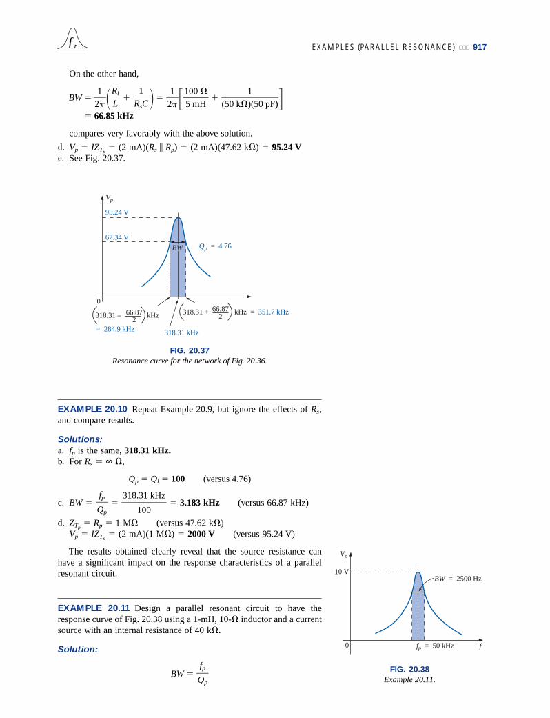
On the other hand,
BW 66.85 kHz
compares very favorably with the above solution.
d. Vp IZTp (2 mA)(Rs Rp) (2 mA)(47.62 k) 95.24 V
e. See Fig. 20.37.
1(50 k)(50 pF)
100 5 mH
12p
1RsC
RlL
12p
ƒr
EXAMPLE 20.10 Repeat Example 20.9, but ignore the effects of Rs,and compare results.
Solutions:
a. fp is the same, 318.31 kHz.b. For Rs ∞ ,
Qp Ql 100 (versus 4.76)
c. BW 3.183 kHz (versus 66.87 kHz)
d. ZTp Rp 1 M (versus 47.62 k)
Vp IZTp (2 mA)(1 M) 2000 V (versus 95.24 V)
The results obtained clearly reveal that the source resistance canhave a significant impact on the response characteristics of a parallelresonant circuit.
EXAMPLE 20.11 Design a parallel resonant circuit to have theresponse curve of Fig. 20.38 using a 1-mH, 10- inductor and a currentsource with an internal resistance of 40 k.
Solution:
BW fp
Qp
318.31 kHz
100
fpQp
FIG. 20.37
Resonance curve for the network of Fig. 20.36.
Vp
95.24 V
67.34 V
0
318.31 – kHz66.872
318.31 + kHz = 351.7 kHz66.872
318.31 kHz= 284.9 kHz
Qp = 4.76BW
BW = 2500 Hz
fp = 50 kHz f0
Vp
10 V
FIG. 20.38
Example 20.11.

918 RESONANCE
Therefore,
Qp 20
XL 2pfpL 2p(50 kHz)(1 mH) 314
and Ql 31.4
Rp Q2lR (31.4)2(10 ) 9859.6
Qp 20 (from above)
so that 6280
resulting in Rs 17.298 k
However, the source resistance was given as 40 k. We must there-fore add a parallel resistor (R′) that will reduce the 40 k to approxi-mately 17.298 k; that is,
17.298 k
Solving for R′:
R′ 30.481 k
The closest commercial value is 30 k. At resonance, XL XC, and
XC
C
and C 0.01 mF (commercially available)
ZTp Rs Q2
lRl
17.298 k 9859.6 6.28 k
with Vp IZTp
and I 1.6 mA
The network appears in Fig. 20.39.
10 V6.28 k
VpZTp
12p(50 kHz)(314 )
12pfp XC
12pfpC
(40 k)(R′)40 k R′
(Rs)(9859.6)Rs 9859.6
Rs 9859.6
314
RXL
314 10
XLRl
50,000 Hz2500 Hz
fpBW
ƒr
Rs 40 k R 30 k
Rl 10
I 1.6 mA
L 1 mH
C 0.01 mF
FIG. 20.39
Network designed to meet the criteria of Fig. 20.38.

APPLICATIONS 919
20.13 APPLICATIONS
Stray Resonance
Stray resonance, like stray capacitance and inductance and unexpectedresistance levels, can occur in totally unexpected situations and canseverely affect the operation of a system. All that is required to producestray resonance would be, for example, a level of capacitance intro-duced by parallel wires or copper leads on a printed circuit board, orsimply two parallel conductive surfaces with residual charge and induc-tance levels associated with any conductor or components such as taperecorder heads, transformers, and so on, that provide the elements nec-essary for a resonance effect. In fact, this resonance effect is a verycommon effect in the everyday cassette tape recorder. The play/recordhead is a coil that can act like an inductor and an antenna. Combine thisfactor with the stray capacitance and real capacitance in the network toform the tuning network, and the tape recorder with the addition of asemiconductor diode can respond like an AM radio. As you plot the fre-quency response of any transformer, you will normally find a regionwhere the response has a peaking effect (look ahead at Fig. 25.23). Thispeaking is due solely to the inductance of the coils of the transformerand the stray capacitance between the wires.
In general, any time you see an unexpected peaking in the frequencyresponse of an element or a system, it is normally caused by a reso-nance condition. If the response has a detrimental effect on the overalloperation of the system, a redesign may be in order, or a filter can beadded that will block the frequencies that result in the resonance condi-tion. Of course, when you add a filter composed of inductors and/orcapacitors, you must be careful that you don’t add another unexpectedresonance condition. It is a problem that can be properly weighed onlyby constructing the system and exposing it to the full range of tests.
Graphic and Parametric Equalizers
We have all noticed at one time or another that the music we hear in aconcert hall doesn’t quite sound the same when we play it at home onour entertainment center. Even after we check the specifications of thespeakers and amplifiers and find that both are nearly perfect (and themost expensive we can afford), the sound is still not what it should be.In general, we are experiencing the effects of the local environmentalcharacteristics on the sound waves. Some typical problems are hardwalls or floors (stone, cement) that will make high frequencies soundlouder. Curtains and rugs, on the other hand, will absorb high frequen-cies. The shape of the room and the placement of the speakers and fur-niture will also affect the sound that reaches our ears. Another criterionis the echo or reflection of sound that will occur in the room. Concerthalls are designed very carefully with their vaulted ceilings and curvedwalls to allow a certain amount of echo. Even the temperature andhumidity characteristics of the surrounding air will affect the quality ofthe sound. It is certainly impossible, in most cases, to redesign your lis-tening area to match a concert hall, but with the proper use of electronicsystems you can develop a response that will have all the qualities thatyou can expect from a home entertainment center.
For a quality system a number of steps can be taken: characteriza-tion and digital delay (surround sound) and proper speaker and ampli-
ƒr

920 RESONANCE ƒr
FIG. 20.40
(a) Dual-channel 15-band “Constant Q” graphic equalizer (Courtesy of ARXSystems.); (b) setup; (c) frequency response.
Full-rangespeaker
Full-rangespeaker
Amplifier and speaker(woofer or subwoofer)
Pink noisethroughout
≅ 10′
MicrophoneGraphicand/orparametricequalizers
(Mid-range,low-power)
(Full-range,low-power)
(Full-range,low-power)
“Surround sound”speakers
(b)
10 Hz 100 Hz 1 kHz 10 kHz 100 kHz f(log scale)31 Hz 63 Hz 125 Hz 250 Hz 500 Hz 2 kHz 4 kHz 8 kHz 16 kHz
Volume
(c)
(a)
APPLICATIONS 921
fier selection and placement. Characterization is a process whereby athorough sound absorption check of the room is performed and the fre-quency response determined. A graphic equalizer such as appearing inFig. 20.40(a) is then used to make the response “flat” for the full rangeof frequencies. In other words, the room is made to appear as though allthe frequencies receive equal amplification in the listening area. Forinstance, if the room is fully carpeted with full draping curtains, therewill be a lot of high-frequency absorption, requiring that the high fre-quencies have additional amplification to match the sound levels of themid and low frequencies. To characterize the typical rectangular-shapedroom, a setup such as shown in Fig. 20.40(b) may be used. The ampli-fier and speakers are placed in the center of one wall, with additionalspeakers in the corners of the room facing the reception area. A mike isthen placed in the reception area about 10 ft from the amplifier and cen-tered between the two other speakers. A pink noise will then be sent outfrom a spectrum analyzer (often an integral part of the graphic equal-izer) to the amplifier and speakers. Pink noise is actually a square-wavesignal whose amplitude and frequency can be controlled. A square-wave signal was chosen because a Fourier breakdown of a square-wavesignal will result in a broad range of frequencies for the system tocheck. You will find in Chapter 24 that a square wave can be con-structed of an infinite series of sine waves of different frequencies.Once the proper volume of pink noise is established, the spectrum ana-lyzer can be used to set the response of each slide band to establish thedesired flat response. The center frequencies for the slides of thegraphic equalizer of Fig. 20.40(a) are provided in Fig. 20.40(c), alongwith the frequency response for a number of adjoining frequenciesevenly spaced on a logarithmic scale. Note that each center frequencyis actually the resonant frequency for that slide. The design is such thateach slide can control the volume associated with that frequency, butthe bandwidth and frequency response stay fairly constant. A goodspectrum analyzer will have each slide set against a decibel (dB) scale(decibels will be discussed in detail in Chapter 23). The decibel scalesimply establishes a scale for the comparison of audio levels. At a nor-mal listening level, usually a change of about 3 dB is necessary for theaudio change to be detectable by the human ear. At low levels of sound,a 2-dB change may be detectable, but at loud sounds probably a 4-dBchange would be necessary for the change to be noticed. These are notstrict laws but simply rules of thumb commonly used by audio techni-cians. For the room in question, the mix of settings may be as shown inFig. 20.40(c). Once set, the slides are not touched again. A flat responsehas been established for the room for the full audio range so that everysound or type of music is covered.
A parametric equalizer such as appearing in Fig. 20.41 is similar toa graphic equalizer, but instead of separate controls for the individualfrequency ranges, it uses three basic controls over three or four broaderfrequency ranges. The typical controls—the gain, center frequency, and
ƒr
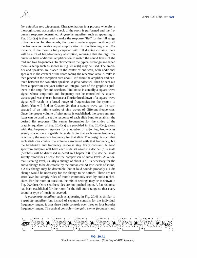
FIG. 20.41
Six-channel parametric equalizer. (Courtesy of ARX Systems.)

922 RESONANCE
bandwidth—are typically available for the low-, mid-, and high-frequency ranges. Each is fundamentally an independent control; that is,a change in one can be made without affecting the other two. For theparametric equalizer of Fig. 20.41, each of the six channels has a fre-quency control switch which, in conjunction with the f 10 switch, willgive a range of center frequencies from 40 Hz through 16 kHz. It hascontrols for BW (“Q”) from 3 octaves to 1⁄20 octave, and 18 dB cut andboost. Some like to refer to the parametric equalizer as a sophisticatedtone control and will actually use them to enrich the sound after the flatresponse has been established by the graphic equalizer. The effectachieved with a standard tone control knob is sometimes referred to as“boring” compared to the effect established by a good parametric equal-izer, primarily because the former can control only the volume and notthe bandwidth or center frequency. In general, graphic equalizers estab-lish the important flat response while parametric equalizers are adjustedto provide the type and quality of sound you like to hear. You can“notch out” the frequencies that bother you and remove tape “hiss” andthe “sharpness” often associated with CDs.
One characteristic of concert halls that is more difficult to fake is thefullness of sound that concert halls are able to provide. In the concerthall you have the direct sound from the instruments and the reflectionof sound off the walls and the vaulted ceilings which were all carefullydesigned expressly for this purpose. Any reflection results in a delay inthe sound waves reaching the ear, creating the fullness effect. Throughdigital delay, speakers can be placed to the back and side of a listenerto establish the surround sound effect. In general, the delay speakers aremuch lower in wattage, with 20-W speakers typically used with a 100-Wsystem. The echo response is one reason that people often like to playtheir stereos louder than they should for normal hearing. By playing thestereo louder, they create more echo and reflection off the walls, bring-ing into play some of the fullness heard at concert halls.
It is probably safe to say that any system composed of quality com-ponents, a graphic and parametric equalizer, and surround sound willhave all the components necessary to have a quality reproduction of theconcert hall effect.
20.14 COMPUTER ANALYSIS
PSpice
Series Resonance This chapter provides an excellent opportunityto demonstrate what computer software programs can do for us. Imag-ine having to plot a detailed resonance curve with all the calculationsrequired for each frequency. At every frequency, the reactance of theinductive and capacitive elements changes, and the phasor operationswould have to be repeated—a long and arduous task. However, withPSpice, taking a few moments to enter the circuit and establish thedesired simulation will result in a detailed plot in a few seconds that canhave plot points every microsecond!
For the first time, the horizontal axis will be in the frequency domainrather than in the time domain as in all the previous plots. For the seriesresonant circuit of Fig. 20.42, the magnitude of the source was chosento produce a maximum current of I 400 mV/40 10 mA at reso-nance, and the reactive elements will establish a resonant frequency of
ƒr

COMPUTER ANALYSIS 923
fs 2.91 kHz
The quality factor is
Ql X
RL
l
54
4
6
0
.6
4 13.7
which is relatively high and should give us a nice sharp response.The bandwidth is
BW Q
fs
l
2.9
1
1
3.
k
7
Hz 212 Hz
which will be verified using our cursor options.For the ac source, VSIN was chosen again. All the parameters were
set by double-clicking on the source symbol and entering the values inthe Property Editor dialog box. For each, Name and Value wasselected under Display followed by Apply before leaving the dialogbox.
In the Simulation Settings dialog box, AC Sweep/Noise wasselected, and the Start Frequency was set at 1 kHz, the End Fre-quency at 10 kHz, and the Points/Decade at 10,000. The Logarithmicscale and Decade settings remain at their default values. The 10,000 forPoints/Decade was chosen to ensure a number of data points near thepeak value. When the SCHEMATIC1 screen of Fig. 20.43 appears,Trace-Add Trace-I(R)-OK will result in a logarithmic plot that peaksjust to the left of 3 kHz. The spacing between grid lines on the X-axisshould be increased, so Plot-Axis Settings-X Grid-unable Automatic-Spacing-Log-0.1-OK is implemented. Next, select the Toggle cursor
12p(30 mH)(0.1mF)
12pLC
ƒr
FIG. 20.42
Series resonant circuit to be analyzed using PSpice.

924 RESONANCE
icon, and with a right click of the mouse move the right cursor as closeto 7.07 mA as possible (0.707 of the peak value to define the band-width) to obtain A1 with a frequency of 3.02 kHz at a level of 7.01 mA—the best we can do with the 10,000 data points per decade. Now do aleft click, and place the left cursor as close to the same level as possi-ble. The result is 2.8 kHz at a level of 7.07 mA for A2. The cursorswere set in the order above to obtain a positive answer for the differenceof the two as appearing in the third line of the Probe Cursor box. Theresulting 214.22 Hz is an excellent match with the calculated value of212 Hz.
Parallel Resonance Let us now investigate the parallel resonant cir-cuit of Fig. 20.33 and compare the results with the longhand solution.The network appears in Fig. 20.44 using ISRC as the ac source voltage.Under the Property Editor heading, the following values were set:DC 0 A, AC 2 mA, and TRAN 0. Under Display, Do NotDisplay was selected for both DC and TRAN since they do not play apart in our analysis. In the Simulation Settings dialog box, AC Sweep/Noise was selected, and the Start Frequency was selected as 10 kHzsince we know that it will resonate near 30 kHz. The End Frequencywas chosen as 100 kHz for a first run to see the results. The Points/Decade was set at 10,000 to ensure a good number of data points forthe peaking region. After simulation, Trace-Add Trace-V(C:1)-OKresulted in the plot of Fig. 20.45 with a resonant frequency near 30 kHz.The selected range appears to be a good one, but the initial plot neededmore grid lines on the x-axis, so Plot-Axis Settings-X-Grid-unenableAutomatic-Spacing-Log-0.1-OK was used to obtain a grid line at 10-kHzintervals. Next the Toggle cursor pad was selected and a left-click
ƒr
FIG. 20.43
Resonance curve for the current of the circuit of Fig. 20.42.
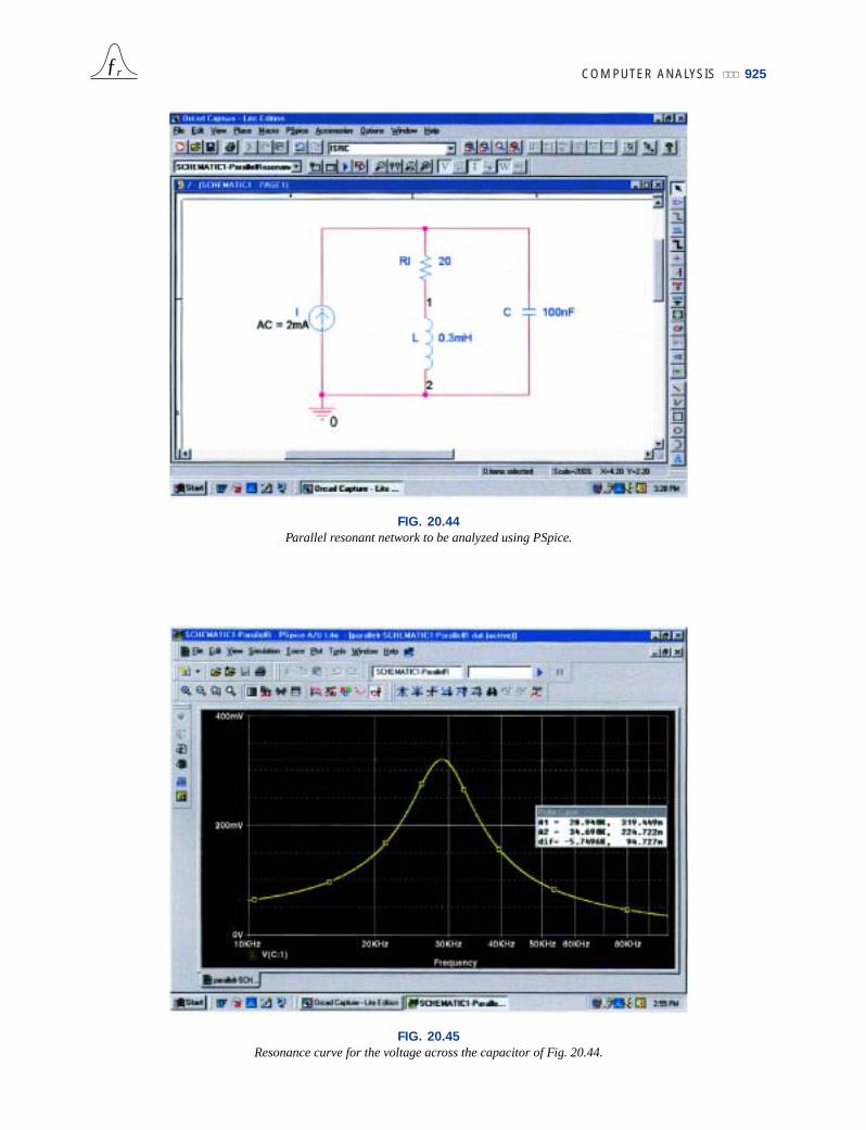
COMPUTER ANALYSIS 925ƒr
FIG. 20.44
Parallel resonant network to be analyzed using PSpice.
FIG. 20.45
Resonance curve for the voltage across the capacitor of Fig. 20.44.

926 RESONANCE
cursor established on the screen. The Cursor Peak pad was then cho-sen to find the peak value of the curve. The result was A1 319.45 mVat 28.94 kHz which is a very close match with the calculated value of318.68 mV at 28.57 kHz for the maximum value of VC. The bandwidthis defined at a level of 0.707(319.45 mV) 225.85 mV. Using theright-click cursor, we find that the closest we can come is 224.72 mVfor the 10,000 points of data per decade. The resulting frequency is34.69 kHz as shown in the Probe Cursor box of Fig. 20.45.
We can now use the left-click cursor to find the same level to the leftof the peak value so that we can determine the bandwidth. The closestthat the left-click cursor can come to 225.85 mV is 224.96 mV at a fre-quency of 23.97 kHz. The bandwidth will then appear as 10.72 kHz inthe Probe Cursor box, comparing very well with the longhand solutionof 10.68 kHz in Example 20.7.
It would now be interesting to look at the phase angle of the voltageacross the parallel network to find the frequency when the networkappears resistive and the phase angle is 0°. First use Trace-Delete AllTraces, and call up P(V(C:1)) followed by OK. The result is the plotof Fig. 20.46, revealing that the phase angle is close to 90° at veryhigh frequencies as the capacitive element with its decreasing reactancetakes over the characteristics of the parallel network. At 10 kHz theinductive element has a lower reactance than the capacitive element,and the network has a positive phase angle. Using the cursor option, wecan move the left click along the horizontal axis until the phase angle isat its minimum value. As shown in Fig. 20.46, the smallest angle avail-able with the determined data points is 49.86 mdegrees 0.05° whichis certainly very close to 0°. The corresponding frequency is 27.046 kHzwhich is essentially an exact match with the longhand solution of
ƒr
FIG. 20.46
Phase plot for the voltage vC for the parallel resonant network of Fig. 20.44.

COMPUTER ANALYSIS 927
27.051 kHz. Clearly, therefore, the frequency at which the phase angleis zero and the total impedance appears resistive is less than the fre-quency at which the output voltage is a maximum.
Electronics Workbench
The results of Example 20.9 will now be confirmed using ElectronicsWorkbench. The network of Fig. 20.36 will appear as shown in Fig.20.47 after all the elements have been placed as described in earlierchapters. In particular, note that the frequency assigned to the 2-mA accurrent source is 100 kHz. Since we have some idea that the resonantfrequency is a few hundred kilohertz, it seemed appropriate that thestarting frequency for the plot begin at 100 kHz and extend to 1 MHz.Also, be sure that the AC Magnitude is set to 2 mA in the AnalysisSetup within the AC Current dialog box.
ƒr
FIG. 20.47
Using Electronics Workbench to confirm the results of Example 20.9.
For simulation, the sequence Simulate-Analyses-AC Analysis isfirst selected to obtain the AC Analysis dialog box. The Start fre-quency is set at 100 kHz, and the Stop frequency at 1 MHz; Sweeptype is Decade; Number of points per decade is 1000; and the Verti-cal scale is Linear. Under Output variables, node number 1 is selectedas a Variable for analysis followed by Simulate to run the program.The results are the magnitude and phase plots of Fig. 20.48. Startingwith the Voltage plot, the Show/Hide Grid key, Show/Hide Legendkey, and Show/Hide Cursors key are selected. You will immediatelynote under the AC Analysis cursor box that the maximum value is95.24 V and the minimum value is 6.94 V. By moving the cursor untilwe reach 95.24 V (y1), the resonant frequency can be found. As shown
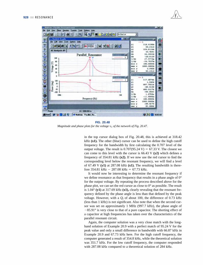
928 RESONANCE
in the top cursor dialog box of Fig. 20.48, this is achieved at 318.42kHz (x1). The other (blue) cursor can be used to define the high cutofffrequency for the bandwidth by first calculating the 0.707 level of theoutput voltage. The result is 0.707(95.24 V) 67.33 V. The closest wecan come to this level with the cursor is 66.43 V (y2) which defines afrequency of 354.81 kHz (x2). If we now use the red cursor to find thecorresponding level below the resonant frequency, we will find a levelof 67.49 V (y1) at 287.08 kHz (x1). The resulting bandwidth is there-fore 354.81 kHz 287.08 kHz 67.73 kHz.
It would now be interesting to determine the resonant frequency ifwe define resonance as that frequency that results in a phase angle of 0°for the output voltage. By repeating the process described above for thephase plot, we can set the red cursor as close to 0° as possible. The resultis 1.04° (y1) at 317.69 kHz (x1), clearly revealing that the resonant fre-quency defined by the phase angle is less than that defined by the peakvoltage. However, with a Ql of about 100, the difference of 0.73 kHz(less than 1 kHz) is not significant. Also note that when the second cur-sor was set on approximately 1 MHz (997.7 kHz), the phase angle of85.91° is very close to that of a pure capacitor. The shorting effect ofa capacitor at high frequencies has taken over the characteristics of theparallel resonant circuit.
Again, the computer solution was a very close match with the long-hand solution of Example 20.9 with a perfect match of 95.24 V for thepeak value and only a small difference in bandwidth with 66.87 kHz inExample 20.9 and 67.73 kHz here. For the high cutoff frequency, thecomputer generated a result of 354.8 kHz, while the theoretical solutionwas 351.7 kHz. For the low cutoff frequency, the computer respondedwith 287.08 kHz compared to a theoretical solution of 284 kHz.
ƒr
FIG. 20.48
Magnitude and phase plots for the voltage vC of the network of Fig. 20.47.

PROBLEMS 929ƒr
PROBLEMS
SECTIONS 20.2 THROUGH 20.7 Series Resonance
1. Find the resonant qs and fs for the series circuit with thefollowing parameters:a. R 10 , L 1 H, C 16 mFb. R 300 , L 0.5 H, C 0.16 mFc. R 20 , L 0.28 mH, C 7.46 mF
2. For the series circuit of Fig. 20.49:a. Find the value of XC for resonance.b. Determine the total impedance of the circuit at reso-
nance.c. Find the magnitude of the current I.d. Calculate the voltages VR, VL, and VC at resonance.
How are VL and VC related? How does VR compare tothe applied voltage E?
e. What is the quality factor of the circuit? Is it a high-or low-Q circuit?
f. What is the power dissipated by the circuit at reso-nance?
3. For the series circuit of Fig. 20.50:a. Find the value of XL for resonance.b. Determine the magnitude of the current I at reso-
nance.c. Find the voltages VR, VL, and VC at resonance, and
compare their magnitudes.d. Determine the quality factor of the circuit. Is it a high-
or low-Q circuit?e. If the resonant frequency is 5 kHz, determine the value
of L and C.f. Find the bandwidth of the response if the resonant fre-
quency is 5 kHz.g. What are the low and high cutoff frequencies?
4. For the circuit of Fig. 20.51:a. Find the value of L in millihenries if the resonant fre-
quency is 1800 Hz.b. Calculate XL and XC. How do they compare?c. Find the magnitude of the current Irms at resonance.d. Find the power dissipated by the circuit at resonance.e. What is the apparent power delivered to the system at
resonance?f. What is the power factor of the circuit at resonance?g. Calculate the Q of the circuit and the resulting band-
width.h. Find the cutoff frequencies, and calculate the power
dissipated by the circuit at these frequencies.
5. a. Find the bandwidth of a series resonant circuit havinga resonant frequency of 6000 Hz and a Qs of 15.
b. Find the cutoff frequencies.c. If the resistance of the circuit at resonance is 3 ,
what are the values of XL and XC in ohms?d. What is the power dissipated at the half-power fre-
quencies if the maximum current flowing through thecircuit is 0.5 A?
6. A series circuit has a resonant frequency of 10 kHz. Theresistance of the circuit is 5 , and XC at resonance is200 .a. Find the bandwidth.
VR
R = 10 +
–
E 50 mV
VL+ –
+
–XC VC
I XL = 30
+ –
FIG. 20.49
Problem 2.
XC
VR
R = 2 XLI
+ – VL+ –
VC
+
–
+
–
E 20 mV 40
FIG. 20.50
Problem 3.
C
R
4.7 I
L
+
–
e 2 mF20 10–3 sin qt
FIG. 20.51
Problem 4.

b. Find the cutoff frequencies.c. Find Qs.d. If the input voltage is 30 V 0°, find the voltage across
the coil and capacitor in phasor form.e. Find the power dissipated at resonance.
7. a. The bandwidth of a series resonant circuit is 200 Hz.If the resonant frequency is 2000 Hz, what is thevalue of Qs for the circuit?
b. If R 2 , what is the value of XL at resonance?c. Find the value of L and C at resonance.d. Find the cutoff frequencies.
8. The cutoff frequencies of a series resonant circuit are 5400 Hz and 6000 Hz.a. Find the bandwidth of the circuit.b. If Qs is 9.5, find the resonant frequency of the circuit.c. If the resistance of the circuit is 2 , find the value of
XL and XC at resonance.d. Find the value of L and C at resonance.
*9. Design a series resonant circuit with an input voltage of 5 V 0° to have the following specifications:a. A peak current of 500 mA at resonanceb. A bandwidth of 120 Hzc. A resonant frequency of 8400 HzFind the value of L and C and the cutoff frequencies.
*10. Design a series resonant circuit to have a bandwidth of400 Hz using a coil with a Ql of 20 and a resistance of 2 . Find the values of L and C and the cutoff frequen-cies.
*11. A series resonant circuit is to resonate at qs 2p 106 rad/s and draw 20 W from a 120-V source atresonance. If the fractional bandwidth is 0.16:a. Determine the resonant frequency in hertz.b. Calculate the bandwidth in hertz.c. Determine the values of R, L, and C.d. Find the resistance of the coil if Ql 80.
*12. A series resonant circuit will resonate at a frequency of 1 MHz with a fractional bandwidth of 0.2. If the qualityfactor of the coil at resonance is 12.5 and its inductanceis 100 mH, determine the following:a. The resistance of the coil.b. The additional resistance required to establish the indi-
cated fractional bandwidth.c. The required value of capacitance.
930 RESONANCE ƒr
LRs 2 k 0.1 mH C = 10 nF VC
+
–
ICIL
I 2 mA
FIG. 20.52
Problem 13.
SECTIONS 20.8 THROUGH 20.12
Parallel Resonance
13. For the “ideal” parallel resonant circuit of Fig. 20.52:a. Determine the resonant frequency ( fp).b. Find the voltage VC at resonance.c. Determine the currents IL and IC at resonance.d. Find Qp.

PROBLEMS 931ƒr
14. For the parallel resonant network of Fig. 20.53:a. Calculate fs.b. Determine Ql using f fs. Can the approximate
approach be applied?c. Determine fp and fm.d. Calculate XL and XC using fp. How do they compare?e. Find the total impedance at resonance ( fp).f. Calculate VC at resonance ( fp).g. Determine Qp and the BW using fp.h. Calculate IL and IC at fp.
FIG. 20.54
Problem 15.
FIG. 20.55
Problem 16.
FIG. 20.53
Problem 14.
16. For the network of Fig. 20.55:a. Find the value of XC at resonance ( fp).b. Find the total impedance ZTp
at resonance ( fp).c. Find the currents IL and IC at resonance ( fp).d. If the resonant frequency is 20,000 Hz, find the value
of L and C at resonance.e. Find Qp and the BW.
FIG. 20.56
Problem 17.
L 0.1 mH
2 F VC
+
–I 2 mA
Rs = ∞
C
Rl 4
ZTp
Rl
XC
IC20
XL 100
ILZTp
Rs 1 k
I = 5 mA ∠ 0°
Rl
XC
IC2
XL 30
ILZTp
Rs 450
I = 80 mA ∠ 0°
L 0.5 mH
30 nF VC
+
–I 10 mA
Rs = ∞
C
Rl 8
ZTp
15. Repeat Problem 14 for the network of Fig. 20.54.
17. Repeat Problem 16 for the network of Fig. 20.56.

932 RESONANCE ƒr
18. For the network of Fig. 20.57:a. Find the resonant frequencies fs, fp, and fm. What do
the results suggest about the Qp of the network?b. Find the values of XL and XC at resonance ( fp). How
do they compare?c. Find the impedance ZTp
at resonance ( fp).d. Calculate Qp and the BW.e. Find the magnitude of currents IL and IC at resonance
( fp).f. Calculate the voltage VC at resonance ( fp).
*19. Repeat Problem 18 for the network of Fig. 20.58.
20. It is desired that the impedance ZT of the high-Q circuitof Fig. 20.59 be 50 k 0° at resonance ( fp).a. Find the value of XL.b. Compute XC.c. Find the resonant frequency ( fp) if L 16 mH.d. Find the value of C.
FIG. 20.57
Problem 18.
21. For the network of Fig. 20.60:a. Find fp.b. Calculate the magnitude of VC at resonance ( fp).c. Determine the power absorbed at resonance.d. Find the BW.
Rl
C
IC1.5
L 80 mH
IL
ZTp
Rs 10 kI 10 mA 0.03 mF VC
+
–
FIG. 20.58
Problems 19 and 29.
Rl
C
IC8
L 0.5 mH
IL
ZTp
Rs 0.5 kI 40 mA 1 mF VC
+
–
FIG. 20.59
Problem 20.
FIG. 20.60
Problem 21.
XL
Rl 50
XCZT
L
Rl
40 k C0.01 mF
VC
+
–
Ql = 20
200 mH
Rs
I = 5 mA ∠ 0°

PROBLEMS 933ƒr
*22. For the network of Fig. 20.61:a. Find the value of XL for resonance.b. Find Ql.c. Find the resonant frequency ( fp) if the bandwidth is
1 kHz.d. Find the maximum value of the voltage VC.e. Sketch the curve of VC versus frequency. Indicate its
peak value, resonant frequency, and band frequencies.FIG. 20.61
Problem 22.
FIG. 20.62
Problem 23.
FIG. 20.63
Problem 24.
*23. Repeat Problem 22 for the network of Fig. 20.62.
*24. For the network of Fig. 20.63:a. Find fs, fp, and fm.b. Determine Ql and Qp at fp after a source conversion is
performed.c. Find the input impedance ZTp.
d. Find the magnitude of the voltage VC.e. Calculate the bandwidth using fp.f. Determine the magnitude of the currents IC and IL.
*25. For the network of Fig. 20.64, the following are speci-fied:
fp 20 kHzBW 1.8 kHz
L 2 mHQl 80
Find Rs and C.
XL
Rl
20 k XC 400 VC
+
–
RsI = 0.1 mA
8
XL
Rl
40 k XC 100 VC
+
–
RsI = 6 mA ∠ 0°
12
FIG. 20.64
Problem 25.
Rl 6
Rs
20 kIL
IC
C1 20 nF
C2 10 nFVC
+
–L 0.5 mH
E = 80 V ∠ 0°
+
–ZTp
C
Rl
Ql
L
Rs
0.2 mA 0° C
L
Rl
I
Rs = ∞ Ω
FIG. 20.65
Problem 26.
*26. Design the network of Fig. 20.65 to have the followingcharacteristics:a. BW 500 Hzb. Qp 30c. VCmax
1.8 V

Resonance A condition established by the application of aparticular frequency (the resonant frequency) to a series orparallel R-L-C network. The transfer of power to the systemis a maximum, and, for frequencies above and below, thepower transfer drops off to significantly lower levels.
Selectivity A characteristic of resonant networks directlyrelated to the bandwidth of the resonant system. High selec-tivity is associated with small bandwidth (high Q’s), andlow selectivity with larger bandwidths (low Q’s).
934 RESONANCE ƒr
GLOSSARY
Band (cutoff, half-power, corner) frequencies Frequenciesthat define the points on the resonance curve that are 0.707of the peak current or voltage value. In addition, they definethe frequencies at which the power transfer to the resonantcircuit will be half the maximum power level.
Bandwidth (BW) The range of frequencies between theband, cutoff, or half-power frequencies.
Quality factor (Q) A ratio that provides an immediate indi-cation of the sharpness of the peak of a resonance curve.The higher the Q, the sharper the peak and the more quicklyit drops off to the right and left of the resonant frequency.
*27. For the parallel resonant circuit of Fig. 20.66:a. Determine the resonant frequency.b. Find the total impedance at resonance.c. Find Qp.d. Calculate the BW.e. Repeat parts (a) through (d) for L 20 mH and C
20 nF.f. Repeat parts (a) through (d) for L 0.4 mH and C
1 nF.g. For the network of Fig. 20.66 and the parameters of
parts (e) and (f), determine the ratio L/C.h. Do your results confirm the conclusions of Fig. 20.28
for changes in the L /C ratio?
SECTION 20.14 Computer Analysis
PSpice or Electronics Workbench
28. Verify the results of Example 20.8. That is, show that theresonant frequency is in fact 40 kHz, the cutoff frequen-cies are as calculated, and the bandwidth is 1.85 kHz.
29. Find fp and fm for the parallel resonant network of Fig.20.58, and comment on the resulting bandwidth as itrelates to the quality factor of the network.
Programming Language (C, QBASIC, Pascal, etc.)
30. Write a program to tabulate the impedance and current ofthe network of Fig. 20.2 versus frequency for a frequencyrange extending from 0.1fs to 2 fs in increments of 0.1fs.For the first run, use the parameters defined by Example20.1.
31. Write a program to provide a general solution for the net-work of Fig. 20.36; that is, determine the parametersrequested in parts (a) through (e) of Example 20.9.
FIG. 20.66
Problem 27.
Rl 20
40 k
L 200 H
C 2 nFZTp