2025-7 satellite navigation science and technology for...
TRANSCRIPT

2025-7
Satellite Navigation Science and Technology for Africa
Ward Phillip. W.
23 March - 9 April, 2009
NavwardU.S.A
Introduction to GPS Receiver Design Principles(Part 4)

Session IVCarrier tracking loop design
Generic GPS receiver carrier tracking loop block diagramPhase lock loopsI,Q diagram depicting true PLL phase errorFrequency lock loopsI,Q diagram depicting true frequency error
Generic GPS receiver carrier tracking loop block diagram
Carrier tracking loop description spread out over several block diagrams
Carrier synthesis hardwareCarrier then code wipe-off hardwarePredetection integration hardwareBaseband software
Carrier loop discriminator and filterDiscriminator defines carrier loop type
Phase or frequency lock loop (PLL or FLL)
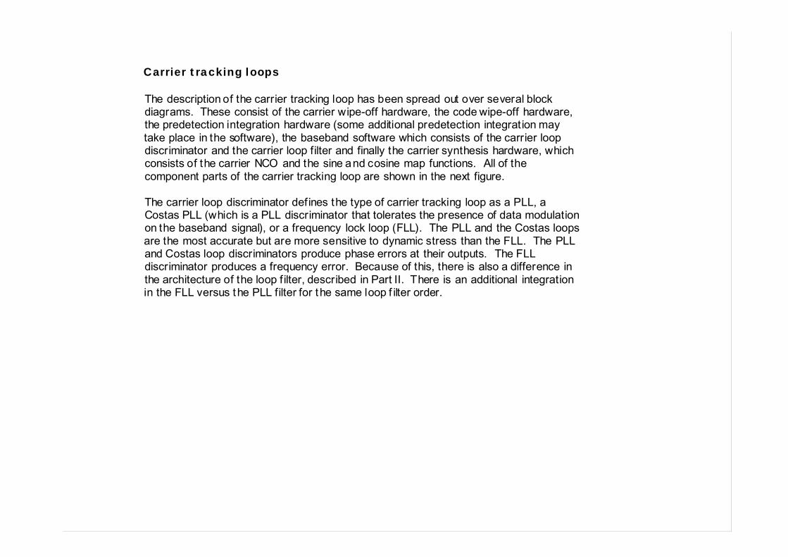
Carrier tracking loops
The description of the carrier tracking loop has been spread out over several blockdiagrams. These consist of the carrier wipe-off hardware, the code wipe-off hardware,the predetection integration hardware (some additional predetection integration maytake place in the software), the baseband software which consists of the carrier loopdiscriminator and the carrier loop filter and finally the carrier synthesis hardware, whichconsists of the carrier NCO and the sine and cosine map functions. All of thecomponent parts of the carrier tracking loop are shown in the next figure.
The carrier loop discriminator defines the type of carrier tracking loop as a PLL, aCostas PLL (which is a PLL discriminator that tolerates the presence of data modulationon the baseband signal), or a frequency lock loop (FLL). The PLL and the Costas loopsare the most accurate but are more sensitive to dynamic stress than the FLL. The PLLand Costas loop discriminators produce phase errors at their outputs. The FLLdiscriminator produces a frequency error. Because of this, there is also a difference inthe architecture of the loop filter, described in Part II. There is an additional integrationin the FLL versus the PLL filter for the same loop f ilter order.
Generic GPS receiver carrier tracking loop block diagram
Integrate & dump
Integrate & dump
Carrier loop discriminator
Carrier loop filter
Numerical controlled oscillator
COS map
SIN map
Prompt replica code
SIN replica carrier
COS replica carrier
QPS
IPSI
Q
Carrier wipeoff
Code wipeoff Scale
factor
External velocity aiding
Carrier NCO bias
Carrier aiding to code loopDigital
IF
.
Clock fc
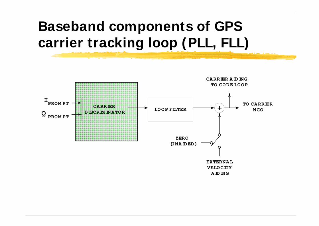
Baseband components of GPS carrier tracking loop (PLL, FLL)
CARRIER AIDING TO CODE LOOP
EXTERNAL VELOCITY AIDING
ZERO (UNAIDED)
TO CARRIER NCOQ PROM PT
IPROM PT+LOOP FILTERCARRIER
DISCRIM INATOR
Designing PLL carrier tracking loop discriminators
Phase lock loop (PLL) discriminators Common phase lock loop discriminatorsComparison of PLL discriminatorsI,Q diagram depicting true PLL phase error

Common phase lock loop discriminators
Discriminatoralgorithm
Outputphaseerror
Characteristics(First four are data insensitive.
Last is pure PLL)
Sign (IPS )*QPS sin (φ) Decision directed Costas. Near optimal at high SNR. Slopeproportional to signal amplitude A. Least computationalburden.
IPS*QPS sin (2φ) Costas. Near optimal at low SNR. Slope proportional to sigamplitude squared A2. Moderate computational burden.
QPS /IPS tan (φ) Suboptimal but good at high and low SNR. Slope not signalamplitude dependent. Higher computational burden andmust check for divide by zero error near ± 90 degrees.
ATAN (QPS/IPS) φ Two-quadrant arctangent. Optimal (maximum likelihoodestimator) at high and low SNR. Slope not signalamplitude dependent. Highest computational burden.
ATAN2 (QPS, IPS) φ Four-quadrant arctangent. Optimal (maximum likelihood eestimator) at high and low SNR. Slope not signalamplitude dependent. Highest computational burden.

Comparison of PLL discriminators
The input/output relationships of the four PLL discriminators that are insensitive to datatransitions in the previous table are plotted below. The true input error in degrees isplotted as the abscissa and the discriminator output error is plotted as the ordinate. Note that the output of all these discriminators repeat every 180 degrees (1/.2 cycle). The ATAN 2 four-quadrant pure PLL discriminator input/output characteristic looks likethe two-quadrant ATAN discriminator input/output characteristic, except that it repeatsevery 360 degrees (cycle). Therefore both its input and output range are doubled. Because the input error range is double the ATAN 2 di scriminator, the pure PLLdiscriminator has 6 dB more noise error tolerance.
The ideal input/output relationship is linear. Therefore, only the ATAN discriminator isoptimal. All of the others are simply approximations to minimize the computationalburden. As a result, their discriminator performance is suboptimal. Their advantagesand limitations are summarized in the table below.

Comparison of PLL discriminators

PLL I, Q phasor diagram: Phase error between replica carrier and incoming carrier
I
Q
φ
φ
A
-A
I P S
P S- IQ
-Q
P S
P ST ru e p h a se erro r = φ
P h a se a m b ig u ity d u e to d a ta b it tra n s itio n

I,Q “fuzz ball” of PLL signal with data plus noise
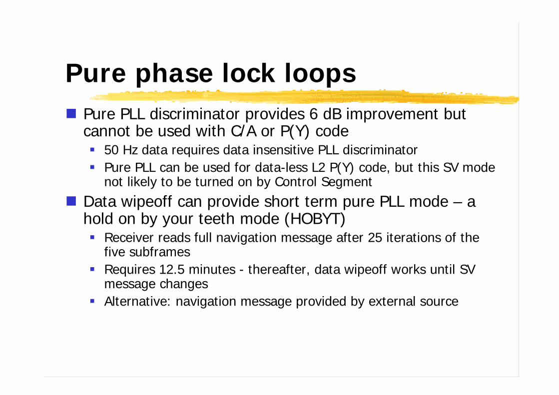
Pure phase lock loopsPure PLL discriminator provides 6 dB improvement but cannot be used with C/A or P(Y) code
50 Hz data requires data insensitive PLL discriminatorPure PLL can be used for data-less L2 P(Y) code, but this SV mode not likely to be turned on by Control Segment
Data wipeoff can provide short term pure PLL mode – a hold on by your teeth mode (HOBYT)
Receiver reads full navigation message after 25 iterations of the five subframesRequires 12.5 minutes - thereafter, data wipeoff works until SV message changesAlternative: navigation message provided by external source

Designing FLL carrier tracking loop discriminators
Frequency lock loop (FLL) discriminators Common FLL discriminatorsComparison of FLL discriminatorsI,Q diagram depicting true frequency error
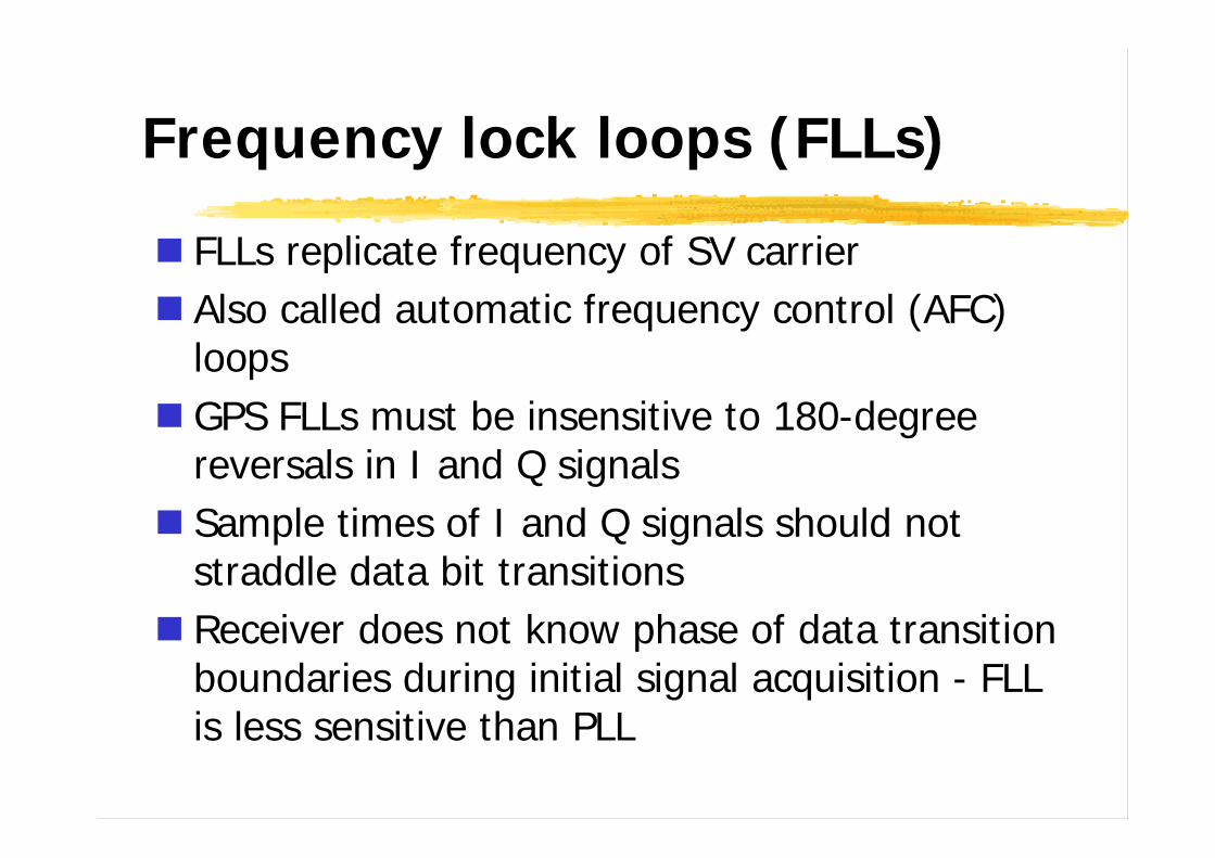
Frequency lock loops (FLLs)
FLLs replicate frequency of SV carrierAlso called automatic frequency control (AFC) loopsGPS FLLs must be insensitive to 180-degree reversals in I and Q signalsSample times of I and Q signals should not straddle data bit transitionsReceiver does not know phase of data transition boundaries during initial signal acquisition - FLL is less sensitive than PLL
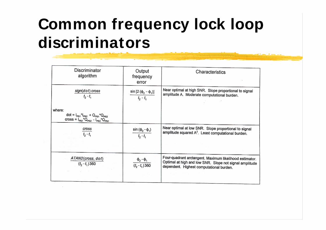
Common frequency lock loop discriminators

Comparison of FLL discriminators

FLL I, Q phasor diagram: frequency error between replica carrier and incoming carrier
Q
I
t 1t 2
φ − φ2 1
QPS1Q PS2
PS1PS2 II
2 A1
-A1 -A2
No frequency ambiguity due to data bit transition (unless samples are split)
φ − φ t − t2 1
2 1True frequency error
-A

Session V